

Page 1
8
+12V_BUS
C1
CAP CER 10UF 20% 16V X5R
10UFC110UF
(1206)1.8MM H MAX
+12V_BUS
+12V_BUS
C2
D D
+3.3V_BUS
+3.3V_BUS
C C
B B
C3
150nF_16VC2150nF_16V
150nF_16VC3150nF_16V
CAP CER 10UF 10% 6.3V X6S
(0805)1.4MM MAX THICK
C5
10uF_X6SC510uF_X6S
C7
1uF_6.3VC71uF_6.3V
C8
10nFC810nF
C6
100nF_6.3VC6100nF_6.3V
Place these caps as close to the PCIE
connector as possible
7
+3.3V
R5
R6
4.7KR54.7K
GPIO_47
GPIO_37
C9
4.7KR64.7K
DNIDNI
100nF_6.3VC9100nF_6.3V
R10RR1
0R
PETp10_GFXRp102
PETn10_GFXRn102
PETp11_GFXRp112
PETn11_GFXRn112
PETp12_GFXRp122
PETn12_GFXRn122
PETp13_GFXRp132
PETn13_GFXRn132
PETp14_GFXRp142
PETn14_GFXRn142
PETp15_GFXRp152
PETn15_GFXRn152
PETn0_GFXRn02
PETp1_GFXRp12
PETn1_GFXRn12
PETp2_GFXRp22
PETn2_GFXRn22
PETp3_GFXRp32
PETn3_GFXRn32
PETp4_GFXRp42
PETn4_GFXRn42
PETp5_GFXRp52
PETn5_GFXRn52
PETp6_GFXRp62
PETn6_GFXRn62
PETp7_GFXRp72
PETn7_GFXRn72
PETp8_GFXRp82
PETn8_GFXRn82
PETp9_GFXRp92
PETn9_GFXRn92
+3.3V_BUS
6
U12
U12
VCC8OE1
1B2OE2
6
1A
2B
4
GND
2A
NC7WB66K8X
NC7WB66K8X
R70R R70R
R80R R80R
DNI , To Bypass U12
+3.3V_BUS
PRESENCE
5
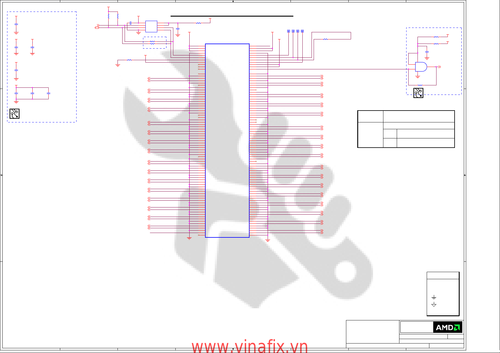
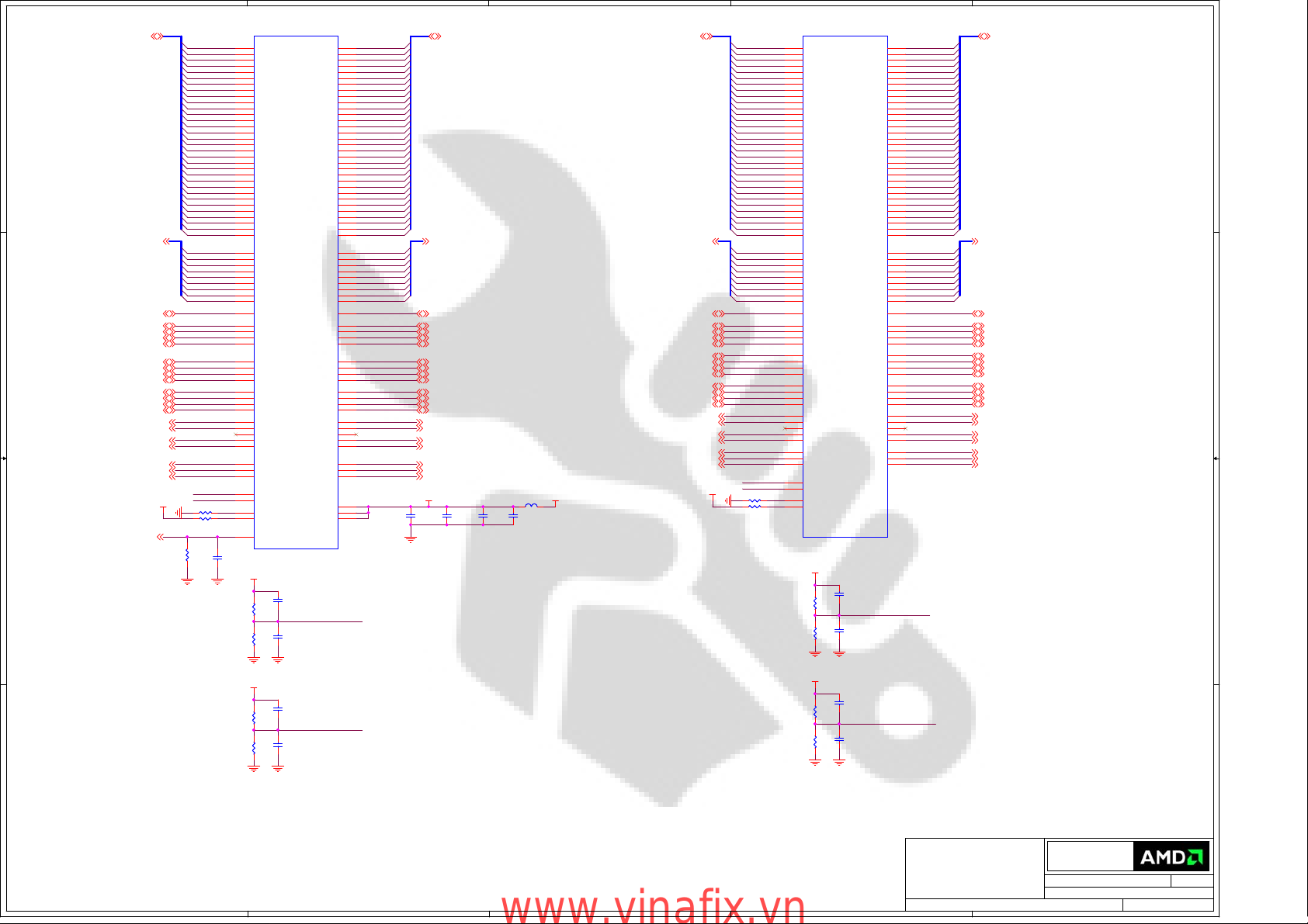
PCI-EXPRESS EDGE CONNECTOR
7
3
1
5
SMCLK
SMDAT
C10
C10
100nF_6.3V
100nF_6.3V
+12V_BUS
+3.3V
R40RR4
0R
x16 PCIe
B1
B2
B3
B4
B5
B6
B7
B8
B9
B10
B11
B12
B13
B14
B15
B16
B17
B18
B19
B20
B21
B22
B23
B24
B25
B26
B27
B28
B29
B30
B31
B32
B33
B34
B35
B36
B37
B38
B39
B40
B41
B42
B43
B44
B45
B46
B47
B48
B49
B50
B51
B52
B53
B54
B55
B56
B57
B58
B59
B60
B61
B62
B63
B64
B65
B66
B67
B68
B69
B70
B71
B72
B73
B74
B75
B76
B77
B78
B79
B80
B81
B82
+12V#B1
+12V#B2
+12V#B3
GND#B4
SMCLK
SMDAT
GND#B7
+3.3V#B8
JTAG1
3.3Vaux
WAKE#
RSVD#B12
GND#B13
PETp0
PETn0
GND#B16
PRSNT2#B17
GND#B18
PETp1
PETn1
GND#B21
GND#B22
PETp2
PETn2
GND#B25
GND#B26
PETp3
PETn3
GND#B29
RSVD#B30
PRSNT2#B31
GND#B32
PETp4
PETn4
GND#B35
GND#B36
PETp5
PETn5
GND#B39
GND#B40
PETp6
PETn6
GND#B43
GND#B44
PETp7
PETn7
GND#B47
PRSNT2#B48
GND#B49
PETp8
PETn8
GND#B52
GND#B53
PETp9
PETn9
GND#B56
GND#B57
PETp10
PETn10
GND#B60
GND#B61
PETp11
PETn11
GND#B64
GND#B65
PETp12
PETn12
GND#B68
GND#B69
PETp13
PETn13
GND#B72
GND#B73
PETp14
PETn14
GND#B76
GND#B77
PETp15
PETn15
GND#B80
PRSNT2#B81
RSVD#B82
x16 PCIe
Mechanical Key
Mechanical Key
MPCIE1
MPCIE1
PRSNT1#A1
+3.3V#A10
RSVD#A19
RSVD#A32
RSVD#A33
RSVD#A50
+12V#A2
+12V#A3
GND#A4
JTAG2
JTAG3
JTAG4
JTAG5
+3.3V#A9
PERST#
GND#A12
REFCLK+
REFCLKGND#A15
PERp0
PERn0
GND#A18
GND#A20
PERp1
PERn1
GND#A23
GND#A24
PERp2
PERn2
GND#A27
GND#A28
PERp3
PERn3
GND#A31
GND#A34
PERp4
PERn4
GND#A37
GND#A38
PERp5
PERn5
GND#A41
GND#A42
PERp6
PERn6
GND#A45
GND#A46
PERp7
PERn7
GND#A49
GND#A51
PERp8
PERn8
GND#A54
GND#A55
PERp9
PERn9
GND#A58
GND#A59
PERp10
PERn10
GND#A62
GND#A63
PERp11
PERn11
GND#A66
GND#A67
PERp12
PERn12
GND#A70
GND#A71
PERp13
PERn13
GND#A74
GND#A75
PERp14
PERn14
GND#A78
GND#A79
PERp15
PERn15
GND#A82
A1
A2
A3
A4
A5
A6
A7
A8
A9
A10
A11
A12
A13
A14
A15
A16
A17
A18
A19
A20
A21
A22
A23
A24
A25
A26
A27
A28
A29
A30
A31
A32
A33
A34
A35
A36
A37
A38
A39
A40
A41
A42
A43
A44
A45
A46
A47
A48
A49
A50
A51
A52
A53
A54
A55
A56
A57
A58
A59
A60
A61
A62
A63
A64
A65
A66
A67
A68
A69
A70
A71
A72
A73
A74
A75
A76
A77
A78
A79
A80
A81
A82
PRESENCE
4
TP1
TP1
TP5
TP5
TP3
TP3
TP2
TP2
35mil
35mil
35mil
35mil
35mil
35mil
35mil
+12V_BUS
JTCK
JTDI
JTDO
JTMS
PERp0
PERn0
PERp1
PERn1
PERp2
PERn2
PERp3
PERn3
PERp4
PERn4
PERp5
PERn5
PERp6
PERn6
PERp7
PERn7
PERp8
PERn8
PERp9
PERn9
PERp10
PERn10
PERp11
PERn11
PERp12
PERn12
PERp13
PERn13
PERp14
PERn14
PERp15
PERn15
35mil
+3.3V_BUS
3
No JTAG
R2 0RR2 0R
PCIE_REFCLKP 2
PCIE_REFCLKN 2PETp0_GFXRp02
PERp0 2
PERn0 2
PERp1 2
PERn1 2
PERp2 2
PERn2 2
PERp3 2
PERn3 2
PERp4 2
PERn4 2
PERp5 2
PERn5 2
PERp6 2
PERn6 2
PERp7 2
PERn7 2
PERp8 2
PERn8 2
PERp9 2
PERn9 2
PERp10 2
PERn10 2
PERp11 2
PERn11 2
PERp12 2
PERn12 2
PERp13 2
PERn13 2
PERp14 2
PERn14 2
PERp15 2
PERn15 2
PERST#
2
1
2
R3 0RR3 0R
1
R9 & MR9 can share pad
R9 0RR9 0R
MR9 0RMR9 0R
C4
100nF_6.3VC4100nF_6.3V
53
NC7SZ08P5X_NL
NC7SZ08P5X_NL
4
U11
U11
R_RST
DNI
+3.3V_BUS
+3.3V
PERST#_buf 2
Place R3 in U5
Table 1: Connection for JTAG
Production
(No JTAG)
Internal Use Only
TSW1, R1 & R2 are located on the bottom side of the board close to PCIE connector.
Install R1, R2 & Don't Install TSW1
Install TSW1 & Don't Install R1 & R2
TSW1 Switch #1, 2, 3, 4, 5 and 6 closed (ON)
JTAG
#8 and 7 open
TSW1 Switch #1, 2, 3, 4, 5 and 6 open
NO JTAG
#8 & 7 closed (ON)
SYMBOL LEGEND
DO NOT
DNI
INSTALL
#
ACTIVE
LOW
DIGITAL
GROUND
ANALOG
A A
CONFIDENTIAL & PROPRIETARY TO ADVANCED MICRO DEVICES INC.
CONFIDENTIAL & PROPRIETARY TO ADVANCED MICRO DEVICES INC.
CONFIDENTIAL & PROPRIETARY TO ADVANCED MICRO DEVICES INC.
?2007 Advanced Micro Devices
?2007 Advanced Micro Devices
?2007 Advanced Micro Devices
This AMD Board schematic and design is the exclusive property of AMD,
This AMD Board schematic and design is the exclusive property of AMD,
This AMD Board schematic and design is the exclusive property of AMD,
and is provided only to entities under a non-disclosure agreement
and is provided only to entities under a non-disclosure agreement
and is provided only to entities under a non-disclosure agreement
with AMD for evaluation purposes. Further distribution or disclosure
with AMD for evaluation purposes. Further distribution or disclosure
with AMD for evaluation purposes. Further distribution or disclosure
is strictly prohibited. Use of this schematic and design for any purpose
is strictly prohibited. Use of this schematic and design for any purpose
is strictly prohibited. Use of this schematic and design for any purpose
other than evaluation requires a Board Technology License Agreement
other than evaluation requires a Board Technology License Agreement
other than evaluation requires a Board Technology License Agreement
with AMD. AMD makes no representations or warranties of any kind
with AMD. AMD makes no representations or warranties of any kind
with AMD. AMD makes no representations or warranties of any kind
regarding this schematic and design, including, not limited to,
regarding this schematic and design, including, not limited to,
regarding this schematic and design, including, not limited to,
any implied warranty of merchantibility or fitness for a particular
any implied warranty of merchantibility or fitness for a particular
any implied warranty of merchantibility or fitness for a particular
purpose, and disclaims responsibility forany consequences resulting
purpose, and disclaims responsibility forany consequences resulting
purpose, and disclaims responsibility forany consequences resulting
from use of the information included herein.
from use of the information included herein.
from use of the information included herein.
Title
Title
8
7
6
5
www.vinafix.vn
4
3
Title
RH RV770 GDDR5 DVI-I VO DVI-I FH
RH RV770 GDDR5 DVI-I VO DVI-I FH
RH RV770 GDDR5 DVI-I VO DVI-I FH
2
Advanced Micro Devices Inc.
Advanced Micro Devices Inc.
Advanced Micro Devices Inc.
1 Commerce Valley Drive East
1 Commerce Valley Drive East
1 Commerce Valley Drive East
Markham, Ontario
Markham, Ontario
Markham, Ontario
Wednesday, December 10, 2008
Wednesday, December 10, 2008
Wednesday, December 10, 2008
Sheet
Sheet
Sheet
of
122
of
122
of
122
GROUND
BUO BRING UP
ONLY
Doc No.
Doc No.
Doc No.
105-B507xx-11
105-B507xx-11
105-B507xx-11
1
RevDate:
RevDate:
RevDate:
2
2
2
Page 2
5
NOTE: some of the PCIE testpoints will
be available trought via on traces.
TP15TP15
TP8TP8
TP9TP9
TP16TP16
TP18TP18
TP12TP12
TP20TP20
TP21TP21
TP25TP25
TP27TP27
TP6TP6
TP13TP13
TP14TP14
TP7TP7
TP17TP17
TP10TP10
TP11TP11
TP19TP19
TP22TP22
TP23TP23
TP24TP24
TP26TP26
D D
PETp0_GFXRp01
PETn0_GFXRn01
PETp1_GFXRp11
PETn1_GFXRn11
PETp2_GFXRp21
PETn2_GFXRn21
PETp3_GFXRp31
PETn3_GFXRn31
PETp4_GFXRp41
PETn4_GFXRn41
PETp5_GFXRp51
PETn5_GFXRn51
PETp6_GFXRp61
PETn6_GFXRn61
PETp7_GFXRp71
PETn7_GFXRn71
PETp8_GFXRp81
PETp9_GFXRp91
PETn9_GFXRn91
PETp10_GFXRp101
PETn10_GFXRn101
PETp11_GFXRp111
PETn11_GFXRn111
PETp12_GFXRp121
C C
PCIE_REFCLKP1
PCIE_REFCLKN1
PETn12_GFXRn121
PETp13_GFXRp131
PETn13_GFXRn131
PETp14_GFXRp141
PETn14_GFXRn141
PETp15_GFXRp151
PETn15_GFXRn151
+PCIE_VDDC
+1.1V +PCIE_VDDC
B B
26R_600mA
26R_600mA
A A
B21220R_2A B21220R_2A
C51
C51
10uF_X6S
10uF_X6S
1uF_6.3V
1uF_6.3V
+PCIE_VDDR+1.8V
B23
B23
C94
C94
C95
4.7uF_6.3V
4.7uF_6.3V
C95
1uF_6.3V
1uF_6.3V
1uF_6.3V
1uF_6.3V
5
C96
C96
C88
C88
100nF_6.3V
100nF_6.3V
1uF_6.3V
1uF_6.3V
C97
C97
C89
C89
C90
C90
1uF_6.3V
1uF_6.3V
1uF_6.3V
1uF_6.3V
C99
C99
C98
C98
1uF_6.3V
1uF_6.3V
1uF_6.3V
1uF_6.3V
C91
C91
100nF_6.3V
100nF_6.3V
C100
C100
C92
C92
1uF_6.3V
1uF_6.3V
C101
C101
1uF_6.3V
1uF_6.3V
1uF_6.3V
1uF_6.3V
4
U1A
U1A
AM48
PCIE_RX0P
AL49
PCIE_RX0N
AL51
PCIE_RX1P
AK52
PCIE_RX1N
AK48
PCIE_RX2P
AJ49
PCIE_RX2N
AJ51
PCIE_RX3P
AH52
PCIE_RX3N
AH48
PCIE_RX4P
AG49
PCIE_RX4N
AG51
PCIE_RX5P
AF52
PCIE_RX5N
AF48
PCIE_RX6P
AE49
PCIE_RX6N
AE51
PCIE_RX7P
AD52
PCIE_RX7N
AD48
PCIE_RX8P
AC49
PCIE_RX8N
AC51
PCIE_RX9P
AB52
PCIE_RX9N
AB48
PCIE_RX10P
AA49
PCIE_RX10N
AA51
PCIE_RX11P
Y52
PCIE_RX11N
Y48
PCIE_RX12P
W49
PCIE_RX12N
W51
PCIE_RX13P
V52
PCIE_RX13N
V48
PCIE_RX14P
U49
PCIE_RX14N
U51
PCIE_RX15P
T52
PCIE_RX15N
AM45
PCIE_REFCLKP
AM44
R22 1.27KR22 1.27K
2.0K
2.0K
R24
R24
C93
C93
4
AF39
AF38
AF37
AA38
AA39
AB37
AB38
AB39
AD37
AD38
AD39
AE37
AE38
AE39
W38
W39
W40
W41
W42
W43
W44
W45
AM40
AJ38
AJ39
AH37
AK38
AK39
AJ37
AK37
AM37
AM38
AM39
AN37
AN38
AN39
AR39
AR40
AA40
AA43
AA47
AB50
AB40
AB43
AC53
AC47
AD50
AD40
AD43
AE53
AE40
AE43
AE47
AF50
AF40
AF43
AG53
AG47
PCIE_REFCLKN
PCIE_CALRP
PCIE_CALRN
PCIE_VDDC#1
PCIE_VDDC#2
PCIE_VDDC#3
PCIE_VDDC#4
PCIE_VDDC#5
PCIE_VDDC#6
PCIE_VDDC#7
PCIE_VDDC#8
PCIE_VDDC#9
PCIE_VDDC#10
PCIE_VDDC#11
PCIE_VDDC#12
PCIE_VDDC#13
PCIE_VDDC#14
PCIE_VDDC#15
PCIE_VDDC#16
PCIE_VDDC#17
PCIE_VDDC#18
PCIE_VDDC#19
PCIE_VDDC#20
PCIE_VDDR#1
PCIE_VDDR#2
PCIE_VDDR#3
PCIE_VDDR#4
PCIE_VDDR#5
PCIE_VDDR#6
PCIE_VDDR#7
PCIE_VDDR#8
PCIE_VDDR#9
PCIE_VDDR#10
PCIE_VDDR#11
PCIE_VDDR#12
PCIE_VDDR#13
PCIE_VDDR#14
PCIE_VDDR#15
PCIE_VDDR#16
PCIE_VSS#1
PCIE_VSS#2
PCIE_VSS#3
PCIE_VSS#4
PCIE_VSS#5
PCIE_VSS#6
PCIE_VSS#7
PCIE_VSS#8
PCIE_VSS#9
PCIE_VSS#10
PCIE_VSS#11
PCIE_VSS#12
PCIE_VSS#13
PCIE_VSS#14
PCIE_VSS#15
PCIE_VSS#16
PCIE_VSS#17
PCIE_VSS#18
PCIE_VSS#19
PCIE_VSS#20
PCIE_TX0P
PCIE_TX0N
PCIE_TX1P
PCIE_TX1N
PCIE_TX2P
PCIE_TX2N
PCIE_TX3P
PCIE_TX3N
PCIE_TX4P
PCIE_TX4N
PCIE_TX5P
PCIE_TX5N
PCIE_TX6P
PCIE_TX6N
PCIE_TX7P
PCIE_TX7N
PCIE_TX8P
PCIE_TX8N
PCIE_TX9P
PCIE_TX9N
PCIE_TX10P
PCIE_TX10N
PCIE_TX11P
PCIE_TX11N
PCIE_TX12P
PCIE_TX12N
PCIE_TX13P
PCIE_TX13N
PCIE_TX14P
PCIE_TX14N
PCIE_TX15P
PCIE_TX15N
PERSTB
PCIE_PVDD
PCIE_VSS#21
PCIE_VSS#22
PCIE_VSS#23
PCIE_VSS#24
PCIE_VSS#25
PCIE_VSS#26
PCIE_VSS#27
PCIE_VSS#28
PCIE_VSS#29
PCIE_VSS#30
PCIE_VSS#31
PCIE_VSS#32
PCIE_VSS#33
PCIE_VSS#34
PCIE_VSS#35
PCIE_VSS#36
PCIE_VSS#37
PCIE_VSS#38
PCIE_VSS#39
PCIE_VSS#40
PCIE_VSS#41
PCIE_VSS#42
PCIE_VSS#43
PCIE_VSS#44
PCIE_VSS#45
PCIE_VSS#46
PCIE_VSS#47
PCIE_VSS#48
PCIE_VSS#49
PCIE_VSS#50
PCIE_VSS#51
PCIE_VSS#52
PCIE_VSS#53
PCIE_VSS#54
PCIE_VSS#55
PCIE_VSS#56
PCIE_VSS#57
PCIE_VSS#58
PCIE_VSS#59
PCIE_VSS#60
PCIE_VSS#61
PCIE_VSS#62
PCIE_VSS#63
PCIE_VSS#64
PCIE_VSS#65
PCIE_VSS#66
PCIE_VSS#67
PCIE_VSS#68
PCIE_VSS#69
PCIE_VSS#70
PCIE_VSS#71
PCIE_VSS#72
PCIE_VSS#73
PCIE_VSS#74
PCIE_VSS#75
PCIE_VSS#76
PCIE_VSS#77
PCIE_VSS#78
PCIE_VSS#79
PCIE_VSS#80
PCIE_VSS#81
PCIE_VSS#82
RV770 GL A11
RV770 GL A11
www.vinafix.vn
AK45
AK44
AK42
AK41
AJ45
AJ44
AJ42
AJ41
AH45
AH44
AH42
AH41
AF45
AF44
AF42
AF41
AE45
AE44
AE42
AE41
AD45
AD44
AD42
AD41
AB45
AB44
AB42
AB41
AA45
AA44
AA42
AA41
AT39
AR37
AH50
AH40
AH43
AJ53
AJ40
AJ43
AJ47
AK50
AK40
AK43
AL53
AL47
AM50
AA53
AM43
AN53
AN40
AN43
AN47
AP50
AR53
Y50
AR43
AR47
AT50
AT40
AT43
AU53
AU40
AU43
AU47
AV50
AW53
AW40
AW43
AW47
AY50
AY40
AY43
BA53
BA47
BB50
BB43
BC53
BB42
BC47
BD50
BD44
BD45
BF53
BE47
BF50
BJ53
BL45
BN46
W47
BN49
T50
U53
U47
V50
W53
PCIE_TX0P
PCIE_TX0N
PCIE_TX1P
PCIE_TX1N
PCIE_TX2P
PCIE_TX2N
PCIE_TX3P
PCIE_TX3N
PCIE_TX4P
PCIE_TX4N
PCIE_TX5P
PCIE_TX5N
PCIE_TX6P
PCIE_TX6N
PCIE_TX7P
PCIE_TX7N
PCIE_TX8P
PCIE_TX8N
PCIE_TX9P
PCIE_TX9N
PCIE_TX10P
PCIE_TX10N
PCIE_TX11P
PCIE_TX11N
PCIE_TX12P
PCIE_TX12N
PCIE_TX13P
PCIE_TX13N
PCIE_TX14P
PCIE_TX14N
PCIE_TX15P
PCIE_TX15N
3
100nF_6.3V
100nF_6.3V
100nF_6.3V
100nF_6.3V
100nF_6.3V
100nF_6.3V
100nF_6.3V
100nF_6.3V
100nF_6.3V
100nF_6.3V
100nF_6.3V
100nF_6.3V
100nF_6.3V
100nF_6.3V
100nF_6.3V
100nF_6.3V
100nF_6.3V
100nF_6.3V
100nF_6.3V
100nF_6.3V
100nF_6.3V
100nF_6.3V
100nF_6.3V
100nF_6.3V
100nF_6.3V
100nF_6.3V
100nF_6.3V
100nF_6.3V
100nF_6.3V
100nF_6.3V
100nF_6.3V
100nF_6.3V
PERST#_buf 1
C84
C84
10nF
10nF
3
C57
C57
100nF_6.3V
100nF_6.3V
C58
C58
C85
C85
100nF_6.3V
100nF_6.3V
C52
C52
C59
C59
100nF_6.3V
100nF_6.3V
C60
C60
C61
C61
100nF_6.3V
100nF_6.3V
C62
C62
C53
C53
100nF_6.3V
100nF_6.3V
C54
C54
C63
C63
100nF_6.3V
100nF_6.3V
C64
C64
C65
C65
100nF_6.3V
100nF_6.3V
C55
C55
C66
C66
100nF_6.3V
100nF_6.3V
C67
C67
C68
C68
100nF_6.3V
100nF_6.3V
C69
C69
C70
C70
100nF_6.3V
100nF_6.3V
C71
C71
C56
C56
100nF_6.3V
100nF_6.3V
C72
C72
C73
C73
100nF_6.3V
100nF_6.3V
C74
C74
C75
C75
100nF_6.3V
100nF_6.3V
C76
C76
C77
C77
100nF_6.3V
100nF_6.3V
C78
C78
C79
C79
100nF_6.3V
100nF_6.3V
C80
C80
C81
C81
100nF_6.3V
100nF_6.3V
C82
C82
C83
C83
100nF_6.3V
100nF_6.3V
+PCIE_PVDD +1.8V
C86
C86
10uF_X6S
10uF_X6S
C87
C87
1uF_6.3V
1uF_6.3V
PERp0 1
PERn0 1
PERp1 1
PERn1 1
PERp2 1
PERn2 1
PERp3 1
PERn3 1
PERp4 1
PERn4 1
PERp5 1
PERn5 1
PERp6 1
PERn6 1
PERp7 1
PERn7 1
PERp8 1
PERn8 1PETn8_GFXRn81
PERp9 1
PERn9 1
PERp10 1
PERn10 1
PERp11 1
PERn11 1
PERp12 1
PERn12 1
PERp13 1
PERn13 1
PERp14 1
PERn14 1
PERp15 1
PERn15 1
BLM15BD121SN1
BLM15BD121SN1
B22
B22
2
CONFIDENTIAL & PROPRIETARY TO ADVANCED MICRO DEVICES INC.
CONFIDENTIAL & PROPRIETARY TO ADVANCED MICRO DEVICES INC.
CONFIDENTIAL & PROPRIETARY TO ADVANCED MICRO DEVICES INC.
?2007 Advanced Micro Devices
?2007 Advanced Micro Devices
?2007 Advanced Micro Devices
This AMD Board schematic and design is the exclusive property of AMD,
This AMD Board schematic and design is the exclusive property of AMD,
This AMD Board schematic and design is the exclusive property of AMD,
and is provided only to entities under a non-disclosure agreement
and is provided only to entities under a non-disclosure agreement
and is provided only to entities under a non-disclosure agreement
with AMD for evaluation purposes. Further distribution or disclosure
with AMD for evaluation purposes. Further distribution or disclosure
with AMD for evaluation purposes. Further distribution or disclosure
is strictly prohibited. Use of this schematic and design for any purpose
is strictly prohibited. Use of this schematic and design for any purpose
is strictly prohibited. Use of this schematic and design for any purpose
other than evaluation requires a Board Technology License Agreement
other than evaluation requires a Board Technology License Agreement
other than evaluation requires a Board Technology License Agreement
with AMD. AMD makes no representations or warranties of any kind
with AMD. AMD makes no representations or warranties of any kind
with AMD. AMD makes no representations or warranties of any kind
regarding this schematic and design, including, not limited to,
regarding this schematic and design, including, not limited to,
regarding this schematic and design, including, not limited to,
any implied warranty of merchantibility or fitness for a particular
any implied warranty of merchantibility or fitness for a particular
any implied warranty of merchantibility or fitness for a particular
purpose, and disclaims responsibility forany consequences resulting
purpose, and disclaims responsibility forany consequences resulting
purpose, and disclaims responsibility forany consequences resulting
from use of the information included herein.
from use of the information included herein.
from use of the information included herein.
Title
Title
Title
RH RV770 GDDR5 DVI-I VO DVI-I FH
RH RV770 GDDR5 DVI-I VO DVI-I FH
2
RH RV770 GDDR5 DVI-I VO DVI-I FH
Sheet
Sheet
Sheet
1
Advanced Micro Devices Inc.
Advanced Micro Devices Inc.
Advanced Micro Devices Inc.
1 Commerce Valley Drive East
1 Commerce Valley Drive East
1 Commerce Valley Drive East
Markham, Ontario
Markham, Ontario
Markham, Ontario
Wednesday, December 10, 2008
Wednesday, December 10, 2008
Wednesday, December 10, 2008
of
222
of
222
of
222
1
Doc No.
Doc No.
Doc No.
RevDate:
RevDate:
RevDate:
2
2
2
105-B507xx-11
105-B507xx-11
105-B507xx-11
Page 3
5
4
Recommended caps:
(see BOM for qualified values/vendors)
10uF , X6S, 0805, 6.3V, 1.4MM MAX THICK
4.7uF , X6S/X5R, 0603, 6.3V/4V
1uF, X6S, 0402, 6.3V
100nF, X7R, 0402
10nF , X7R, 0402
3
2
32
Q102
Q102
SI2304DS
SI2304DS
LVT_EN17
1
R183499RR183499R
R184499RR184499R
R185499RR185499R
R186499RR186499R
R187499RR187499R
R188499RR188499R
R189499RR189499R
R190499RR190499R
1
D D
Q101
Q101
+1.8V
SI2304DS
SI2304DS
+DPA_PVDD
MC3
MC3
+T2PVDD
BLM15BD121SN1
BLM15BD121SN1
B123
B123
NS5NS_VIA NS5NS_VIA
10uF_X6S
10uF_X6S
10uF_X6S
10uF_X6S
C143
C143
1uF_6.3V
1uF_6.3V
C147
C147
1
C125
C125
OSC_EN14
OSC_VCC
LVT_EN17
C C
+1.8V
BLM15BD121SN1
BLM15BD121SN1
B103
B103
NS1
NS1
4.7uF_6.3V
4.7uF_6.3V
NS_VIA
NS_VIA
1 2
Overlap footprints
BLM15BD121SN1
BLM15BD121SN1
+1.8V
B105
B105
NS3
NS3
NS_VIA
NS_VIA
1 2
GND_T2PVSS
+1.8V
B B
BLM15BD121SN1
BLM15BD121SN1
+1.8V
B108
B108
BLM15BD121SN1
BLM15BD121SN1
+1.1V
B109
B109
BLM15BD121SN1
BLM15BD121SN1
+1.8V
B110
B110
1 2
A A
BLM15BD121SN1
BLM15BD121SN1
+1.8V
+3.3V_BUS
Install B118 & DNI
B111 for 1.8V
Oscillators
B118
B118
BLM15BD121SN1
BLM15BD121SN1
B111
B111
1 2
GND_A2VSSQ
+DPLL_PVDD
NS6NS_VIA NS6NS_VIA
GND_DPLL_PVDD
C150
C150
1uF_6.3V
1uF_6.3V
+A2VDDQ
C151
C151
100nF_6.3V
100nF_6.3V
Oscillator Option
5
32
BLM15BD121SN1
BLM15BD121SN1
C132
C132
10uF_X6S
10uF_X6S
+VDD1DI
+3.3V
100nF_6.3V
100nF_6.3V
C145
C145
1uF_6.3V
1uF_6.3V
C148
C148
1uF_6.3V
1uF_6.3V
+1.1V
B102
B102
Use 0R
C126
C126
1uF_6.3V
1uF_6.3V
+1.8V
1 2
BLM15BD121SN1
BLM15BD121SN1
C144
C144
OSC_EN
SSCLKIN7
BLM15BD121SN1
BLM15BD121SN1
C133
C133
1uF_6.3V
1uF_6.3V
4
1
B100
B100
Overlap footprints
MC122
MC122
4.7uF_6.3V
4.7uF_6.3V
C127
C127
100nF
100nF
BLM15BD121SN1
BLM15BD121SN1
B115
B115
NS10NS_VIA NS10NS_VIA
1uF_6.3V
1uF_6.3V
GND_VSS1DI
B106
B106
4.7uF_6.3V
4.7uF_6.3V
+1.8V
C146
C146
100nF_6.3V
100nF_6.3V
C149
C149
100nF_6.3V
100nF_6.3V
Y1
Y1
VCC
TRISTATE
100MHZ_1.8V
100MHZ_1.8V
+DPA_VDDR
C122
C122
10uF_X6S
10uF_X6S
GND_DPAVSS
C134
C134
100nF_6.3V
100nF_6.3V
+AVDD
NS9NS_VIA NS9NS_VIA
1 2
C371
C371
100nF_6.3V
100nF_6.3V
+A2VDD
C136
C136
BLM15BD121SN1
BLM15BD121SN1
B107
B107
3
OUT
2
GND
Overlap footprints
MC50
MC50
C50
4.7uF_6.3V
4.7uF_6.3V
1uF_6.3V
1uF_6.3V
1uF_6.3V
1uF_6.3V
GND_AVSSQ
C372
C372
C137
C137
1uF_6.3V
1uF_6.3V
+VDD2DI
C113
C113
C50
10uF_X6S
10uF_X6S
C111
C111
C123
C123
100nF_6.3V
100nF_6.3V
C369
C369
C368
C368
100nF_6.3V
100nF_6.3V
C373
C373
10nF
10nF
C138
C138
100nF_6.3V
100nF_6.3V
NS4NS_VIA NS4NS_VIA
1 2
GND_A2VSSQ
10pF_50V
10pF_50V
R116 1MR116 1M
1
2
uC1006-SOT23-6
Install 0R for 1.8V Osillators
4
uC1006-SOT23-6
R112 182RR112 182R
DNI for
1.8V
Osillators
1uF_6.3V
1uF_6.3V
+T2XVDDC
C370
C370
10nF
10nF
C139
C139
10nF
10nF
C140
C140
1uF_6.3V
1uF_6.3V
GND_VSS2DI
EY8227_MHZ EY8227_MHZ
U16
U16
XO
GND
EN_SS
CLKOUT3VDD
R113
R113
221R
221R
C104
C104
GND_AVSSQ
100nF_6.3V
100nF_6.3V
21
XI
C117
C117
100nF
100nF
DP_CALR
R109150R R109150R
R110 499RR110 499R
GND_A2VSSQ
C141
C141
C142
C142
10nF
10nF
R2SETGND_A2VSSQ
R111715R R111715R
C112
C112
10pF_50V
10pF_50V
+3.3V_BUS
6
ER22 0RER22 0R
5
OSC_VCCSSCLKIN
4
XTALIN
www.vinafix.vn
TP28
TP28
35mil
35mil
BD29
BE29
BG25
BN27
BN25
BG27
BK26
BK28
BM24
BD30
BE30
BK32
BG31
BN29
BN31
BH32
BK30
BG29
BG37
BK38
BK44
BM44
BG35
BN41
BM34
BG39
BK36
BJ43
BN43
BK40
BN35
BN37
BN39
BG41
BH42
BE26
BD26
BE28
BD28
BC29
BN33
BL33
BC40
BB40
BG45
BE44
BA40
BD39
BC39
BD43
BE43
BB39
BE39
BD33
BG33
BE33
AV37
BH44
BJ45
U1B
U1B
DPAVDDR#1
DPAVDDR#2
DPAVSSR#1
DPAVSSR#2
DPAVSSR#3
DPAVSSR#4
DPAVSSR#5
DPAVSSR#6
DPAVSSR#7
DPBVDDR#1
DPBVDDR#2
DPBVSSR#1
DPBVSSR#2
DPBVSSR#3
DPBVSSR#4
DPBVSSR#5
DPBVSSR#6
DPBVSSR#7
T2XVDDC#1
T2XVDDC#2
T2VXDDC#3
T2XVDDC#4
T2XVSSR#1
T2XVSSR#2
T2XVSSR#3
T2XVSSR#4
T2XVSSR#5
T2XVSSR#6
T2XVSSR#7
T2XVSSR#8
T2XVSSR#9
T2XVSSR#10
T2XVSSR#11
T2XVSSR#12
T2XVSSR#13
DPA_PVDD
DPA_PVSS
DPB_PVDD
DPB_PVSS
DP_CALR
T2PVDD
T2PVSS
AVDD
AVSSQ
VDD1DI
VSS1DI
RSET
A2VDD
A2VSSQ
VDD2DI
VSS2DI
R2SET
A2VDDQ
DPLL_VDDC
DPLL_PVDD
DPLL_PVSS
PLLTEST
XTALIN
XTALOUT
RV770 GL A11
RV770 GL A11
TX0P_DPA2P
TX0M_DPA2N
TX1P_DPA1P
TX1M_DPA1N
TX2P_DPA0P
TX2M_DPA0N
TXCAP_DPA3P
TXCAM_DPA3N
TX3P_DPB2P
TX3M_DPB2N
TX4P_DPB1P
TX4M_DPB1N
TX5P_DPB0P
TX5M_DPB0N
TXCBP_DPB3P
TXCBM_DPB3N
DDC3DATA_DP3_AUXN
DDC3CLK_DP3_AUXP
DDC4CLK_DP4_AUXP
DDC4DATA_DP4_AUXN
3
T2X0P
T2X0M
T2X1P
T2X1M
T2X2P
T2X2M
T2X3P
T2X3M
T2XCLKP
T2XCLKM
T2X4P
T2X4M
T2X5P
T2X5M
NC#1
NC#2
NC#3
NC#4
NC#5
NC#6
HPD1
HSYNC
VSYNC
H2SYNC
V2SYNC
COMP
DDC1CLK
DDC1DATA
DDC2CLK
DDC2DATA
TX0P
BM26
TX0M
BL25
TX1P
BJ27
TX1M
BH26
TX2P
BM28
TX2M
BL27
TXCAP
BJ25
TXCAM
BK24
BM30
BL29
BJ31
BH30
BM32
BL31
BJ29
BH28
BJ35
BH34
BM36
BL35
BJ37
BH36
BM38
BL37
BK34
BJ33
BM40
BL39
BJ41
BH40
BM42
BL41
BL43
BK42
BJ39
BH38
AW39
BC42
R
BC43
Rb
BD42
G
BE42
Gb
BE40
B
BD40
Bb
AY39
BA39
BC37
R2
BC36
R2b
BD37
G2
BE37
G2b
BE36
B2
BD36
B2b
AY37
AW37
BB36
BA37
Y
BB37
C
BC32
SCL
BB32
SDA
AU37
AU38
AY36
BA36
BB28
BC28
BB26
BC26
T2X0P
T2X0M
T2X1P
T2X1M
T2X2P
T2X2M
T2X3P
T2X3M
T2XCP
T2XCM
T2X4P
T2X4M
T2X5P
T2X5M
HPD1 15
Place close to Connector
C115 100nF_6.3VC115 100nF_6.3V
C116 100nF_6.3VC116 100nF_6.3V
C105 100nF_6.3VC105 100nF_6.3V
C121 100nF_6.3VC121 100nF_6.3V
Place close to ASIC (DNI)
DDC1CLK 18
DDC1DATA 18
DDC3DATA 16
DDC3CLK 16
DDC4CLK 15
DDC4DATA 15
C102 100nF_6.3VC102 100nF_6.3V
C103 100nF_6.3VC103 100nF_6.3V
C106 100nF_6.3VC106 100nF_6.3V
C110 100nF_6.3VC110 100nF_6.3V
R101100R R101100R
R103100R R103100R
R104100R R104100R
R105100R R105100R
R106100R R106100R
R107100R R107100R
R108100R R108100R
A_DAC1_R 15
A_DAC1_RB 15
A_DAC1_G 15
A_DAC1_GB 15
A_DAC1_B 15
A_DAC1_BB 15
HSYNC1 7,15
VSYNC1 7,15
A_DAC2_R 16
A_DAC2_RB 16
A_DAC2_G 16
A_DAC2_GB 16
A_DAC2_B 16
A_DAC2_BB 16
HSYNC2 7,16
VSYNC2 7,16
2
T2X0P 15
T2X0M 15
T2X1P 15
T2X1M 15
T2X2P 15
T2X2M 15
T2X3P 15
T2X3M 15
T2XCP 15
T2XCM 15
T2X4P 15
T2X4M 15
T2X5P 15
T2X5M 15
CONFIDENTIAL & PROPRIETARY TO ADVANCED MICRO DEVICES INC.
CONFIDENTIAL & PROPRIETARY TO ADVANCED MICRO DEVICES INC.
CONFIDENTIAL & PROPRIETARY TO ADVANCED MICRO DEVICES INC.
?2007 Advanced Micro Devices
?2007 Advanced Micro Devices
?2007 Advanced Micro Devices
This AMD Board schematic and design is the exclusive property of AMD,
This AMD Board schematic and design is the exclusive property of AMD,
This AMD Board schematic and design is the exclusive property of AMD,
and is provided only to entities under a non-disclosure agreement
and is provided only to entities under a non-disclosure agreement
and is provided only to entities under a non-disclosure agreement
with AMD for evaluation purposes. Further distribution or disclosure
with AMD for evaluation purposes. Further distribution or disclosure
with AMD for evaluation purposes. Further distribution or disclosure
is strictly prohibited. Use of this schematic and design for any purpose
is strictly prohibited. Use of this schematic and design for any purpose
is strictly prohibited. Use of this schematic and design for any purpose
other than evaluation requires a Board Technology License Agreement
other than evaluation requires a Board Technology License Agreement
other than evaluation requires a Board Technology License Agreement
with AMD. AMD makes no representations or warranties of any kind
with AMD. AMD makes no representations or warranties of any kind
with AMD. AMD makes no representations or warranties of any kind
regarding this schematic and design, including, not limited to,
regarding this schematic and design, including, not limited to,
regarding this schematic and design, including, not limited to,
any implied warranty of merchantibility or fitness for a particular
any implied warranty of merchantibility or fitness for a particular
any implied warranty of merchantibility or fitness for a particular
purpose, and disclaims responsibility forany consequences resulting
purpose, and disclaims responsibility forany consequences resulting
purpose, and disclaims responsibility forany consequences resulting
from use of the information included herein.
from use of the information included herein.
from use of the information included herein.
Title
Title
Title
RH RV770 GDDR5 DVI-I VO DVI-I FH
RH RV770 GDDR5 DVI-I VO DVI-I FH
RH RV770 GDDR5 DVI-I VO DVI-I FH
Advanced Micro Devices Inc.
Advanced Micro Devices Inc.
Advanced Micro Devices Inc.
1 Commerce Valley Drive East
1 Commerce Valley Drive East
1 Commerce Valley Drive East
Markham, Ontario
Markham, Ontario
Markham, Ontario
Friday, December 12, 2008
Friday, December 12, 2008
Friday, December 12, 2008
Sheet
Sheet
Sheet
of
322
of
322
of
322
1
Doc No.
Doc No.
Doc No.
T1X0P 16
T1X0M 16
T1X1P 16
T1X1M 16
T1X2P 16
T1X2M 16
T1XCP 16
T1XCM 16
RevDate:
RevDate:
RevDate:
2
2
2
105-B507xx-11
105-B507xx-11
105-B507xx-11
Page 4
VDDCI#1
VDDCI#2
VDDCI#3
VDDCI#4
VDDCI#5
VDDCI#6
VDDCI#7
VDDCI#8
VDDCI#9
VDDCI#10
VDDCI#11
VDDCI#12
VDDCI#13
VDDCI#14
VDDCI#15
VDDCI#16
VDDCI#17
VDDCI#18
VDDCI#19
VDDCI#20
VDDCI#21
VDDCI#22
VDDCI#23
VDDCI#24
VDDCI#25
VDDCI#26
VDDCI#27
VDDCI#28
VDDCI#29
VDDCI#30
VDDCT#1
VDDCT#2
VDDCT#3
VDDCT#4
C251
C251
1uF_6.3V
1uF_6.3V
SPVDD
SPVSS
RV770 GL A11
RV770 GL A11
C221
C221
1uF_6.3V
1uF_6.3V
C231
C231
1uF_6.3V
1uF_6.3V
C241
C241
1uF_6.3V
1uF_6.3V
C252
C252
1uF_6.3V
1uF_6.3V
C262
C262
1uF_6.3V
1uF_6.3V
5
AA17
AB17
AD17
AE17
AF17
AH17
AJ17
AK17
AR17
AT17
AU17
AU18
AU19
U17
U19
U21
U22
U24
U25
U26
U28
U29
U30
U35
U36
U37
V37
W37
W17
AA37
AV22
AU21
AV21
AV19
AT37
AT38
C222
C222
1uF_6.3V
1uF_6.3V
C242
C242
1uF_6.3V
1uF_6.3V
C263
C263
1uF_6.3V
1uF_6.3V
C232
C232
1uF_6.3V
1uF_6.3V
C253
C253
1uF_6.3V
1uF_6.3V
C243
C243
1uF_6.3V
1uF_6.3V
C264
C264
1uF_6.3V
1uF_6.3V
C186
C186
100nF_6.3V
100nF_6.3V
GND_SPVDD
C223
C223
1uF_6.3V
1uF_6.3V
C233
C233
1uF_6.3V
1uF_6.3V
C254
C254
1uF_6.3V
1uF_6.3V
C265
C265
1uF_6.3V
1uF_6.3V
C343
C343
1uF_6.3V
1uF_6.3V
C353
C353
1uF_6.3V
1uF_6.3V
C354
C354
1uF_6.3V
1uF_6.3V
C349
C349
1uF_6.3V
1uF_6.3V
C361
C361
1uF_6.3V
1uF_6.3V
C244
C244
1uF_6.3V
1uF_6.3V
C187
C187
100nF_6.3V
100nF_6.3V
C224
C224
1uF_6.3V
1uF_6.3V
C234
C234
1uF_6.3V
1uF_6.3V
C255
C255
1uF_6.3V
1uF_6.3V
C266
C266
1uF_6.3V
1uF_6.3V
C344
C344
1uF_6.3V
1uF_6.3V
C352
C352
1uF_6.3V
1uF_6.3V
C355
C355
1uF_6.3V
1uF_6.3V
C357
C357
1uF_6.3V
1uF_6.3V
C350
C350
1uF_6.3V
1uF_6.3V
C245
C245
1uF_6.3V
1uF_6.3V
C188
C188
1uF_6.3V
1uF_6.3V
C363
C363
1uF_6.3V
1uF_6.3V
C225
C225
1uF_6.3V
1uF_6.3V
C256
C256
1uF_6.3V
1uF_6.3V
C267
C267
1uF_6.3V
1uF_6.3V
C235
C235
1uF_6.3V
1uF_6.3V
C246
C246
1uF_6.3V
1uF_6.3V
C345
C345
1uF_6.3V
1uF_6.3V
C347
C347
1uF_6.3V
1uF_6.3V
C346
C346
1uF_6.3V
1uF_6.3V
C359
C359
1uF_6.3V
1uF_6.3V
C362
C362
1uF_6.3V
1uF_6.3V
C189
C189
1uF_6.3V
1uF_6.3V
C226
C226
1uF_6.3V
1uF_6.3V
C257
C257
1uF_6.3V
1uF_6.3V
C268
C268
1uF_6.3V
1uF_6.3V
C364
C364
100nF_6.3V
100nF_6.3V
C236
C236
1uF_6.3V
1uF_6.3V
C247
C247
1uF_6.3V
1uF_6.3V
BLM15BD121SN1
BLM15BD121SN1
C227
C227
1uF_6.3V
1uF_6.3V
C258
C258
1uF_6.3V
1uF_6.3V
B112
B112
+SPVDD +VDDC
NS_VIA
NS_VIA
NS7
NS7
C237
C237
1uF_6.3V
1uF_6.3V
C248
C248
1uF_6.3V
1uF_6.3V
C269
C269
1uF_6.3V
1uF_6.3V
U1G
U1G
AA12
VDDR1#1
AB9
VDDR1#2
AD12
VDDR1#3
AE9
VDDR1#4
AE15
VDDR1#5
AB15
VDDR1#6
AH9
VDDR1#7
AH15
VDDR1#8
AJ12
VDDR1#9
AK15
VDDR1#10
AK9
VDDR1#11
AM12
VDDR1#12
AN15
VDDR1#13
AN9
VDDR1#14
AR12
VDDR1#15
AT15
D D
C C
B B
AU12
AW9
AW14
BB14
BE18
BC10
AW18
BE11
BE15
BB17
W15
AT9
K11
J14
J17
J30
J33
J36
J19
J22
J25
J28
J39
K43
L45
L10
L15
M18
M21
M24
R22
M29
M32
M35
M37
P14
P17
R19
R25
R28
R30
R33
R36
P39
P42
P9
R11
R45
U14
U42
U9
V12
V39
V45
W9
VDDR1#16
VDDR1#17
VDDR1#18
VDDR1#19
VDDR1#20
VDDR1#21
VDDR1#22
VDDR1#23
VDDR1#24
VDDR1#25
VDDR1#26
VDDR1#27
VDDR1#28
VDDR1#29
VDDR1#30
VDDR1#31
VDDR1#32
VDDR1#33
VDDR1#34
VDDR1#35
VDDR1#36
VDDR1#37
VDDR1#38
VDDR1#39
VDDR1#40
VDDR1#41
VDDR1#42
VDDR1#43
VDDR1#44
VDDR1#45
VDDR1#46
VDDR1#47
VDDR1#48
VDDR1#49
VDDR1#50
VDDR1#51
VDDR1#52
VDDR1#53
VDDR1#54
VDDR1#55
VDDR1#56
VDDR1#57
VDDR1#58
VDDR1#59
VDDR1#60
VDDR1#61
VDDR1#62
VDDR1#63
VDDR1#64
VDDR1#65
VDDR1#66
VDDR1#67
VDDR1#68
VDDR1#69
VDDR1#70
VDDR1#71
C219
C219
1uF_6.3V
1uF_6.3V
C229
C229
1uF_6.3V
1uF_6.3V
C239
C239
1uF_6.3V
1uF_6.3V
C260
C260
1uF_6.3V
1uF_6.3V
C250
C250
1uF_6.3V
1uF_6.3V
C220
C220
1uF_6.3V
1uF_6.3V
C230
C230
1uF_6.3V
1uF_6.3V
C240
C240
1uF_6.3V
1uF_6.3V
C261
C261
1uF_6.3V
1uF_6.3V
C348
C348
10uF_6.3V
10uF_6.3V
C360
C360
10uF_6.3V
10uF_6.3V
C356
C356
10uF_6.3V
10uF_6.3V
C358
C358
10uF_6.3V
10uF_6.3V
C351
C351
10uF_6.3V
10uF_6.3V
+1.8V+VDD_CT
B122
B122
BLM15BD121SN1
BLM15BD121SN1
12
+MVDDQ
C228
C228
1uF_6.3V
1uF_6.3V
C238
C238
1uF_6.3V
1uF_6.3V
C259
C259
1uF_6.3V
1uF_6.3V
C270
C270
1uF_6.3V
1uF_6.3V
C249
C249
1uF_6.3V
1uF_6.3V
4
C374
C374
10uF_6.3V
10uF_6.3V
C375
C375
10uF_6.3V
10uF_6.3V
C376
C376
10uF_6.3V
10uF_6.3V
+VDDC
3
U1I
U1I
G39
VSSM#101
G41
VSSM#102
G43
VSSM#103
G45
VSSM#104
G9
VSSM#105
H1
VSSM#106
J47
VSSM#107
H53
VSSM#108
J7
VSSM#109
J11
VSSM#110
K2
VSSM#111
L40
VSSM#112
K14
VSSM#113
K17
VSSM#114
K19
VSSM#115
K22
VSSM#116
K25
VSSM#117
K28
VSSM#118
K30
VSSM#119
K33
VSSM#120
K36
VSSM#121
K39
VSSM#122
L47
VSSM#123
K52
VSSM#124
L7
VSSM#125
P2
VSSM#126
M2
VSSM#127
M43
VSSM#128
M52
VSSM#129
L9
VSSM#130
R15
VSSM#131
N18
VSSM#132
N21
VSSM#133
N24
VSSM#134
N26
VSSM#135
N29
VSSM#136
N32
VSSM#137
N35
VSSM#138
N37
VSSM#139
N40
VSSM#140
N47
VSSM#141
N7
VSSM#142
P10
VSSM#143
P41
VSSM#144
R53
VSSM#145
R12
VSSM#146
M15
VSSM#147
R17
VSSM#148
T19
VSSM#149
T22
VSSM#150
T25
VSSM#151
T28
VSSM#152
T30
VSSM#153
T33
VSSM#154
T36
VSSM#155
R44
VSSM#156
R47
VSSM#157
R7
VSSM#158
T2
VSSM#159
T48
VSSM#160
U10
VSSM#161
U15
VSSM#162
U41
VSSM#163
U7
VSSM#164
V13
VSSM#165
V38
VSSM#166
V44
VSSM#167
V2
VSSM#168
W10
VSSM#169
W16
VSSM#170
W7
VSSM#171
Y2
VSSM#172
VSSM#1
VSSM#2
VSSM#3
VSSM#4
VSSM#5
VSSM#6
VSSM#7
VSSM#8
VSSM#9
VSSM#10
VSSM#11
VSSM#12
VSSM#13
VSSM#14
VSSM#15
VSSM#16
VSSM#17
VSSM#18
VSSM#19
VSSM#20
VSSM#21
VSSM#22
VSSM#23
VSSM#24
VSSM#25
VSSM#26
VSSM#27
VSSM#28
VSSM#29
VSSM#30
VSSM#31
VSSM#32
VSSM#33
VSSM#34
VSSM#35
VSSM#36
VSSM#37
VSSM#38
VSSM#39
VSSM#40
VSSM#41
VSSM#42
VSSM#43
VSSM#44
VSSM#45
VSSM#46
VSSM#47
VSSM#48
VSSM#49
VSSM#50
VSSM#51
VSSM#52
VSSM#53
VSSM#54
VSSM#55
VSSM#56
VSSM#57
VSSM#58
VSSM#59
VSSM#60
VSSM#61
VSSM#62
VSSM#63
VSSM#64
VSSM#65
VSSM#66
VSSM#67
VSSM#68
VSSM#69
VSSM#70
VSSM#71
VSSM#72
VSSM#73
VSSM#74
VSSM#75
VSSM#76
VSSM#77
VSSM#78
VSSM#79
VSSM#80
VSSM#81
VSSM#82
VSSM#83
VSSM#84
VSSM#85
VSSM#86
VSSM#87
VSSM#88
VSSM#89
VSSM#90
VSSM#91
VSSM#92
VSSM#93
VSSM#94
VSSM#95
VSSM#96
VSSM#97
VSSM#98
VSSM#99
VSSM#100
RV770 GL A11
RV770 GL A11
B14
B18
B22
A39
A49
A5
AA13
AA7
AB10
AB16
AB2
AC7
AD13
AD2
AE10
AE16
AE7
AF13
AF2
AG7
AH10
AH16
AH2
AJ13
AJ7
AK10
AK16
AK2
AL7
AM13
AM2
AN1
AN10
AN16
AN7
AR13
AR7
AT10
AT16
AT2
AU13
AU7
AW1
AW10
AW7
AY13
AY2
B10
B16
B26
B30
A33
B42
BA14
BA17
BA7
AY11
AV18
BB2
BD15
BD18
BC7
BC12
BD2
BE7
BG11
BG13
BG15
BG9
BJ1
BM12
BN8
BN15
BM10
BN5
B12
B20
B24
B28
B32
B36
B40
B44
A8
E1
E53
G11
G13
G15
G17
G19
G21
G23
G25
G27
G29
G31
G33
G35
G37
AA20
AA23
AA25
AA28
AA30
AA33
AA35
AC19
AC21
AC24
AC26
AC29
AC31
AC34
AD20
AD23
AD25
AD28
AD30
AD33
AD35
AE19
AE21
AE24
AE26
AE29
AE31
AE34
AH19
AH21
AH24
AH26
AH29
AH31
AH34
AK19
AK21
AK24
AK26
AK29
AK31
AK34
AN19
AN21
AN24
AN26
AN29
AN31
AN34
AP20
AP23
AP25
AP28
AP30
AP33
AR21
AR24
AR26
AR29
AR31
AR34
AP35
AF20
AF23
AF25
AF28
AF30
AF33
AF35
AJ20
AJ23
AJ25
AJ28
AJ30
AJ33
AJ35
AL20
AL23
AL25
AL28
AL30
AL33
AL35
VSSC#1
VSSC#2
VSSC#3
VSSC#4
VSSC#5
VSSC#6
VSSC#7
VSSC#8
VSSC#9
VSSC#10
VSSC#11
VSSC#12
VSSC#13
VSSC#14
VSSC#15
VSSC#16
VSSC#17
VSSC#18
VSSC#19
VSSC#20
VSSC#21
VSSC#22
VSSC#23
VSSC#24
VSSC#25
VSSC#26
VSSC#27
VSSC#28
VSSC#29
VSSC#30
VSSC#31
VSSC#32
VSSC#33
VSSC#34
VSSC#35
VSSC#36
VSSC#37
VSSC#38
VSSC#39
VSSC#40
VSSC#41
VSSC#42
VSSC#43
VSSC#44
VSSC#45
VSSC#46
VSSC#47
VSSC#48
VSSC#49
VSSC#50
VSSC#51
VSSC#52
VSSC#53
VSSC#54
VSSC#55
VSSC#56
VSSC#57
VSSC#58
VSSC#59
VSSC#60
VSSC#61
VSSC#62
VSSC#63
VSSC#64
VSSC#65
VSSC#66
VSSC#67
VSSC#68
VSSC#69
VSSC#70
VSSC#71
VSSC#72
VSSC#73
VSSC#74
VSSC#75
VSSC#76
VSSC#77
VSSC#78
VSSC#79
VSSC#80
VSSC#81
VSSC#82
W20
VSSC#83
W23
VSSC#84
W25
VSSC#85
W28
VSSC#86
W30
VSSC#87
W33
VSSC#88
W35
VSSC#89
Y19
VSSC#90
Y21
VSSC#91
Y24
VSSC#92
Y26
VSSC#93
Y29
VSSC#94
Y31
VSSC#95
Y34
VSSC#96
VSSC#97
VDDC#1
VDDC#2
VDDC#3
VDDC#4
VDDC#5
VDDC#6
VDDC#7
VDDC#8
VDDC#9
VDDC#10
VDDC#11
VDDC#12
VDDC#13
VDDC#14
VDDC#15
VDDC#16
VDDC#17
VDDC#18
VDDC#19
VDDC#20
VDDC#21
VDDC#22
VDDC#23
VDDC#24
VDDC#25
VDDC#26
VDDC#27
VDDC#28
VDDC#29
VDDC#30
VDDC#31
VDDC#32
VDDC#33
VDDC#34
VDDC#35
VDDC#36
VDDC#37
VDDC#38
VDDC#39
VDDC#40
VDDC#41
VDDC#42
VDDC#43
VDDC#44
VDDC#45
VDDC#46
VDDC#47
VDDC#48
VDDC#49
VDDC#50
VDDC#51
VDDC#52
VDDC#53
VDDC#54
VDDC#55
VDDC#56
VDDC#57
VDDC#58
VDDC#59
VDDC#60
VDDC#61
VDDC#62
VDDC#63
VDDC#64
VDDC#65
VDDC#66
VDDC#67
VDDC#68
VDDC#69
VDDC#70
VDDC#71
VDDC#72
VDDC#73
VDDC#74
VDDC#75
VDDC#76
VDDC#77
VDDC#78
VDDC#79
VDDC#80
VDDC#81
VDDC#82
VDDC#83
VDDC#84
VDDC#85
VDDC#86
VDDC#87
VDDC#88
VDDC#89
VDDC#90
VDDC#91
VDDC#92
VDDC#93
VDDC#94
VDDC#95
VDDC#96
VDDC#97
SP_PVDD
RV770 GL A11
RV770 GL A11
U1H
U1H
AA19
AA21
AA24
AA26
AA29
AA31
AA34
AC20
AC23
AC25
AC28
AC30
AC33
AC35
AD19
AD21
AD24
AD26
AD29
AD31
AD34
AE20
AE23
AE25
AE28
AE30
AE33
AE35
AF19
AF21
AF24
AF26
AF29
AF31
AF34
AH20
AH23
AH25
AH28
AH30
AH33
AH35
AJ19
AJ21
AJ24
AJ26
AJ29
AJ31
AJ34
AK20
AK23
AK25
AK28
AK30
AK33
AK35
AL19
AL21
AL24
AL26
AL29
AL31
AL34
AN20
AN23
AN25
AN28
AN30
AN33
AN35
AP21
AP24
AP26
AP29
AP31
AP34
AR20
AR23
AR25
AR28
AR30
AR33
W19
W21
W24
W26
W29
W31
W34
Y20
Y23
Y25
Y28
Y30
Y33
Y35
AR35
AR38
+PCIE_PVDD
C152
C152
1uF_6.3V
1uF_6.3V
C164
C164
1uF_6.3V
1uF_6.3V
C174
C174
1uF_6.3V
1uF_6.3V
C179
C179
22uF_X5R
22uF_X5R
MC179
MC179
4.7uF_6.3V
4.7uF_6.3V
C377
C377
1uF_6.3V
1uF_6.3V
C190
C190
1uF_6.3V
1uF_6.3V
C200
C200
1uF_6.3V
1uF_6.3V
C153
C153
1uF_6.3V
1uF_6.3V
C165
C165
1uF_6.3V
1uF_6.3V
C180
C180
22uF_X5R
22uF_X5R
C378
C378
1uF_6.3V
1uF_6.3V
C191
C191
1uF_6.3V
1uF_6.3V
C201
C201
1uF_6.3V
1uF_6.3V
C211
C211
100nF_6.3V
100nF_6.3V
C175
C175
1uF_6.3V
1uF_6.3V
MC180
MC180
4.7uF_6.3V
4.7uF_6.3V
2
C154
C154
1uF_6.3V
1uF_6.3V
C166
C166
1uF_6.3V
1uF_6.3V
C379
C379
1uF_6.3V
1uF_6.3V
C192
C192
1uF_6.3V
1uF_6.3V
C202
C202
1uF_6.3V
1uF_6.3V
C155
C155
1uF_6.3V
1uF_6.3V
C167
C167
1uF_6.3V
1uF_6.3V
C176
C176
1uF_6.3V
1uF_6.3V
C203
C203
1uF_6.3V
1uF_6.3V
C212
C212
100nF_6.3V
100nF_6.3V
C380
C380
1uF_6.3V
1uF_6.3V
C193
C193
1uF_6.3V
1uF_6.3V
C157
C157
C156
C156
1uF_6.3V
1uF_6.3V
1uF_6.3V
1uF_6.3V
C169
C169
C168
C168
1uF_6.3V
1uF_6.3V
1uF_6.3V
1uF_6.3V
C177
C177
1uF_6.3V
1uF_6.3V
C182
C182
22uF_X5R
22uF_X5R
MC182
MC182
4.7uF_6.3V
4.7uF_6.3V
Overlapped Footprints
C381
C381
1uF_6.3V
1uF_6.3V
C194
C194
1uF_6.3V
1uF_6.3V
C204
C204
C205
C205
1uF_6.3V
1uF_6.3V
1uF_6.3V
1uF_6.3V
C214
C214
C213
C213
100nF_6.3V
100nF_6.3V
100nF_6.3V
100nF_6.3V
C178
C178
1uF_6.3V
1uF_6.3V
C382
C382
1uF_6.3V
1uF_6.3V
C195
C195
1uF_6.3V
1uF_6.3V
C158
C158
1uF_6.3V
1uF_6.3V
C170
C170
1uF_6.3V
1uF_6.3V
C383
C383
1uF_6.3V
1uF_6.3V
C209
C209
1uF_6.3V
1uF_6.3V
C215
C215
100nF_6.3V
100nF_6.3V
C159
C159
1uF_6.3V
1uF_6.3V
C171
C171
1uF_6.3V
1uF_6.3V
C196
C196
1uF_6.3V
1uF_6.3V
1
C160
C160
C161
C161
1uF_6.3V
1uF_6.3V
1uF_6.3V
1uF_6.3V
C173
C173
C172
C172
1uF_6.3V
1uF_6.3V
1uF_6.3V
1uF_6.3V
MSI redesign Change to 22u X5R
C185
C185
22uF_X5R
22uF_X5R
MC185
MC185
4.7uF_6.3V
4.7uF_6.3V
C384
C384
C385
C385
1uF_6.3V
1uF_6.3V
1uF_6.3V
1uF_6.3V
C198
C207
C207
1uF_6.3V
1uF_6.3V
C198
1uF_6.3V
1uF_6.3V
C217
C217
100nF_6.3V
100nF_6.3V
C197
C197
1uF_6.3V
1uF_6.3V
C206
C206
1uF_6.3V
1uF_6.3V
C216
C216
100nF_6.3V
100nF_6.3V
C162
C162
1uF_6.3V
1uF_6.3V
C386
C386
1uF_6.3V
1uF_6.3V
C208
C208
1uF_6.3V
1uF_6.3V
MC132
MC132
4.7uF_6.3V
4.7uF_6.3V
C387
C387
1uF_6.3V
1uF_6.3V
C199
C199
1uF_6.3V
1uF_6.3V
C218
C218
100nF_6.3V
100nF_6.3V
C163
C163
1uF_6.3V
1uF_6.3V
+VDDC
C210
C210
1uF_6.3V
1uF_6.3V
+VDDC
+VDDC
C388
C388
1uF_6.3V
1uF_6.3V
C271
C271
100nF_6.3V
100nF_6.3V
MC285
MC285
4.7uF_6.3V
4.7uF_6.3V
A A
C285
C285
C286
C286
10uF_X6S
10uF_X6S
10uF_X6S
10uF_X6S
C272
C272
100nF_6.3V
100nF_6.3V
MC286
MC286
4.7uF_6.3V
4.7uF_6.3V
C287
C287
10uF_X6S
10uF_X6S
C273
C273
100nF_6.3V
100nF_6.3V
MC287
MC287
4.7uF_6.3V
4.7uF_6.3V
5
C274
C274
100nF_6.3V
100nF_6.3V
C288
C288
10uF_X6S
10uF_X6S
MC288
MC288
4.7uF_6.3V
4.7uF_6.3V
C289
C289
10uF_X6S
10uF_X6S
C275
C275
100nF_6.3V
100nF_6.3V
MC289
MC289
4.7uF_6.3V
4.7uF_6.3V
C290
C290
10uF_X6S
10uF_X6S
C276
C276
100nF_6.3V
100nF_6.3V
MC290
MC290
4.7uF_6.3V
4.7uF_6.3V
C291
C291
10uF_X6S
10uF_X6S
C278
C278
C277
C277
100nF_6.3V
100nF_6.3V
100nF_6.3V
100nF_6.3V
MC291
MC291
4.7uF_6.3V
4.7uF_6.3V
Overlapped Footprints
C292
C292
10uF_X6S
10uF_X6S
MC292
MC292
4.7uF_6.3V
4.7uF_6.3V
246
8
8
7
RP14
RP14
RN_8P
RN_8P
135
246
8
RP15
RP15
RN_8P
RN_8P
7
135
7
RP16
RP16
RN_8P
RN_8P
246
135
246
8
RP17
RP17
RN_8P
RN_8P
135
7
+MVDDC
246
135
8
7
RP12
RP12
RN_8P
RN_8P
246
135
246
8
RP13
RP13
RN_8P
RN_8P
135
7
Testing Option only to connect MVDDC & MVDDQ
4
www.vinafix.vn
3
+MVDDQ
8
246
8
RP18
RP18
RP19
RP19
RN_8P
RN_8P
RN_8P
RN_8P
7
135
7
CONFIDENTIAL & PROPRIETARY TO ADVANCED MICRO DEVICES INC.
CONFIDENTIAL & PROPRIETARY TO ADVANCED MICRO DEVICES INC.
CONFIDENTIAL & PROPRIETARY TO ADVANCED MICRO DEVICES INC.
?2007 Advanced Micro Devices
?2007 Advanced Micro Devices
?2007 Advanced Micro Devices
This AMD Board schematic and design is the exclusive property of AMD,
This AMD Board schematic and design is the exclusive property of AMD,
This AMD Board schematic and design is the exclusive property of AMD,
and is provided only to entities under a non-disclosure agreement
and is provided only to entities under a non-disclosure agreement
and is provided only to entities under a non-disclosure agreement
with AMD for evaluation purposes. Further distribution or disclosure
with AMD for evaluation purposes. Further distribution or disclosure
with AMD for evaluation purposes. Further distribution or disclosure
is strictly prohibited. Use of this schematic and design for any purpose
is strictly prohibited. Use of this schematic and design for any purpose
is strictly prohibited. Use of this schematic and design for any purpose
other than evaluation requires a Board Technology License Agreement
other than evaluation requires a Board Technology License Agreement
other than evaluation requires a Board Technology License Agreement
with AMD. AMD makes no representations or warranties of any kind
with AMD. AMD makes no representations or warranties of any kind
with AMD. AMD makes no representations or warranties of any kind
regarding this schematic and design, including, not limited to,
regarding this schematic and design, including, not limited to,
regarding this schematic and design, including, not limited to,
any implied warranty of merchantibility or fitness for a particular
any implied warranty of merchantibility or fitness for a particular
any implied warranty of merchantibility or fitness for a particular
purpose, and disclaims responsibility forany consequences resulting
purpose, and disclaims responsibility forany consequences resulting
purpose, and disclaims responsibility forany consequences resulting
from use of the information included herein.
from use of the information included herein.
from use of the information included herein.
Title
Title
Title
RH RV770 GDDR5 DVI-I VO DVI-I FH
RH RV770 GDDR5 DVI-I VO DVI-I FH
2
RH RV770 GDDR5 DVI-I VO DVI-I FH
Advanced Micro Devices Inc.
Advanced Micro Devices Inc.
Advanced Micro Devices Inc.
1 Commerce Valley Drive East
1 Commerce Valley Drive East
1 Commerce Valley Drive East
Markham, Ontario
Markham, Ontario
Markham, Ontario
Wednesday, December 10, 2008
Wednesday, December 10, 2008
Wednesday, December 10, 2008
Sheet
Sheet
Sheet
of
422
of
422
of
422
1
Doc No.
Doc No.
Doc No.
RevDate:
RevDate:
RevDate:
2
2
2
105-B507xx-11
105-B507xx-11
105-B507xx-11
Page 5
5
U1C
C181
C181
1uF_6.3V
1uF_6.3V
AW19
V40
R42
V41
R41
V42
V43
U45
P44
M48
M50
L53
L51
P48
P50
P52
N53
L49
J51
K50
K48
G52
H48
F48
C51
C43
F44
E43
D44
A46
D46
F46
B47
L44
M45
P40
M44
R43
P43
J43
K44
M42
K45
R51
R49
E50
D49
U44
N49
J49
C45
U43
N51
H50
E45
U38
R39
R40
J44
P45
L43
U40
U39
U33
U32
T32
P36
+MVDDQ
+MVDDQ
U1C
DQA0_0
DQA0_1
DQA0_2
DQA0_3
DQA0_4
DQA0_5
DQA0_6
DQA0_7
DQA0_8
DQA0_9
DQA0_10
DQA0_11
DQA0_12
DQA0_13
DQA0_14
DQA0_15
DQA0_16
DQA0_17
DQA0_18
DQA0_19
DQA0_20
DQA0_21
DQA0_22
DQA0_23
DQA0_24
DQA0_25
DQA0_26
DQA0_27
DQA0_28
DQA0_29
DQA0_30
DQA0_31
MAA0_0
MAA0_1
MAA0_2
MAA0_3
MAA0_4
MAA0_5
MAA0_6
MAA0_7
MAA0_8
ADBIA0
WCKA0_0
WCKA0B_0
WCKA0_1
WCKA0B_1
EDCA0_0
EDCA0_1
EDCA0_2
EDCA0_3
DDBIA0_0
DDBIA0_1
DDBIA0_2
DDBIA0_3
WEA0B
CSA0B_0
CSA0B_1
CASA0B
RASA0B
CKEA0
CLKA0
CLKA0B
MVREFAS
MVREFAD
MEM_CALRPA
MEM_CALRNA
DRAM_RST
RV770 GL A11
RV770 GL A11
R122
R122
40.2R
40.2R
1%
R125
R125
100R
100R
1%
R126
R126
40.2R
40.2R
1%
R128
R128
100R
100R
1%
C293
C293
1uF_6.3V
1uF_6.3V
C300
C300
1uF_6.3V
1uF_6.3V
C303
C303
1uF_6.3V
1uF_6.3V
C305
C305
1uF_6.3V
1uF_6.3V
DQA1_10
DQA1_11
DQA1_12
DQA1_13
DQA1_14
DQA1_15
DQA1_16
DQA1_17
DQA1_18
DQA1_19
DQA1_20
DQA1_21
DQA1_22
DQA1_23
DQA1_24
DQA1_25
DQA1_26
DQA1_27
DQA1_28
DQA1_29
DQA1_30
DQA1_31
WCKA1_0
WCKA1B_0
WCKA1_1
WCKA1B_1
EDCA1_0
EDCA1_1
EDCA1_2
EDCA1_3
DDBIA1_0
DDBIA1_1
DDBIA1_2
DDBIA1_3
CSA1B_0
CSA1B_1
CASA1B
RASA1B
CLKA1B
MPVDD#0
MPVDD#1
MPVDD#2
DNI
DNI
DQA1_0
DQA1_1
DQA1_2
DQA1_3
DQA1_4
DQA1_5
DQA1_6
DQA1_7
DQA1_8
DQA1_9
MAA1_0
MAA1_1
MAA1_2
MAA1_3
MAA1_4
MAA1_5
MAA1_6
MAA1_7
MAA1_8
ADBIA1
WEA1B
CKEA1
CLKA1
MVREFS_A
DQA0_[31..0]8
D D
MAA0_[8..0]8
ADBIA08
WCKA0_08
WCKA0b_08
WCKA0_18
C C
B B
WCKA0b_18
EDCA0_08
EDCA0_18
EDCA0_28
EDCA0_38
DDBIA0_08
DDBIA0_18
DDBIA0_28
DDBIA0_38
DRAM_RST8,9
DQA0_0
DQA0_1
DQA0_2
DQA0_3
DQA0_4
DQA0_5
DQA0_6
DQA0_7
DQA0_8
DQA0_9
DQA0_10
DQA0_11
DQA0_12
DQA0_13
DQA0_14
DQA0_15
DQA0_16
DQA0_17
DQA0_18
DQA0_19
DQA0_20
DQA0_21
DQA0_22
DQA0_23
DQA0_24
DQA0_25
DQA0_26
DQA0_27
DQA0_28
DQA0_29
DQA0_30
DQA0_31
MAA0_0
MAA0_1
MAA0_2
MAA0_3
MAA0_4
MAA0_5
MAA0_6
MAA0_7
MAA0_8
WEA0b8
CSA0b_08
CASA0b8
RASA0b8
CKEA08
CLKA08
CLKA0b8
MVREFS_A
MVREFD_A
+MVDDQ
R120 243RR120 243R
R121 243RR121 243R C336
R102
R102
10K
10K
4
DQA1_0
D30
DQA1_1
A31
DQA1_2
F30
DQA1_3
E29
DQA1_4
D32
DQA1_5
C33
DQA1_6
E33
DQA1_7
F32
DQA1_8
J35
DQA1_9
L32
DQA1_10
L35
DQA1_11
K35
DQA1_12
M30
DQA1_13
L33
DQA1_14
L30
DQA1_15
J29
DQA1_16
F34
DQA1_17
A35
DQA1_18
E35
DQA1_19
C35
DQA1_20
E37
DQA1_21
C37
DQA1_22
B38
DQA1_23
A37
DQA1_24
F42
DQA1_25
E41
DQA1_26
A43
DQA1_27
D42
DQA1_28
D40
DQA1_29
E39
DQA1_30
C39
DQA1_31
F40
J42
K40
L37
J40
J37
K37
M39
M40
K42
L42
B34
D34
D38
F38
C31
J32
D36
C41
E31
K32
F36
A41
N36
P37
R37
N39
L39
T37
M36
L36
J10
K10
K9
MVREFD_A
MVREFD/S =0.7*
VDDR1
(GDDR3/4/5)
MAA1_0
MAA1_1
MAA1_2
MAA1_3
MAA1_4
MAA1_5
MAA1_6
MAA1_7
MAA1_8
1uF_6.3V
1uF_6.3V
C339
C339
CLKA1b 8
C338
C338
100nF_6.3V
100nF_6.3V
DQA1_[31..0] 8
MAA1_[8..0] 8
ADBIA1 8
WCKA1_0 8
WCKA1b_0 8
WCKA1_1 8
WCKA1b_1 8
EDCA1_0 8
EDCA1_1 8
EDCA1_2 8
EDCA1_3 8
DDBIA1_0 8
DDBIA1_1 8
DDBIA1_2 8
DDBIA1_3 8
WEA1b 8
CSA1b_0 8
CASA1b 8
RASA1b 8
CKEA1 8
CLKA1 8
1uF_6.3V
1uF_6.3V
C337
C337
C336
10uF_X6S
10uF_X6S
B114
B114
BLM15BD121SN1
BLM15BD121SN1
3
DQB0_[31..0]8
MAB0_[8..0]8
ADBIB08
WCKB0_08
WCKB0b_08
WCKB0_18
WCKB0b_18
EDCB0_08
EDCB0_18
EDCB0_28
EDCB0_38
DDBIB0_08
DDBIB0_18
DDBIB0_28
DDBIB0_38
+1.8V+MPVDD
WEB0b8
CSB0b_08
CASB0b8
RASB0b8
CKEB08
CLKB08
CLKB0b8
+MVDDQ
DQB0_0
DQB0_1
DQB0_2
DQB0_3
DQB0_4
DQB0_5
DQB0_6
DQB0_7
DQB0_8
DQB0_9
DQB0_10
DQB0_11
DQB0_12
DQB0_13
DQB0_14
DQB0_15
DQB0_16
DQB0_17
DQB0_18
DQB0_19
DQB0_20
DQB0_21
DQB0_22
DQB0_23
DQB0_24
DQB0_25
DQB0_26
DQB0_27
DQB0_28
DQB0_29
DQB0_30
DQB0_31
MAB0_0
MAB0_1
MAB0_2
MAB0_3
MAB0_4
MAB0_5
MAB0_6
MAB0_7
MAB0_8
MVREFS_B
MVREFD_B
R118 243RR118 243R
R119 243RR119 243R
P35
P32
T35
P33
N30
P30
R32
R35
M25
M28
N25
T26
K26
J26
R29
N28
A29
C29
F28
D28
A27
D26
E25
F26
E21
D22
C21
A21
C23
E23
F24
D24
J24
L24
L25
P24
L28
P25
N22
P22
L22
M22
K29
L29
C25
A25
N33
L26
E27
F22
M33
M26
C27
A23
T29
P26
R26
R24
K24
T24
P29
P28
T17
U18
T21
R21
U1D
U1D
DQB0_0
DQB0_1
DQB0_2
DQB0_3
DQB0_4
DQB0_5
DQB0_6
DQB0_7
DQB0_8
DQB0_9
DQB0_10
DQB0_11
DQB0_12
DQB0_13
DQB0_14
DQB0_15
DQB0_16
DQB0_17
DQB0_18
DQB0_19
DQB0_20
DQB0_21
DQB0_22
DQB0_23
DQB0_24
DQB0_25
DQB0_26
DQB0_27
DQB0_28
DQB0_29
DQB0_30
DQB0_31
MAB0_0
MAB0_1
MAB0_2
MAB0_3
MAB0_4
MAB0_5
MAB0_6
MAB0_7
MAB0_8
ADBIB0
WCKB0_0
WCKB0B_0
WCKB0_1
WCKB0B_1
EDCB0_0
EDCB0_1
EDCB0_2
EDCB0_3
DDBIB0_0
DDBIB0_1
DDBIB0_2
DDBIB0_3
WEB0B
CSB0B_0
CSB0B_1
CASB0B
RASB0B
CKEB0
CLKB0
CLKB0B
MVREFBS
MVREFBD
MEM_CALRPB
MEM_CALRNB
RV770 GL A11
RV770 GL A11
+MVDDQ
R123
R123
40.2R
40.2R
1%
R124
R124
100R
100R
1%
+MVDDQ
R127
R127
40.2R
40.2R
1%
R129
R129
100R
100R
1%
2
WCKB1B_0
WCKB1B_1
C295
C295
1uF_6.3V
1uF_6.3V
C298
C298
1uF_6.3V
1uF_6.3V
C301
C301
1uF_6.3V
1uF_6.3V
C307
C307
1uF_6.3V
1uF_6.3V
DQB1_0
DQB1_1
DQB1_2
DQB1_3
DQB1_4
DQB1_5
DQB1_6
DQB1_7
DQB1_8
DQB1_9
DQB1_10
DQB1_11
DQB1_12
DQB1_13
DQB1_14
DQB1_15
DQB1_16
DQB1_17
DQB1_18
DQB1_19
DQB1_20
DQB1_21
DQB1_22
DQB1_23
DQB1_24
DQB1_25
DQB1_26
DQB1_27
DQB1_28
DQB1_29
DQB1_30
DQB1_31
MAB1_0
MAB1_1
MAB1_2
MAB1_3
MAB1_4
MAB1_5
MAB1_6
MAB1_7
MAB1_8
ADBIB1
WCKB1_0
WCKB1_1
EDCB1_0
EDCB1_1
EDCB1_2
EDCB1_3
DDBIB1_0
DDBIB1_1
DDBIB1_2
DDBIB1_3
WEB1B
CSB1B_0
CSB1B_1
CASB1B
RASB1B
CKEB1
CLKB1
CLKB1B
DNI
DNI
C3
D5
B7
D8
E9
F10
D10
A11
K18
L18
L17
M17
M12
L12
K12
J12
F12
D12
C13
A13
F14
C15
A15
E15
F20
C17
D20
C19
E19
D18
E17
A17
J18
M19
P18
T18
N17
R18
N19
P21
L19
J21
C11
E11
D16
F16
F8
K15
E13
A19
C9
J15
D14
F18
P15
N15
L14
K21
P19
L21
N14
M14
MVREFD_B
MVREFS_B
DQB1_0
DQB1_1
DQB1_2
DQB1_3
DQB1_4
DQB1_5
DQB1_6
DQB1_7
DQB1_8
DQB1_9
DQB1_10
DQB1_11
DQB1_12
DQB1_13
DQB1_14
DQB1_15
DQB1_16
DQB1_17
DQB1_18
DQB1_19
DQB1_20
DQB1_21
DQB1_22
DQB1_23
DQB1_24
DQB1_25
DQB1_26
DQB1_27
DQB1_28
DQB1_29
DQB1_30
DQB1_31
MAB1_0
MAB1_1
MAB1_2
MAB1_3
MAB1_4
MAB1_5
MAB1_6
MAB1_7
MAB1_8
MVREFD/S =0.7*
VDDR1
(GDDR3/4/5)
DQB1_[31..0] 8
MAB1_[8..0] 8
ADBIB1 8
WCKB1_0 8
WCKB1b_0 8
WCKB1_1 8
WCKB1b_1 8
EDCB1_0 8
EDCB1_1 8
EDCB1_2 8
EDCB1_3 8
DDBIB1_0 8
DDBIB1_1 8
DDBIB1_2 8
DDBIB1_3 8
WEB1b 8
CSB1b_0 8
CASB1b 8
RASB1b 8
CKEB1 8
CLKB1 8
CLKB1b 8
1
A A
CONFIDENTIAL & PROPRIETARY TO ADVANCED MICRO DEVICES INC.
CONFIDENTIAL & PROPRIETARY TO ADVANCED MICRO DEVICES INC.
CONFIDENTIAL & PROPRIETARY TO ADVANCED MICRO DEVICES INC.
?2007 Advanced Micro Devices
?2007 Advanced Micro Devices
?2007 Advanced Micro Devices
This AMD Board schematic and design is the exclusive property of AMD,
This AMD Board schematic and design is the exclusive property of AMD,
This AMD Board schematic and design is the exclusive property of AMD,
and is provided only to entities under a non-disclosure agreement
and is provided only to entities under a non-disclosure agreement
and is provided only to entities under a non-disclosure agreement
with AMD for evaluation purposes. Further distribution or disclosure
with AMD for evaluation purposes. Further distribution or disclosure
with AMD for evaluation purposes. Further distribution or disclosure
is strictly prohibited. Use of this schematic and design for any purpose
is strictly prohibited. Use of this schematic and design for any purpose
is strictly prohibited. Use of this schematic and design for any purpose
other than evaluation requires a Board Technology License Agreement
other than evaluation requires a Board Technology License Agreement
other than evaluation requires a Board Technology License Agreement
with AMD. AMD makes no representations or warranties of any kind
with AMD. AMD makes no representations or warranties of any kind
with AMD. AMD makes no representations or warranties of any kind
regarding this schematic and design, including, not limited to,
regarding this schematic and design, including, not limited to,
regarding this schematic and design, including, not limited to,
any implied warranty of merchantibility or fitness for a particular
any implied warranty of merchantibility or fitness for a particular
any implied warranty of merchantibility or fitness for a particular
purpose, and disclaims responsibility forany consequences resulting
purpose, and disclaims responsibility forany consequences resulting
purpose, and disclaims responsibility forany consequences resulting
from use of the information included herein.
from use of the information included herein.
from use of the information included herein.
Title
Title
5
4
www.vinafix.vn
3
2
Title
RH RV770 GDDR5 DVI-I VO DVI-I FH
RH RV770 GDDR5 DVI-I VO DVI-I FH
RH RV770 GDDR5 DVI-I VO DVI-I FH
Advanced Micro Devices Inc.
Advanced Micro Devices Inc.
Advanced Micro Devices Inc.
1 Commerce Valley Drive East
1 Commerce Valley Drive East
1 Commerce Valley Drive East
Markham, Ontario
Markham, Ontario
Markham, Ontario
Wednesday, December 10, 2008
Wednesday, December 10, 2008
Wednesday, December 10, 2008
Sheet
Sheet
Sheet
of
522
of
522
of
522
1
Doc No.
Doc No.
Doc No.
RevDate:
RevDate:
RevDate:
2
2
2
105-B507xx-11
105-B507xx-11
105-B507xx-11
Page 6
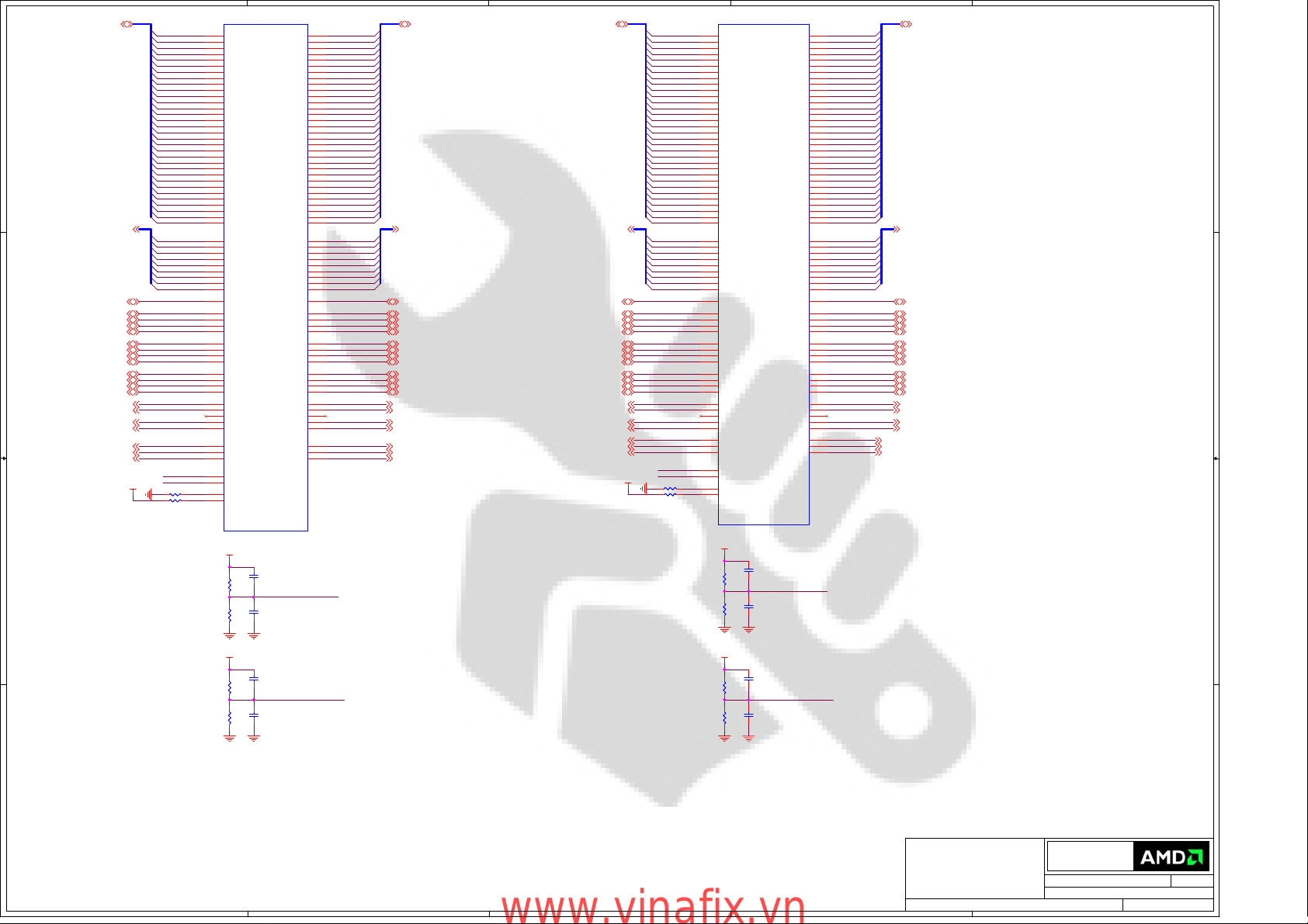
5
U1E
AA14
AA10
AA11
AA16
AA15
V10
V11
U11
U12
L11
M11
M10
W12
V14
V16
U13
V15
W13
W11
AA9
R10
R14
R13
P11
W14
P13
P12
U16
V17
E4
H4
G2
F6
J5
K6
K4
L1
M9
M6
M4
N3
N1
P6
R3
R1
R5
Y6
W3
Y4
W5
V4
U3
U5
U1
V9
L3
L5
T4
T6
H6
N5
W1
J3
R9
P4
V6
U1E
DQC0_0
DQC0_1
DQC0_2
DQC0_3
DQC0_4
DQC0_5
DQC0_6
DQC0_7
DQC0_8
DQC0_9
DQC0_10
DQC0_11
DQC0_12
DQC0_13
DQC0_14
DQC0_15
DQC0_16
DQC0_17
DQC0_18
DQC0_19
DQC0_20
DQC0_21
DQC0_22
DQC0_23
DQC0_24
DQC0_25
DQC0_26
DQC0_27
DQC0_28
DQC0_29
DQC0_30
DQC0_31
MAC0_0
MAC0_1
MAC0_2
MAC0_3
MAC0_4
MAC0_5
MAC0_6
MAC0_7
MAC0_8
ADBIC0
WCKC0_0
WCKC0B_0
WCKC0_1
WCKC0B_1
EDCC0_0
EDCC0_1
EDCC0_2
EDCC0_3
DDBIC0_0
DDBIC0_1
DDBIC0_2
DDBIC0_3
WEC0B
CSC0B_0
CSC0B_1
CASC0B
RASC0B
CKEC0
CLKC0
CLKC0B
MVREFCS
MVREFCD
MEM_CALRPC
MEM_CALRNC
DQC1_0
DQC1_1
DQC1_2
DQC1_3
DQC1_4
DQC1_5
DQC1_6
DQC1_7
DQC1_8
DQC1_9
DQC1_10
DQC1_11
DQC1_12
DQC1_13
DQC1_14
DQC1_15
DQC1_16
DQC1_17
DQC1_18
DQC1_19
DQC1_20
DQC1_21
DQC1_22
DQC1_23
DQC1_24
DQC1_25
DQC1_26
DQC1_27
DQC1_28
DQC1_29
DQC1_30
DQC1_31
MAC1_0
MAC1_1
MAC1_2
MAC1_3
MAC1_4
MAC1_5
MAC1_6
MAC1_7
MAC1_8
ADBIC1
WCKC1_0
WCKC1B_0
WCKC1_1
WCKC1B_1
EDCC1_0
EDCC1_1
EDCC1_2
EDCC1_3
DDBIC1_0
DDBIC1_1
DDBIC1_2
DDBIC1_3
WEC1B
CSC1B_0
CSC1B_1
CASC1B
RASC1B
CKEC1
CLKC1
CLKC1B
AR16
AN14
AR14
AR15
AM15
AM14
AK13
AK14
AJ15
AH12
AH13
AF10
AF9
AF16
AE13
AE12
AJ3
AJ1
AH4
AH6
AG1
AF4
AE5
AF6
AA5
AB4
AA3
AA1
AC5
AD6
AD4
AC3
AD9
AD11
AE11
AD14
AH11
AE14
AB13
AB14
AB11
AB12
AJ10
AJ11
AE3
AE1
AN13
AF11
AG5
AB6
AN12
AF12
AG3
AC1
AJ16
AF14
AF15
AD15
AD10
AD16
AJ14
AH14
DQC0_[31..0]9
D D
MAC0_[8..0]9
ADBIC09
WCKC0_09
WCKC0b_09
WCKC0_19
WCKC0b_19
C C
EDCC0_09
EDCC0_19
EDCC0_29
EDCC0_39
DDBIC0_09
DDBIC0_19
DDBIC0_29
DDBIC0_39
WEC0b9
CSC0b_09
CASC0b9
RASC0b9
CKEC09
CLKC09
CLKC0b9
+MVDDQ
DQC0_0
DQC0_1
DQC0_2
DQC0_3
DQC0_4
DQC0_5
DQC0_6
DQC0_7
DQC0_8
DQC0_9
DQC0_10
DQC0_11
DQC0_12
DQC0_13
DQC0_14
DQC0_15
DQC0_16
DQC0_17
DQC0_18
DQC0_19
DQC0_20
DQC0_21
DQC0_22
DQC0_23
DQC0_24
DQC0_25
DQC0_26
DQC0_27
DQC0_28
DQC0_29
DQC0_30
DQC0_31
MAC0_0
MAC0_1
MAC0_2
MAC0_3
MAC0_4
MAC0_5
MAC0_6
MAC0_7
MAC0_8
MVREFS_C
MVREFD_C
R135 243RR135 243R
R137 243RR137 243R
DQC1_0
DQC1_1
DQC1_2
DQC1_3
DQC1_4
DQC1_5
DQC1_6
DQC1_7
DQC1_8
DQC1_9
DQC1_10
DQC1_11
DQC1_12
DQC1_13
DQC1_14
DQC1_15
DQC1_16
DQC1_17
DQC1_18
DQC1_19
DQC1_20
DQC1_21
DQC1_22
DQC1_23
DQC1_24
DQC1_25
DQC1_26
DQC1_27
DQC1_28
DQC1_29
DQC1_30
DQC1_31
MAC1_0
MAC1_1
MAC1_2
MAC1_3
MAC1_4
MAC1_5
MAC1_6
MAC1_7
MAC1_8
4
DQC1_[31..0] 9
MAC1_[8..0] 9
ADBIC1 9
WCKC1_0 9
WCKC1b_0 9
WCKC1_1 9
WCKC1b_1 9
EDCC1_0 9
EDCC1_1 9
EDCC1_2 9
EDCC1_3 9
DDBIC1_0 9
DDBIC1_1 9
DDBIC1_2 9
DDBIC1_3 9
WEC1b 9
CSC1b_0 9
CASC1b 9
RASC1b 9
CKEC1 9
CLKC1 9
CLKC1b 9
3
U1F
AR11
AK12
AR10
AN11
AK11
AM11
AY10
AU11
AU10
AW12
AY12
BB10
BB11
AM10
AT13
AU14
AU15
AW13
AW11
AU16
AT12
AT11
AM17
AN17
AM16
AT14
AJ5
AK6
AK4
AL1
AM6
AM4
AN5
AN3
AR9
AJ9
AR3
AR1
AP6
AR5
AU1
AU3
AU5
AV2
BB6
BA5
BC1
BB4
AY6
AW5
AW3
AY4
BB9
AY9
AU9
AP2
AP4
AV4
AV6
AL3
AM9
AT4
BA3
AL5
AT6
BA1
U1F
DQD0_0
DQD0_1
DQD0_2
DQD0_3
DQD0_4
DQD0_5
DQD0_6
DQD0_7
DQD0_8
DQD0_9
DQD0_10
DQD0_11
DQD0_12
DQD0_13
DQD0_14
DQD0_15
DQD0_16
DQD0_17
DQD0_18
DQD0_19
DQD0_20
DQD0_21
DQD0_22
DQD0_23
DQD0_24
DQD0_25
DQD0_26
DQD0_27
DQD0_28
DQD0_29
DQD0_30
DQD0_31
MAD0_0
MAD0_1
MAD0_2
MAD0_3
MAD0_4
MAD0_5
MAD0_6
MAD0_7
MAD0_8
ADBID0
WCKD0_0
WCKD0B_0
WCKD0_1
WCKD0B_1
EDCD0_0
EDCD0_1
EDCD0_2
EDCD0_3
DDBID0_0
DDBID0_1
DDBID0_2
DDBID0_3
WED0B
CSD0B_0
CSD0B_1
CASD0B
RASD0B
CKED0
CLKD0
CLKD0B
MVREFDS
MVREFDD
MEM_CALRPD
MEM_CALRND
DQD1_0
DQD1_1
DQD1_2
DQD1_3
DQD1_4
DQD1_5
DQD1_6
DQD1_7
DQD1_8
DQD1_9
DQD1_10
DQD1_11
DQD1_12
DQD1_13
DQD1_14
DQD1_15
DQD1_16
DQD1_17
DQD1_18
DQD1_19
DQD1_20
DQD1_21
DQD1_22
DQD1_23
DQD1_24
DQD1_25
DQD1_26
DQD1_27
DQD1_28
DQD1_29
DQD1_30
DQD1_31
MAD1_0
MAD1_1
MAD1_2
MAD1_3
MAD1_4
MAD1_5
MAD1_6
MAD1_7
MAD1_8
ADBID1
WCKD1_0
WCKD1B_0
WCKD1_1
WCKD1B_1
EDCD1_0
EDCD1_1
EDCD1_2
EDCD1_3
DDBID1_0
DDBID1_1
DDBID1_2
DDBID1_3
WED1B
CSD1B_0
CSD1B_1
CASD1B
RASD1B
CKED1
CLKD1
CLKD1B
DQD0_[31..0]9
MAD0_[8..0]9
ADBID09
WCKD0_09
WCKD0b_09
WCKD0_19
WCKD0b_19
EDCD0_09
EDCD0_19
EDCD0_29
EDCD0_39
DDBID0_09
DDBID0_19
DDBID0_29
DDBID0_39
WED0b9
CSD0b_09
CASD0b9
RASD0b9
CKED09
CLKD09
CLKD0b9
+MVDDQ
DQD0_0
DQD0_1
DQD0_2
DQD0_3
DQD0_4
DQD0_5
DQD0_6
DQD0_7
DQD0_8
DQD0_9
DQD0_10
DQD0_11
DQD0_12
DQD0_13
DQD0_14
DQD0_15
DQD0_16
DQD0_17
DQD0_18
DQD0_19
DQD0_20
DQD0_21
DQD0_22
DQD0_23
DQD0_24
DQD0_25
DQD0_26
DQD0_27
DQD0_28
DQD0_29
DQD0_30
DQD0_31
MAD0_0
MAD0_1
MAD0_2
MAD0_3
MAD0_4
MAD0_5
MAD0_6
MAD0_7
MAD0_8
MVREFS_D
MVREFD_D
R134 243RR134 243R
R136 243RR136 243R
BC18
BB18
BA18
AY18
BE17
BA15
BB15
BD14
BH12
BK12
BN11
BL11
BH14
BK14
BM14
BN13
BJ11
BK10
BM7
BL9
BH10
BH8
BH6
BL3
BC5
BD4
BC3
BF1
BD6
BF6
BF4
BG2
BD11
BE12
AY14
BD12
BC15
BC14
BC9
BD10
BC11
BE10
BL15
BJ15
BK5
BJ4
BD17
BJ13
BJ9
BE3
BC17
BL13
BK8
BE5
AV17
AW15
AY15
BD9
BE14
BB12
AY17
AW17
2
DQD1_0
DQD1_1
DQD1_2
DQD1_3
DQD1_4
DQD1_5
DQD1_6
DQD1_7
DQD1_8
DQD1_9
DQD1_10
DQD1_11
DQD1_12
DQD1_13
DQD1_14
DQD1_15
DQD1_16
DQD1_17
DQD1_18
DQD1_19
DQD1_20
DQD1_21
DQD1_22
DQD1_23
DQD1_24
DQD1_25
DQD1_26
DQD1_27
DQD1_28
DQD1_29
DQD1_30
DQD1_31
MAD1_0
MAD1_1
MAD1_2
MAD1_3
MAD1_4
MAD1_5
MAD1_6
MAD1_7
MAD1_8
MAD1_[8..0] 9
ADBID1 9
WCKD1_0 9
WCKD1b_0 9
WCKD1_1 9
WCKD1b_1 9
EDCD1_0 9
EDCD1_1 9
EDCD1_2 9
EDCD1_3 9
DDBID1_0 9
DDBID1_1 9
DDBID1_2 9
DDBID1_3 9
WED1b 9
CSD1b_0 9
CASD1b 9
RASD1b 9
CKED1 9
CLKD1 9
CLKD1b 9
1
DQD1_[31..0] 9
RV770 GL A11
RV770 GL A11
RV770 GL A11
+MVDDQ
B B
A A
5
+MVDDQ
R139
R139
40.2R
40.2R
1%
R141
R141
100R
100R
1%
R143
R143
40.2R
40.2R
1%
R145
R145
100R
100R
1%
C311
C311
1uF_6.3V
1uF_6.3V
C315
C315
1uF_6.3V
1uF_6.3V
C319
C319
1uF_6.3V
1uF_6.3V
C323
C323
1uF_6.3V
1uF_6.3V
MVREFD_C
MVREFD/S =0.7*
VDDR1
(GDDR3/4/5)
MVREFS_C
4
www.vinafix.vn
3
RV770 GL A11
+MVDDQ
+MVDDQ
R138
R138
40.2R
40.2R
1%
R140
R140
100R
100R
1%
R142
R142
40.2R
40.2R
1%
R144
R144
100R
100R
1%
C309
C309
1uF_6.3V
1uF_6.3V
C313
C313
1uF_6.3V
1uF_6.3V
C317
C317
1uF_6.3V
1uF_6.3V
C321
C321
1uF_6.3V
1uF_6.3V
MVREFD_D
MVREFD/S =0.7*
VDDR1
(GDDR3/4/5)
MVREFS_D
CONFIDENTIAL & PROPRIETARY TO ADVANCED MICRO DEVICES INC.
CONFIDENTIAL & PROPRIETARY TO ADVANCED MICRO DEVICES INC.
CONFIDENTIAL & PROPRIETARY TO ADVANCED MICRO DEVICES INC.
?2007 Advanced Micro Devices
?2007 Advanced Micro Devices
?2007 Advanced Micro Devices
This AMD Board schematic and design is the exclusive property of AMD,
This AMD Board schematic and design is the exclusive property of AMD,
This AMD Board schematic and design is the exclusive property of AMD,
and is provided only to entities under a non-disclosure agreement
and is provided only to entities under a non-disclosure agreement
and is provided only to entities under a non-disclosure agreement
with AMD for evaluation purposes. Further distribution or disclosure
with AMD for evaluation purposes. Further distribution or disclosure
with AMD for evaluation purposes. Further distribution or disclosure
is strictly prohibited. Use of this schematic and design for any purpose
is strictly prohibited. Use of this schematic and design for any purpose
is strictly prohibited. Use of this schematic and design for any purpose
other than evaluation requires a Board Technology License Agreement
other than evaluation requires a Board Technology License Agreement
other than evaluation requires a Board Technology License Agreement
with AMD. AMD makes no representations or warranties of any kind
with AMD. AMD makes no representations or warranties of any kind
with AMD. AMD makes no representations or warranties of any kind
regarding this schematic and design, including, not limited to,
regarding this schematic and design, including, not limited to,
regarding this schematic and design, including, not limited to,
any implied warranty of merchantibility or fitness for a particular
any implied warranty of merchantibility or fitness for a particular
any implied warranty of merchantibility or fitness for a particular
purpose, and disclaims responsibility forany consequences resulting
purpose, and disclaims responsibility forany consequences resulting
purpose, and disclaims responsibility forany consequences resulting
from use of the information included herein.
from use of the information included herein.
from use of the information included herein.
Title
Title
2
Title
RH RV770 GDDR5 DVI-I VO DVI-I FH
RH RV770 GDDR5 DVI-I VO DVI-I FH
RH RV770 GDDR5 DVI-I VO DVI-I FH
Advanced Micro Devices Inc.
Advanced Micro Devices Inc.
Advanced Micro Devices Inc.
1 Commerce Valley Drive East
1 Commerce Valley Drive East
1 Commerce Valley Drive East
Markham, Ontario
Markham, Ontario
Markham, Ontario
Wednesday, December 10, 2008
Wednesday, December 10, 2008
Wednesday, December 10, 2008
Sheet
Sheet
Sheet
of
622
of
622
of
622
1
Doc No.
Doc No.
Doc No.
RevDate:
RevDate:
RevDate:
2
2
2
105-B507xx-11
105-B507xx-11
105-B507xx-11
Page 7
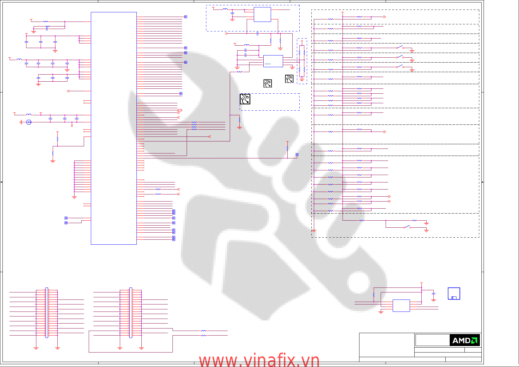
5
U1K
U1K
+1.8V
R147 221RR147 221R
R151 110RR151 110R
C328 100nF_6.3VC328 100nF_6.3V
+3.3V
C333
C333
C332
C332
100nF_6.3V
100nF_6.3V
100nF_6.3V
B113
B113
BLM15BD121SN1
BLM15BD121SN1
+1.8V
B119
B119
1 2
100nF_6.3V
C325
C325
10uF_X6S
10uF_X6S
NS8NS_VIA NS8NS_VIA
+TSVDD
C335
C335
1uF_6.3V
1uF_6.3V
C329
C329
1uF_6.3V
1uF_6.3V
1uF_6.3V
1uF_6.3V
C365
C365
D D
+1.8V
BLM15BD121SN1
BLM15BD121SN1
C C
B B
TS_FDO19
100nF_6.3V
100nF_6.3V
DNI
C334
C334
100nF_6.3V
100nF_6.3V
C326
C326
100nF_6.3V
100nF_6.3V
C330
C330
100nF_6.3V
100nF_6.3V
C366
C366
+3.3V
MR170
MR170
10K
10K
R1701KR170
1K
TP4008
TP4008
TP4009
TP4009
VREFG
C327
C327
1uF_6.3V
1uF_6.3V
C331
C331
1uF_6.3V
1uF_6.3V
C367
C367
10nF
10nF
GND_TSVSS
JTAG_MODE
35mil
35mil
35mil
35mil
BG21
AU29
AU30
AU32
AU33
BB24
BE24
BC24
BD24
BE25
BD25
BB25
BC25
AV36
AV30
AW30
AU24
AU25
BA30
BB30
AU39
BG19
BA22
AV28
BA29
BA35
AW36
BA26
AY30
BM22
BN19
AU22
BG43
AU28
AU26
AR19
AP19
BA19
AY19
VREFG
VDDR3#1
VDDR3#2
VDDR3#3
VDDR3#4
VDDR5#1
VDDR5#2
VDDR5#3
VDDR5#4
VDDR4#1
VDDR4#2
VDDR4#3
VDDR4#4
TS_FDO
DPLUS
DMINUS
TSVDD
TSVSS
RSVD#1
RSVD#2
JMODE
VSSD#1
VSSD#2
VSSD#3
VSSD#4
VSSD#5
VSSD#6
VSSD#7
VSSD#8
VSSD#9
VSSD#10
VSSD#11
VSSD#12
VSSD#13
VSSD#14
NC_GPIO_31
NC_GPIO_32
TEST_YCLK
TEST_MCLK
RV770 GL A11
RV770 GL A11
DVPDATA_0
DVPDATA_1
DVPDATA_2
DVPDATA_3
DVPDATA_4
DVPDATA_5
DVPDATA_6
DVPDATA_7
DVPDATA_8
DVPDATA_9
DVPDATA_10
DVPDATA_11
DVPCLK
DVPCNTL_0
DVPCNTL_1
DVPCNTL_2
DVPDATA_12
DVPDATA_13
DVPDATA_14
DVPDATA_15
DVPDATA_16
DVPDATA_17
DVPDATA_18
DVPDATA_19
DVPDATA_20
DVPDATA_21
DVPDATA_22
DVPDATA_23
DVPCNTL_MVP_0
DVPCNTL_MVP_1
GPIO_0
GPIO_1
GPIO_2
GPIO_3_SMBDAT
GPIO_4_SMBCLK
GPIO_5
GPIO_6_TACH
GPIO_7
GPIO_8_ROMSO
GPIO_9_ROMSI
GPIO_10_ROMSCK
GPIO_11
GPIO_12
GPIO_13
GPIO_14_HPD2
GPIO_15_PWRCNTL_0
GPIO_16_SSIN
GPIO_17_THERMAL_INT
GPIO_18_HPD3
GPIO_19_CTF
GPIO_20_PWRCNTL_1
GPIO_21
GPIO_22_ROMCSB
GPIO_23_CLKREQB
GPIO_24_TRSTB
GPIO_25_TDI
GPIO_26_TCK
GPIO_27_TMS
GPIO_28_TDO
GENERICA
GENERICB
GENERICC
GENERICD
GENERICE
GENERICF
GENERICG
GENERICH
VPCLK0
DVALID
VHAD_0
VHAD_1
VPHCTL
VIPCLK
VIP_0
VIP_1
VIP_2
VIP_3
VIP_4
VIP_5
VIP_6
VIP_7
PSYNC
BH20
BK20
BM20
BJ21
BL21
BN21
BH22
BK22
BG23
BJ23
BN23
BL23
BK18
BM18
BJ19
BL19
AW25
AY24
AV25
AY25
AY26
AW26
BA28
AV26
AY28
AW28
AY29
AW29
AW24
AV24
BA24
AV29
BH24
BD22
BA25
BE22
AY22
BC22
BB22
BA21
BB21
AW22
BE21
BD21
BD19
BB19
BC19
BE19
AY21
BH18
BN17
BG17
BC21
AW21
BL17
BM16
BH16
BK16
BJ17
BC35
BE32
BC33
BA33
BC30
BD35
BB29
BD32
AV35
AW35
AY35
AV33
AW33
AY33
AV32
AW32
AY32
BB33
BE35
AU36
AU35
BB35
BA32
4
DVPDATA_0
DVPDATA_1
DVPDATA_2
DVPDATA_3
DVPDATA_4
DVPDATA_5
DVPDATA_6
DVPDATA_7
DVPDATA_8
DVPDATA_9
DVPDATA_10
DVPDATA_11
DVOCLK
DVPCNTL_0
DVPCNTL_1
DVPCNTL_2
DVPDATA_12
DVPDATA_13
DVPDATA_14
DVPDATA_15
DVPDATA_16
DVPDATA_17
DVPDATA_18
DVPDATA_19
DVPDATA_20
DVPDATA_21
DVPDATA_22
DVPDATA_23
DVP_MVP_CNTL_0
DVP_MVP_CNTL_1
GPIO_0
GPIO_1
GPIO_2
GPIO_3
GPIO_4
GPIO_6
GPIO_7
GPIO_8
GPIO_9
GPIO_10
GPIO_11
GPIO_12
GPIO_13
HPD2
GPIO_16
GPIO_21
GPIO_22_ROMCSb
PCIE_CLK_REQb
GENERICB
GENERICC
GENERICD
R198 0RR198 0R
R204 0RR204 0R
VIP_0
VIP_1
VIP_2
VIP_3
VIP_6
DVALIDDVALID
PSYNCPSYNC
VHAD_0
TP400535mil TP400535mil
CrossFire
TP400335mil TP400335mil
TP400435mil TP400435mil
TP400635mil TP400635mil
TP4007
TP4007
DVP_MVP_CNTL_0 : DE for bits D[12..23]
35mil
35mil
DVP_MVP_CNTL_1 : CLK for bits D[12..23]
FLOW_CONTROL_1 - Lower Cable
GPIO_3 1
FLOW_CONTROL_2 - Upper Cable
GPIO_4 1
SWAP_LOCK_1 - Lower Cable
SWAP_LOCK_2 - Upper Cable
TACH 19
EXT_12V_DET 17
EXT_12V_DET_B 17
TP401135mil TP401135mil
TP401235mil TP401235mil
TP401335mil TP401335mil
TP401735mil TP401735mil
TP401635mil TP401635mil
TP401035mil TP401035mil
TP401435mil TP401435mil
TP401535mil TP401535mil
+1.8V
BLM15BD121SN1
BLM15BD121SN1
B125
B125
100nF_6.3V
100nF_6.3V
1.8V to 3.3V translator option
SSCLKIN3
CrossFire
GPIO_8_R
RP1A33R RP1A33R
81
GPIO_9_R
RP1B33R RP1B33R
72
GPIO_10_R
RP1C33R RP1C33R
63
ROMCSb_R
RP1D33R RP1D33R
54
HPD2 16
C398
C398
3
+3.3V
BLM15BD121SN1
BLM15BD121SN1
B124
B124
C397 1uF_6.3VC397 1uF_6.3V
C395 100nF_6.3VC395 100nF_6.3V
R197 0RR197 0R
Share pad
R203
R203
150R
150R
Place close to U1
GPIOs for VDDC Setting
U14
U14
1
VCCA
5
DIR
2
GND
A3B
DIGPOT_10K
DIGPOT_10K
C396
C396
10nF_25V
10nF_25V
SS_VCC
8
7
6
5
Place SW1 & SW2 on the bottom side
(easily accessible).
Clearly Mark A & B contacts on the
silkscreen.
VCCB
VCC
CRSEL
SSO
SSEN
6
4
R201
R201
100K
100K
CLKIN
SMSEL1
SMSEL2
GND
DS1081LE
DS1081LE
SS_VCC
U13
U13
R202
R202
100K
100K
1
2
3
4
+3.3V
TR1
TR1
10K
10K
2
+3.3V
R146 10KR146 10K
R150 10KR150 10K
DNI
R148 10KR148 10K
R149 10KR149 10K
R152 10KR152 10K
R153 10KR153 10K
DNI
R155 10KR155 10K
DNI
R156 10KR156 10K
R157 10KR157 10K
DNI
R158 10KR158 10K
R159 10KR159 10K
R160 10KR160 10K
R161 10KR161 10K
Stuff R161 for HDMI connector
DNI
R163 10KR163 10K
DNI
R164 10KR164 10K
DNI
R165 10KR165 10K
DNI
R166 10KR166 10K
DNI
R167 10KR167 10K
DNI
R168 10KR168 10K
DNI
R169 10KR169 10K
DNI
R173 10KR173 10K
DNI
R175 10KR175 10K
NTSC
R176 10KR176 10K
Share padPlace close to U13
35mil
35mil
+3.3V
R200 0RR200 0R
MR200 0RMR200 0R
TP29
TP29
DNI
MR146 10KMR146 10K
DNI
MR150 10KMR150 10K
MR148 10KMR148 10K
DNI
MR149 10KMR149 10K
R199 0RR199 0R
DNI
MR152 10KMR152 10K
DNI
MR153 10KMR153 10K
MR199 0RMR199 0R
DNI
DNI
DNI
MR155 10KMR155 10K
MR156 10KMR156 10K
MR157 10KMR157 10K
MR158 10KMR158 10K
MR159 10KMR159 10K
MR160 10KMR160 10K
MR161 10KMR161 10K
MR163 10KMR163 10K
MR164 10KMR164 10K
MR165 10KMR165 10K
MR166 10KMR166 10K
MR167 10KMR167 10K
MR168 10KMR168 10K
MR169 10KMR169 10K
MR173 10KMR173 10K
MR175 10KMR175 10K
Pull-Down Resistors are for BU until built-in pull-downs are verified.
PIN BASED STRAPS
VSYNC1 3,15
VSYNC
VHAD_0
PSYNC
GPIO_0
GPIO_1
GPIO_2
VIP_1
GPIO_9_R
GPIO_13
GPIO_12
GPIO_11
GPIO_8
HSYNC1 3,15
HSYNC1
DVALID
VIP_6
VIP_3
VIP_2
VIP_0
GPIO_21
VSYNC2
HSYNC2
GENERICC
GPIO_7
SW1A
SW1A
41
DIP_SWX2
DIP_SWX2
SW1B
SW1B
32
DIP_SWX2
DIP_SWX2
SW2A
SW2A
41
DIP_SWX2
DIP_SWX2
VSYNC2 3,16
HSYNC2 3,16
BUO
SW2B
SW2B
DIP_SWX2
DIP_SWX2
1
VIP_DEVICE_STRAP_EN
0: Slave VIP host port devices present (use if Theater is populated)
1: No slave VIP host port devices reporting presence during reset (use for
configurations without video-in)
If VIP_DEVICE_STRAP_EN is set to ?? then this pin is
used to sense whether a VIP slave device is connected to
the VIP Host interface. If VIP_DEVICE_STRAP_EN is set
to ?? then this pin is not used as a strap at all
VGA DISABLE : 1 for disable (set to 0 for normal operation)
GPIO(0) - TX_PWRS_ENB (Transmitter Power Savings Enable)
0: 50% Tx output swing for mobile mode
1: full Tx output swing (Default setting for Desktop)
GPIO(1) - TX_DEEMPH_EN (Transmitter De-emphasis Enable)
0: Tx de-emphasis disabled for mobile mode
1: Tx de-emphasis enabled (Default setting for Desktop)
GPIO(2) - BIF_GEN2_EN (5.0 GT/s Enable)
1 : Allows either PCIe 2.5 GT/s or 5.0 GT/s operation
0 : Debug use only (disables PCIe 5.0 GT/s negotiation)
MSI_DIS (Default: 0)
Disable Message Signaled Interrupt is both a ROM strap
and a pin strap. The pin strap is only applicable if a BIOS
ROM is not present.
GPIO(9,13, 12,11) - CONFIG[3..0]
CONFIG[3]
0100 - 512Kbit M25P05A (ST)
0101 - 1Mbit M25P10A (ST)
CONFIG[2]
0101 - 2Mbit M25P20 (ST)
0101 - 4Mbit M25P40 (ST)
CONFIG[1]
0101 - 8Mbit M25P80 (ST)
0100 - 512Kbit Pm25LV512 (Chingis)
CONFIG[0]
0101 - 1Mbit Pm25LV010 (Chingis)
AUDIO_EN : Enable HD Audio function in the PCI configuration space.
0 - Disable HD Audio
1 - Enable HD Audio
HD audio must only be enabled on systems that are legally
entitled. It is the responsibility of the system designer to
ensure that the system is entitled to support this feature.
HDMI_EN :
Note: Board manufacturer must not set this strap to 1 unless
there is an onboard HDMI connector. It is the
manufacturers responsibility to pay royalties if this strap is
enabled.
This Board doesn't have HDMI Connector
therefore only pull down option is available
BIF_CLK_PM_EN
0 - Disable CLKREQ# power management capability
1 - Enable CLKREQ# power management capability
RESERVED :Internal use only. Other logic must not affect this signal
during RESET.
MR176 10KMR176 10K
32
1 - NTSC TVO0 - PAL TVO TV OUT STANDARD
CrossFire Card-Edge
Lower Cable Card Edge
1
DVOCLK
DVPCNTL_2
DVPDATA_1
DVPDATA_3
DVPDATA_5
DVPDATA_7
A A
DVPDATA_9
DVPDATA_11
DVPCNTL_1
GENERICD
3
5
7
9
11
13
15
17
19
21
23
25
27
29 30
31
33
35
37
39
J1J1
2
4
6
8
DVPDATA_0
10
12
DVPDATA_2
14
16
DVPDATA_4
18
20
DVPDATA_6
22
24
DVPDATA_8
26
28
DVPDATA_10
32
DVPCNTL_0
34
36
GPIO_2
38
40
Bundle B
5
Upper Cable Card Edge
1
DVP_MVP_CNTL_1
DVP_MVP_CNTL_0
DVPDATA_13
DVPDATA_15
DVPDATA_17
DVPDATA_19
DVPDATA_21
DVPDATA_23
GENERICB_R
GENERICC
3
5
7
9
11
13
15
17
19
21
23
25
27
29 30
31
33
35
37
39
J2J2
2
4
6
8
DVPDATA_12
10
12
DVPDATA_14
14
16
DVPDATA_16
18
20
DVPDATA_18
22
24
DVPDATA_20
26
28
DVPDATA_22
32
DVALID_R
34
36
GPIO_1
38
40
Bundle A (closer to the bracket)
4
DNI
R181 0RR181 0R
R182 0RR182 0R
GENERICB: Generic I2C_SDA
DVALID: Generic I2C_SCL
DVALID
DNI
GENERICB
www.vinafix.vn
3
ROMCSb_R
GPIO_8_R
R180
R180
10K
10K
U2
U2
1
CE#
VCC
2
SO
HOLD#
3
WP#
SCK
GND4SI
PM25LV010-25SCE
PM25LV010-25SCE
+3.3V
8
7
GPIO_10_R
6
GPIO_9_R
5
C342
C342
100nF_6.3V
100nF_6.3V
BIOS1
BIOS1
BIOS
BIOS
113-B339XX-XXX
113-B339XX-XXX
VIDEO BIOS
FIRMWARE
PN 2280007900G for 1Mbit (PM25LV010A-100SCE)
CONFIDENTIAL & PROPRIETARY TO ADVANCED MICRO DEVICES INC.
CONFIDENTIAL & PROPRIETARY TO ADVANCED MICRO DEVICES INC.
CONFIDENTIAL & PROPRIETARY TO ADVANCED MICRO DEVICES INC.
?2007 Advanced Micro Devices
?2007 Advanced Micro Devices
?2007 Advanced Micro Devices
This AMD Board schematic and design is the exclusive property of AMD,
This AMD Board schematic and design is the exclusive property of AMD,
This AMD Board schematic and design is the exclusive property of AMD,
and is provided only to entities under a non-disclosure agreement
and is provided only to entities under a non-disclosure agreement
and is provided only to entities under a non-disclosure agreement
with AMD for evaluation purposes. Further distribution or disclosure
with AMD for evaluation purposes. Further distribution or disclosure
with AMD for evaluation purposes. Further distribution or disclosure
is strictly prohibited. Use of this schematic and design for any purpose
is strictly prohibited. Use of this schematic and design for any purpose
is strictly prohibited. Use of this schematic and design for any purpose
other than evaluation requires a Board Technology License Agreement
other than evaluation requires a Board Technology License Agreement
other than evaluation requires a Board Technology License Agreement
with AMD. AMD makes no representations or warranties of any kind
with AMD. AMD makes no representations or warranties of any kind
with AMD. AMD makes no representations or warranties of any kind
regarding this schematic and design, including, not limited to,
regarding this schematic and design, including, not limited to,
regarding this schematic and design, including, not limited to,
any implied warranty of merchantibility or fitness for a particular
any implied warranty of merchantibility or fitness for a particular
any implied warranty of merchantibility or fitness for a particular
purpose, and disclaims responsibility forany consequences resulting
purpose, and disclaims responsibility forany consequences resulting
purpose, and disclaims responsibility forany consequences resulting
from use of the information included herein.
from use of the information included herein.
from use of the information included herein.
Title
Title
Title
RH RV770 GDDR5 DVI-I VO DVI-I FH
RH RV770 GDDR5 DVI-I VO DVI-I FH
2
RH RV770 GDDR5 DVI-I VO DVI-I FH
Advanced Micro Devices Inc.
Advanced Micro Devices Inc.
Advanced Micro Devices Inc.
1 Commerce Valley Drive East
1 Commerce Valley Drive East
1 Commerce Valley Drive East
Markham, Ontario
Markham, Ontario
Markham, Ontario
Friday, December 12, 2008
Friday, December 12, 2008
Friday, December 12, 2008
Sheet
Sheet
Sheet
of
722
of
722
of
722
1
Doc No.
Doc No.
Doc No.
RevDate:
RevDate:
RevDate:
2
2
2
105-B507xx-11
105-B507xx-11
105-B507xx-11
Page 8

DQA0_[31..0]5
D D
MAA0_[8..0]5 MAA1_[8..0]5 MAB0_[8..0]5 MAB1_[8..0]5
C C
R1213 120RR1213 120R
R1217 0RR1217 0R
R1221 0R DNIR1221 0R DNI
+MVDDQ
DRAM_RST5,9
B B
+MVDDQ
+MVDDQ
+MVDDQ
C1205 1uF_6.3VC1205 1uF_6.3V
R1233 2.37KR1233 2.37K
R1237 5.49KR1237 5.49K
C1201 1uF_6.3VC1201 1uF_6.3V
C1213 1uF_6.3VC1213 1uF_6.3V
R1241 2.37KR1241 2.37K
R1245 5.49KR1245 5.49K
C1209 1uF_6.3VC1209 1uF_6.3V
C1221 1uF_6.3VC1221 1uF_6.3V
1%
R1253 5.49KR1253 5.49K
C1217 1uF_6.3VC1217 1uF_6.3V
5
GDDR5
SEN_A0
MF_A0
U3
M2
DQ31 | DQ7
M4
DQ30 | DQ6
N2
DQ29 | DQ5
N4
DQ28 | DQ4
T2
DQ27 | DQ3
T4
DQ26 | DQ2
V2
DQ25 | DQ1
V4
DQ24 | DQ0
M13
DQ23 | DQ15
M11
DQ22 | DQ14
N13
DQ21 | DQ13
N11
DQ20 | DQ12
T13
DQ19 | DQ11
T11
DQ18 | DQ10
V13
DQ17 | DQ9
V11
DQ16 | DQ8
F13
DQ15 | DQ23
F11
DQ14 | DQ22
E13
DQ13 | DQ21
E11
DQ12 | DQ20
B13
DQ11 | DQ19
B11
DQ10 | DQ18
A13
DQ9 | DQ17
A11
DQ8 | DQ16
F2
DQ7 | DQ31
F4
DQ6 | DQ30
E2
DQ5 | DQ29
E4
DQ4 | DQ28
B2
DQ3 | DQ27
B4
DQ2 | DQ26
A2
DQ1 | DQ25
A4
DQ0 | DQ24
J5
RFU/A12/NC
K4
A7/A8 | A0/A10
K5
A6/A11 | A1/A9
K10
A5/BA1 | A3/BA3
K11
A4/BA2 | A2/BA0
H10
A3/BA3 | A5/BA1
H11
A2 /BA0 | A4/BA2
H5
A1/A9 | A6/A11
H4
A0/A10 | A7/A8
D4
WCK01 | WCK23
D5
WCK01# | WCK23#
P4
WCK23 | WCK01
P5
WCK23# | WCK01#
R2
EDC3 | EDC0
R13
EDC2 | EDC1
C13
EDC1 | EDC2
C2
EDC0 | EDC3
P2
DBI3# | DBI0#
P13
DBI2 #| DBI1#
D13
DBI1# | DBI2#
D2
DBI0# | DBI3#
G3
RAS# | CAS#
L3
CAS# | RAS#
J3
CKE#
J11
CK#
J12
CK
G12
CS# | WE#
L12
WE# | CS#
J13
ZQ
J10
SEN
J2
RESET#
J1
MF
A5
Vpp,NC
V5
Vpp,NC1
A10
VREFD1
V10
VREFD2
J14
VREFC
J4
ABI#
GDDR5U3GDDR5
VDDQ-B1
VDDQ-B3
VDDQ-B12
VDDQ-B14
VDDQ-D1
VDDQ-D3
VDDQ-D12
VDDQ-D14
VDDQ-E5
VDDQ-E10
VDDQ-F1
VDDQ-F3
VDDQ-F12
VDDQ-F14
VDDQ-G2
VDDQ-G13
VDDQ-H3
VDDQ-H12
VDDQ-K3
VDDQ-K12
VDDQ-L2
VDDQ-L13
VDDQ-M1
VDDQ-M3
VDDQ-M12
VDDQ-M14
VDDQ-N5
VDDQ-N10
VDDQ-P1
VDDQ-P3
VDDQ-P12
VDDQ-P14
VDDQ-T1
VDDQ-T3
VDDQ-T12
VDDQ-T14
VDD-C5
VDD-C10
VDD-D11
VDD-G1
VDD-G4
VDD-G11
VDD-G14
VDD-L1
VDD-L4
VDD-L11
VDD-L14
VDD-P11
VDD-R5
VDD-R10
VSSQ-A1
VSSQ-A3
VSSQ-A12
VSSQ-A14
VSSQ-C1
VSSQ-C3
VSSQ-C4
VSSQ-C11
VSSQ-C12
VSSQ-C14
VSSQ-E1
VSSQ-E3
VSSQ-E12
VSSQ-E14
VSSQ-F5
VSSQ-F10
VSSQ-H2
VSSQ-H13
VSSQ-K2
VSSQ-K13
VSSQ-M5
VSSQ-M10
VSSQ-N1
VSSQ-N3
VSSQ-N12
VSSQ-N14
VSSQ-R1
VSSQ-R3
VSSQ-R4
VSSQ-R11
VSSQ-R12
VSSQ-R14
VSSQ-V1
VSSQ-V3
VSSQ-V12
VSSQ-V14
VSS-B5
VSS-B10
VSS-D10
VSS-G5
VSS-G10
VSS-H1
VSS-H14
VSS-K1
VSS-K14
VSS-L5
VSS-L10
VSS-P10
VSS-T5
VSS-T10
B1
B3
B12
B14
D1
D3
D12
D14
E5
E10
F1
F3
F12
F14
G2
G13
H3
H12
K3
K12
L2
L13
M1
M3
M12
M14
N5
N10
P1
P3
P12
P14
T1
T3
T12
T14
+MVDDC
C5
C10
D11
G1
G4
G11
G14
L1
L4
L11
L14
P11
R5
R10
A1
A3
A12
A14
C1
C3
C4
C11
C12
C14
E1
E3
E12
E14
F5
F10
H2
H13
K2
K13
M5
M10
N1
N3
N12
N14
R1
R3
R4
R11
R12
R14
V1
V3
V12
V14
B5
B10
+MVDDQ
D10
G5
G10
H1
H14
+MVDDQ
K1
K14
L5
L10
P10
T5
+MVDDQ
T10
DQA0_13
DQA0_14
DQA0_15
DQA0_12
DQA0_10
DQA0_8
DQA0_11
DQA0_9
DQA0_7
DQA0_1
DQA0_6
DQA0_3
DQA0_2
DQA0_4
DQA0_0
DQA0_5
DQA0_21
DQA0_20
DQA0_23
DQA0_22
DQA0_17
DQA0_19
DQA0_18
DQA0_16
DQA0_29
DQA0_31
DQA0_28
DQA0_30
DQA0_25
DQA0_27
DQA0_26
DQA0_24
+MVDDQ
R1201 60.4RR1201 60.4R
CLKA05
R1205 60.4RR1205 60.4R
CLKA0b5
MAA0_8
MAA0_7
MAA0_6
MAA0_5
MAA0_4
MAA0_3
MAA0_2
MAA0_1
MAA0_0
WCKA0_15
WCKA0b_15
WCKA0_05
WCKA0b_05
EDCA0_15
EDCA0_05
EDCA0_25
EDCA0_35
DDBIA0_15
DDBIA0_05
DDBIA0_25
DDBIA0_35
RASA0b5
CASA0b5
CKEA05 CKEA15
CLKA0b
CLKA0
CSA0b_05
WEA0b5
1%
VREFD1_A0
1%
1%
1%
VREFD2_A0
1%
1%
VREFC_A0
1%
ADBIA05
4
DQA1_[31..0]5
DRAM_RST5,9
C1206 1uF_6.3VC1206 1uF_6.3V
R1234 2.37KR1234 2.37K
R1238 5.49KR1238 5.49K
C1202 1uF_6.3VC1202 1uF_6.3V
C1214 1uF_6.3VC1214 1uF_6.3V
R1242 2.37KR1242 2.37K
R1246 5.49KR1246 5.49K
C1210 1uF_6.3VC1210 1uF_6.3V
C1222 1uF_6.3VC1222 1uF_6.3V
1%
R1250 2.37KR1250 2.37K
R1254 5.49KR1254 5.49K
C1218 1uF_6.3VC1218 1uF_6.3V
DQA1_28
DQA1_29
DQA1_31
DQA1_30
DQA1_25
DQA1_27
DQA1_24
DQA1_26
DQA1_23
DQA1_21
DQA1_22
DQA1_20
DQA1_18
DQA1_17
DQA1_19
DQA1_16
DQA1_6
DQA1_5
DQA1_4
DQA1_7
DQA1_0
DQA1_1
DQA1_2
DQA1_3
DQA1_11
DQA1_10
DQA1_13
DQA1_8
DQA1_14
DQA1_12
DQA1_9
DQA1_15
+MVDDQ +MVDDQ +MVDDQ
R1202 60.4RR1202 60.4R
CLKA15
R1206 60.4RR1206 60.4R
CLKA1b5
MAA1_8
MAA1_0
MAA1_1
MAA1_3
MAA1_2
MAA1_5
MAA1_4
MAA1_6
MAA1_7
WCKA1_05
WCKA1b_05
WCKA1_15
WCKA1b_15
EDCA1_35
EDCA1_25
EDCA1_05
EDCA1_15
DDBIA1_35
DDBIA1_25
DDBIA1_05
DDBIA1_15
CASA1b5
RASA1b5
WEA1b5
CSA1b_05
R1214 120RR1214 120R
1%
G1_SEN_A1
R1218 0RR1218 0R
R1222 0R DNIR1222 0R DNI
+MVDDQ
VREFD1_A1
1%
1%
1%
VREFD2_A1
1%
1%
VREFC_A1
VREFC_A1
1%
ADBIA15 ADBIB15
CLKA1b
CLKA1
U4
M2
DQ31 | DQ7
M4
DQ30 | DQ6
N2
DQ29 | DQ5
N4
DQ28 | DQ4
T2
DQ27 | DQ3
T4
DQ26 | DQ2
V2
DQ25 | DQ1
V4
DQ24 | DQ0
M13
DQ23 | DQ15
M11
DQ22 | DQ14
N13
DQ21 | DQ13
N11
DQ20 | DQ12
T13
DQ19 | DQ11
T11
DQ18 | DQ10
V13
DQ17 | DQ9
V11
DQ16 | DQ8
F13
DQ15 | DQ23
F11
DQ14 | DQ22
E13
DQ13 | DQ21
E11
DQ12 | DQ20
B13
DQ11 | DQ19
B11
DQ10 | DQ18
A13
DQ9 | DQ17
A11
DQ8 | DQ16
F2
DQ7 | DQ31
F4
DQ6 | DQ30
E2
DQ5 | DQ29
E4
DQ4 | DQ28
B2
DQ3 | DQ27
B4
DQ2 | DQ26
A2
DQ1 | DQ25
A4
DQ0 | DQ24
J5
RFU/A12/NC
K4
A7/A8 | A0/A10
K5
A6/A11 | A1/A9
K10
A5/BA1 | A3/BA3
K11
A4/BA2 | A2/BA0
H10
A3/BA3 | A5/BA1
H11
A2 /BA0 | A4/BA2
H5
A1/A9 | A6/A11
H4
A0/A10 | A7/A8
D4
WCK01 | WCK23
D5
WCK01# | WCK23#
P4
WCK23 | WCK01
P5
WCK23# | WCK01#
R2
EDC3 | EDC0
R13
EDC2 | EDC1
C13
EDC1 | EDC2
C2
EDC0 | EDC3
P2
DBI3# | DBI0#
P13
DBI2 #| DBI1#
D13
DBI1# | DBI2#
D2
DBI0# | DBI3#
G3
RAS# | CAS#
L3
CAS# | RAS#
J3
CKE#
J11
CK#
J12
CK
G12
CS# | WE#
L12
WE# | CS#
J13
ZQ
J10
SEN
J2
RESET#
J1
MF
A5
Vpp,NC
V5
Vpp,NC1
A10
VREFD1
V10
VREFD2
J14
VREFC
J4
ABI#
GDDR5U4GDDR5
VDDQ-B1
VDDQ-B3
VDDQ-B12
VDDQ-B14
VDDQ-D1
VDDQ-D3
VDDQ-D12
VDDQ-D14
VDDQ-E5
VDDQ-E10
VDDQ-F1
VDDQ-F3
VDDQ-F12
VDDQ-F14
VDDQ-G2
VDDQ-G13
VDDQ-H3
VDDQ-H12
VDDQ-K3
VDDQ-K12
VDDQ-L2
VDDQ-L13
VDDQ-M1
VDDQ-M3
VDDQ-M12
VDDQ-M14
VDDQ-N5
VDDQ-N10
VDDQ-P1
VDDQ-P3
VDDQ-P12
VDDQ-P14
VDDQ-T1
VDDQ-T3
VDDQ-T12
VDDQ-T14
VDD-C5
VDD-C10
VDD-D11
VDD-G1
VDD-G4
VDD-G11
VDD-G14
VDD-L1
VDD-L4
VDD-L11
VDD-L14
VDD-P11
VDD-R5
VDD-R10
VSSQ-A1
VSSQ-A3
VSSQ-A12
VSSQ-A14
VSSQ-C1
VSSQ-C3
VSSQ-C4
VSSQ-C11
VSSQ-C12
VSSQ-C14
VSSQ-E1
VSSQ-E3
VSSQ-E12
VSSQ-E14
VSSQ-F5
VSSQ-F10
VSSQ-H2
VSSQ-H13
VSSQ-K2
VSSQ-K13
VSSQ-M5
VSSQ-M10
VSSQ-N1
VSSQ-N3
VSSQ-N12
VSSQ-N14
VSSQ-R1
VSSQ-R3
VSSQ-R4
VSSQ-R11
VSSQ-R12
VSSQ-R14
VSSQ-V1
VSSQ-V3
VSSQ-V12
VSSQ-V14
VSS-B5
VSS-B10
VSS-D10
VSS-G5
VSS-G10
VSS-H1
VSS-H14
VSS-K1
VSS-K14
VSS-L5
VSS-L10
VSS-P10
VSS-T5
VSS-T10
B1
B3
B12
B14
D1
D3
D12
D14
E5
E10
F1
F3
F12
F14
G2
G13
H3
H12
K3
K12
L2
L13
M1
M3
M12
M14
N5
N10
P1
P3
P12
P14
T1
T3
T12
T14
C5
C10
D11
G1
G4
G11
G14
L1
L4
L11
L14
P11
R5
R10
A1
A3
A12
A14
C1
C3
C4
C11
C12
C14
E1
E3
E12
E14
F5
F10
H2
H13
K2
K13
M5
M10
N1
N3
N12
N14
R1
R3
R4
R11
R12
R14
V1
V3
V12
V14
B5
B10
D10
G5
G10
H1
H14
K1
K14
L5
L10
P10
T5
T10
3
DQB0_[31..0]5
DQB0_10
DQB0_8
DQB0_12
DQB0_11
DQB0_15
DQB0_9
DQB0_13
DQB0_14
DQB0_2
DQB0_7
DQB0_0
DQB0_3
DQB0_6
DQB0_4
DQB0_1
DQB0_5
DQB0_20
DQB0_23
DQB0_22
DQB0_21
DQB0_19
DQB0_18
DQB0_16
DQB0_17
DQB0_31
DQB0_30
DQB0_29
DQB0_28
DQB0_25
DQB0_24
DQB0_26
DQB0_27
R1203 60.4RR1203 60.4R
CLKB05
R1207 60.4RR1207 60.4R
R1215 120RR1215 120R
R1219 0RR1219 0R
R1223 0R DNIR1223 0R DNI
DRAM_RST5,9
C1207 1uF_6.3VC1207 1uF_6.3V
R1235 2.37KR1235 2.37K
R1239 5.49KR1239 5.49K
C1203 1uF_6.3VC1203 1uF_6.3V
C1215 1uF_6.3VC1215 1uF_6.3V
R1243 2.37KR1243 2.37K
R1247 5.49KR1247 5.49K
C1211 1uF_6.3VC1211 1uF_6.3V
C1223 1uF_6.3VC1223 1uF_6.3V
R1251 2.37KR1251 2.37K
1%
R1255 5.49KR1255 5.49K
C1219 1uF_6.3VC1219 1uF_6.3V
CLKB0b5
CSB0b_05
WEB0b5
MAB0_8
MAB0_7
MAB0_6
MAB0_5
MAB0_4
MAB0_3
MAB0_2
MAB0_1
MAB0_0
CKEB05
1%
1%
1%
1%
1%
1%
WCKB0_15
WCKB0b_15
WCKB0_05
WCKB0b_05
EDCB0_15
EDCB0_05
EDCB0_25
EDCB0_35
DDBIB0_15
DDBIB0_05
DDBIB0_25
DDBIB0_35
RASB0b5
CASB0b5
VREFD2_B0
VREFC_B0
CLKB0b
CLKB0
1%
VREFD1_B0
SEN_B0
MF_B0
+MVDDC +MVDDC +MVDDC
+MVDDQ+MVDDQ
+MVDDQ
+MVDDQ
+MVDDQ
ADBIB05
GDDR5 GDDR5
U5
M2
DQ31 | DQ7
M4
DQ30 | DQ6
N2
DQ29 | DQ5
N4
DQ28 | DQ4
T2
DQ27 | DQ3
T4
DQ26 | DQ2
V2
DQ25 | DQ1
V4
DQ24 | DQ0
M13
DQ23 | DQ15
M11
DQ22 | DQ14
N13
DQ21 | DQ13
N11
DQ20 | DQ12
T13
DQ19 | DQ11
T11
DQ18 | DQ10
V13
DQ17 | DQ9
V11
DQ16 | DQ8
F13
DQ15 | DQ23
F11
DQ14 | DQ22
E13
DQ13 | DQ21
E11
DQ12 | DQ20
B13
DQ11 | DQ19
B11
DQ10 | DQ18
A13
DQ9 | DQ17
A11
DQ8 | DQ16
F2
DQ7 | DQ31
F4
DQ6 | DQ30
E2
DQ5 | DQ29
E4
DQ4 | DQ28
B2
DQ3 | DQ27
B4
DQ2 | DQ26
A2
DQ1 | DQ25
A4
DQ0 | DQ24
J5
RFU/A12/NC
K4
A7/A8 | A0/A10
K5
A6/A11 | A1/A9
K10
A5/BA1 | A3/BA3
K11
A4/BA2 | A2/BA0
H10
A3/BA3 | A5/BA1
H11
A2 /BA0 | A4/BA2
H5
A1/A9 | A6/A11
H4
A0/A10 | A7/A8
D4
WCK01 | WCK23
D5
WCK01# | WCK23#
P4
WCK23 | WCK01
P5
WCK23# | WCK01#
R2
EDC3 | EDC0
R13
EDC2 | EDC1
C13
EDC1 | EDC2
C2
EDC0 | EDC3
P2
DBI3# | DBI0#
P13
DBI2 #| DBI1#
D13
DBI1# | DBI2#
D2
DBI0# | DBI3#
G3
RAS# | CAS#
L3
CAS# | RAS#
J3
CKE#
J11
CK#
J12
CK
G12
CS# | WE#
L12
WE# | CS#
J13
ZQ
J10
SEN
J2
RESET#
J1
MF
A5
Vpp,NC
V5
Vpp,NC1
A10
VREFD1
V10
VREFD2
J14
VREFC
J4
ABI#
GDDR5U5GDDR5
VDDQ-B1
VDDQ-B3
VDDQ-B12
VDDQ-B14
VDDQ-D1
VDDQ-D3
VDDQ-D12
VDDQ-D14
VDDQ-E5
VDDQ-E10
VDDQ-F1
VDDQ-F3
VDDQ-F12
VDDQ-F14
VDDQ-G2
VDDQ-G13
VDDQ-H3
VDDQ-H12
VDDQ-K3
VDDQ-K12
VDDQ-L2
VDDQ-L13
VDDQ-M1
VDDQ-M3
VDDQ-M12
VDDQ-M14
VDDQ-N5
VDDQ-N10
VDDQ-P1
VDDQ-P3
VDDQ-P12
VDDQ-P14
VDDQ-T1
VDDQ-T3
VDDQ-T12
VDDQ-T14
VDD-C5
VDD-C10
VDD-D11
VDD-G1
VDD-G4
VDD-G11
VDD-G14
VDD-L1
VDD-L4
VDD-L11
VDD-L14
VDD-P11
VDD-R5
VDD-R10
VSSQ-A1
VSSQ-A3
VSSQ-A12
VSSQ-A14
VSSQ-C1
VSSQ-C3
VSSQ-C4
VSSQ-C11
VSSQ-C12
VSSQ-C14
VSSQ-E1
VSSQ-E3
VSSQ-E12
VSSQ-E14
VSSQ-F5
VSSQ-F10
VSSQ-H2
VSSQ-H13
VSSQ-K2
VSSQ-K13
VSSQ-M5
VSSQ-M10
VSSQ-N1
VSSQ-N3
VSSQ-N12
VSSQ-N14
VSSQ-R1
VSSQ-R3
VSSQ-R4
VSSQ-R11
VSSQ-R12
VSSQ-R14
VSSQ-V1
VSSQ-V3
VSSQ-V12
VSSQ-V14
VSS-B5
VSS-B10
VSS-D10
VSS-G5
VSS-G10
VSS-H1
VSS-H14
VSS-K1
VSS-K14
VSS-L5
VSS-L10
VSS-P10
VSS-T5
VSS-T10
2
B1
B3
B12
B14
D1
D3
D12
D14
E5
E10
F1
F3
F12
F14
G2
G13
H3
H12
K3
K12
L2
L13
M1
M3
M12
M14
N5
N10
P1
P3
P12
P14
T1
T3
T12
T14
C5
C10
D11
G1
G4
G11
G14
L1
L4
L11
L14
P11
R5
R10
A1
A3
A12
A14
C1
C3
C4
C11
C12
C14
E1
E3
E12
E14
F5
F10
H2
H13
K2
K13
M5
M10
N1
N3
N12
N14
R1
R3
R4
R11
R12
R14
V1
V3
V12
V14
B5
B10
D10
G5
G10
H1
H14
K1
K14
L5
L10
P10
T5
T10
+MVDDQ
+MVDDQ
+MVDDQ
DQB1_[31..0]5
+MVDDQ
+MVDDQ
C1225 100nF_6.3VC1225 100nF_6.3V
CLKB15
CLKB1b5
DRAM_RST5,9
C1208 1uF_6.3VC1208 1uF_6.3V
R1236 2.37KR1236 2.37K
R1240 5.49KR1240 5.49K
C1204 1uF_6.3VC1204 1uF_6.3V
C1216 1uF_6.3VC1216 1uF_6.3V
R1244 2.37KR1244 2.37K
R1248 5.49KR1248 5.49K
C1212 1uF_6.3VC1212 1uF_6.3V
C1224 1uF_6.3VC1224 1uF_6.3V
R1252 2.37KR1252 2.37KR1249 2.37KR1249 2.37K
R1256 5.49KR1256 5.49K
C1220 1uF_6.3VC1220 1uF_6.3V
C1228 100nF_6.3VC1228 100nF_6.3V
C1227 100nF_6.3VC1227 100nF_6.3V
C1226 100nF_6.3VC1226 100nF_6.3V
DQB1_30
DQB1_25
DQB1_29
DQB1_31
DQB1_27
DQB1_28
DQB1_26
DQB1_24
DQB1_20
DQB1_22
DQB1_23
DQB1_21
DQB1_18
DQB1_19
DQB1_16
DQB1_17
DQB1_7
DQB1_6
DQB1_4
DQB1_5
DQB1_3
DQB1_0
DQB1_1
DQB1_2
DQB1_9
DQB1_8
DQB1_10
DQB1_11
DQB1_14
DQB1_12
DQB1_15
DQB1_13
MAB1_8
MAB1_0
MAB1_1
MAB1_3
MAB1_2
MAB1_5
MAB1_4
MAB1_6
MAB1_7
WCKB1_05
WCKB1b_05
WCKB1_15
WCKB1b_15
EDCB1_35
EDCB1_25
EDCB1_05
EDCB1_15
DDBIB1_35
DDBIB1_25
DDBIB1_05
DDBIB1_15
CASB1b5
RASB1b5
CKEB15
WEB1b5
CSB1b_05
R1216 120RR1216 120R
R1220 0RR1220 0R
R1224 0R DNIR1224 0R DNI
+MVDDQ
VREFD1_B1
1%
1%
1%
VREFD2_B1
1%
1%
VREFC_B1
1%
C1229 100nF_6.3VC1229 100nF_6.3V
C1230 100nF_6.3VC1230 100nF_6.3V
C1231 100nF_6.3VC1231 100nF_6.3V
R1204 60.4RR1204 60.4R
R1208 60.4RR1208 60.4R
CLKB1b
CLKB1
1%
G1_SEN_B1
G1_MF_B1
C1234 100nF_6.3VC1234 100nF_6.3V
C1233 100nF_6.3VC1233 100nF_6.3V
C1232 100nF_6.3VC1232 100nF_6.3V
M2
M4
N2
N4
T2
T4
V2
V4
M13
M11
N13
N11
T13
T11
V13
V11
F13
F11
E13
E11
B13
B11
A13
A11
F2
F4
E2
E4
B2
B4
A2
A4
J5
K4
K5
K10
K11
H10
H11
H5
H4
D4
D5
P4
P5
R2
R13
C13
C2
P2
P13
D13
D2
G3
L3
J3
J11
J12
G12
L12
J13
J10
J2
J1
A5
V5
A10
V10
J14
J4
C1235 100nF_6.3VC1235 100nF_6.3V
U6
GDDR5U6GDDR5
1
DQ31 | DQ7
DQ30 | DQ6
DQ29 | DQ5
DQ28 | DQ4
DQ27 | DQ3
DQ26 | DQ2
DQ25 | DQ1
DQ24 | DQ0
DQ23 | DQ15
DQ22 | DQ14
DQ21 | DQ13
DQ20 | DQ12
DQ19 | DQ11
DQ18 | DQ10
DQ17 | DQ9
DQ16 | DQ8
DQ15 | DQ23
DQ14 | DQ22
DQ13 | DQ21
DQ12 | DQ20
DQ11 | DQ19
DQ10 | DQ18
DQ9 | DQ17
DQ8 | DQ16
DQ7 | DQ31
DQ6 | DQ30
DQ5 | DQ29
DQ4 | DQ28
DQ3 | DQ27
DQ2 | DQ26
DQ1 | DQ25
DQ0 | DQ24
RFU/A12/NC
A7/A8 | A0/A10
A6/A11 | A1/A9
A5/BA1 | A3/BA3
A4/BA2 | A2/BA0
A3/BA3 | A5/BA1
A2 /BA0 | A4/BA2
A1/A9 | A6/A11
A0/A10 | A7/A8
WCK01 | WCK23
WCK01# | WCK23#
WCK23 | WCK01
WCK23# | WCK01#
EDC3 | EDC0
EDC2 | EDC1
EDC1 | EDC2
EDC0 | EDC3
DBI3# | DBI0#
DBI2 #| DBI1#
DBI1# | DBI2#
DBI0# | DBI3#
RAS# | CAS#
CAS# | RAS#
CKE#
CK#
CK
CS# | WE#
WE# | CS#
ZQ
SEN
RESET#
MF
Vpp,NC
Vpp,NC1
VREFD1
VREFD2
VREFC
ABI#
C1237 1uF_6.3VC1237 1uF_6.3V
C1236 1uF_6.3VC1236 1uF_6.3V
C1238 1uF_6.3VC1238 1uF_6.3V
C1239 1uF_6.3VC1239 1uF_6.3V
VDDQ-B1
VDDQ-B3
VDDQ-B12
VDDQ-B14
VDDQ-D1
VDDQ-D3
VDDQ-D12
VDDQ-D14
VDDQ-E5
VDDQ-E10
VDDQ-F1
VDDQ-F3
VDDQ-F12
VDDQ-F14
VDDQ-G2
VDDQ-G13
VDDQ-H3
VDDQ-H12
VDDQ-K3
VDDQ-K12
VDDQ-L2
VDDQ-L13
VDDQ-M1
VDDQ-M3
VDDQ-M12
VDDQ-M14
VDDQ-N5
VDDQ-N10
VDDQ-P1
VDDQ-P3
VDDQ-P12
VDDQ-P14
VDDQ-T1
VDDQ-T3
VDDQ-T12
VDDQ-T14
VDD-C5
VDD-C10
VDD-D11
VDD-G1
VDD-G4
VDD-G11
VDD-G14
VDD-L11
VDD-L14
VDD-P11
VDD-R5
VDD-R10
VSSQ-A1
VSSQ-A3
VSSQ-A12
VSSQ-A14
VSSQ-C1
VSSQ-C3
VSSQ-C4
VSSQ-C11
VSSQ-C12
VSSQ-C14
VSSQ-E1
VSSQ-E3
VSSQ-E12
VSSQ-E14
VSSQ-F5
VSSQ-F10
VSSQ-H2
VSSQ-H13
VSSQ-K2
VSSQ-K13
VSSQ-M5
VSSQ-M10
VSSQ-N1
VSSQ-N3
VSSQ-N12
VSSQ-N14
VSSQ-R1
VSSQ-R3
VSSQ-R4
VSSQ-R11
VSSQ-R12
VSSQ-R14
VSSQ-V1
VSSQ-V3
VSSQ-V12
VSSQ-V14
VSS-B10
VSS-D10
VSS-G5
VSS-G10
VSS-H1
VSS-H14
VSS-K14
VSS-L10
VSS-P10
VSS-T10
C1240 1uF_6.3VC1240 1uF_6.3V
VDD-L1
VDD-L4
VSS-B5
VSS-K1
VSS-L5
VSS-T5
C1241 1uF_6.3VC1241 1uF_6.3V
C1242 1uF_6.3VC1242 1uF_6.3V
B1
B3
B12
B14
D1
D3
D12
D14
E5
E10
F1
F3
F12
F14
G2
G13
H3
H12
K3
K12
L2
L13
M1
M3
M12
M14
N5
N10
P1
P3
P12
P14
T1
T3
T12
T14
C5
C10
D11
G1
G4
G11
G14
L1
L4
L11
L14
P11
R5
R10
A1
A3
A12
A14
C1
C3
C4
C11
C12
C14
E1
E3
E12
E14
F5
F10
H2
H13
K2
K13
M5
M10
N1
N3
N12
N14
R1
R3
R4
R11
R12
R14
V1
V3
V12
V14
B5
B10
D10
G5
G10
H1
H14
K1
K14
L5
L10
P10
T5
T10
C1243 1uF_6.3VC1243 1uF_6.3V
C1244 1uF_6.3VC1244 1uF_6.3V
+MVDDQ+MVDDQ+MVDDQ+MVDDQ
C1245 1uF_6.3VC1245 1uF_6.3V
+MVDDQ
C1249 100nF_6.3VC1249 100nF_6.3V
C1247 100nF_6.3VC1247 100nF_6.3V
C1248 100nF_6.3VC1248 100nF_6.3V
C1246 100nF_6.3VC1246 100nF_6.3V
A A
C1540 1uF_6.3VC1540 1uF_6.3V
C1541 1uF_6.3VC1541 1uF_6.3V
+MVDDC
C1542 1uF_6.3VC1542 1uF_6.3V
C1363 1uF_6.3VC1363 1uF_6.3V
C1250 100nF_6.3VC1250 100nF_6.3V
C1251 100nF_6.3VC1251 100nF_6.3V
C1355 1uF_6.3VC1355 1uF_6.3V
C1367 1uF_6.3VC1367 1uF_6.3V
C1253 100nF_6.3VC1253 100nF_6.3V
C1252 100nF_6.3VC1252 100nF_6.3V
C1356 1uF_6.3VC1356 1uF_6.3V
C1360 1uF_6.3VC1360 1uF_6.3V
C1255 100nF_6.3VC1255 100nF_6.3V
C1254 100nF_6.3VC1254 100nF_6.3V
C1344 1uF_6.3VC1344 1uF_6.3V
5
C1256 100nF_6.3VC1256 100nF_6.3V
C1345 1uF_6.3VC1345 1uF_6.3V
C1257 1uF_6.3VC1257 1uF_6.3V
C1332 1uF_6.3VC1332 1uF_6.3V
C1331 1uF_6.3VC1331 1uF_6.3V
C1258 1uF_6.3VC1258 1uF_6.3V
C1333 1uF_6.3VC1333 1uF_6.3V
C1259 1uF_6.3VC1259 1uF_6.3V
+MVDDC
C1260 1uF_6.3VC1260 1uF_6.3V
C1261 1uF_6.3VC1261 1uF_6.3V
C1368 10uFC1368 10uF
C1262 1uF_6.3VC1262 1uF_6.3V
C1325 10uFC1325 10uF
C1263 1uF_6.3VC1263 1uF_6.3V
C1264 1uF_6.3VC1264 1uF_6.3V
+MVDDQ
C1334 10uFC1334 10uF
C1265 1uF_6.3VC1265 1uF_6.3V
C1335 10uFC1335 10uF
C1266 1uF_6.3VC1266 1uF_6.3V
C1336 10uFC1336 10uF
+MVDDQ
C1267 100nF_6.3VC1267 100nF_6.3V
C1268 100nF_6.3VC1268 100nF_6.3V
C1543 1uF_6.3VC1543 1uF_6.3V
C1269 100nF_6.3VC1269 100nF_6.3V
C1544 1uF_6.3VC1544 1uF_6.3V
C1270 100nF_6.3VC1270 100nF_6.3V
+MVDDC
C1545 1uF_6.3VC1545 1uF_6.3V
C1337 1uF_6.3VC1337 1uF_6.3V
4
C1271 100nF_6.3VC1271 100nF_6.3V
C1272 100nF_6.3VC1272 100nF_6.3V
C1338 1uF_6.3VC1338 1uF_6.3V
C1273 100nF_6.3VC1273 100nF_6.3V
C1346 1uF_6.3VC1346 1uF_6.3V
C1274 100nF_6.3VC1274 100nF_6.3V
C1326 1uF_6.3VC1326 1uF_6.3V
C1275 100nF_6.3VC1275 100nF_6.3V
C1347 1uF_6.3VC1347 1uF_6.3V
C1277 100nF_6.3VC1277 100nF_6.3V
C1276 100nF_6.3VC1276 100nF_6.3V
C1364 1uF_6.3VC1364 1uF_6.3V
C1365 1uF_6.3VC1365 1uF_6.3V
+MVDDQ
C1293 100nF_6.3VC1293 100nF_6.3V
C1278 1uF_6.3VC1278 1uF_6.3V
C1279 1uF_6.3VC1279 1uF_6.3V
C1280 1uF_6.3VC1280 1uF_6.3V
C1281 1uF_6.3VC1281 1uF_6.3V
C1282 1uF_6.3VC1282 1uF_6.3V
C1284 1uF_6.3VC1284 1uF_6.3V
C1285 1uF_6.3VC1285 1uF_6.3V
C1286 1uF_6.3VC1286 1uF_6.3V
C1287 1uF_6.3VC1287 1uF_6.3V
C1288 100nF_6.3VC1288 100nF_6.3V
C1289 100nF_6.3VC1289 100nF_6.3V
C1290 100nF_6.3VC1290 100nF_6.3V
C1283 1uF_6.3VC1283 1uF_6.3V
+MVDDQ
C1357 1uF_6.3VC1357 1uF_6.3V
C1348 1uF_6.3VC1348 1uF_6.3V
C1349 1uF_6.3VC1349 1uF_6.3V
C1327 10uFC1327 10uF
C1361 10uFC1361 10uF
C1339 10uFC1339 10uF
C1340 10uFC1340 10uF
C1350 10uFC1350 10uF
www.vinafix.vn
C1546 1uF_6.3VC1546 1uF_6.3V
C1547 1uF_6.3VC1547 1uF_6.3V
3
C1291 100nF_6.3VC1291 100nF_6.3V
+MVDDC
C1548 1uF_6.3VC1548 1uF_6.3V
C1292 100nF_6.3VC1292 100nF_6.3V
C1341 1uF_6.3VC1341 1uF_6.3V
C1342 1uF_6.3VC1342 1uF_6.3V
C1294 100nF_6.3VC1294 100nF_6.3V
C1329 1uF_6.3VC1329 1uF_6.3V
C1328 1uF_6.3VC1328 1uF_6.3V
C1295 100nF_6.3VC1295 100nF_6.3V
C1343 1uF_6.3VC1343 1uF_6.3V
C1297 100nF_6.3VC1297 100nF_6.3V
C1296 100nF_6.3VC1296 100nF_6.3V
C1324 1uF_6.3VC1324 1uF_6.3V
C1298 100nF_6.3VC1298 100nF_6.3V
C1362 1uF_6.3VC1362 1uF_6.3V
C1366 1uF_6.3VC1366 1uF_6.3V
C1300 1uF_6.3VC1300 1uF_6.3V
C1299 1uF_6.3VC1299 1uF_6.3V
C1351 1uF_6.3VC1351 1uF_6.3V
C1301 1uF_6.3VC1301 1uF_6.3V
C1358 1uF_6.3VC1358 1uF_6.3V
C1302 1uF_6.3VC1302 1uF_6.3V
+MVDDC
C1330 10uFC1330 10uF
C1303 1uF_6.3VC1303 1uF_6.3V
C1352 10uFC1352 10uF
C1304 1uF_6.3VC1304 1uF_6.3V
C1305 1uF_6.3VC1305 1uF_6.3V
2
C1306 1uF_6.3VC1306 1uF_6.3V
+MVDDQ+MVDDC
C1307 1uF_6.3VC1307 1uF_6.3V
C1308 1uF_6.3VC1308 1uF_6.3V
C1537 1uF_6.3VC1537 1uF_6.3V
CONFIDENTIAL & PROPRIETARY TO ADVANCED MICRO DEVICES INC.
CONFIDENTIAL & PROPRIETARY TO ADVANCED MICRO DEVICES INC.
CONFIDENTIAL & PROPRIETARY TO ADVANCED MICRO DEVICES INC.
C1353 10uFC1353 10uF
C1354 10uFC1354 10uF
C1359 10uFC1359 10uF
?2007 Advanced Micro Devices
?2007 Advanced Micro Devices
?2007 Advanced Micro Devices
This AMD Board schematic and design is the exclusive property of AMD,
This AMD Board schematic and design is the exclusive property of AMD,
This AMD Board schematic and design is the exclusive property of AMD,
and is provided only to entities under a non-disclosure agreement
and is provided only to entities under a non-disclosure agreement
and is provided only to entities under a non-disclosure agreement
with AMD for evaluation purposes. Further distribution or disclosure
with AMD for evaluation purposes. Further distribution or disclosure
with AMD for evaluation purposes. Further distribution or disclosure
is strictly prohibited. Use of this schematic and design for any purpose
is strictly prohibited. Use of this schematic and design for any purpose
is strictly prohibited. Use of this schematic and design for any purpose
other than evaluation requires a Board Technology License Agreement
other than evaluation requires a Board Technology License Agreement
other than evaluation requires a Board Technology License Agreement
with AMD. AMD makes no representations or warranties of any kind
with AMD. AMD makes no representations or warranties of any kind
with AMD. AMD makes no representations or warranties of any kind
regarding this schematic and design, including, not limited to,
regarding this schematic and design, including, not limited to,
regarding this schematic and design, including, not limited to,
any implied warranty of merchantibility or fitness for a particular
any implied warranty of merchantibility or fitness for a particular
any implied warranty of merchantibility or fitness for a particular
purpose, and disclaims responsibility forany consequences resulting
purpose, and disclaims responsibility forany consequences resulting
purpose, and disclaims responsibility forany consequences resulting
from use of the information included herein.
from use of the information included herein.
from use of the information included herein.
Title
Title
Title
RH RV770 GDDR5 DVI-I VO DVI-I FH
RH RV770 GDDR5 DVI-I VO DVI-I FH
RH RV770 GDDR5 DVI-I VO DVI-I FH
C1538 1uF_6.3VC1538 1uF_6.3V
+MVDDC
C1539 1uF_6.3VC1539 1uF_6.3V
C1309 1uF_6.3VC1309 1uF_6.3V
C1310 1uF_6.3VC1310 1uF_6.3V
C1312 1uF_6.3VC1312 1uF_6.3V
C1311 1uF_6.3VC1311 1uF_6.3V
C1313 1uF_6.3VC1313 1uF_6.3V
C1315 1uF_6.3VC1315 1uF_6.3V
C1314 1uF_6.3VC1314 1uF_6.3V
Advanced Micro Devices Inc.
Advanced Micro Devices Inc.
Advanced Micro Devices Inc.
1 Commerce Valley Drive East
1 Commerce Valley Drive East
1 Commerce Valley Drive East
Markham, Ontario
Markham, Ontario
Markham, Ontario
Wednesday, December 10, 2008
Wednesday, December 10, 2008
Wednesday, December 10, 2008
Sheet
Sheet
Sheet
822
822
822
C1316 1uF_6.3VC1316 1uF_6.3V
of
of
of
C1318 1uF_6.3VC1318 1uF_6.3V
C1317 1uF_6.3VC1317 1uF_6.3V
1
+MVDDC
C1319 10uFC1319 10uF
Doc No.
Doc No.
Doc No.
C1320 10uFC1320 10uF
+MVDDQ
C1321 10uFC1321 10uF
C1323 10uFC1323 10uF
C1322 10uFC1322 10uF
RevDate:
RevDate:
RevDate:
2
2
2
105-B507xx-11
105-B507xx-11
105-B507xx-11
Page 9

5
DQC0_[31..0]6 DQD0_[31..0]6
DQC0_9
DQC0_8
DQC0_10
DQC0_11
DQC0_14
DQC0_12
DQC0_15
DQC0_13
DQC0_7
DQC0_6
DQC0_4
DQC0_5
DQC0_1
D D
MAC0_[8..0]6
C C
+MVDDQ +MVDDQ+MVDDQ+MVDDQ
B B
C1372 1uF_6.3VC1372 1uF_6.3V
R1329 2.37KR1329 2.37K
+MVDDQ
R1333 5.49KR1333 5.49K
C1530 1uF_6.3VC1530 1uF_6.3V
C1380 1uF_6.3VC1380 1uF_6.3V
R1337 2.37KR1337 2.37K
+MVDDQ
R1341 5.49KR1341 5.49K
C1376 1uF_6.3VC1376 1uF_6.3V
C1388 1uF_6.3VC1388 1uF_6.3V
R1345 2.37KR1345 2.37K
+MVDDQ
R1349 5.49KR1349 5.49K
C1384 1uF_6.3VC1384 1uF_6.3V
DQC0_3
DQC0_0
DQC0_2
DQC0_20
DQC0_22
DQC0_23
DQC0_21
DQC0_18
DQC0_19
DQC0_16
DQC0_17
DQC0_30
DQC0_29
DQC0_28
DQC0_31
DQC0_25
DQC0_27
DQC0_26
DQC0_24
+MVDDQ +MVDDQ +MVDDQ +MVDDQ
R1301 60.4RR1301 60.4R
CLKC06
R1305 60.4RR1305 60.4R
CLKC0b6
MAC0_8
MAC0_7
MAC0_6
MAC0_5
MAC0_4
MAC0_3
MAC0_2
MAC0_1
MAC0_0
WCKC0_16
WCKC0b_16
WCKC0_06
WCKC0b_06
EDCC0_16
EDCC0_06
EDCC0_26
EDCC0_36
DDBIC0_16
DDBIC0_06
DDBIC0_26
DDBIC0_36
RASC0b6
CASC0b6
CKEC06
CLKC0b
CLKC0
CSC0b_06
WEC0b6
R1309 120RR1309 120R
R1317 0R DNIR1317 0R DNI
VREFD1_C0
1%
1%
1%
VREFD2_C0
1%
1%
VREFC_C0
1%
SEN_C0
MF_C0
U7
M2
DQ31 | DQ7
M4
DQ30 | DQ6
N2
DQ29 | DQ5
N4
DQ28 | DQ4
T2
DQ27 | DQ3
T4
DQ26 | DQ2
V2
DQ25 | DQ1
V4
DQ24 | DQ0
M13
DQ23 | DQ15
M11
DQ22 | DQ14
N13
DQ21 | DQ13
N11
DQ20 | DQ12
T13
DQ19 | DQ11
T11
DQ18 | DQ10
V13
DQ17 | DQ9
V11
DQ16 | DQ8
F13
DQ15 | DQ23
F11
DQ14 | DQ22
E13
DQ13 | DQ21
E11
DQ12 | DQ20
B13
DQ11 | DQ19
B11
DQ10 | DQ18
A13
DQ9 | DQ17
A11
DQ8 | DQ16
F2
DQ7 | DQ31
F4
DQ6 | DQ30
E2
DQ5 | DQ29
E4
DQ4 | DQ28
B2
DQ3 | DQ27
B4
DQ2 | DQ26
A2
DQ1 | DQ25
A4
DQ0 | DQ24
J5
RFU/A12/NC
K4
A7/A8 | A0/A10
K5
A6/A11 | A1/A9
K10
A5/BA1 | A3/BA3
K11
A4/BA2 | A2/BA0
H10
A3/BA3 | A5/BA1
H11
A2 /BA0 | A4/BA2
H5
A1/A9 | A6/A11
H4
A0/A10 | A7/A8
D4
WCK01 | WCK23
D5
WCK01# | WCK23#
P4
WCK23 | WCK01
P5
WCK23# | WCK01#
R2
EDC3 | EDC0
R13
EDC2 | EDC1
C13
EDC1 | EDC2
C2
EDC0 | EDC3
P2
DBI3# | DBI0#
P13
DBI2 #| DBI1#
D13
DBI1# | DBI2#
D2
DBI0# | DBI3#
G3
RAS# | CAS#
L3
CAS# | RAS#
J3
CKE#
J11
CK#
J12
CK
G12
CS# | WE#
L12
WE# | CS#
J13
ZQ
J10
SEN
J2
RESET#
J1
MF
A5
Vpp,NC
V5
Vpp,NC1
A10
VREFD1
V10
VREFD2
J14
VREFC
J4
ABI#
VDDQ-B1
VDDQ-B3
VDDQ-B12
VDDQ-B14
VDDQ-D1
VDDQ-D3
VDDQ-D12
VDDQ-D14
VDDQ-E5
VDDQ-E10
VDDQ-F1
VDDQ-F3
VDDQ-F12
VDDQ-F14
VDDQ-G2
VDDQ-G13
VDDQ-H3
VDDQ-H12
VDDQ-K3
VDDQ-K12
VDDQ-L2
VDDQ-L13
VDDQ-M1
VDDQ-M3
VDDQ-M12
VDDQ-M14
VDDQ-N5
VDDQ-N10
VDDQ-P1
VDDQ-P3
VDDQ-P12
VDDQ-P14
VDDQ-T1
VDDQ-T3
VDDQ-T12
VDDQ-T14
VDD-C5
VDD-C10
VDD-D11
VDD-G1
VDD-G4
VDD-G11
VDD-G14
VDD-L11
VDD-L14
VDD-P11
VDD-R5
VDD-R10
VSSQ-A1
VSSQ-A3
VSSQ-A12
VSSQ-A14
VSSQ-C1
VSSQ-C3
VSSQ-C4
VSSQ-C11
VSSQ-C12
VSSQ-C14
VSSQ-E1
VSSQ-E3
VSSQ-E12
VSSQ-E14
VSSQ-F5
VSSQ-F10
VSSQ-H2
VSSQ-H13
VSSQ-K2
VSSQ-K13
VSSQ-M5
VSSQ-M10
VSSQ-N1
VSSQ-N3
VSSQ-N12
VSSQ-N14
VSSQ-R1
VSSQ-R3
VSSQ-R4
VSSQ-R11
VSSQ-R12
VSSQ-R14
VSSQ-V1
VSSQ-V3
VSSQ-V12
VSSQ-V14
VSS-B10
VSS-D10
VSS-G10
VSS-H14
VSS-K14
VSS-L10
VSS-P10
VSS-T10
VDD-L1
VDD-L4
VSS-B5
VSS-G5
VSS-H1
VSS-K1
VSS-L5
VSS-T5
+MVDDQ
B1
B3
B12
B14
D1
D3
D12
D14
E5
E10
F1
F3
F12
F14
G2
G13
H3
H12
K3
K12
L2
L13
M1
M3
M12
M14
N5
N10
P1
P3
P12
P14
T1
T3
T12
T14
+MVDDC
C5
C10
D11
G1
G4
G11
G14
L1
L4
L11
L14
P11
R5
R10
A1
A3
A12
A14
C1
C3
C4
C11
C12
C14
E1
E3
E12
E14
F5
F10
H2
H13
K2
K13
M5
M10
N1
N3
N12
N14
R1
R3
R4
R11
R12
R14
V1
V3
V12
V14
B5
B10
+MVDDQ
D10
G5
G10
H1
H14
+MVDDQ
K1
K14
L5
L10
P10
+MVDDQ +MVDDQ
T5
T10
GDDR5U7GDDR5
+MVDDQ
C1413 100nF_6.3VC1413 100nF_6.3V
C1416 100nF_6.3VC1416 100nF_6.3V
A A
C1418 100nF_6.3VC1418 100nF_6.3V
C1419 100nF_6.3VC1419 100nF_6.3V
C1420 100nF_6.3VC1420 100nF_6.3V
C1421 100nF_6.3VC1421 100nF_6.3V
C1422 100nF_6.3VC1422 100nF_6.3V
C1423 100nF_6.3VC1423 100nF_6.3V
C1424 1uF_6.3VC1424 1uF_6.3V
C1425 1uF_6.3VC1425 1uF_6.3V
C1417 100nF_6.3VC1417 100nF_6.3V
C1414 100nF_6.3VC1414 100nF_6.3V
C1415 100nF_6.3VC1415 100nF_6.3V
+MVDDC
C1555 1uF_6.3VC1555 1uF_6.3V
C1559 1uF_6.3VC1559 1uF_6.3V
C1556 1uF_6.3VC1556 1uF_6.3V
C1518 1uF_6.3VC1518 1uF_6.3V
C1519 1uF_6.3VC1519 1uF_6.3V
C1520 1uF_6.3VC1520 1uF_6.3V
C1505 1uF_6.3VC1505 1uF_6.3V
C1501 1uF_6.3VC1501 1uF_6.3V
C1536 1uF_6.3VC1536 1uF_6.3V
5
C1491 1uF_6.3VC1491 1uF_6.3V
C1502 1uF_6.3VC1502 1uF_6.3V
C1531 1uF_6.3VC1531 1uF_6.3V
C1534 1uF_6.3VC1534 1uF_6.3V
C1426 1uF_6.3VC1426 1uF_6.3V
+MVDDC
C1428 1uF_6.3VC1428 1uF_6.3V
C1427 1uF_6.3VC1427 1uF_6.3V
C1497 10uFC1497 10uF
C1506 10uFC1506 10uF
C1429 1uF_6.3VC1429 1uF_6.3V
C1430 1uF_6.3VC1430 1uF_6.3V
C1431 1uF_6.3VC1431 1uF_6.3V
+MVDDQ
C1521 10uFC1521 10uF
C1432 1uF_6.3VC1432 1uF_6.3V
C1535 10uFC1535 10uF
C1433 1uF_6.3VC1433 1uF_6.3V
C1498 10uFC1498 10uF
+MVDDQ
C1560 1uF_6.3VC1560 1uF_6.3V
4
GDDR5
CLKC1b
CLKC1
U8
M2
DQ31 | DQ7
M4
DQ30 | DQ6
N2
DQ29 | DQ5
N4
DQ28 | DQ4
T2
DQ27 | DQ3
T4
DQ26 | DQ2
V2
DQ25 | DQ1
V4
DQ24 | DQ0
M13
DQ23 | DQ15
M11
DQ22 | DQ14
N13
DQ21 | DQ13
N11
DQ20 | DQ12
T13
DQ19 | DQ11
T11
DQ18 | DQ10
V13
DQ17 | DQ9
V11
DQ16 | DQ8
F13
DQ15 | DQ23
F11
DQ14 | DQ22
E13
DQ13 | DQ21
E11
DQ12 | DQ20
B13
DQ11 | DQ19
B11
DQ10 | DQ18
A13
DQ9 | DQ17
A11
DQ8 | DQ16
F2
DQ7 | DQ31
F4
DQ6 | DQ30
E2
DQ5 | DQ29
E4
DQ4 | DQ28
B2
DQ3 | DQ27
B4
DQ2 | DQ26
A2
DQ1 | DQ25
A4
DQ0 | DQ24
J5
RFU/A12/NC
K4
A7/A8 | A0/A10
K5
A6/A11 | A1/A9
K10
A5/BA1 | A3/BA3
K11
A4/BA2 | A2/BA0
H10
A3/BA3 | A5/BA1
H11
A2 /BA0 | A4/BA2
H5
A1/A9 | A6/A11
H4
A0/A10 | A7/A8
D4
WCK01 | WCK23
D5
WCK01# | WCK23#
P4
WCK23 | WCK01
P5
WCK23# | WCK01#
R2
EDC3 | EDC0
R13
EDC2 | EDC1
C13
EDC1 | EDC2
C2
EDC0 | EDC3
P2
DBI3# | DBI0#
P13
DBI2 #| DBI1#
D13
DBI1# | DBI2#
D2
DBI0# | DBI3#
G3
RAS# | CAS#
L3
CAS# | RAS#
J3
CKE#
J11
CK#
J12
CK
G12
CS# | WE#
L12
WE# | CS#
J13
ZQ
J10
SEN
J2
RESET#
J1
MF
A5
Vpp,NC
V5
Vpp,NC1
A10
VREFD1
V10
VREFD2
J14
VREFC
J4
ABI#
VDDQ-B1
VDDQ-B3
VDDQ-B12
VDDQ-B14
VDDQ-D1
VDDQ-D3
VDDQ-D12
VDDQ-D14
VDDQ-E5
VDDQ-E10
VDDQ-F1
VDDQ-F3
VDDQ-F12
VDDQ-F14
VDDQ-G2
VDDQ-G13
VDDQ-H3
VDDQ-H12
VDDQ-K3
VDDQ-K12
VDDQ-L2
VDDQ-L13
VDDQ-M1
VDDQ-M3
VDDQ-M12
VDDQ-M14
VDDQ-N5
VDDQ-N10
VDDQ-P1
VDDQ-P3
VDDQ-P12
VDDQ-P14
VDDQ-T1
VDDQ-T3
VDDQ-T12
VDDQ-T14
VDD-C5
VDD-C10
VDD-D11
VDD-G1
VDD-G4
VDD-G11
VDD-G14
VDD-L1
VDD-L4
VDD-L11
VDD-L14
VDD-P11
VDD-R5
VDD-R10
VSSQ-A1
VSSQ-A3
VSSQ-A12
VSSQ-A14
VSSQ-C1
VSSQ-C3
VSSQ-C4
VSSQ-C11
VSSQ-C12
VSSQ-C14
VSSQ-E1
VSSQ-E3
VSSQ-E12
VSSQ-E14
VSSQ-F5
VSSQ-F10
VSSQ-H2
VSSQ-H13
VSSQ-K2
VSSQ-K13
VSSQ-M5
VSSQ-M10
VSSQ-N1
VSSQ-N3
VSSQ-N12
VSSQ-N14
VSSQ-R1
VSSQ-R3
VSSQ-R4
VSSQ-R11
VSSQ-R12
VSSQ-R14
VSSQ-V1
VSSQ-V3
VSSQ-V12
VSSQ-V14
VSS-B5
VSS-B10
VSS-D10
VSS-G5
VSS-G10
VSS-H1
VSS-H14
VSS-K1
VSS-K14
VSS-L5
VSS-L10
VSS-P10
VSS-T5
VSS-T10
B1
B3
B12
B14
D1
D3
D12
D14
E5
E10
F1
F3
F12
F14
G2
G13
H3
H12
K3
K12
L2
L13
M1
M3
M12
M14
N5
N10
P1
P3
P12
P14
T1
T3
T12
T14
C5
C10
D11
G1
G4
G11
G14
L1
L4
L11
L14
P11
R5
R10
A1
A3
A12
A14
C1
C3
C4
C11
C12
C14
E1
E3
E12
E14
F5
F10
H2
H13
K2
K13
M5
M10
N1
N3
N12
N14
R1
R3
R4
R11
R12
R14
V1
V3
V12
V14
B5
B10
D10
G5
G10
H1
H14
K1
K14
L5
L10
P10
T5
T10
DQC1_30
DQC1_29
DQC1_28
DQC1_31
DQC1_25
DQC1_24
DQC1_26
DQC1_27
DQC1_20
DQC1_23
DQC1_22
DQC1_21
DQC1_18
DQC1_19
DQC1_17
DQC1_16
DQC1_0
DQC1_3
DQC1_2
DQC1_1
DQC1_4
DQC1_6
DQC1_5
DQC1_7
DQC1_14
DQC1_15
DQC1_11
DQC1_13
DQC1_10
DQC1_9
DQC1_12
DQC1_8
R1302 60.4RR1302 60.4R
CLKC16
R1306 60.4RR1306 60.4R
CLKC1b6
MAC1_[8..0]6
MAC1_8
MAC1_0
MAC1_1
MAC1_3
MAC1_2
MAC1_5
MAC1_4
MAC1_6
MAC1_7
DDBIC1_36
DDBIC1_26
DDBIC1_06
DDBIC1_16
WCKC1_06
WCKC1b_06
WCKC1_16
WCKC1b_16
EDCC1_36
EDCC1_26
EDCC1_06
EDCC1_16
CASC1b6
RASC1b6
CKEC16
WEC1b6
CSC1b_06
1%1% 1% 1%
R1310 120RR1310 120R
G1_SEN_C1
R1314 0RR1314 0R
R1318 0R DNIR1318 0R DNI
DRAM_RST5,8DRAM_RST5,8
C1373 1uF_6.3VC1373 1uF_6.3V
R1330 2.37KR1330 2.37K R1331 2.37KR1331 2.37K
R1334 5.49KR1334 5.49K
C1369 1uF_6.3VC1369 1uF_6.3V
C1381 1uF_6.3VC1381 1uF_6.3V
R1338 2.37KR1338 2.37K
R1342 5.49KR1342 5.49K
C1377 1uF_6.3VC1377 1uF_6.3V
C1389 1uF_6.3VC1389 1uF_6.3V
R1346 2.37KR1346 2.37K
R1350 5.49KR1350 5.49K
C1385 1uF_6.3VC1385 1uF_6.3V
G1_MF_C1
+MVDDQ +MVDDQ
VREFD1_C1
1%
1%
1%
VREFD2_C1
1%
1%
VREFC_C1
1%
3
+MVDDQ
+MVDDC
+MVDDQ
+MVDDQ
+MVDDQ
GDDR5U8GDDR5
+MVDDQ
C1434 100nF_6.3VC1434 100nF_6.3V
C1435 100nF_6.3VC1435 100nF_6.3V
+MVDDC
C1558 1uF_6.3VC1558 1uF_6.3V
C1557 1uF_6.3VC1557 1uF_6.3V
C1436 100nF_6.3VC1436 100nF_6.3V
C1437 100nF_6.3VC1437 100nF_6.3V
C1508 1uF_6.3VC1508 1uF_6.3V
C1507 1uF_6.3VC1507 1uF_6.3V
4
C1439 100nF_6.3VC1439 100nF_6.3V
C1438 100nF_6.3VC1438 100nF_6.3V
C1492 1uF_6.3VC1492 1uF_6.3V
C1493 1uF_6.3VC1493 1uF_6.3V
C1441 100nF_6.3VC1441 100nF_6.3V
C1440 100nF_6.3VC1440 100nF_6.3V
C1522 1uF_6.3VC1522 1uF_6.3V
C1442 100nF_6.3VC1442 100nF_6.3V
C1523 1uF_6.3VC1523 1uF_6.3V
C1443 100nF_6.3VC1443 100nF_6.3V
C1509 1uF_6.3VC1509 1uF_6.3V
C1444 100nF_6.3VC1444 100nF_6.3V
C1510 1uF_6.3VC1510 1uF_6.3V
C1511 1uF_6.3VC1511 1uF_6.3V
C1445 1uF_6.3VC1445 1uF_6.3V
C1499 1uF_6.3VC1499 1uF_6.3V
C1449 1uF_6.3VC1449 1uF_6.3V
C1448 1uF_6.3VC1448 1uF_6.3V
C1447 1uF_6.3VC1447 1uF_6.3V
C1446 1uF_6.3VC1446 1uF_6.3V
+MVDDC
C1503 10uFC1503 10uF
C1532 10uFC1532 10uF
www.vinafix.vn
C1450 1uF_6.3VC1450 1uF_6.3V
+MVDDQ
C1451 1uF_6.3VC1451 1uF_6.3V
C1512 10uFC1512 10uF
C1452 1uF_6.3VC1452 1uF_6.3V
C1524 10uFC1524 10uF
C1453 1uF_6.3VC1453 1uF_6.3V
C1454 1uF_6.3VC1454 1uF_6.3V
C1525 10uFC1525 10uF
C1552 1uF_6.3VC1552 1uF_6.3V
3
MAD0_[8..0]6
DRAM_RST5,8
C1374 1uF_6.3VC1374 1uF_6.3V
R1335 5.49KR1335 5.49K
C1370 1uF_6.3VC1370 1uF_6.3V
C1382 1uF_6.3VC1382 1uF_6.3V
R1339 2.37KR1339 2.37K
R1343 5.49KR1343 5.49K
C1378 1uF_6.3VC1378 1uF_6.3V
C1390 1uF_6.3VC1390 1uF_6.3V
R1347 2.37KR1347 2.37K
R1351 5.49KR1351 5.49K
C1386 1uF_6.3VC1386 1uF_6.3V
C1456 100nF_6.3VC1456 100nF_6.3V
C1455 100nF_6.3VC1455 100nF_6.3V
C1457 100nF_6.3VC1457 100nF_6.3V
+MVDDC
C1553 1uF_6.3VC1553 1uF_6.3V
C1513 1uF_6.3VC1513 1uF_6.3V
C1554 1uF_6.3VC1554 1uF_6.3V
CLKD06
CLKD0b6
MAD0_8
MAD0_7
MAD0_6
MAD0_5
MAD0_4
MAD0_3
MAD0_2
MAD0_1
MAD0_0
WCKD0_16
WCKD0b_16
WCKD0_06
WCKD0b_06
EDCD0_16
EDCD0_06
EDCD0_26
EDCD0_36
DDBID0_16
DDBID0_06
DDBID0_26
DDBID0_36
CKED06
CSD0b_06
WED0b6
R1311 120RR1311 120R
R1315 0RR1315 0R
R1319 0R DNIR1319 0R DNI
1%
1%
1%
1%
1%
1%
C1459 100nF_6.3VC1459 100nF_6.3V
C1458 100nF_6.3VC1458 100nF_6.3V
C1460 100nF_6.3VC1460 100nF_6.3V
C1500 1uF_6.3VC1500 1uF_6.3V
C1514 1uF_6.3VC1514 1uF_6.3V
C1526 1uF_6.3VC1526 1uF_6.3V
2
VDD-L1
VDD-L4
VSS-B5
VSS-G5
VSS-H1
VSS-K1
VSS-L5
VSS-T5
+MVDDQ
B1
B3
B12
B14
D1
D3
D12
D14
E5
E10
F1
F3
F12
F14
G2
G13
H3
H12
K3
K12
L2
L13
M1
M3
M12
M14
N5
N10
P1
P3
P12
P14
T1
T3
T12
T14
+MVDDC
C5
C10
D11
G1
G4
G11
G14
L1
L4
L11
L14
P11
R5
R10
A1
A3
A12
A14
C1
C3
C4
C11
C12
C14
E1
E3
E12
E14
F5
F10
H2
H13
K2
K13
M5
M10
N1
N3
N12
N14
R1
R3
R4
R11
R12
R14
V1
V3
V12
V14
B5
B10
D10
G5
G10
H1
H14
K1
K14
L5
L10
P10
T5
T10
DQD0_10
DQD0_8
DQD0_12
DQD0_11
DQD0_13
DQD0_9
DQD0_15
DQD0_14
DQD0_6
DQD0_7
DQD0_5
DQD0_4
DQD0_2
DQD0_3
DQD0_1
DQD0_0
DQD0_20
DQD0_21
DQD0_23
DQD0_22
DQD0_19
DQD0_17
DQD0_16
DQD0_18
DQD0_31
DQD0_29
DQD0_28
DQD0_30
DQD0_25
DQD0_27
DQD0_24
DQD0_26
R1303 60.4RR1303 60.4R
R1307 60.4RR1307 60.4R
RASD0b6
CASD0b6
VREFD1_D0
VREFD2_D0
VREFC_D0
CLKD0b
CLKD0
U9
M2
DQ31 | DQ7
M4
DQ30 | DQ6
N2
DQ29 | DQ5
N4
DQ28 | DQ4
T2
DQ27 | DQ3
T4
DQ26 | DQ2
V2
DQ25 | DQ1
V4
DQ24 | DQ0
M13
DQ23 | DQ15
M11
DQ22 | DQ14
N13
DQ21 | DQ13
N11
DQ20 | DQ12
T13
DQ19 | DQ11
T11
DQ18 | DQ10
V13
DQ17 | DQ9
V11
DQ16 | DQ8
F13
DQ15 | DQ23
F11
DQ14 | DQ22
E13
DQ13 | DQ21
E11
DQ12 | DQ20
B13
DQ11 | DQ19
B11
DQ10 | DQ18
A13
DQ9 | DQ17
A11
DQ8 | DQ16
F2
DQ7 | DQ31
F4
DQ6 | DQ30
E2
DQ5 | DQ29
E4
DQ4 | DQ28
B2
DQ3 | DQ27
B4
DQ2 | DQ26
A2
DQ1 | DQ25
A4
DQ0 | DQ24
J5
RFU/A12/NC
K4
A7/A8 | A0/A10
K5
A6/A11 | A1/A9
K10
A5/BA1 | A3/BA3
K11
A4/BA2 | A2/BA0
H10
A3/BA3 | A5/BA1
H11
A2 /BA0 | A4/BA2
H5
A1/A9 | A6/A11
H4
A0/A10 | A7/A8
D4
WCK01 | WCK23
D5
WCK01# | WCK23#
P4
WCK23 | WCK01
P5
WCK23# | WCK01#
R2
EDC3 | EDC0
R13
EDC2 | EDC1
C13
EDC1 | EDC2
C2
EDC0 | EDC3
P2
DBI3# | DBI0#
P13
DBI2 #| DBI1#
D13
DBI1# | DBI2#
D2
DBI0# | DBI3#
G3
RAS# | CAS#
L3
CAS# | RAS#
J3
CKE#
J11
CK#
J12
CK
G12
CS# | WE#
L12
WE# | CS#
J13
ZQ
SEN_D0
J10
SEN
J2
RESET#
MF_D0 G1_MF_D1
J1
MF
A5
Vpp,NC
V5
Vpp,NC1
A10
VREFD1
V10
VREFD2
J14
VREFC
J4
ABI#
VDDQ-B1
VDDQ-B3
VDDQ-B12
VDDQ-B14
VDDQ-D1
VDDQ-D3
VDDQ-D12
VDDQ-D14
VDDQ-E5
VDDQ-E10
VDDQ-F1
VDDQ-F3
VDDQ-F12
VDDQ-F14
VDDQ-G2
VDDQ-G13
VDDQ-H3
VDDQ-H12
VDDQ-K3
VDDQ-K12
VDDQ-L2
VDDQ-L13
VDDQ-M1
VDDQ-M3
VDDQ-M12
VDDQ-M14
VDDQ-N5
VDDQ-N10
VDDQ-P1
VDDQ-P3
VDDQ-P12
VDDQ-P14
VDDQ-T1
VDDQ-T3
VDDQ-T12
VDDQ-T14
VDD-C5
VDD-C10
VDD-D11
VDD-G1
VDD-G4
VDD-G11
VDD-G14
VDD-L11
VDD-L14
VDD-P11
VDD-R5
VDD-R10
VSSQ-A1
VSSQ-A3
VSSQ-A12
VSSQ-A14
VSSQ-C1
VSSQ-C3
VSSQ-C4
VSSQ-C11
VSSQ-C12
VSSQ-C14
VSSQ-E1
VSSQ-E3
VSSQ-E12
VSSQ-E14
VSSQ-F5
VSSQ-F10
VSSQ-H2
VSSQ-H13
VSSQ-K2
VSSQ-K13
VSSQ-M5
VSSQ-M10
VSSQ-N1
VSSQ-N3
VSSQ-N12
VSSQ-N14
VSSQ-R1
VSSQ-R3
VSSQ-R4
VSSQ-R11
VSSQ-R12
VSSQ-R14
VSSQ-V1
VSSQ-V3
VSSQ-V12
VSSQ-V14
VSS-B10
VSS-D10
VSS-G10
VSS-H14
VSS-K14
VSS-L10
VSS-P10
VSS-T10
GDDR5U9GDDR5
C1462 100nF_6.3VC1462 100nF_6.3V
C1461 100nF_6.3VC1461 100nF_6.3V
C1464 100nF_6.3VC1464 100nF_6.3V
C1463 100nF_6.3VC1463 100nF_6.3V
C1465 100nF_6.3VC1465 100nF_6.3V
C1467 1uF_6.3VC1467 1uF_6.3V
C1466 1uF_6.3VC1466 1uF_6.3V
C1468 1uF_6.3VC1468 1uF_6.3V
C1469 1uF_6.3VC1469 1uF_6.3V
C1470 1uF_6.3VC1470 1uF_6.3V
C1471 1uF_6.3VC1471 1uF_6.3V
C1473 1uF_6.3VC1473 1uF_6.3V
C1472 1uF_6.3VC1472 1uF_6.3V
C1474 1uF_6.3VC1474 1uF_6.3V
C1475 1uF_6.3VC1475 1uF_6.3V
MAD1_[8..0]6
+MVDDQ
+MVDDQ
+MVDDQ
DQD1_[31..0]6DQC1_[31..0]6
C1375 1uF_6.3VC1375 1uF_6.3V
R1332 2.37KR1332 2.37K
R1336 5.49KR1336 5.49K
C1371 1uF_6.3VC1371 1uF_6.3V
C1383 1uF_6.3VC1383 1uF_6.3V
R1340 2.37KR1340 2.37K
R1344 5.49KR1344 5.49K
C1379 1uF_6.3VC1379 1uF_6.3V
C1391 1uF_6.3VC1391 1uF_6.3V
R1348 2.37KR1348 2.37K
R1352 5.49KR1352 5.49K
C1387 1uF_6.3VC1387 1uF_6.3V
C1393 100nF_6.3VC1393 100nF_6.3V
C1392 100nF_6.3VC1392 100nF_6.3V
CLKD16
CLKD1b6
DRAM_RST5,8
C1394 100nF_6.3VC1394 100nF_6.3V
C1395 100nF_6.3VC1395 100nF_6.3V
MAD1_8
MAD1_0
MAD1_1
MAD1_3
MAD1_2
MAD1_5
MAD1_4
MAD1_6
MAD1_7
CKED16
WED1b6
CSD1b_06
R1312 120RR1312 120R
R1316 0RR1316 0RR1313 0RR1313 0R
R1320 0R DNIR1320 0R DNI
ADBID16ADBIC16ADBIC06 ADBID06
C1396 100nF_6.3VC1396 100nF_6.3V
+MVDDC
C1477 1uF_6.3VC1477 1uF_6.3V
C1494 1uF_6.3VC1494 1uF_6.3V
C1495 1uF_6.3VC1495 1uF_6.3V
C1496 1uF_6.3VC1496 1uF_6.3V
C1515 1uF_6.3VC1515 1uF_6.3V
C1527 1uF_6.3VC1527 1uF_6.3V
C1516 1uF_6.3VC1516 1uF_6.3V
+MVDDC
C1504 10uFC1504 10uF
C1528 10uFC1528 10uF
+MVDDQ
C1533 10uFC1533 10uF
C1550 1uF_6.3VC1550 1uF_6.3V
C1549 1uF_6.3VC1549 1uF_6.3V
C1517 10uFC1517 10uF
C1529 10uFC1529 10uF
CONFIDENTIAL & PROPRIETARY TO ADVANCED MICRO DEVICES INC.
CONFIDENTIAL & PROPRIETARY TO ADVANCED MICRO DEVICES INC.
CONFIDENTIAL & PROPRIETARY TO ADVANCED MICRO DEVICES INC.
?2007 Advanced Micro Devices
?2007 Advanced Micro Devices
?2007 Advanced Micro Devices
This AMD Board schematic and design is the exclusive property of AMD,
This AMD Board schematic and design is the exclusive property of AMD,
This AMD Board schematic and design is the exclusive property of AMD,
and is provided only to entities under a non-disclosure agreement
and is provided only to entities under a non-disclosure agreement
and is provided only to entities under a non-disclosure agreement
with AMD for evaluation purposes. Further distribution or disclosure
with AMD for evaluation purposes. Further distribution or disclosure
with AMD for evaluation purposes. Further distribution or disclosure
is strictly prohibited. Use of this schematic and design for any purpose
is strictly prohibited. Use of this schematic and design for any purpose
is strictly prohibited. Use of this schematic and design for any purpose
other than evaluation requires a Board Technology License Agreement
other than evaluation requires a Board Technology License Agreement
other than evaluation requires a Board Technology License Agreement
with AMD. AMD makes no representations or warranties of any kind
with AMD. AMD makes no representations or warranties of any kind
with AMD. AMD makes no representations or warranties of any kind
regarding this schematic and design, including, not limited to,
regarding this schematic and design, including, not limited to,
regarding this schematic and design, including, not limited to,
any implied warranty of merchantibility or fitness for a particular
any implied warranty of merchantibility or fitness for a particular
any implied warranty of merchantibility or fitness for a particular
purpose, and disclaims responsibility forany consequences resulting
purpose, and disclaims responsibility forany consequences resulting
purpose, and disclaims responsibility forany consequences resulting
from use of the information included herein.
from use of the information included herein.
from use of the information included herein.
Title
Title
2
Title
C1551 1uF_6.3VC1551 1uF_6.3V
C1476 1uF_6.3VC1476 1uF_6.3V
C1478 1uF_6.3VC1478 1uF_6.3V
1
U10
CLKD1b
CLKD1
C1400 100nF_6.3VC1400 100nF_6.3V
M2
M4
N2
N4
T2
T4
V2
V4
M13
M11
N13
N11
T13
T11
V13
V11
F13
F11
E13
E11
B13
B11
A13
A11
E2
E4
B2
B4
A2
A4
K4
K5
K10
K11
H10
H11
H5
H4
D4
D5
P4
P5
R2
R13
C13
C2
P2
P13
D13
D2
G3
J11
J12
G12
L12
J13
J10
A5
V5
A10
V10
J14
C1402 100nF_6.3VC1402 100nF_6.3V
C1401 100nF_6.3VC1401 100nF_6.3V
U10
DQ31 | DQ7
DQ30 | DQ6
DQ29 | DQ5
DQ28 | DQ4
DQ27 | DQ3
DQ26 | DQ2
DQ25 | DQ1
DQ24 | DQ0
DQ23 | DQ15
DQ22 | DQ14
DQ21 | DQ13
DQ20 | DQ12
DQ19 | DQ11
DQ18 | DQ10
DQ17 | DQ9
DQ16 | DQ8
DQ15 | DQ23
DQ14 | DQ22
DQ13 | DQ21
DQ12 | DQ20
DQ11 | DQ19
DQ10 | DQ18
DQ9 | DQ17
DQ8 | DQ16
F2
DQ7 | DQ31
F4
DQ6 | DQ30
DQ5 | DQ29
DQ4 | DQ28
DQ3 | DQ27
DQ2 | DQ26
DQ1 | DQ25
DQ0 | DQ24
J5
RFU/A12/NC
A7/A8 | A0/A10
A6/A11 | A1/A9
A5/BA1 | A3/BA3
A4/BA2 | A2/BA0
A3/BA3 | A5/BA1
A2 /BA0 | A4/BA2
A1/A9 | A6/A11
A0/A10 | A7/A8
WCK01 | WCK23
WCK01# | WCK23#
WCK23 | WCK01
WCK23# | WCK01#
EDC3 | EDC0
EDC2 | EDC1
EDC1 | EDC2
EDC0 | EDC3
DBI3# | DBI0#
DBI2 #| DBI1#
DBI1# | DBI2#
DBI0# | DBI3#
RAS# | CAS#
L3
CAS# | RAS#
J3
CKE#
CK#
CK
CS# | WE#
WE# | CS#
ZQ
SEN
J2
RESET#
J1
MF
Vpp,NC
Vpp,NC1
VREFD1
VREFD2
VREFC
J4
ABI#
GDDR5
GDDR5
C1403 1uF_6.3VC1403 1uF_6.3V
C1404 1uF_6.3VC1404 1uF_6.3V
C1405 1uF_6.3VC1405 1uF_6.3V
C1406 1uF_6.3VC1406 1uF_6.3V
WCKD1_06
WCKD1b_06
WCKD1_16
WCKD1b_16
EDCD1_36
EDCD1_26
EDCD1_06
EDCD1_16
DDBID1_36
DDBID1_26
DDBID1_06
DDBID1_16
CASD1b6
RASD1b6
1%
1%
1%
VREFD2_D1
1%
1%
VREFC_D1
1%
C1398 100nF_6.3VC1398 100nF_6.3V
C1397 100nF_6.3VC1397 100nF_6.3V
DQD1_30
DQD1_31
DQD1_27
DQD1_29
DQD1_28
DQD1_25
DQD1_24
DQD1_26
DQD1_21
DQD1_18
DQD1_23
DQD1_22
DQD1_19
DQD1_20
DQD1_17
DQD1_16
DQD1_7
DQD1_6
DQD1_4
DQD1_5
DQD1_2
DQD1_1
DQD1_3
DQD1_0
DQD1_13
DQD1_14
DQD1_15
DQD1_12
DQD1_10
DQD1_8
DQD1_11
DQD1_9
R1304 60.4RR1304 60.4R
R1308 60.4RR1308 60.4R
G1_SEN_D1
VREFD1_D1
C1399 100nF_6.3VC1399 100nF_6.3V
+MVDDC
C1481 1uF_6.3VC1481 1uF_6.3V
C1479 1uF_6.3VC1479 1uF_6.3V
C1480 1uF_6.3VC1480 1uF_6.3V
RH RV770 GDDR5 DVI-I VO DVI-I FH
RH RV770 GDDR5 DVI-I VO DVI-I FH
RH RV770 GDDR5 DVI-I VO DVI-I FH
C1485 1uF_6.3VC1485 1uF_6.3V
C1484 1uF_6.3VC1484 1uF_6.3V
C1483 1uF_6.3VC1483 1uF_6.3V
C1482 1uF_6.3VC1482 1uF_6.3V
Advanced Micro Devices Inc.
Advanced Micro Devices Inc.
Advanced Micro Devices Inc.
1 Commerce Valley Drive East
1 Commerce Valley Drive East
1 Commerce Valley Drive East
Markham, Ontario
Markham, Ontario
Markham, Ontario
Wednesday, December 10, 2008
Wednesday, December 10, 2008
Wednesday, December 10, 2008
Sheet
Sheet
Sheet
of
922
of
922
of
922
C1486 10uFC1486 10uF
C1487 10uFC1487 10uF
1
VDDQ-B1
VDDQ-B3
VDDQ-B12
VDDQ-B14
VDDQ-D1
VDDQ-D3
VDDQ-D12
VDDQ-D14
VDDQ-E5
VDDQ-E10
VDDQ-F1
VDDQ-F3
VDDQ-F12
VDDQ-F14
VDDQ-G2
VDDQ-G13
VDDQ-H3
VDDQ-H12
VDDQ-K3
VDDQ-K12
VDDQ-L2
VDDQ-L13
VDDQ-M1
VDDQ-M3
VDDQ-M12
VDDQ-M14
VDDQ-N5
VDDQ-N10
VDDQ-P1
VDDQ-P3
VDDQ-P12
VDDQ-P14
VDDQ-T1
VDDQ-T3
VDDQ-T12
VDDQ-T14
VDD-C10
VDD-D11
VDD-G11
VDD-G14
VDD-P11
VDD-R10
VSSQ-A1
VSSQ-A3
VSSQ-A12
VSSQ-A14
VSSQ-C1
VSSQ-C3
VSSQ-C4
VSSQ-C11
VSSQ-C12
VSSQ-C14
VSSQ-E1
VSSQ-E3
VSSQ-E12
VSSQ-E14
VSSQ-F5
VSSQ-F10
VSSQ-H2
VSSQ-H13
VSSQ-K2
VSSQ-K13
VSSQ-M5
VSSQ-M10
VSSQ-N1
VSSQ-N3
VSSQ-N12
VSSQ-N14
VSSQ-R1
VSSQ-R3
VSSQ-R4
VSSQ-R11
VSSQ-R12
VSSQ-R14
VSSQ-V1
VSSQ-V3
VSSQ-V12
VSSQ-V14
VSS-G10
C1407 1uF_6.3VC1407 1uF_6.3V
Doc No.
Doc No.
Doc No.
VDD-C5
VDD-G1
VDD-G4
VDD-L1
VDD-L4
VDD-L11
VDD-L14
VDD-R5
VSS-B5
VSS-B10
VSS-D10
VSS-G5
VSS-H1
VSS-H14
VSS-K1
VSS-K14
VSS-L5
VSS-L10
VSS-P10
VSS-T5
VSS-T10
C1408 1uF_6.3VC1408 1uF_6.3V
+MVDDQ
B1
B3
B12
B14
D1
D3
D12
D14
E5
E10
F1
F3
F12
F14
G2
G13
H3
H12
K3
K12
L2
L13
M1
M3
M12
M14
N5
N10
P1
P3
P12
P14
T1
T3
T12
T14
C5
C10
D11
G1
G4
G11
G14
L1
L4
L11
L14
P11
R5
R10
A1
A3
A12
A14
C1
C3
C4
C11
C12
C14
E1
E3
E12
E14
F5
F10
H2
H13
K2
K13
M5
M10
N1
N3
N12
N14
R1
R3
R4
R11
R12
R14
V1
V3
V12
V14
B5
B10
D10
G5
G10
H1
H14
K1
K14
L5
L10
P10
T5
T10
C1409 1uF_6.3VC1409 1uF_6.3V
C1410 1uF_6.3VC1410 1uF_6.3V
C1411 1uF_6.3VC1411 1uF_6.3V
C1488 10uFC1488 10uF
C1490 10uFC1490 10uF
C1489 10uFC1489 10uF
RevDate:
RevDate:
RevDate:
105-B507xx-11
105-B507xx-11
105-B507xx-11
+MVDDQ
+MVDDC
C1412 1uF_6.3VC1412 1uF_6.3V
2
2
2
Page 10

8
D D
C C
7
6
U1J
U1J
BK49
SP_RX0P
BL51
SP_RX0N
BJ50
SP_RX1P
BG52
SP_RX1N
BF48
SP_RX2P
BE49
SP_RX2N
BE51
SP_RX3P
BD52
SP_RX3N
BD48
SP_RX4P
BC49
SP_RX4N
BC51
SP_RX5P
BB52
SP_RX5N
BB48
SP_RX6P
BA49
SP_RX6N
BA51
SP_RX7P
AY52
SP_RX7N
AY48
SP_RX8P
AW49
SP_RX8N
AW51
SP_RX9P
AV52
SP_RX9N
AV48
SP_RX10P
AU49
SP_RX10N
AU51
SP_RX11P
AT52
SP_RX11N
AT48
SP_RX12P
AR49
SP_RX12N
AR51
SP_RX13P
AP52
SP_RX13N
AP48
SP_RX14P
AN49
SP_RX14N
AN51
SP_RX15P
AM52
SP_RX15N
SP_TX0P
SP_TX0N
SP_TX1P
SP_TX1N
SP_TX2P
SP_TX2N
SP_TX3P
SP_TX3N
SP_TX4P
SP_TX4N
SP_TX5P
SP_TX5N
SP_TX6P
SP_TX6N
SP_TX7P
SP_TX7N
SP_TX8P
SP_TX8N
SP_TX9P
SP_TX9N
SP_TX10P
SP_TX10N
SP_TX11P
SP_TX11N
SP_TX12P
SP_TX12N
SP_TX13P
SP_TX13N
SP_TX14P
SP_TX14N
SP_TX15P
SP_TX15N
BH48
BH46
BC45
BC44
BB45
BB44
AY42
AY41
AY45
AY44
AW42
AW41
AW45
AW44
AU42
AU41
AU45
AU44
AT42
AT41
AT45
AT44
AR42
AR41
AR45
AR44
AN42
AN41
AN45
AN44
AM42
AM41
5
4
3
2
1
BM47
SP_REFCLKP
BK46
SP_REFCLKN
B B
RV770 GL A11
RV770 GL A11
A A
8
7
6
SP_CALRP
SP_CALRN
AH39
AH38
CONFIDENTIAL & PROPRIETARY TO ADVANCED MICRO DEVICES INC.
CONFIDENTIAL & PROPRIETARY TO ADVANCED MICRO DEVICES INC.
CONFIDENTIAL & PROPRIETARY TO ADVANCED MICRO DEVICES INC.
?2007 Advanced Micro Devices
?2007 Advanced Micro Devices
?2007 Advanced Micro Devices
This AMD Board schematic and design is the exclusive property of AMD,
This AMD Board schematic and design is the exclusive property of AMD,
This AMD Board schematic and design is the exclusive property of AMD,
and is provided only to entities under a non-disclosure agreement
and is provided only to entities under a non-disclosure agreement
and is provided only to entities under a non-disclosure agreement
with AMD for evaluation purposes. Further distribution or disclosure
with AMD for evaluation purposes. Further distribution or disclosure
with AMD for evaluation purposes. Further distribution or disclosure
is strictly prohibited. Use of this schematic and design for any purpose
is strictly prohibited. Use of this schematic and design for any purpose
is strictly prohibited. Use of this schematic and design for any purpose
other than evaluation requires a Board Technology License Agreement
other than evaluation requires a Board Technology License Agreement
other than evaluation requires a Board Technology License Agreement
with AMD. AMD makes no representations or warranties of any kind
with AMD. AMD makes no representations or warranties of any kind
with AMD. AMD makes no representations or warranties of any kind
regarding this schematic and design, including, not limited to,
regarding this schematic and design, including, not limited to,
regarding this schematic and design, including, not limited to,
any implied warranty of merchantibility or fitness for a particular
any implied warranty of merchantibility or fitness for a particular
any implied warranty of merchantibility or fitness for a particular
purpose, and disclaims responsibility forany consequences resulting
purpose, and disclaims responsibility forany consequences resulting
purpose, and disclaims responsibility forany consequences resulting
from use of the information included herein.
from use of the information included herein.
from use of the information included herein.
Title
Title
Title
RH RV770 GDDR5 DVI-I VO DVI-I FH
RH RV770 GDDR5 DVI-I VO DVI-I FH
5
4
3
RH RV770 GDDR5 DVI-I VO DVI-I FH
2
Advanced Micro Devices Inc.
Advanced Micro Devices Inc.
Advanced Micro Devices Inc.
1 Commerce Valley Drive East
1 Commerce Valley Drive East
1 Commerce Valley Drive East
Markham, Ontario
Markham, Ontario
Markham, Ontario
Wednesday, December 10, 2008
Wednesday, December 10, 2008
Wednesday, December 10, 2008
Sheet
Sheet
Sheet
of
10 22
of
10 22
of
10 22
Doc No.
Doc No.
Doc No.
1
RevDate:
RevDate:
RevDate:
2
2
2
105-B507xx-11
105-B507xx-11
105-B507xx-11
www.vinafix.vn
Page 11

5
+5V
R556
R556
2.2
2.2
?
?
0603
0603
COMMON
COMMON
D D
VDDC_OE_G117
GND
SENSE-_R_G1SENSE-_R_G1
C521
C521
.1UF
.1UF
?
?
(OPT)
?
?
?
?
0402
0402
COMMON
COMMON
+5V
C C
GND
B B
+3.3V_BUS
C546 470PF
C546 470PF
0402
0402
?
?
?
?
?
?
COMMON
COMMON
R523
R523
56K
56K
0402
0402
COMMON
COMMON
?
?
(OPT)
R516
R516
4.7K
4.7K
COMMON
COMMON
0402
0402
?
?
(OPT)
C135
C135
.01UF
.01UF
COMMON
COMMON
?
?
?
?
?
?
0402
0402
+5V
R522
R522
4.7K
4.7K
COMMON
COMMON
0402
0402
?
?
R517
R517
2.2K
2.2K
R628
R628
680
680
(OPT)
R520
R520
GND
56K
56K
COMMON
COMMON
0402
0402
?
?
R521
R521
56K
56K
(OPT)
0402
0402
COMMON
COMMON
C130
C130
?
?
GND
0402
0402
GND
+5V
GND
0402
0402
COMMON
COMMON
?
?
+5V
(OPT)
(OPT)
R515
R515
COMMON
COMMON
0402 ?
0402 ?
GND
.047UF
.047UF
?
?
?
?
?
?
COMMON
COMMON
GND
GND
4.7K
4.7K
COMMON
COMMON
0402 ?
0402 ?
R519
R519
(OPT)
R511
R511
R512
R512
4.7K
4.7K
COMMON
COMMON
COMMON
COMMON
0402
0402
?
?
GND
GND
56K
56K
+3.3V_BUS
R513
R513
10K
10K
COMMON
COMMON
?
?
0402
0402
GND GND
4.7K
4.7K
? 0402
? 0402
R754
R754
C537
C537
1UF
1UF
?
?
?
?
?
?
0603
0603
COMMON
COMMON
GND
VRSEL
EN
+VDDC
TB
(OPT)
0402
0402
0
0
COMMON
COMMON
DAC
?
?
R518
R518
EAP
0402
0402
0
0
COMMON
COMMON
?
?
0402
0402
COMMON
COMMON
?
?
TM_R
OSP_R
R524
R524
0402
0402
47K
47K
COMMON
COMMON
?
?
R528
R528
0402
0402
4.7K
4.7K
COMMON
COMMON
?
?
R526
R526
(OPT)
22K
22K
0402
0402
COMMON
COMMON
?
?
R525
R525
(OPT)
0402
0402
47K
47K
COMMON
COMMON
?
?
IMAX
C302
C302
R527
R527
.01UF
.01UF
12K
12K
NC
NC
0402
0402
?
?
COMMON
COMMON
?
?
?
?
?
?
0402
0402
+12V_BUS
+12V_BUS +12V_BUS +12V_EXT_A
R510
R510
R514
R514
2.2
2.2
2.2
2.2
?
?
?
?
0603
0603
0603
0603
COMMON
COMMON
COMMON
uP6206
uP6206
COMMON
33
28
VCC12A
VCC12B
PGND
49
GND
C533
C533
1UF
1UF
?
?
?
?
?
?
0603
0603
COMMON
COMMON
U506
U506
18
VCC5
38
VID7
39
VID6
40
VID5
41
VID4
42
VID3
43
VID2
44
VID1
45
VID0
47
VRSEL
3
EN
20
VOUT
19
TB
46
FBRTN
4
DAC
5
EAP
21
TM
11
OFS
17
RT
2
SS
48
VR_RDY
22
VRHOT
12
PS1
1
PSI2
10
IMAX
+VDDC
SENSE+_R_G1
R602 0RR602 0R
SENSE-_R_G1
A A
R603 0RR603 0R
SENSE+_R_GPU_G1
SENSE-_R_GPU_G1
5
NS601 NS_VIANS601 NS_VIA
12
NS602 NS_VIANS602 NS_VIA
12
R551
R551
PWM4 PWM_4R
0
0
COMMON
COMMON
+5V
0402
0402
+12V_BUS
?
?
+12V_BUS
GND
R581
R581
2.2
2.2
0603
0603
COMMON
COMMON
?
?
C548
C548
1UF
1UF
?
?
?
?
?
?
0603
0603
COMMON
COMMON
GNDGND
12V_4
BOOT1
BOOT2
BOOT3
ISEN1
ISEN2
ISEN3
ISEN4
PWM4
COMP
4
C532
C532
1UF
1UF
?
?
?
?
?
?
0603
0603
COMMON
COMMON
6206_BOOT1
37
6206_UG1
36
UG1
6206_PS1_PH
35
PH1
6206_LG1
34
LG1
6206_BOOT2
32
6206_UG2
31
UG2
6206_PS2_PH
30
PH2
6206_LG2
29
LG2
6206_BOOT3
24
6206_UG3
25
UG3
6206_PS3_PH
26
PH3
6206_LG3
27
LG3
R538
R532
R532
56K
56K
0402
0402
COMMON
COMMON
?
?
R536
R536
56K
56K
0402
0402
COMMON
COMMON
?
?
(OPT)
C284 33PF
C284 33PF
COMMON
COMMON
?
?
?
?
?
?
0603
0603
(OPT)
0603
0603
COMMON
COMMON
R538
C517
C517
0
0
1UF
1UF
0603
0603
COMMON
COMMON
?
?
?
?
?
?
?
?
C0603
C0603
COMMON
COMMON
C519
C519
.1UF
.1UF
?
?
?
?
?
?
0402
0402
COMMON
COMMON
GND
+5V
C514
C514
.1UF
.1UF
?
?
(OPT)
?
?
?
?
0402
0402
COMMON
COMMON
GND
39.2K
39.2K
?
?
COMP_RCNV_COMP
CSP_X
8
CSP
9
CSN
16
15
14
13
23
ISEN1
ISEN2
ISEN3
ISEN4
CSN_R
PWM4
R537
R537
2.4K
2.4K
0402
0402
COMMON
COMMON
?
?
7
6
FB
GND
R549
R549
NVVDD= 0.8*(1+RT/RB)
1.2V=0.8(1+3.74K/7.32K)
1
2
D518
D518
COMMON
COMMON
?
?
SOT23
SOT23
3
?
4
BOOT4
uP6281
uP6281
?
R705
0
R705
0
COMMON
COMMON
?
?
0805
0805
U507
U507
1
DRVH
BST
2
SW
IN
3
GND
OD
4
DRVL
VCC
PGND
9
GND
BOOT4_RC
8
7
6
5
.1UF
.1UF
C984
C984
?
?
0603
0603
?
?
?
?
COMMON
COMMON
R704
R704
UR_4
PH4
GND
R706
0
R706
0
LG_4
COMMON
COMMON
?
?
0805
0805
C283 .01UF
C283 .01UF
COMMON
COMMON
?
?
?
?
?
?
0603
0603
(OPT)
0
0
0805
0805
COMMON
COMMON
?
?
LG_4R
10K
10K
R539
R539
?
?
0603
0603
COMMON
COMMON
CSP1
10K
10K
R540
R540
?
?
0603
0603
CSP2
COMMON
COMMON
10K
10K
R541
R541
?
?
0603
0603
CSP3
COMMON
COMMON
10K
10K
R542
R542
?
?
0603
0603
CSP4
COMMON
COMMON
CSN1
R552
R552
0
0
0402
0402
COMMON
COMMON
?
?
R554
R554
FB
3.74K
3.74K
0603
0603
R550
R550
COMMON
COMMON
?
?
7.32K
7.32K
0603
0603
COMMON
COMMON
?
?
Rb
GND
+12V_EXT_B
DS
Q13
Q13
UR_4R
G
R559
R559
4809
4809
10K
10K
COMMON
COMMON
?
?
0603
0603
DS
Q14
Q14
G
4806
4806
GND
C518
C518
1000PF
1000PF
COMMON
COMMON
?
?
?
?
?
?
0402
0402
Rt
R557
R557
2.2
2.2
0603
0603
COMMON
COMMON
?
?
(OPT)
SENSE+_R_G1
3
12V_IN1
C535
C535
1UF
1UF
?
?
?
?
?
?
0603
0603
COMMON
COMMON
GND
R543
R543
10K
10K
0603
0603
COMMON
COMMON
?
?
(OPT) (OPT)
+VDDC
R709
R709
0
0
0402
0402
COMMON
COMMON
?
?
C520
C520
.1UF
.1UF
?
?
(OPT)
?
?
?
?
0402
0402
COMMON
COMMON
GND
DS
Q15
Q15
G
4806
4806
GND GND
3
2
(OPT)
ISEN4
1
3
6206_BOOT1
R545
R545
10K
10K
0603
0603
COMMON
COMMON
?
?
R544
R544
10K
10K
0603
0603
COMMON
COMMON
?
?
BAT54C
D506
D506
COMMON
COMMON
?
?
SOT23
SOT23
?
?
+12V_BUS
R210
R210
18K
18K
COMMON
COMMON
?
?
0603
0603
R708
R708
2.2
2.2
?
?
0805
0805
COMMON
COMMON
GND
C986
C986
2200PF
2200PF
?
?
?
?
?
?
0603
0603
COMMON
COMMON
2
C294
C294
C296
C296
.47UF
.47UF
10UF
10UF
?
?
?
?
?
?
?
DS
16MIL
R573
R573
R574
6206_UG1
0
R574
0
C555
C555
PS1_BOOT_RC
16MIL
COMMON
COMMON
?
?
0805
0805
12V
GND
6206_PS1_PH
6206_LG1
R558
R558
2.2
2.2
0603
0603
COMMON
COMMON
?
?
12V_In2
C536
C536
2
1UF
1UF
?
?
?
?
?
?
0603
0603
COMMON
COMMON
1
D507
D507
COMMON
COMMON
?
?
SOT23
SOT23
3
?
?
6206_BOOT2
0603
0603
R576
R576
16MIL
12V
PS1_UG_R
0
0
0805
0805
.1UF
.1UF
COMMON
COMMON
?
?
?
?
?
?
?
?
COMMON
COMMON
0805
0805
30A12V16MIL
PS1_LG_R
0
0
COMMON
COMMON
?
?
16MIL
R578
R578
6206_UG2
R579
0
R579
0
PS2_BOOT_RC
COMMON
COMMON
?
?
0805
0805
6206_PS2_PH
6206_LG2
R575
R575
2.2
2.2
0603
0603
COMMON
COMMON
?
?
C547
C547
1
2
1UF
1UF
?
?
D519
D519
?
?
COMMON
COMMON
?
?
?
0603
0603
COMMON
COMMON
?
SOT23
SOT23
3
?
?
6206_BOOT3
R699
0
R699
0
16MIL
COMMON
COMMON
?
?
0805
0805
12V
6206_UG3
PS3_BOOT_RC
R703
R703
C971
C971
0603
0603
6206_PS3_PH
6206_LG3
Near FET
Near FET
C318
C318
C316
C316
10UF
10UF
.47UF
.47UF
?
?
?
?
?
?
?
?
?
?
?
?
C1206_113
C1206_113
0603
0603
COMMON
COMMON
COMMON
COMMON
GND
GND
L13
1.2UHL13
1.2UH
COMMON
COMMON
CHK_D2_12_7X13_7
CSP4
CSN1
CHK_D2_12_7X13_7
CP11
CP11
X_COPPER
X_COPPER
R753
R753
0
0
0603
0603
COMMON
COMMON
?
?
CSN4_R
CP12
CP12
X_COPPER
X_COPPER
C320
C320
10UF
10UF
?
?
?
?
?
?
0805
0805
COMMON
COMMON
GND GND GND GND
Q4
G
R530
R530
4809Q44809
10K
10K
COMMON
COMMON
?
?
0603
0603
R577
R577
2.2
2.2
?
?
0805
0805
COMMON
DS
Q5
G
G
4806Q54806
GND
+12V_EXT_A+12V_BUS
16MIL
PS2_UG_R
.1UF
.1UF
?
?
?
?
?
?
COMMON
COMMON
PS2_LG_R
R531
R531
10K
10K
COMMON
COMMON
?
?
0603
0603
G
30A12V 16MIL
G
GND
0
0
0805
0805
COMMON
COMMON
?
?
C706
C706
0603
0603
R580
0
R580
0
COMMON
COMMON
?
?
0805
0805
COMMON
DS
Q6
C556
C556
2200PF
2200PF
?
?
4806Q64806
?
?
?
?
0603
0603
COMMON
GND
DS
COMMON
GND
R208
R208
ISEN1
15K
15K
COMMON
COMMON
?
?
0603
0603
CSN1
Q7
4809Q74809
DS
Q8
4806Q84806
DS
Q9
G
4806Q94806
GND
+12V_EXT_B
DS
Q10
C322
C322
10UF
10UF
?
?
?
?
?
?
0805
0805
COMMON
COMMON
2
R555
R555
10K
10K
COMMON
COMMON
?
?
0603
0603
G
G
Q10
4809
4809
DS
Q11
Q11
4806
4806
GND
C314
C314
820uF_2.5V
820uF_2.5V
G
C324
C324
820uF_2.5V
820uF_2.5V
GND
DS
GND GND
PS3_UG_R
0
0
0805
0805
COMMON
COMMON
?
?
.1UF
.1UF
?
?
?
?
?
?
COMMON
COMMON
30A12V 16MIL
R629
0
R629
0
PS3_LG_R
COMMON
COMMON
?
?
0805
0805
?
?
?
?
?
0603
0603
C1206_113
C1206_113
COMMON
COMMON
GND
GND
L16
1.2UHL16
1.2UH
CHK_D2_12_7X13_7
CHK_D2_12_7X13_7
COMMON
COMMON
CP6
R582
R582
2.2
2.2
?
?
0805
0805
COMMON
COMMON
GND
R695
R695
2.2
2.2
?
?
0805
0805
COMMON
COMMON
16MIL
CSN1_R
C970
C970
2200PF
2200PF
?
?
?
?
?
?
0603
0603
COMMON
COMMON
R207
R207
15K
15K
COMMON
COMMON
?
?
0603
0603
C979
C979
2200PF
2200PF
?
?
?
?
?
?
0603
0603
COMMON
COMMON
R209
R209
15K
15K
COMMON
COMMON
?
?
0603
0603
CSN1
GND
C308
C308
10UF
10UF
?
?
?
?
?
?
C1206_113
C1206_113
C279
C279
.47UF
.47UF
?
?
?
?
?
?
0603
0603
COMMON
COMMON
CP6
X_COPPER
X_COPPER
C280
C280
10UF
10UF
?
?
?
?
?
?
C1206_113
C1206_113
GND
L17
CHK_D2_12_7X13_7
CHK_D2_12_7X13_7
CP7
CP7
X_COPPER
X_COPPER
CSP2
R751
R751
CSN1
0
0
0603
0603
COMMON
COMMON
?
?
L12
CHK_D2_12_7X13_7
CHK_D2_12_7X13_7
CP9
CP9
X_COPPER
X_COPPER
CSP3
R752
R752
0
0
0603
0603
COMMON
COMMON
?
?
CP5
CP5
X_COPPER
X_COPPER
CSP1
R750
R750
0
0
0603
0603
COMMON
COMMON
?
?
PS2_PH_RC
16MIL
GND
ISEN2
Near FET
Near FET
C306
C306
.47UF
.47UF
?
?
?
?
?
?
0603
0603
COMMON
COMMON
PS3_PH_RC
Q12
Q12
4806
4806
ISEN3
+VDDC
CONFIDENTIAL & PROPRIETARY TO ADVANCED MICRO DEVICES INC.
CONFIDENTIAL & PROPRIETARY TO ADVANCED MICRO DEVICES INC.
CONFIDENTIAL & PROPRIETARY TO ADVANCED MICRO DEVICES INC.
?2007 Advanced Micro Devices
?2007 Advanced Micro Devices
?2007 Advanced Micro Devices
This AMD Board schematic and design is the exclusive property of AMD,
This AMD Board schematic and design is the exclusive property of AMD,
This AMD Board schematic and design is the exclusive property of AMD,
and is provided only to entities under a non-disclosure agreement
and is provided only to entities under a non-disclosure agreement
and is provided only to entities under a non-disclosure agreement
with AMD for evaluation purposes. Further distribution or disclosure
with AMD for evaluation purposes. Further distribution or disclosure
with AMD for evaluation purposes. Further distribution or disclosure
is strictly prohibited. Use of this schematic and design for any purpose
is strictly prohibited. Use of this schematic and design for any purpose
is strictly prohibited. Use of this schematic and design for any purpose
other than evaluation requires a Board Technology License Agreement
other than evaluation requires a Board Technology License Agreement
other than evaluation requires a Board Technology License Agreement
with AMD. AMD makes no representations or warranties of any kind
with AMD. AMD makes no representations or warranties of any kind
with AMD. AMD makes no representations or warranties of any kind
regarding this schematic and design, including, not limited to,
regarding this schematic and design, including, not limited to,
regarding this schematic and design, including, not limited to,
any implied warranty of merchantibility or fitness for a particular
any implied warranty of merchantibility or fitness for a particular
any implied warranty of merchantibility or fitness for a particular
purpose, and disclaims responsibility forany consequences resulting
purpose, and disclaims responsibility forany consequences resulting
purpose, and disclaims responsibility forany consequences resulting
from use of the information included herein.
from use of the information included herein.
from use of the information included herein.
Title
Title
Title
RH RV770 GDDR5 DVI-I VO DVI-I FH
RH RV770 GDDR5 DVI-I VO DVI-I FH
RH RV770 GDDR5 DVI-I VO DVI-I FH
COMMON
COMMON
COMMON
COMMON
CSN3_R
1.2UHL17
1.2UH
1.2UHL12
1.2UH
C281
C281
10UF
10UF
?
?
?
?
?
?
0805
0805
COMMON
COMMON
GND
CP8
CP8
X_COPPER
X_COPPER
CSN2_R
CP10
CP10
X_COPPER
X_COPPER
Advanced Micro Devices Inc.
Advanced Micro Devices Inc.
Advanced Micro Devices Inc.
1 Commerce Valley Drive East
1 Commerce Valley Drive East
1 Commerce Valley Drive East
Markham, Ontario
Markham, Ontario
Markham, Ontario
Sheet
Sheet
Sheet
1
+VDDC
C297
C297
820uF_2.5V
820uF_2.5V
GND
GND
C184
C184
C183
C183
10UF
10UF
10UF
10UF
?
?
?
?
?
?
?
?
?
?
?
?
0805
0805
0805
0805
COMMON
COMMON
COMMON
COMMON
GND
GND
C312
C312
C310
C310
10UF
10UF
10UF
10UF
?
?
?
?
?
?
?
?
?
?
?
?
0805
0805
0805
0805
COMMON
COMMON
COMMON
COMMON
GND GND GND
Friday, December 12, 2008
Friday, December 12, 2008
Friday, December 12, 2008
of
11 22
of
11 22
of
11 22
1
Doc No.
Doc No.
Doc No.
C131
C131
820uF_2.5V
820uF_2.5V
+VDDC
C304
C304
820uF_2.5V
820uF_2.5V
105-B507xx-11
105-B507xx-11
105-B507xx-11
+VDDC
GND
RevDate:
RevDate:
RevDate:
C299
C299
820uF_2.5V
820uF_2.5V
2
2
2
www.vinafix.vn
Page 12

5
D D
4
3
2
1
+12V_BUS
D2
DNI
BAT54SLT1D2BAT54SLT1
C C
C823
C823
0.1uF
0.1uF
MVDDQ_BO
U18
U18
1
BOOT
2
UGATE
3
GND
LGATE4VCC
6101BU8
6101BU8
R595
R595
10k
10k
B B
+12V_BUS
MVDD_EN17
R5970RR597
0R
8
PHASE
7
OPS
6
FB
5
9
GND#9
R594
R594
2R2
2R2
R720 0RR720 0R
R5960RR596
0R
C822
C822
0.1uF
0.1uF
?
?
?
?
?
?
COMMON
COMMON
C0402
C0402
EN_MVDDQ
MVDDQ_HG
MVDDQ_LG
C819
C819
5.6PF
5.6PF
?
?
?
?
?
?
COMMON
COMMON
C0402
C0402
R598
R598
19K
19K
DS
Q1
G
4809Q14809
DNI
DS
Q2
G
4806Q24806
R590
R590
13K
13K
COMMON
COMMON
R0402
R0402
?
?
C837
C837
6.8nF
6.8nF
?
?
?
?
C0402
C0402
COMMON
COMMON
?
?
MVDDQ_PH
DS
Q3
G
4806Q34806
R592
R592
2.74K
2.74K
R0402
R0402
?
?
EC7
EC7
10nF
10nF
R591
R591
2.94K
2.94K
COMMON
COMMON
R0402
R0402
?
?
COMMON
COMMON
R593
R593
COMMON
R0603
COMMON
R0603
+12V_BUS_F
C516
C516
C515
C515
10UF
10UF
10UF
10UF
?
?
?
?
?
?
?
?
?
?
?
?
C1206_113
C1206_113
C1206_113
C1206_113
COMMON
COMMON
COMMON
COMMON
+MVDDQ
CHK_D2_12_7X13_7
CHK_D2_12_7X13_7
L6
1.2UH
L6
1.2UH
COMMON
COMMON
C545
+MVDDQ
C923
C923
100nF
100nF
C540
C540
10UF
10UF
?
?
?
?
?
?
0805
0805
COMMON
COMMON
C924
C924
100nF
100nF
C545
10UF
10UF
?
?
?
?
?
?
0805
0805
COMMON
COMMON
C128
C128
820uF_2.5V
820uF_2.5V
+MVDDC
C925
C925
100nF
100nF
C129
C129
820uF_2.5V
820uF_2.5V
C926
C926
100nF
100nF
R553
R553
2.2
2.2
?
?
0805
0805
COMMON
COMMON
C534
C534
2200PF
2200PF
?
?
?
?
?
?
0603
0603
COMMON
COMMON
GND
470
470
?
?
C544
C544
10UF
10UF
?
?
?
?
?
?
0805
0805
COMMON
COMMON
C543
10UF
10UF
?
?
?
?
?
?
0805
0805
COMMON
COMMON
10UF
10UF
?
?
?
?
?
?
0805
0805
COMMON
COMMON
C539
C539
10UF
10UF
?
?
?
?
?
?
0805
0805
COMMON
COMMON
C538
C538
10UF
10UF
?
?
?
?
?
?
0805
0805
COMMON
COMMON
C541
C541
10UF
10UF
?
?
?
?
?
?
0805
0805
COMMON
COMMON
C542
C542
C543
+MVDDQ=0.8*( 1+( R592 / R591)
+MVDDQ=0.8*( 1+( 2.74 / 3.09)=1.509V
+MVDDQ=0.8*( 1+( 2.74 / 2.94)=1.545V
A A
CONFIDENTIAL & PROPRIETARY TO ADVANCED MICRO DEVICES INC.
CONFIDENTIAL & PROPRIETARY TO ADVANCED MICRO DEVICES INC.
CONFIDENTIAL & PROPRIETARY TO ADVANCED MICRO DEVICES INC.
?2007 Advanced Micro Devices
?2007 Advanced Micro Devices
?2007 Advanced Micro Devices
This AMD Board schematic and design is the exclusive property of AMD,
This AMD Board schematic and design is the exclusive property of AMD,
This AMD Board schematic and design is the exclusive property of AMD,
and is provided only to entities under a non-disclosure agreement
and is provided only to entities under a non-disclosure agreement
and is provided only to entities under a non-disclosure agreement
with AMD for evaluation purposes. Further distribution or disclosure
with AMD for evaluation purposes. Further distribution or disclosure
with AMD for evaluation purposes. Further distribution or disclosure
is strictly prohibited. Use of this schematic and design for any purpose
is strictly prohibited. Use of this schematic and design for any purpose
is strictly prohibited. Use of this schematic and design for any purpose
other than evaluation requires a Board Technology License Agreement
other than evaluation requires a Board Technology License Agreement
other than evaluation requires a Board Technology License Agreement
with AMD. AMD makes no representations or warranties of any kind
with AMD. AMD makes no representations or warranties of any kind
with AMD. AMD makes no representations or warranties of any kind
regarding this schematic and design, including, not limited to,
regarding this schematic and design, including, not limited to,
regarding this schematic and design, including, not limited to,
any implied warranty of merchantibility or fitness for a particular
any implied warranty of merchantibility or fitness for a particular
any implied warranty of merchantibility or fitness for a particular
purpose, and disclaims responsibility forany consequences resulting
purpose, and disclaims responsibility forany consequences resulting
purpose, and disclaims responsibility forany consequences resulting
from use of the information included herein.
from use of the information included herein.
from use of the information included herein.
Title
Title
Title
RH RV770 GDDR5 DVI-I VO DVI-I FH
RH RV770 GDDR5 DVI-I VO DVI-I FH
5
4
www.vinafix.vn
3
2
RH RV770 GDDR5 DVI-I VO DVI-I FH
Advanced Micro Devices Inc.
Advanced Micro Devices Inc.
Advanced Micro Devices Inc.
1 Commerce Valley Drive East
1 Commerce Valley Drive East
1 Commerce Valley Drive East
Markham, Ontario
Markham, Ontario
Markham, Ontario
Friday, December 12, 2008
Friday, December 12, 2008
Friday, December 12, 2008
Sheet
Sheet
Sheet
of
12 22
of
12 22
of
12 22
1
Doc No.
Doc No.
Doc No.
RevDate:
RevDate:
RevDate:
2
2
2
105-B507xx-11
105-B507xx-11
105-B507xx-11
Page 13

5
D D
C C
4
3
2
1
B B
A A
CONFIDENTIAL & PROPRIETARY TO ADVANCED MICRO DEVICES INC.
CONFIDENTIAL & PROPRIETARY TO ADVANCED MICRO DEVICES INC.
CONFIDENTIAL & PROPRIETARY TO ADVANCED MICRO DEVICES INC.
?2007 Advanced Micro Devices
?2007 Advanced Micro Devices
?2007 Advanced Micro Devices
This AMD Board schematic and design is the exclusive property of AMD,
This AMD Board schematic and design is the exclusive property of AMD,
This AMD Board schematic and design is the exclusive property of AMD,
and is provided only to entities under a non-disclosure agreement
and is provided only to entities under a non-disclosure agreement
and is provided only to entities under a non-disclosure agreement
with AMD for evaluation purposes. Further distribution or disclosure
with AMD for evaluation purposes. Further distribution or disclosure
with AMD for evaluation purposes. Further distribution or disclosure
is strictly prohibited. Use of this schematic and design for any purpose
is strictly prohibited. Use of this schematic and design for any purpose
is strictly prohibited. Use of this schematic and design for any purpose
other than evaluation requires a Board Technology License Agreement
other than evaluation requires a Board Technology License Agreement
other than evaluation requires a Board Technology License Agreement
with AMD. AMD makes no representations or warranties of any kind
with AMD. AMD makes no representations or warranties of any kind
with AMD. AMD makes no representations or warranties of any kind
regarding this schematic and design, including, not limited to,
regarding this schematic and design, including, not limited to,
regarding this schematic and design, including, not limited to,
any implied warranty of merchantibility or fitness for a particular
any implied warranty of merchantibility or fitness for a particular
any implied warranty of merchantibility or fitness for a particular
purpose, and disclaims responsibility forany consequences resulting
purpose, and disclaims responsibility forany consequences resulting
purpose, and disclaims responsibility forany consequences resulting
from use of the information included herein.
from use of the information included herein.
from use of the information included herein.
Title
Title
Title
RH RV770 GDDR5 DVI-I VO DVI-I FH
RH RV770 GDDR5 DVI-I VO DVI-I FH
5
4
www.vinafix.vn
3
2
RH RV770 GDDR5 DVI-I VO DVI-I FH
Advanced Micro Devices Inc.
Advanced Micro Devices Inc.
Advanced Micro Devices Inc.
1 Commerce Valley Drive East
1 Commerce Valley Drive East
1 Commerce Valley Drive East
Markham, Ontario
Markham, Ontario
Markham, Ontario
Wednesday, December 10, 2008
Wednesday, December 10, 2008
Wednesday, December 10, 2008
Sheet
Sheet
Sheet
of
13 22
of
13 22
of
13 22
1
Doc No.
Doc No.
Doc No.
RevDate:
RevDate:
RevDate:
2
2
2
105-B507xx-11
105-B507xx-11
105-B507xx-11
Page 14

8
7
6
5
4
3
2
1
LDO #2: Vout = +1.8V +/- 3%
Vin = 2.5V to 3.6V MAX Iout = 1.7A (TBV) RMS MAX
Regulators for +5V, +5V_VESA and +5V_VESA2
PCB: Min 70mm sq. copper area for cooling
R801
R801
2.4R_1210_0.5W
2.4R_1210_0.5W
R804
D D
+3.3V_BUS +1.8V
C C
R804
2.4R_1210_0.5W
2.4R_1210_0.5W
R806
R806
2.4R_1210_0.5W
2.4R_1210_0.5W
R810
R810
2.4R_1210_0.5W
2.4R_1210_0.5W
R825
R825
DNI
2.4R_1210_0.5W
2.4R_1210_0.5W
= 0.6R 2W Max total
dissipation 1.7W
C815
C815
10uF_X6S
10uF_X6S
C801
C801
+5V
U801
U801
1
POK
GND#8
2
EN
FB
3
VIN
VOUT
CNTL4NC
GND#9
uPI7701U8
uPI7701U8
C806
C806
1uF_6.3V
1uF_6.3V
LDO2_VIN
LDO2_POK
LDO_EN LDO2_FB
LDO_EN17
C816
C816
10uF_X6S
10uF_X6S
10uF_X6S
10uF_X6S
8
7
6
R808 1.5KR808 1.5K
5
9
+1.8V
R805
R805
C802
13.0K
13.0K
R809
R809
10.2K
10.2K
R5
R4
C802
33pF_50V
33pF_50V
C3
C804
C804
10uF_X6S
10uF_X6S
DNIDNI
C805
C805
10uF_X6S
10uF_X6S
VOUT = Vref x (1 + R5/R4)
C803
C803
100nF_6.3V
100nF_6.3V
C817
C817
4.7uF_6.3V
4.7uF_6.3V
X6S
Install R817 if Y1 is a 1.8V Device
Install R807 if Y1 is a 3.3V Device
+3.3V +1.8V
R817
R817
1.5K
1.5K
LDO2_POK
R807
R807
1.5K
1.5K
OSC_EN 3
+12V_BUS
EC133
EC133
10uF
10uF
U15
U15
VIN3VOUT
RC1117S_SOT223
RC1117S_SOT223
I31-01117F9-A30
+5V_VESA2
+5V_VESA
+5V
F501
F501
200mA
EC134
EC134
10uF
10uF
200mA
1206
1206
COMMON
COMMON
1 2
POLYSWITCH
POLYSWITCH
4
4
2
ADJ/GND
1
ER304
ER304
EC135
EC135
121
121
10uF
10uF
R11-1210T13-W08
LDO #3: Vout = +1.1V +/- 3%Vin = +1.50V to 2.1VMAX
PCB: Min 70mm sq. copper area for cooling
0.1R
0.1R
MR814
MR814
1/2W 1210
B B
A A
+MVDDQ
8
R814
R814
0.50R
0.50R
LDO_EN17
1/4W 1206
Overlap footprints
LDO3_VIN
C813
C813
10uF_X6S
10uF_X6S
LDO_EN
C814
C814
1uF_6.3V
1uF_6.3V
7
U803
U803
1
POK
2
EN
3
VIN
CNTL4NC
uPI7701U8
uPI7701U8
GND#8
VOUT
GND#9
FB
8
7
6
R815 1.5KR815 1.5K
5
9
+1.1V+5V
LDO3_FB
DNI
VOUT = Vref x (1 + R5/R4)
6
Iout = Up to 1.3A (TBV) RMS MAX
+1.1V
C809
R5
R4
C809
33pF_50V
33pF_50V
C3
C811
C811
10uF_X6S
10uF_X6S
DNI
C812
C812
10uF_X6S
10uF_X6S
5
R813
R813
3.83K
3.83K
R816
R816
10.2K
10.2K
C810
C810
100nF_6.3V
100nF_6.3V
ER305
ER305
365
365
R11-3650T13-Y01
Vout=1.25V* [1+(ER305/ER304) ]
CONFIDENTIAL & PROPRIETARY TO ADVANCED MICRO DEVICES INC.
CONFIDENTIAL & PROPRIETARY TO ADVANCED MICRO DEVICES INC.
CONFIDENTIAL & PROPRIETARY TO ADVANCED MICRO DEVICES INC.
?2007 Advanced Micro Devices
?2007 Advanced Micro Devices
?2007 Advanced Micro Devices
This AMD Board schematic and design is the exclusive property of AMD,
This AMD Board schematic and design is the exclusive property of AMD,
This AMD Board schematic and design is the exclusive property of AMD,
and is provided only to entities under a non-disclosure agreement
and is provided only to entities under a non-disclosure agreement
and is provided only to entities under a non-disclosure agreement
with AMD for evaluation purposes. Further distribution or disclosure
with AMD for evaluation purposes. Further distribution or disclosure
with AMD for evaluation purposes. Further distribution or disclosure
is strictly prohibited. Use of this schematic and design for any purpose
is strictly prohibited. Use of this schematic and design for any purpose
is strictly prohibited. Use of this schematic and design for any purpose
other than evaluation requires a Board Technology License Agreement
other than evaluation requires a Board Technology License Agreement
other than evaluation requires a Board Technology License Agreement
with AMD. AMD makes no representations or warranties of any kind
with AMD. AMD makes no representations or warranties of any kind
with AMD. AMD makes no representations or warranties of any kind
regarding this schematic and design, including, not limited to,
regarding this schematic and design, including, not limited to,
regarding this schematic and design, including, not limited to,
any implied warranty of merchantibility or fitness for a particular
any implied warranty of merchantibility or fitness for a particular
any implied warranty of merchantibility or fitness for a particular
purpose, and disclaims responsibility forany consequences resulting
purpose, and disclaims responsibility forany consequences resulting
purpose, and disclaims responsibility forany consequences resulting
from use of the information included herein.
from use of the information included herein.
from use of the information included herein.
Title
Title
Title
RH RV770 GDDR5 DVI-I VO DVI-I FH
RH RV770 GDDR5 DVI-I VO DVI-I FH
4
3
RH RV770 GDDR5 DVI-I VO DVI-I FH
2
Advanced Micro Devices Inc.
Advanced Micro Devices Inc.
Advanced Micro Devices Inc.
1 Commerce Valley Drive East
1 Commerce Valley Drive East
1 Commerce Valley Drive East
Markham, Ontario
Markham, Ontario
Markham, Ontario
Thursday, December 11, 2008
Thursday, December 11, 2008
Thursday, December 11, 2008
Sheet
Sheet
Sheet
of
14 22
of
14 22
of
14 22
Doc No.
Doc No.
Doc No.
1
RevDate:
RevDate:
RevDate:
2
2
2
105-B507xx-11
105-B507xx-11
105-B507xx-11
www.vinafix.vn
Page 15

8
A_DAC1_R3
R1027
A_DAC1_RB3
R1027
37.4R
37.4R
A_DAC1_G3
R1028
D D
A_DAC1_GB3
A_DAC1_B3
A_DAC1_BB3
R1028
37.4R
37.4R
R1029
R1029
37.4R
37.4R
7
6
L1001 47nHL1001 47nH
C1004
C1004
R1001
R1001
75R
75R
402
8.0pF
8.0pF
402
ML1001 36NHML1001 36NH
C1001
C1001
12pF_50V
12pF_50V
402
L1002 47nHL1002 47nH
C1005
R1002
R1002
75R
75R
402
C1005
8.0pF
8.0pF
402
ML1002 36NHML1002 36NH
C1002
C1002
12pF_50V
12pF_50V
402
L1003 47nHL1003 47nH
R1003
R1003
C1006
C1006
8.0pF
8.0pF
75R
75R
Pseudo differential RGB should be routed from the ASIC to the display
connector without switching reference plane or running over split plane.
L100x and ML100x footprints are overlapped
ML1003 36NHML1003 36NH
402
C1003
C1003
12pF_50V
12pF_50V
402402
5
A_R_DAC1_F
A_G_DAC1_F
A_B_DAC1_F
DDCDATA_DAC1_R
DDCCLK_DAC1_R
HSYNC_DAC1_R
VSYNC_DAC1_R
4
For ESD ProtectionSee BOM for qualified filters
+3.3V
D1001
D1001
4
5
6
CM1213-04
CM1213-04
CH2
CH3
Vn
Vp
CH1
CH4
3
+5V_VESA
D1002
D1002
3
2
1
4
5
6
CH3
Vp
CH4
CM1213-04
CM1213-04
3
CH2
2
Vn
1
CH1
2
1
+5V_VESA
MJ1001
MJ1001
1
R
2
G
3
B
11
MS0
DDC2_MONID0
12
MS1
DDC2_MONID1(SDA)
4
MS2
DDC2_MONID2
15
MS3
DDC2_MONID3(SCL)
9
NC
13
HS
14
VS
5
VSS
6
VSS#6
7
C1010
C1010
68pF
68pF
603
VSS#7
8
VSS#8
10
VSS#10
16
CASE
17
CASE#17
G3179C219-005
G3179C219-005
+5V
DB15 pin
R1005
R1005
2.2K
2.2K
C C
DDC4DATA3
DDC4CLK3
DDCDATA_DAC1_5V DDCDATA_DAC1_R
+5V
R1008
R1008
2.2K
2.2K
DDCCLK_DAC1_5V
R1006 33RR1006 33R
R1009 33RR1009 33R
402
402
DDCCLK_DAC1_R
Standard VGA
Monitor ID bit 0
11
Monitor ID bit 1
12
Monitor ID bit 2
4
Monitor ID bit 3
15
N/C
9
Mechanical Key
Hardware
Support
No Yes Yes No Yes
DDC1 Host
Monitor ID bit 0
Data from display
Monitor ID bit 2
Open
+5V
50mA min
1A max
DDC2B or
DDC2B+ Host
Monitor ID bit 0
SDA
Monitor ID bit 2
SCL
+5V
50mA min
1A max
DDC2AB Host
Monitor ID bit 0
SDA
Monitor ID bit 2
SCL
+5V
300mA min
1A max
DDC1/2 Display
Optional
SDA
Optional
SCL
Optional
Based on VESA Display Data Channel (DDC) Standard Ver. 3 Dec. 15, 1997
402
U1999C
U1999C
74VHC125
74VHC125
74VHC125
74VHC125
U1999D
U1999D
HSYNC_DAC1_B
VSYNC_DAC1_B
HSYNC13,7
VSYNC13,7
9 8
10
13
12 11
R1010
R1010
R1011
R1011
SYNC and DDC should be routed from the ASIC to the display connector without switching reference plane or running over split plane
B B
HSYNC_DAC1_R
10R
10R
402
VSYNC_DAC1_R
10R
10R
T2X2M3
T2X2P3
T2X4M3
T2X4P3
DDCCLK_DAC1_R
DDCDATA_DAC1_R
VSYNC_DAC1_R
T2X1M3
+3.3V
Q1021
Q1021
MMBT3904
MMBT3904
HPD13
2 3
R1023
R1023
10K
10K
R1022 10KR1022 10K
1
T2X1P3
T2X3M3
T2X3P3
HPD_DVI2
T2X0M3
T2X0P3
T2X5M3
T2X5P3
T2XCP3
T2XCM3
A_R_DAC1_F
A_G_DAC1_F
A_B_DAC1_F
HSYNC_DAC1_R
+5V_VESA
J1001
J1001
25
CASE
1
TMDS Data2-
2
TMDS Data2+
3
TMDS Data2/4 Shield
4
TMDS Data4-
5
TMDS Data4+
6
DDC Clock
7
DDC Data
8
Analog VSYNC
9
TMDS Data1-
10
TMDS Data1+
11
TMDS Data1/3 Shield
12
TMDS Data3-
13
TMDS Data3+
14
+5V Power
15
GND (for +5V)
16
Hot Plug Detect
17
TMDS Data0-
18
TMDS Data0+
19
TMDS Data0/5 Shield
20
TMDS Data5-
21
TMDS Data5+
22
TMDS Clock Shield
23
TMDS Clock+
24
TMDS Clock-
C1
Analog Red
C2
Analog Green
C3
Analog Blue
C4
Analog HYNC
C5
Analog GND
C6
Analog GND#C6
26
CASE#26
27
CASE#27
28
CASE#28
29
CASE#29
30
CASE#30
DVI_CONNECTOR
DVI_CONNECTOR
A A
CONFIDENTIAL & PROPRIETARY TO ADVANCED MICRO DEVICES INC.
CONFIDENTIAL & PROPRIETARY TO ADVANCED MICRO DEVICES INC.
CONFIDENTIAL & PROPRIETARY TO ADVANCED MICRO DEVICES INC.
?2007 Advanced Micro Devices
?2007 Advanced Micro Devices
?2007 Advanced Micro Devices
This AMD Board schematic and design is the exclusive property of AMD,
This AMD Board schematic and design is the exclusive property of AMD,
This AMD Board schematic and design is the exclusive property of AMD,
and is provided only to entities under a non-disclosure agreement
and is provided only to entities under a non-disclosure agreement
and is provided only to entities under a non-disclosure agreement
with AMD for evaluation purposes. Further distribution or disclosure
with AMD for evaluation purposes. Further distribution or disclosure
with AMD for evaluation purposes. Further distribution or disclosure
is strictly prohibited. Use of this schematic and design for any purpose
is strictly prohibited. Use of this schematic and design for any purpose
is strictly prohibited. Use of this schematic and design for any purpose
other than evaluation requires a Board Technology License Agreement
other than evaluation requires a Board Technology License Agreement
other than evaluation requires a Board Technology License Agreement
with AMD. AMD makes no representations or warranties of any kind
with AMD. AMD makes no representations or warranties of any kind
with AMD. AMD makes no representations or warranties of any kind
regarding this schematic and design, including, not limited to,
regarding this schematic and design, including, not limited to,
regarding this schematic and design, including, not limited to,
any implied warranty of merchantibility or fitness for a particular
any implied warranty of merchantibility or fitness for a particular
any implied warranty of merchantibility or fitness for a particular
purpose, and disclaims responsibility forany consequences resulting
purpose, and disclaims responsibility forany consequences resulting
purpose, and disclaims responsibility forany consequences resulting
from use of the information included herein.
from use of the information included herein.
from use of the information included herein.
Title
Title
Title
RH RV770 GDDR5 DVI-I VO DVI-I FH
RH RV770 GDDR5 DVI-I VO DVI-I FH
8
7
6
5
4
3
RH RV770 GDDR5 DVI-I VO DVI-I FH
2
Advanced Micro Devices Inc.
Advanced Micro Devices Inc.
Advanced Micro Devices Inc.
1 Commerce Valley Drive East
1 Commerce Valley Drive East
1 Commerce Valley Drive East
Markham, Ontario
Markham, Ontario
Markham, Ontario
Wednesday, December 10, 2008
Wednesday, December 10, 2008
Wednesday, December 10, 2008
Sheet
Sheet
Sheet
of
15 22
of
15 22
of
15 22
Doc No.
Doc No.
Doc No.
1
RevDate:
RevDate:
RevDate:
2
2
2
105-B507xx-11
105-B507xx-11
105-B507xx-11
www.vinafix.vn
Page 16

8
7
6
5
4
3
2
1
See BOM for qualified filters
A_DAC2_R3
A_DAC2_RB3
A_DAC2_G3
D D
A_DAC2_GB3
A_DAC2_B3
A_DAC2_BB3
R2027
R2027
37.4R
37.4R
R2028
R2028
37.4R
37.4R
R2029
R2029
37.4R
37.4R
R2001
R2001
75R
75R
R2002
R2002
75R
75R
R2003
R2003
75R
75R
402
402
L2001 47nHL2001 47nH
C2004
C2004
8.0pF
8.0pF
402
ML2001 36NHML2001 36NH
C2001
C2001
12pF_50V
12pF_50V
402
L2002 47nHL2002 47nH
C2002
C2005
C2005
8.0pF
8.0pF
402
ML2002 36NHML2002 36NH
C2002
12pF_50V
12pF_50V
402
L2003 47nHL2003 47nH
C2006
C2006
ML2003 36NHML2003 36NH
8.0pF
8.0pF
402
Pseudo differential RGB should be routed from the ASIC to the display
connector without switching reference plane or running over split plane.
L200x and ML200x footprints are overlapped
C2003
C2003
12pF_50V
12pF_50V
402402
A_R_DAC2_F
A_G_DAC2_F
A_B_DAC2_F
DDCDATA_DAC2_R
DDCCLK_DAC2_R
+3.3V
4
5
6
HSYNC_DAC2_R
VSYNC_DAC2_R
D2001
D2001
CH3
Vp
CH4
CM1213-04
CM1213-04
3
CH2
2
Vn
1
CH1
+5V
R2005
R2005
2.2K
2.2K
402
DDC3DATA3
DDCDATA_DAC2_5V DDCDATA_DAC2_R
R2006 33RR2006 33R
402
+5V
R2008
R2008
2.2K
2.2K
402 402
DDC3CLK3
C C
C1999 100nF_6.3VC1999 100nF_6.3V
+5V
DDCCLK_DAC2_5V
R2009 33RR2009 33R
DDCCLK_DAC2_R
14
402
U1999A
U1999A
74VHC125
74VHC125
74VHC125
74VHC125
U1999B
U1999B
HSYNC_DAC2_B
VSYNC_DAC2_B
HSYNC23,7
2 3
1
7
4
VSYNC23,7
5 6
R2010
R2010
R2011
R2011
HSYNC_DAC2_R
10R
10R
402
VSYNC_DAC2_R
10R
10R
+5V_VESA2
D2002
D2002
4
CH3
5
Vp
6
CH4
CM1213-04
CM1213-04
3
CH2
2
Vn
1
CH1
+5V_VESA2
C2010
C2010
68pF
68pF
603
DB15 pin
Standard VGA
Monitor ID bit 0
11
Monitor ID bit 1
12
Monitor ID bit 2
4
Monitor ID bit 3
15
N/C
9
Mechanical Key
Hardware
Support
No Yes Yes No Yes
DDC1 Host
Monitor ID bit 0
Data from display
Monitor ID bit 2
Open
+5V
50mA min
1A max
DDC2B or
DDC2B+ Host
Monitor ID bit 0
SDA
Monitor ID bit 2
SCL
+5V
50mA min
1A max
Based on VESA Display Data Channel (DDC) Standard Ver. 3 Dec. 15, 1997
MJ2001
MJ2001
1
R
2
G
3
B
11
MS0
12
MS1
4
MS2
15
MS3
9
NC
13
HS
14
VS
5
VSS
6
VSS#6
7
VSS#7
8
VSS#8
10
VSS#10
16
CASE
17
CASE#17
G3179C219-005
G3179C219-005
DDC2AB Host
Monitor ID bit 0
SDA
Monitor ID bit 2
SCL
+5V
300mA min
1A max
DDC2_MONID0
DDC2_MONID1(SDA)
DDC2_MONID2
DDC2_MONID3(SCL)
DDC1/2 Display
Optional
SDA
Optional
SCL
Optional
SYNC and DDC should be routed from the ASIC to the display connector without switching reference plane or running over split plane
B B
A A
CONFIDENTIAL & PROPRIETARY TO ADVANCED MICRO DEVICES INC.
CONFIDENTIAL & PROPRIETARY TO ADVANCED MICRO DEVICES INC.
CONFIDENTIAL & PROPRIETARY TO ADVANCED MICRO DEVICES INC.
?2007 Advanced Micro Devices
?2007 Advanced Micro Devices
?2007 Advanced Micro Devices
This AMD Board schematic and design is the exclusive property of AMD,
This AMD Board schematic and design is the exclusive property of AMD,
This AMD Board schematic and design is the exclusive property of AMD,
and is provided only to entities under a non-disclosure agreement
and is provided only to entities under a non-disclosure agreement
and is provided only to entities under a non-disclosure agreement
with AMD for evaluation purposes. Further distribution or disclosure
with AMD for evaluation purposes. Further distribution or disclosure
with AMD for evaluation purposes. Further distribution or disclosure
is strictly prohibited. Use of this schematic and design for any purpose
is strictly prohibited. Use of this schematic and design for any purpose
is strictly prohibited. Use of this schematic and design for any purpose
other than evaluation requires a Board Technology License Agreement
other than evaluation requires a Board Technology License Agreement
other than evaluation requires a Board Technology License Agreement
with AMD. AMD makes no representations or warranties of any kind
with AMD. AMD makes no representations or warranties of any kind
with AMD. AMD makes no representations or warranties of any kind
regarding this schematic and design, including, not limited to,
regarding this schematic and design, including, not limited to,
regarding this schematic and design, including, not limited to,
any implied warranty of merchantibility or fitness for a particular
any implied warranty of merchantibility or fitness for a particular
any implied warranty of merchantibility or fitness for a particular
purpose, and disclaims responsibility forany consequences resulting
purpose, and disclaims responsibility forany consequences resulting
purpose, and disclaims responsibility forany consequences resulting
from use of the information included herein.
from use of the information included herein.
from use of the information included herein.
Title
Title
Title
RH RV770 GDDR5 DVI-I VO DVI-I FH
RH RV770 GDDR5 DVI-I VO DVI-I FH
8
7
6
5
4
3
RH RV770 GDDR5 DVI-I VO DVI-I FH
2
Advanced Micro Devices Inc.
Advanced Micro Devices Inc.
Advanced Micro Devices Inc.
1 Commerce Valley Drive East
1 Commerce Valley Drive East
1 Commerce Valley Drive East
Markham, Ontario
Markham, Ontario
Markham, Ontario
Wednesday, December 10, 2008
Wednesday, December 10, 2008
Wednesday, December 10, 2008
Sheet
Sheet
Sheet
of
16 22
of
16 22
of
16 22
Doc No.
Doc No.
Doc No.
1
RevDate:
RevDate:
RevDate:
2
2
2
105-B507xx-11
105-B507xx-11
105-B507xx-11
www.vinafix.vn
Page 17

C1617
C1617
47pF_50V
47pF_50V
5
L1602 1.2uH_15AL1602 1.2uH_15A
Phase Control Support
+3.3V_BUS +3.3V_BUS +3.3V
R1610
R1610
R1615
R1615
10K
10K
10K
10K
SENSE_DET
Q1606
Q1606
1
MMBT3904
MMBT3904
2 3
+12V_EXT_A
R1601
R1601
10K
10K
R1618 5.1KR1618 5.1K
R16091KR1609
1K
1
R1612
R1612
10K
R16511KR1651
1K
MMBT3904
MMBT3904
Q1601
Q1601
10K
Q1608
Q1608
1
MMBT3904
MMBT3904
2 3
R1652
R1652
5.1K
5.1K
1
2 3
R1623
R1623
100K
100K
+3.3V_BUS +3.3V_BUS +3.3V_BUS
R1650
R1650
5.1K
5.1K
Q1602
Q1602
MMBT3904
MMBT3904
2 3
+12V_EXT_A_CON
J1601
J1601
6P_HDER
6P_HDER
1
+12V_1
2
+12V_2
3
+12V_3
C1611
C1611
10uF_25V
10uF_25V
4
GND_1
6
GND_2
SENSE_GND_PIN
5
Sense
C1618
C1618
47pF_50V
D D
C C
47pF_50V
AUX plug
Enforcment
option
(BUO not for
production)
R16160RR1616
0R
DNI
+12V_EXT_A
EXT_12V_DET 7
R16531KR1653
1K
1
2 3
12V AUX Power up Fault Support
R1654
R1654
5.1K
5.1K
Q1614
Q1614
MMBT3904
MMBT3904
R16551KR1655
1K
4
See BOM for qualified config.
MC1610
MC1610
470uF_16V
470uF_16V
1
MMBT3904
MMBT3904
2 3
Q1615
Q1615
J1602
J1602
6P_HDER
6P_HDER
+12V_1
+12V_2
+12V_3
GND_1
GND_2
Sense
1
2
3
4
6
5
C1631
C1631
10uF_25V
10uF_25V
SENSE_GND_PIN_B
C1633
C1633
47pF_50V
47pF_50V
AUX plug
Enforcment
option
(BUO not for
production)
R16680RR1668
0R
DNI
C1632
C1632
47pF_50V
47pF_50V
L1603 1.2uH_15AL1603 1.2uH_15A
Phase Control Support
+3.3V_BUS +3.3V+3.3V_BUS
R1665
R1665
R1664
R1664
10K
10K
10K
10K
SENSE_DET_B
Q1624
Q1624
1
MMBT3904
MMBT3904
2 3
+12V_EXT_B
R1669
R1669
10K
10K
R1671 5.1KR1671 5.1K
R16701KR1670
1K
VDDC_OE_G1 11
3
R1667
R1667
10K
R1666
R1666
100K
100K
10K
Q1625
Q1625
1
MMBT3904
MMBT3904
2 3
+3.3V_BUS +3.3V_BUS+3.3V_BUS
R1672
R1672
5.1K
5.1K
R16731KR1673
1K
Q1626
Q1626
1
MMBT3904
MMBT3904
MMBT3904
MMBT3904
2 3
+12V_EXT_B+12V_EXT_B_CON
MC1611
MC1611
470uF_16V
470uF_16V
R16850RR1685
0R
Single GPIO detection method only
R1676
R1676
5.1K
5.1K
R16771KR1677
1K
Q1628
Q1628
1
MMBT3904
MMBT3904
2 3
Q1627
Q1627
R1674
R1674
5.1K
5.1K
R16751KR1675
1
1K
2 3
12V AUX Power up Fault Support
See BOM for qualified config.
EXT_12V_DET_B 7
EXT_12V_DET 7
1
MMBT3904
MMBT3904
2 3
Q1629
Q1629
2
VDDC_OE_G1 11
+1.8V
R1624 10KR1624 10K
C1605
C1605
1uF_6.3V
1uF_6.3V
1
Power up Sequencing
+3.3V_BUS
+VDDC
+12V_BUS
R1605
R1605
5.1K
5.1K
5%
R16061KR1606
1K
1
C1602
C1602
1uF_6.3V
1uF_6.3V
R1620
R1620
100K
100K
1
Q1612
Q1612
2 3
MMBT3904
MMBT3904
Q1604
Q1604
MMBT3904
MMBT3904
2 3
1
+12V_BUS
R1621
R1621
10K
10K
Q1613
Q1613
MMBT3904
MMBT3904
2 3
R1607 5.1KR1607 5.1K
R1611 5.1KR1611 5.1K
+3.3V_BUS
5%
5%
C1604
C1604
10uF_X6S
10uF_X6S
1
1
Q1610
Q1610
SI2304DS
SI2304DS
3 2
C1606
C1606
100NF
100NF
402
X5R
16V
2 3
Q1605
Q1605
MMBT3904
MMBT3904
2 3
1
5.1K
5.1K
R1603
R1603
Q1603
Q1603
MMBT3904
MMBT3904
LDO_EN
+3.3V
R1619
R1619
100K
100K
LVT_EN 3
LDO_EN 14
MVDD_EN 12
B B
A A
+12V_BUS
L1601 1.2uH_15AL1601 1.2uH_15A
+12V_BUS_F
5
MC1612
MC1612
470uF_16V
470uF_16V
CONFIDENTIAL & PROPRIETARY TO ADVANCED MICRO DEVICES INC.
CONFIDENTIAL & PROPRIETARY TO ADVANCED MICRO DEVICES INC.
CONFIDENTIAL & PROPRIETARY TO ADVANCED MICRO DEVICES INC.
?2007 Advanced Micro Devices
?2007 Advanced Micro Devices
?2007 Advanced Micro Devices
This AMD Board schematic and design is the exclusive property of AMD,
This AMD Board schematic and design is the exclusive property of AMD,
This AMD Board schematic and design is the exclusive property of AMD,
and is provided only to entities under a non-disclosure agreement
and is provided only to entities under a non-disclosure agreement
and is provided only to entities under a non-disclosure agreement
with AMD for evaluation purposes. Further distribution or disclosure
with AMD for evaluation purposes. Further distribution or disclosure
with AMD for evaluation purposes. Further distribution or disclosure
is strictly prohibited. Use of this schematic and design for any purpose
is strictly prohibited. Use of this schematic and design for any purpose
is strictly prohibited. Use of this schematic and design for any purpose
other than evaluation requires a Board Technology License Agreement
other than evaluation requires a Board Technology License Agreement
other than evaluation requires a Board Technology License Agreement
with AMD. AMD makes no representations or warranties of any kind
with AMD. AMD makes no representations or warranties of any kind
with AMD. AMD makes no representations or warranties of any kind
regarding this schematic and design, including, not limited to,
regarding this schematic and design, including, not limited to,
regarding this schematic and design, including, not limited to,
any implied warranty of merchantibility or fitness for a particular
any implied warranty of merchantibility or fitness for a particular
any implied warranty of merchantibility or fitness for a particular
purpose, and disclaims responsibility forany consequences resulting
purpose, and disclaims responsibility forany consequences resulting
purpose, and disclaims responsibility forany consequences resulting
from use of the information included herein.
from use of the information included herein.
from use of the information included herein.
Title
Title
Title
RH RV770 GDDR5 DVI-I VO DVI-I FH
RH RV770 GDDR5 DVI-I VO DVI-I FH
4
3
2
RH RV770 GDDR5 DVI-I VO DVI-I FH
Advanced Micro Devices Inc.
Advanced Micro Devices Inc.
Advanced Micro Devices Inc.
1 Commerce Valley Drive East
1 Commerce Valley Drive East
1 Commerce Valley Drive East
Markham, Ontario
Markham, Ontario
Markham, Ontario
Friday, December 12, 2008
Friday, December 12, 2008
Friday, December 12, 2008
Sheet
Sheet
Sheet
of
17 22
of
17 22
of
17 22
1
Doc No.
Doc No.
Doc No.
RevDate:
RevDate:
RevDate:
2
2
2
105-B507xx-11
105-B507xx-11
105-B507xx-11
www.vinafix.vn
Page 18

8
7
6
5
4
3
2
1
+5V_VESA2
D D
T1X2P
T1X2M
+3.3V
R4010
R4010
10K
10K
DDC1CLK3
402
+3.3V
R4011
R4011
10K
10K
C C
DDC1DATA3
402
S
S
BSH111
BSH111
Q4032
Q4032
R4013 0RR4013 0R
S
S
BSH111
BSH111
Q4033
Q4033
G
G
D
D
G
G
D
D
R4012 0RR4012 0R
REG2001
REG2001
RCLAMP0524P
T1XCP
RCLAMP0524P
5
D
4
C
3
GND
2
B
1
A
REG2002
REG2002
RCLAMP0524P
RCLAMP0524P
5
D
4
C
3
GND
2
B
1
A
GND1
GND1
Y4
7
Y3
8
9
Y2
10
Y1
6
Y4
7
Y3
8
9
Y2
10
Y1
T1XCP
T1X1M
T1X1P
T1X0M
T1X0P
T1X2M
T1X2P
T1XCM
6
T1X2M
T1X2P
T1X0M
T1X0P
T1X1M
T1X1P
T1XCM
T1XCM3
T1XCP3
T1X0M3
T1X0P3
T1X1M3
T1X1P3
T1X2M3
T1X2P3
+5V
R2013
R2013
2.2K
2.2K
402
DDC1CLK_5V
R2014 33RR2014 33R
402
+5V
R2012
R2012
2.2K
2.2K
DDC1DATA_5V DDC1DATA_R
R2007 33RR2007 33R
+5V
DDC1CLK_R
Y
D1605
D1605
BAV99
BAV99
Z
X
402402
+5V
Y
D1604
D1604
BAV99
BAV99
Z
X
T1X1P
T1X1M
T1X0P
T1X0M
T1XCP
T1XCM
C2011
C2011
68pF
+3.3V
2 3
R2025
R2025
10K
10K
R2024 10KR2024 10K
1
Q2022
Q2022
MMBT3904
MMBT3904
HPD27
68pF
HPD_HDMI
HDMI
N5Y-19M0061-L06
N5Y-19M0061-L06
STARTAKE_19P-1
STARTAKE_19P-1
1
D2+
2
D2 Shield
3
D2-
4
D1+
5
D1 Shield
6
D1-
7
D0+
8
D0 Shield
9
D0-
10
CK+
11
CK Shield
12
CK-
13
CE Remote
14
NC
15
DDC CLK
16
DDC DATA
17
GND
18
+5V
19
HP DET
J3
J3
SHELL1
MEC1
SHELL2
20
22
GND
MEC1
23
GND
21
B B
For ESD Protection
Place
Close to
Connector
A A
CONFIDENTIAL & PROPRIETARY TO ADVANCED MICRO DEVICES INC.
CONFIDENTIAL & PROPRIETARY TO ADVANCED MICRO DEVICES INC.
CONFIDENTIAL & PROPRIETARY TO ADVANCED MICRO DEVICES INC.
?2007 Advanced Micro Devices
?2007 Advanced Micro Devices
?2007 Advanced Micro Devices
This AMD Board schematic and design is the exclusive property of AMD,
This AMD Board schematic and design is the exclusive property of AMD,
This AMD Board schematic and design is the exclusive property of AMD,
and is provided only to entities under a non-disclosure agreement
and is provided only to entities under a non-disclosure agreement
and is provided only to entities under a non-disclosure agreement
with AMD for evaluation purposes. Further distribution or disclosure
with AMD for evaluation purposes. Further distribution or disclosure
with AMD for evaluation purposes. Further distribution or disclosure
is strictly prohibited. Use of this schematic and design for any purpose
is strictly prohibited. Use of this schematic and design for any purpose
is strictly prohibited. Use of this schematic and design for any purpose
other than evaluation requires a Board Technology License Agreement
other than evaluation requires a Board Technology License Agreement
other than evaluation requires a Board Technology License Agreement
with AMD. AMD makes no representations or warranties of any kind
with AMD. AMD makes no representations or warranties of any kind
with AMD. AMD makes no representations or warranties of any kind
regarding this schematic and design, including, not limited to,
regarding this schematic and design, including, not limited to,
regarding this schematic and design, including, not limited to,
any implied warranty of merchantibility or fitness for a particular
any implied warranty of merchantibility or fitness for a particular
any implied warranty of merchantibility or fitness for a particular
purpose, and disclaims responsibility forany consequences resulting
purpose, and disclaims responsibility forany consequences resulting
purpose, and disclaims responsibility forany consequences resulting
from use of the information included herein.
from use of the information included herein.
from use of the information included herein.
Title
Title
Title
RH RV770 GDDR5 DVI-I VO DVI-I FH
RH RV770 GDDR5 DVI-I VO DVI-I FH
8
7
6
5
www.vinafix.vn
4
3
RH RV770 GDDR5 DVI-I VO DVI-I FH
2
Advanced Micro Devices Inc.
Advanced Micro Devices Inc.
Advanced Micro Devices Inc.
1 Commerce Valley Drive East
1 Commerce Valley Drive East
1 Commerce Valley Drive East
Markham, Ontario
Markham, Ontario
Markham, Ontario
Thursday, December 11, 2008
Thursday, December 11, 2008
Thursday, December 11, 2008
Sheet
Sheet
Sheet
of
18 22
of
18 22
of
18 22
Doc No.
Doc No.
Doc No.
1
RevDate:
RevDate:
RevDate:
2
2
2
105-B507xx-11
105-B507xx-11
105-B507xx-11
Page 19

8
+3.3V
R4032
R4032
2.61K
2.61K
D D
TS_FDO7
Warning: TS_FDO is not 5V tolerant. MAX sink current 1.65mA
C C
7
6
TS_FDO
R4007
R4007
33R
33R
PWM
5
For 4-WIRE FAN, Production
R4005 33RR4005 33R
1
+3.3V_BUS
Q4001
Q4001
2 3
R4030
R4030
5.1K
5.1K
MMBT3904
MMBT3904
4
+3.3V_BUS
R4036
R4036
DNI
10K
10K
R40311KR4031
1
Q4030
1K
Q4030
MMBT3904
MMBT3904
2 3
3
TP4001
TP4001
35mil
35mil
TACH7
TACH
TP4002
TP4002
35mil
35mil
TACH Connection is for testing
and RPM measurement only
2
B4002
B4002
26R_600mA
26R_600mA
Overlap R4000 & B4002
R4034 1KR4034 1K
R4033
R4033
3.83K
3.83K
C4030
C4030
10nF
10nF
DNI
+12V_BUS_F
R4035
R4035
10K
10K
R4000
R4000
0.1R
0.1R
+12V_BUS
B4001
B4001
26R_600mA
26R_600mA
USE PN 4212047500G
4.7uF, 0805, 16V
C4009
C4009
C4008
C4008
1uF
1uF
1uF
1uF
4
3
2
1
1X4 3A 2MM
1X4 3A 2MM
J4030 is 2mm, and
it does not follow
2.54mm spacing as 4-wire
PWM Fan Specification
J4030
J4030
1
For 2-WIRE FAN, Socket Board Only
TJ4010TJ4010
1
2
32
TQ4010
TQ4010
SI2304DS
SI2304DS
If Critical Temperature is reached this will force the fan to run at full
speed while power is removed from GPU & rest of the board.
This is an open collector signal. Active level is hard pull down to ground.
FAN_FULL_SPEED#
TR4010
TR4010
10K
10K
+12V_BUS
1
TR4011
TR4011
10K
10K
TQ4011
TQ4011
MMBT3904
MMBT3904
2 3
TC4011
TC4011
1uF
1uF
0805
16V
1
H1E
H1B
H1A
H1A
112233445566778
H1K
H1K
818182828383848485858686878788
RV770_FANSINK
RV770_FANSINK
H1P
H1P
121
122
123
121
122
123
RV770_FANSINK
RV770_FANSINK
8
88
124
125
126
127
128
124
125
126
127
128
RV770_FANSINK
RV770_FANSINK
B B
A A
8
H1B
9910101111121213131414151516
RV770_FANSINK
RV770_FANSINK
H1L
H1L
898990909191929293939494959596
RV770_FANSINK
RV770_FANSINK
7
16
96
H1C
H1C
171718181919202021212222232324
RV770_FANSINK
RV770_FANSINK
H1M
H1M
98989999100
97
97
RV770_FANSINK
RV770_FANSINK
H1D
H1D
24
101
102
103
104
100
101
102
103
104
6
252526262727282829293030313132
RV770_FANSINK
RV770_FANSINK
H1N
H1N
106
107
105
106
107
108
105
RV770_FANSINK
RV770_FANSINK
32
108
109
110
111
112
109
110
111
112
www.vinafix.vn
H1E
H1J
H1J
RV770_FANSINK
RV770_FANSINK
H1O
H1O
113
RV770_FANSINK
RV770_FANSINK
5
333334343535363637373838393940
RV770_FANSINK
RV770_FANSINK
737374747575767677777878797980
113
114
115
116
117
118
114
115
116
117
118
119
40
80
119
120
120
CONFIDENTIAL & PROPRIETARY TO ADVANCED MICRO DEVICES INC.
CONFIDENTIAL & PROPRIETARY TO ADVANCED MICRO DEVICES INC.
CONFIDENTIAL & PROPRIETARY TO ADVANCED MICRO DEVICES INC.
?2007 Advanced Micro Devices
?2007 Advanced Micro Devices
?2007 Advanced Micro Devices
This AMD Board schematic and design is the exclusive property of AMD,
This AMD Board schematic and design is the exclusive property of AMD,
This AMD Board schematic and design is the exclusive property of AMD,
and is provided only to entities under a non-disclosure agreement
and is provided only to entities under a non-disclosure agreement
and is provided only to entities under a non-disclosure agreement
with AMD for evaluation purposes. Further distribution or disclosure
with AMD for evaluation purposes. Further distribution or disclosure
with AMD for evaluation purposes. Further distribution or disclosure
is strictly prohibited. Use of this schematic and design for any purpose
is strictly prohibited. Use of this schematic and design for any purpose
is strictly prohibited. Use of this schematic and design for any purpose
other than evaluation requires a Board Technology License Agreement
other than evaluation requires a Board Technology License Agreement
other than evaluation requires a Board Technology License Agreement
with AMD. AMD makes no representations or warranties of any kind
with AMD. AMD makes no representations or warranties of any kind
with AMD. AMD makes no representations or warranties of any kind
regarding this schematic and design, including, not limited to,
regarding this schematic and design, including, not limited to,
regarding this schematic and design, including, not limited to,
any implied warranty of merchantibility or fitness for a particular
any implied warranty of merchantibility or fitness for a particular
any implied warranty of merchantibility or fitness for a particular
purpose, and disclaims responsibility forany consequences resulting
purpose, and disclaims responsibility forany consequences resulting
purpose, and disclaims responsibility forany consequences resulting
from use of the information included herein.
from use of the information included herein.
from use of the information included herein.
Title
Title
Title
RH RV770 GDDR5 DVI-I VO DVI-I FH
RH RV770 GDDR5 DVI-I VO DVI-I FH
4
3
RH RV770 GDDR5 DVI-I VO DVI-I FH
2
Advanced Micro Devices Inc.
Advanced Micro Devices Inc.
Advanced Micro Devices Inc.
1 Commerce Valley Drive East
1 Commerce Valley Drive East
1 Commerce Valley Drive East
Markham, Ontario
Markham, Ontario
Markham, Ontario
Wednesday, December 10, 2008
Wednesday, December 10, 2008
Wednesday, December 10, 2008
Sheet
Sheet
Sheet
of
19 22
of
19 22
of
19 22
Doc No.
Doc No.
Doc No.
1
RevDate:
RevDate:
RevDate:
2
2
2
105-B507xx-11
105-B507xx-11
105-B507xx-11
Page 20

5
SCREW2
SCREW2
SCREW
SCREW
JACKPOST, HEX, 3/16 AF, 4-40 INT/EXT
SCREW1
SCREW1
SCREW
SCREW
JACKPOST, HEX, 3/16 AF, 4-40 INT/EXT
JACKPOST, HEX, 3/16 AF, 4-40 INT/EXT
<3rd part field>
<3rd part field>
SCREW3
SCREW3
D D
SCREW
SCREW
JACKPOST, HEX, 3/16 AF, 4-40 INT/EXT
JACKPOST, HEX, 3/16 AF, 4-40 INT/EXT
<3rd part field>
<3rd part field>
ASSY1
ASSY1
ANTISTATIC
ANTISTATIC
BAG
BAG
6_X_11
6_X_11
C C
JACKPOST, HEX, 3/16 AF, 4-40 INT/EXT
<3rd part field>
<3rd part field>
SCREW4
SCREW4
SCREW
SCREW
JACKPOST, HEX, 3/16 AF, 4-40 INT/EXT
JACKPOST, HEX, 3/16 AF, 4-40 INT/EXT
<3rd part field>
<3rd part field>
BKT1
BKT1
BRACKET
BRACKET
DUAL
DUAL
80200388B0G
80200388B0G
BKT1: DS, DVI - DIN - DVI
SCREW5
SCREW5
SCREW
SCREW
SCREW
SCREW
FAN
FAN
Socket_RV770
Socket_RV770
4
PCB
PCB
PCB
PCB
V174-0A
V174-0A
3
FM1
FM1
1
SW_FB
SW_FB
J11
J11
X_PIN1*2
X_PIN1*2
1
1
X_PIN1*2
X_PIN1*2
FM2
FM2
SW_FB
SW_FB
FM4
FM4
SW_FB
SW_FB
J12
J12
J13
J13
X_PIN1*2
X_PIN1*2
FM3
FM3
SW_FB
SW_FB
1
FM6
FM6
SW_FB
SW_FB
1
1
J14
J14
341
2
FM5
FM5
SW_FB
SW_FB
2
impedence
impedence
1
GND GND GND GND GND
B B
A A
CONFIDENTIAL & PROPRIETARY TO ADVANCED MICRO DEVICES INC.
CONFIDENTIAL & PROPRIETARY TO ADVANCED MICRO DEVICES INC.
CONFIDENTIAL & PROPRIETARY TO ADVANCED MICRO DEVICES INC.
?2007 Advanced Micro Devices
?2007 Advanced Micro Devices
?2007 Advanced Micro Devices
This AMD Board schematic and design is the exclusive property of AMD,
This AMD Board schematic and design is the exclusive property of AMD,
This AMD Board schematic and design is the exclusive property of AMD,
and is provided only to entities under a non-disclosure agreement
and is provided only to entities under a non-disclosure agreement
and is provided only to entities under a non-disclosure agreement
with AMD for evaluation purposes. Further distribution or disclosure
with AMD for evaluation purposes. Further distribution or disclosure
with AMD for evaluation purposes. Further distribution or disclosure
is strictly prohibited. Use of this schematic and design for any purpose
is strictly prohibited. Use of this schematic and design for any purpose
is strictly prohibited. Use of this schematic and design for any purpose
other than evaluation requires a Board Technology License Agreement
other than evaluation requires a Board Technology License Agreement
other than evaluation requires a Board Technology License Agreement
with AMD. AMD makes no representations or warranties of any kind
with AMD. AMD makes no representations or warranties of any kind
with AMD. AMD makes no representations or warranties of any kind
regarding this schematic and design, including, not limited to,
regarding this schematic and design, including, not limited to,
regarding this schematic and design, including, not limited to,
any implied warranty of merchantibility or fitness for a particular
any implied warranty of merchantibility or fitness for a particular
any implied warranty of merchantibility or fitness for a particular
purpose, and disclaims responsibility forany consequences resulting
purpose, and disclaims responsibility forany consequences resulting
purpose, and disclaims responsibility forany consequences resulting
from use of the information included herein.
from use of the information included herein.
from use of the information included herein.
Title
Title
Title
RH RV770 GDDR5 DVI-I VO DVI-I FH
RH RV770 GDDR5 DVI-I VO DVI-I FH
5
4
www.vinafix.vn
3
2
RH RV770 GDDR5 DVI-I VO DVI-I FH
Advanced Micro Devices Inc.
Advanced Micro Devices Inc.
Advanced Micro Devices Inc.
1 Commerce Valley Drive East
1 Commerce Valley Drive East
1 Commerce Valley Drive East
Markham, Ontario
Markham, Ontario
Markham, Ontario
Friday, December 12, 2008
Friday, December 12, 2008
Friday, December 12, 2008
Sheet
Sheet
Sheet
of
20 22
of
20 22
of
20 22
1
Doc No.
Doc No.
Doc No.
RevDate:
RevDate:
RevDate:
2
2
2
105-B507xx-11
105-B507xx-11
105-B507xx-11
Page 21

5
Title
Title
Title
RH RV770 GDDR5 DVI-I VO DVI-I FH Wednesday, December 10, 2008
RH RV770 GDDR5 DVI-I VO DVI-I FH Wednesday, December 10, 2008
RH RV770 GDDR5 DVI-I VO DVI-I FH Wednesday, December 10, 2008
REVISION HISTORY
REVISION HISTORY
REVISION HISTORY
D D
Sch
Sch
Sch
Rev
Rev
Rev
PCB
PCB
PCB
Rev
Rev
Rev
0
00A
Date
Date
Date
08/01/04
Initial design for B507 based on B500 board with display chanaged to DVI VO- DVI
4
NOTE:
NOTE:
NOTE:
3
Schematic No.
Schematic No.
Schematic No.
105-B507xx-11
105-B507xx-11
105-B507xx-11
This schematic represents the PCB, it does not represent any specific SKU.
This schematic represents the PCB, it does not represent any specific SKU.
This schematic represents the PCB, it does not represent any specific SKU.
For Stuffing options (component values, DNI , ? please consult the product specific BOM.
For Stuffing options (component values, DNI , ? please consult the product specific BOM.
For Stuffing options (component values, DNI , ? please consult the product specific BOM.
Please contact AMD representative to obtain latest BOM closest to the application desired.
Please contact AMD representative to obtain latest BOM closest to the application desired.
Please contact AMD representative to obtain latest BOM closest to the application desired.
REVISION DESCRIPTION
REVISION DESCRIPTION
REVISION DESCRIPTION
2
Date:
Date:
Date:
1
Rev
Rev
Rev
2
2
2
110
211
V174-0A
C C
B B
0A
10
08/05/05
08/07/21 08/07/21
08/11/04
08/12/10
Based on B507-00 PCB with the following changes:
1. Spread Spectrum changed to MAXIM- pg.7
2. Add second 12V AUX power supply - pg.17
3. Add temperature monitor for VDDC regulator - pg.17
4. Add 12V_BUS & 12V_EXT input switch circuit - pg.17
1.Page1 Remove TSW1
2.Page3 Remove TX3,TX4,TX5 ,Enable DDC1 and Add CLK GEN
3.Page7 Close GPIO5,15,18,19,20,24~28, GENERICA
4.Page11 Change VDDC POWER solution to UP6206
5.Page12 Change +MVDDQ POWER solution to UP6101
6.Page13 Combine +MVDDC with +MVDDQ in same circuit
7.Page14 Change +5V circuit
8.Page16 Del DVI Connector
9.Page17 Del AUX Hot Plug/ Unplug Fault supprt, 12V_BUS & 12V_EXT Input Switch Circuit
10.Page18 Add HDMI Connector
11.Page19 Del U4001
1.Page11 Change VDDC output chock footprint
2.Page11 Change U507 VCC conenct to 12V
3.Page12 Change MVDD output chock footprint.
A A
5
4
www.vinafix.vn
3
2
1
Page 22

5
4
3
2
1
MEMORY CHANNEL A & B
4 Pcs. 16M x 32 GDDR5
D D
External +12V
Connector
POWER REGULATORS
From +12V
+VDDC (MPVDD, VDDCI), +MVDD
(MVDDC, VDDR1/VDDRH) ,VDDM
From +12V LINEAR:
+5V, +5V_VESA,
+5V_VESA2,
C C
B B
From +12V DIRECT:
FAN
From +3.3V:
Direct or Linear (1.8V)
VDD_CT, DPLL_PVDD, TPVDD,
T2PVDD, TXVDDR, T2XVDDR/
T2XVDDC, AVDD, VDD1DI,
VDD2DI, PCIE_VDDR, PCIE_PLL,
VDDR4, VDDR5
VDDR3, A2VDD , PCIE_PVDD
Option for VDDCI
From MVDDC to Linear (+1.1V):
PCIE_VDDC , DPLL_VDDC
From MVDDC to Linear
(+VDDCI_LDO):
Option for VDDCI , MPVDD
+PCIE_SOURCE
+3.3V_BUS
3.3V_BUS
delayed circuit
SMPS Enable
Circuit
+12V_BUS
DPM VDDC Voltage Control
CrossFire
Interlink
Edge Finger
Critical Temperature Fault (active low)
FAN
4-wire production
2-wire socket board
Straps
BIOS
12V_EXT_DET GENERICE
2x12 Links
JTAG
Conn
I2C Debug
Conn
Analog
Switch
CH A&B
GPIO15/20
(DPM Control)
CrossFire
DVOCLK
DVPCNTL_[0..2]
DVPDATA[23:0]
DVP_MVP_CNTL[1:0]
GPIO[6:3]
GPIO
ROM
GPIO_19_CTFB
PWM1
JTAG
I2C Debug
SMBUS
CH C&D
RV770
PCI-Express
TMDS1
DL TMDS1
HPD1
DAC2
CRT2
H/V2Sync
DDC3
XTALIN/OUT
GENERICA
TMDS2
DL TMDS2
HPD2
(GPIO14)
DAC1
CRT1
H/VSync
DDC4
TVO
MEMORY CHANNEL C & D
4 Pcs. 16M x 32 GDDR5.
RC Terminations
5V Tolerant DDC , No Level shifter is expected
Oscillator or Crystal , 100.000MHz
STV/HDTV#_OUT_DET
5V Tolerant DDC , No Level shifter is expected
RGB Filters
TVO Filters
RGB Filters
HPD
Slim-VGA
Connector
VO
Connector
HPD
DVI-I
Slim-VGA
Connector
&DVI-I
&
+3.3V_BUS
+12V_BUS
SMBUS
PCI-Express Bus
RH PCIE RV770 512MB GDDR5
DUAL DL-DVI-I VO FH
REV 1
A A
CONFIDENTIAL & PROPRIETARY TO ADVANCED MICRO DEVICES INC.
CONFIDENTIAL & PROPRIETARY TO ADVANCED MICRO DEVICES INC.
CONFIDENTIAL & PROPRIETARY TO ADVANCED MICRO DEVICES INC.
?2007 Advanced Micro Devices
?2007 Advanced Micro Devices
?2007 Advanced Micro Devices
This AMD Board schematic and design is the exclusive property of AMD,
This AMD Board schematic and design is the exclusive property of AMD,
This AMD Board schematic and design is the exclusive property of AMD,
and is provided only to entities under a non-disclosure agreement
and is provided only to entities under a non-disclosure agreement
and is provided only to entities under a non-disclosure agreement
with AMD for evaluation purposes. Further distribution or disclosure
with AMD for evaluation purposes. Further distribution or disclosure
with AMD for evaluation purposes. Further distribution or disclosure
is strictly prohibited. Use of this schematic and design for any purpose
is strictly prohibited. Use of this schematic and design for any purpose
is strictly prohibited. Use of this schematic and design for any purpose
other than evaluation requires a Board Technology License Agreement
other than evaluation requires a Board Technology License Agreement
other than evaluation requires a Board Technology License Agreement
with AMD. AMD makes no representations or warranties of any kind
with AMD. AMD makes no representations or warranties of any kind
with AMD. AMD makes no representations or warranties of any kind
regarding this schematic and design, including, not limited to,
regarding this schematic and design, including, not limited to,
regarding this schematic and design, including, not limited to,
any implied warranty of merchantibility or fitness for a particular
any implied warranty of merchantibility or fitness for a particular
any implied warranty of merchantibility or fitness for a particular
purpose, and disclaims responsibility forany consequences resulting
purpose, and disclaims responsibility forany consequences resulting
purpose, and disclaims responsibility forany consequences resulting
from use of the information included herein.
from use of the information included herein.
from use of the information included herein.
Title
Title
Title
RH RV770 GDDR5 DVI-I VO DVI-I FH
RH RV770 GDDR5 DVI-I VO DVI-I FH
5
4
www.vinafix.vn
3
2
RH RV770 GDDR5 DVI-I VO DVI-I FH
Advanced Micro Devices Inc.
Advanced Micro Devices Inc.
Advanced Micro Devices Inc.
1 Commerce Valley Drive East
1 Commerce Valley Drive East
1 Commerce Valley Drive East
Markham, Ontario
Markham, Ontario
Markham, Ontario
Wednesday, December 10, 2008
Wednesday, December 10, 2008
Wednesday, December 10, 2008
Sheet
Sheet
Sheet
of
22 22
of
22 22
of
22 22
1
Doc No.
Doc No.
Doc No.
RevDate:
RevDate:
RevDate:
2
2
2
 Loading...