

Page 1
8
7
6
5
4
3
2
1
RV710 CUSTOM
+3.3V
R1
R2
4.7KR14.7K
4.7KR24.7K
GPIO_4(3)
GPIO_3(3)
D D
+12V_BUS
C21
C21
MC1
MC1
10UF
10UF
470uF
C C
B B
470uF
+3.3V
+3.3V
C33
C33
150nF_16V
150nF_16V
C34
C34
470uF
470uF
C14
C14
1uF_6.3V
1uF_6.3V
Place these caps last,
ideally as close to the bus
connector as possible
DNIDNI
CAP CER 10UF 20% 16V X5R
(1206)1.8MM H MAX
+12V_BUS+12V_BUS
C27
C27
150nF_16V
150nF_16V
LF CAP CER 150NF 10% 16V X7R (0603)
LF CAP CER 150NF 10% 16V X7R (0603)
CAP CER 10UF 10% 6.3V X5R
(0805)1.4MM MAX THICK
C20
C20
1uF_6.3V
1uF_6.3V
C1
100nF_6.3VC1100nF_6.3V
+3.3V_BUS
VCC8OE1
1B2OE2
6
2B
4
GND
NC7WB66K8X
NC7WB66K8X
U3
U3
7
3
1
1A
5
2A
C2
100nF_6.3VC2100nF_6.3V
PETn0_GFXRn0(2)
PETp1_GFXRp1(2)
PETn1_GFXRn1(2)
PETp2_GFXRp2(2)
PETn2_GFXRn2(2)
PETp3_GFXRp3(2)
PETn3_GFXRn3(2)
PETp4_GFXRp4(2)
PETn4_GFXRn4(2)
PETp5_GFXRp5(2)
PETn5_GFXRn5(2)
PETp6_GFXRp6(2)
PETn6_GFXRn6(2)
PETp7_GFXRp7(2)
PETn7_GFXRn7(2)
PETp8_GFXRp8(2)
PETn8_GFXRn8(2)
PETp9_GFXRp9(2)
PETn9_GFXRn9(2)
PETp10_GFXRp10(2)
PETn10_GFXRn10(2)
PETp11_GFXRp11(2)
PETn11_GFXRn11(2)
PETp12_GFXRp12(2)
PETn12_GFXRn12(2)
PETp13_GFXRp13(2)
PETn13_GFXRn13(2)
PETp14_GFXRp14(2)
PETn14_GFXRn14(2)
PETp15_GFXRp15(2)
PETn15_GFXRn15(2)
+3.3V
SMCLK
SMDAT
PRESENCE
PCI-EXPRESS EDGE CONNECTOR
+12V_BUS
PRESENCE
+3.3V_BUS
PERp0
PERn0
PERp1
PERn1
PERp2
PERn2
PERp3
PERn3
PERp4
PERn4
PERp5
PERn5
PERp6
PERn6
PERp7
PERn7
PERp8
PERn8
PERp9
PERn9
PERp10
PERn10
PERp11
PERn11
PERp12
PERn12
PERp13
PERn13
PERp14
PERn14
PERp15
PERn15
JTDI
JTDO
+12V_BUS+3.3V_BUS
x16 PCIe
x16 PCIe
B1
B2
B3
B4
B5
B6
B7
B8
B9
B10
B11
B12
B13
B14
B15
B16
B17
B18
B19
B20
B21
B22
B23
B24
B25
B26
B27
B28
B29
B30
B31
B32
B33
B34
B35
B36
B37
B38
B39
B40
B41
B42
B43
B44
B45
B46
B47
B48
B49
B50
B51
B52
B53
B54
B55
B56
B57
B58
B59
B60
B61
B62
B63
B64
B65
B66
B67
B68
B69
B70
B71
B72
B73
B74
B75
B76
B77
B78
B79
B80
B81
B82
+12V#B1
+12V#B2
+12V#B3
GND#B4
SMCLK
SMDAT
GND#B7
+3.3V#B8
JTAG1
3.3Vaux
WAKE#
RSVD#B12
GND#B13
PETp0
PETn0
GND#B16
PRSNT2#B17
GND#B18
PETp1
PETn1
GND#B21
GND#B22
PETp2
PETn2
GND#B25
GND#B26
PETp3
PETn3
GND#B29
RSVD#B30
PRSNT2#B31
GND#B32
PETp4
PETn4
GND#B35
GND#B36
PETp5
PETn5
GND#B39
GND#B40
PETp6
PETn6
GND#B43
GND#B44
PETp7
PETn7
GND#B47
PRSNT2#B48
GND#B49
PETp8
PETn8
GND#B52
GND#B53
PETp9
PETn9
GND#B56
GND#B57
PETp10
PETn10
GND#B60
GND#B61
PETp11
PETn11
GND#B64
GND#B65
PETp12
PETn12
GND#B68
GND#B69
PETp13
PETn13
GND#B72
GND#B73
PETp14
PETn14
GND#B76
GND#B77
PETp15
PETn15
GND#B80
PRSNT2#B81
RSVD#B82
Mechanical Key
Mechanical Key
PRSNT1#A1
+12V#A2
+12V#A3
GND#A4
JTAG2
JTAG3
JTAG4
JTAG5
+3.3V#A9
+3.3V#A10
PERST#
GND#A12
REFCLK+
REFCLKGND#A15
PERp0
PERn0
GND#A18
RSVD#A19
GND#A20
PERp1
PERn1
GND#A23
GND#A24
PERp2
PERn2
GND#A27
GND#A28
PERp3
PERn3
GND#A31
RSVD#A32
RSVD#A33
GND#A34
PERp4
PERn4
GND#A37
GND#A38
PERp5
PERn5
GND#A41
GND#A42
PERp6
PERn6
GND#A45
GND#A46
PERp7
PERn7
GND#A49
RSVD#A50
GND#A51
PERp8
PERn8
GND#A54
GND#A55
PERp9
PERn9
GND#A58
GND#A59
PERp10
PERn10
GND#A62
GND#A63
PERp11
PERn11
GND#A66
GND#A67
PERp12
PERn12
GND#A70
GND#A71
PERp13
PERn13
GND#A74
GND#A75
PERp14
PERn14
GND#A78
GND#A79
PERp15
PERn15
GND#A82
MPCIE1
MPCIE1
A1
A2
A3
A4
A5
A6
A7
A8
A9
A10
A11
A12
A13
A14
A15
A16
A17
A18
A19
A20
A21
A22
A23
A24
A25
A26
A27
A28
A29
A30
A31
A32
A33
A34
A35
A36
A37
A38
A39
A40
A41
A42
A43
A44
A45
A46
A47
A48
A49
A50
A51
A52
A53
A54
A55
A56
A57
A58
A59
A60
A61
A62
A63
A64
A65
A66
A67
A68
A69
A70
A71
A72
A73
A74
A75
A76
A77
A78
A79
A80
A81
A82
C3
100nFC3100nF
C5
100nFC5100nF
C7
100nFC7100nF
C10
C10
100nF
100nF
C12
C12
100nF
100nF
C15
C15
100nF
100nF
C17
C17
100nF
100nF
C19
C19
100nF
100nF
C23
C23
100nF
100nF
C25
C25
100nF
100nF
C28
C28
100nF
100nF
C30
C30
100nF
100nF
C32
C32
100nF
100nF
C37
C37
100nF
100nF
C39
C39
100nF
100nF
C41
C41
100nF
100nF
C4
100nFC4100nF
C6
100nFC6100nF
C9
100nFC9100nF
C11
C11
100nF
100nF
C13
C13
100nF
100nF
C16
C16
100nF
100nF
C18
C18
100nF
100nF
C22
C22
100nF
100nF
C24
C24
100nF
100nF
C26
C26
100nF
100nF
C29
C29
100nF
100nF
C31
C31
100nF
100nF
C36
C36
100nF
100nF
C38
C38
100nF
100nF
C40
C40
100nF
100nF
C42
C42
100nF
100nF
PERST#
PCIE_REFCLKP (2)
PCIE_REFCLKN (2)PETp0_GFXRp0(2)
GFXTp0_PERp0 (2)
GFXTn0_PERn0 (2)
GFXTp1_PERp1 (2)
GFXTn1_PERn1 (2)
GFXTp2_PERp2 (2)
GFXTn2_PERn2 (2)
GFXTp3_PERp3 (2)
GFXTn3_PERn3 (2)
GFXTp4_PERp4 (2)
GFXTn4_PERn4 (2)
GFXTp5_PERp5 (2)
GFXTn5_PERn5 (2)
GFXTp6_PERp6 (2)
GFXTn6_PERn6 (2)
GFXTp7_PERp7 (2)
GFXTn7_PERn7 (2)
GFXTp8_PERp8 (2)
GFXTn8_PERn8 (2)
GFXTp9_PERp9 (2)
GFXTn9_PERn9 (2)
GFXTp10_PERp10 (2)
GFXTn10_PERn10 (2)
GFXTp11_PERp11 (2)
GFXTn11_PERn11 (2)
GFXTp12_PERp12 (2)
GFXTn12_PERn12 (2)
GFXTp13_PERp13 (2)
GFXTn13_PERn13 (2)
GFXTp14_PERp14 (2)
GFXTn14_PERn14 (2)
GFXTp15_PERp15 (2)
GFXTn15_PERn15 (2)
VGA(header) + TVO + DVI
+3.3V
53
1
2
U4
U4
NC7SZ08P5X_NL
NC7SZ08P5X_NL
0R
R610RR61
C8
100nFC8100nF
4
PERST#_buf (2)
SYMBOL LEGEND
DNI
DO NOT
INSTALL
#
ACTIVE
LOW
DIGITAL
Doc No.
Doc No.
Doc No.
105-B750XX-00A
105-B750XX-00A
105-B750XX-00A
1
GROUND
ANALOG
GROUND
RevDate:
RevDate:
RevDate:
0
0
0
A A
CONFIDENTIAL & PROPRIETARY TO ADVANCED MICRO DEVICES INC.
CONFIDENTIAL & PROPRIETARY TO ADVANCED MICRO DEVICES INC.
CONFIDENTIAL & PROPRIETARY TO ADVANCED MICRO DEVICES INC.
?2007 Advanced Micro Devices
?2007 Advanced Micro Devices
?2007 Advanced Micro Devices
This AMD Board schematic and design is the exclusive property of AMD,
This AMD Board schematic and design is the exclusive property of AMD,
This AMD Board schematic and design is the exclusive property of AMD,
and is provided only to entities under a non-disclosure agreement
and is provided only to entities under a non-disclosure agreement
and is provided only to entities under a non-disclosure agreement
with AMD for evaluation purposes. Further distribution or disclosure
with AMD for evaluation purposes. Further distribution or disclosure
with AMD for evaluation purposes. Further distribution or disclosure
is strictly prohibited. Use of this schematic and design for any purpose
is strictly prohibited. Use of this schematic and design for any purpose
is strictly prohibited. Use of this schematic and design for any purpose
other than evaluation requires a Board Technology License Agreement
other than evaluation requires a Board Technology License Agreement
other than evaluation requires a Board Technology License Agreement
with AMD. AMD makes no representations or warranties of any kind
with AMD. AMD makes no representations or warranties of any kind
with AMD. AMD makes no representations or warranties of any kind
regarding this schematic and design, including, not limited to,
regarding this schematic and design, including, not limited to,
regarding this schematic and design, including, not limited to,
any implied warranty of merchantibility or fitness for a particular
any implied warranty of merchantibility or fitness for a particular
any implied warranty of merchantibility or fitness for a particular
purpose, and disclaims responsibility forany consequences resulting
purpose, and disclaims responsibility forany consequences resulting
purpose, and disclaims responsibility forany consequences resulting
from use of the information included herein.
from use of the information included herein.
from use of the information included herein.
Title
Title
Title
RH LP RV710 DDR2 VGA (header) TVO DVI
RH LP RV710 DDR2 VGA (header) TVO DVI
8
7
6
5
www.vinafix.vn
4
3
RH LP RV710 DDR2 VGA (header) TVO DVI
2
Advanced Micro Devices Inc.
Advanced Micro Devices Inc.
Advanced Micro Devices Inc.
1 Commerce Valley Drive East
1 Commerce Valley Drive East
1 Commerce Valley Drive East
Markham, Ontario
Markham, Ontario
Markham, Ontario
Thursday, October 23, 2008
Thursday, October 23, 2008
Thursday, October 23, 2008
Sheet
Sheet
Sheet
of
122
of
122
of
122
Page 2
5
D D
NOTE: some of the PCIE testpoints will
be available through via on traces.
PETp0_GFXRp0(1)
PETn0_GFXRn0(1)
PETp1_GFXRp1(1)
PETn1_GFXRn1(1)
PETp2_GFXRp2(1)
PETn2_GFXRn2(1)
PETp3_GFXRp3(1)
PETn3_GFXRn3(1)
PETp4_GFXRp4(1)
PETn4_GFXRn4(1)
PETp5_GFXRp5(1)
PETn5_GFXRn5(1)
PETp6_GFXRp6(1)
C C
B B
PETn6_GFXRn6(1)
PETp7_GFXRp7(1)
PETn7_GFXRn7(1)
PETp8_GFXRp8(1)
PETn8_GFXRn8(1)
PETp9_GFXRp9(1)
PETn9_GFXRn9(1)
PETp10_GFXRp10(1)
PETn10_GFXRn10(1)
PETp11_GFXRp11(1)
PETn11_GFXRn11(1)
PETp12_GFXRp12(1)
PETn12_GFXRn12(1)
PETp13_GFXRp13(1)
PETn13_GFXRn13(1)
PETp14_GFXRp14(1)
PETn14_GFXRn14(1)
PETp15_GFXRp15(1)
PETn15_GFXRn15(1)
PCIE_REFCLKP(1)
PCIE_REFCLKN(1)
TP10TP10
TP12TP12
TP13TP13
TP14TP14
TP18TP18
TP20TP20
TP21TP21
TP22TP22
TP26TP26
TP28TP28
4
U1A
TP7TP7
TP8TP8
TP9TP9
TP11TP11
TP15TP15
TP16TP16
TP17TP17
TP19TP19
TP23TP23
TP24TP24
TP25TP25
TP27TP27
AF30
AE31
AE29
AD28
AD30
AC31
AC29
AB28
AB30
AA31
AA29
AK30
AK32
U1A
Y28
Y30
W31
W29
V28
V30
U31
U29
T28
T30
R31
R29
P28
P30
N31
N29
M28
M30
L31
L29
K30
PCIE_RX0P
PCIE_RX0N
PCIE_RX1P
PCIE_RX1N
PCIE_RX2P
PCIE_RX2N
PCIE_RX3P
PCIE_RX3N
PCIE_RX4P
PCIE_RX4N
PCIE_RX5P
PCIE_RX5N
PCIE_RX6P
PCIE_RX6N
PCIE_RX7P
PCIE_RX7N
PCIE_RX8P
PCIE_RX8N
PCIE_RX9P
PCIE_RX9N
PCIE_RX10P
PCIE_RX10N
PCIE_RX11P
PCIE_RX11N
PCIE_RX12P
PCIE_RX12N
PCIE_RX13P
PCIE_RX13N
PCIE_RX14P
PCIE_RX14N
PCIE_RX15P
PCIE_RX15N
PCIE_REFCLKP
PCIE_REFCLKN
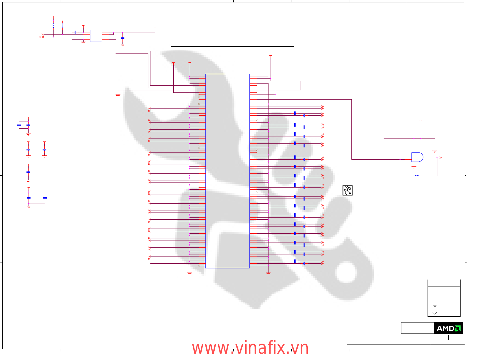
PART 1 OF 10
PART 1 OF 10
PCI-EXPRESS INTERFACE
PCI-EXPRESS INTERFACE
PCIE_TX0P
PCIE_TX0N
PCIE_TX1P
PCIE_TX1N
PCIE_TX2P
PCIE_TX2N
PCIE_TX3P
PCIE_TX3N
PCIE_TX4P
PCIE_TX4N
PCIE_TX5P
PCIE_TX5N
PCIE_TX6P
PCIE_TX6N
PCIE_TX7P
PCIE_TX7N
PCIE_TX8P
PCIE_TX8N
PCIE_TX9P
PCIE_TX9N
PCIE_TX10P
PCIE_TX10N
PCIE_TX11P
PCIE_TX11N
PCIE_TX12P
PCIE_TX12N
PCIE_TX13P
PCIE_TX13N
PCIE_TX14P
PCIE_TX14N
PCIE_TX15P
PCIE_TX15N
PCIE_CALRN
PCIE_CALRP
3
AH30
AG31
AG29
AF28
AF27
AF26
AD27
AD26
AC25
AB25
Y23
Y24
AB27
AB26
Y27
Y26
W24
W23
V27
U26
U24
U23
T26
T27
T24
T23
P27
P26
P24
P23
M27
N26
+1.1V
AA22
Y22
PCIE_CALRN
PCIE_CALRP
402
R82.0K R82.0K
402
R91.27K R91.27K
2
GFXTp0_PERp0 (1)
GFXTn0_PERn0 (1)
GFXTp1_PERp1 (1)
GFXTn1_PERn1 (1)
GFXTp2_PERp2 (1)
GFXTn2_PERn2 (1)
GFXTp3_PERp3 (1)
GFXTn3_PERn3 (1)
GFXTp4_PERp4 (1)
GFXTn4_PERn4 (1)
GFXTp5_PERp5 (1)
GFXTn5_PERn5 (1)
GFXTp6_PERp6 (1)
GFXTn6_PERn6 (1)
GFXTp7_PERp7 (1)
GFXTn7_PERn7 (1)
GFXTp8_PERp8 (1)
GFXTn8_PERn8 (1)
GFXTp9_PERp9 (1)
GFXTn9_PERn9 (1)
GFXTp10_PERp10 (1)
GFXTn10_PERn10 (1)
GFXTp11_PERp11 (1)
GFXTn11_PERn11 (1)
GFXTp12_PERp12 (1)
GFXTn12_PERn12 (1)
GFXTp13_PERp13 (1)
GFXTn13_PERn13 (1)
GFXTp14_PERp14 (1)
GFXTn14_PERn14 (1)
GFXTp15_PERp15 (1)
GFXTn15_PERn15 (1)
1
PERST#_buf(1)
A A
5
4
AL27
PERSTB
RV710_03_20_FINAL1
RV710_03_20_FINAL1
www.vinafix.vn
3
CONFIDENTIAL & PROPRIETARY TO ADVANCED MICRO DEVICES INC.
CONFIDENTIAL & PROPRIETARY TO ADVANCED MICRO DEVICES INC.
CONFIDENTIAL & PROPRIETARY TO ADVANCED MICRO DEVICES INC.
?2007 Advanced Micro Devices
?2007 Advanced Micro Devices
?2007 Advanced Micro Devices
This AMD Board schematic and design is the exclusive property of AMD,
This AMD Board schematic and design is the exclusive property of AMD,
This AMD Board schematic and design is the exclusive property of AMD,
and is provided only to entities under a non-disclosure agreement
and is provided only to entities under a non-disclosure agreement
and is provided only to entities under a non-disclosure agreement
with AMD for evaluation purposes. Further distribution or disclosure
with AMD for evaluation purposes. Further distribution or disclosure
with AMD for evaluation purposes. Further distribution or disclosure
is strictly prohibited. Use of this schematic and design for any purpose
is strictly prohibited. Use of this schematic and design for any purpose
is strictly prohibited. Use of this schematic and design for any purpose
other than evaluation requires a Board Technology License Agreement
other than evaluation requires a Board Technology License Agreement
other than evaluation requires a Board Technology License Agreement
with AMD. AMD makes no representations or warranties of any kind
with AMD. AMD makes no representations or warranties of any kind
with AMD. AMD makes no representations or warranties of any kind
regarding this schematic and design, including, not limited to,
regarding this schematic and design, including, not limited to,
regarding this schematic and design, including, not limited to,
any implied warranty of merchantibility or fitness for a particular
any implied warranty of merchantibility or fitness for a particular
any implied warranty of merchantibility or fitness for a particular
purpose, and disclaims responsibility forany consequences resulting
purpose, and disclaims responsibility forany consequences resulting
purpose, and disclaims responsibility forany consequences resulting
from use of the information included herein.
from use of the information included herein.
from use of the information included herein.
Title
Title
Title
RH LP RV710 DDR2 VGA (header) TVO DVI
RH LP RV710 DDR2 VGA (header) TVO DVI
2
RH LP RV710 DDR2 VGA (header) TVO DVI
Advanced Micro Devices Inc.
Advanced Micro Devices Inc.
Advanced Micro Devices Inc.
1 Commerce Valley Drive East
1 Commerce Valley Drive East
1 Commerce Valley Drive East
Markham, Ontario
Markham, Ontario
Markham, Ontario
Thursday, October 23, 2008
Thursday, October 23, 2008
Thursday, October 23, 2008
Sheet
Sheet
Sheet
of
222
of
222
of
222
1
Doc No.
Doc No.
Doc No.
105-B750XX-00A
105-B750XX-00A
105-B750XX-00A
RevDate:
RevDate:
RevDate:
0
0
0
Page 3
5
D D
GPIO_0(10)
GPIO_1(10)
GPIO_2(10)
GPIO_3(1)
C C
GPIO_4(1)
GPIO_5(10)
GPIO_7(10)
GPIO_8
GPIO_8(10)
GPIO_9
GPIO_11(10)
GPIO_12(10)
GPIO_13(10)
R13 33RR13 33R
GPIO_9 GPIO9_SI
R14 33RR14 33R
GPIO_10
R15 33RR15 33R
GPIO_16(10)
GPIO_22
R16 33RR16 33R
R621KR62
1K
GPIO_0
GPIO_1
GPIO_2
GPIO_3
GPIO_4
GPIO_5
GPIO_7
GPIO8_SO
GPIO10_SCK
GPIO_11
GPIO_12
GPIO_13
GPIO_16
GPIO_22_CS
JTAG_TRSTB
HPD4(16)
B B
HPD1(18)
+1.8V
R21 221RR21 221R
R22 110RR22 110R
C53 100nFC53 100nF
R351KR35
A A
4
U1B
VREFG
U1B
U1
DVPCLK
AC7
DVPCNTL_0
Y2
DVPCNTL_1
U5
DVPCNTL_2
AA1
DVPCNTL_MVP_0
Y4
DVPCNTL_MVP_1
Y7
DVPDATA_0
V2
DVPDATA_1
Y8
DVPDATA_2
V4
DVPDATA_3
AB7
DVPDATA_4
W1
DVPDATA_5
AB8
DVPDATA_6
W3
DVPDATA_7
AB9
DVPDATA_8
W5
DVPDATA_9
AC6
DVPDATA_10
W6
DVPDATA_11
AD7
DVPDATA_12
AA3
DVPDATA_13
AC8
DVPDATA_14
AA5
DVPDATA_15
AE8
DVPDATA_16
AA6
DVPDATA_17
AE9
DVPDATA_18
AB4
DVPDATA_19
AD9
DVPDATA_20
AB2
DVPDATA_21
AC10
DVPDATA_22
AC5
DVPDATA_23
U6
GPIO_0
U10
GPIO_1
T10
GPIO_2
U8
GPIO_3_SMBDATA
U7
GPIO_4_SMBCLK
T9
GPIO_5_AC_BATT
T8
GPIO_6_TACH
T7
GPIO_7_BLON
P10
GPIO_8_ROMSO
P4
GPIO_9_ROMSI
P2
GPIO_10_ROMSCK
N6
GPIO_11
N5
GPIO_12
N3
GPIO_13
Y9
GPIO_14_HPD2
N1
GPIO_15_PWRCNTL_0
M4
GPIO_16_SSIN
R6
GPIO_17_THERMAL_INT
W10
GPIO_18_HPD3
M2
GPIO_19_CTF
P8
GPIO_20_PWRCNTL_1
P7
GPIO_21_BB_EN
N8
GPIO_22_ROMCSB
N7
GPIO_23_CLKREQB
L6
JTAG_TRSTB
L5
JTAG_TDI
L3
JTAG_TCK
L1
JTAG_TMS
K4
JTAG_TDO
AB13
GENERICA
W8
GENERICB
W9
GENERICC
W7
GENERICD
AD10
GENERICE_HPD4
AC14
HPD1
AC16
VREFG
N10
NC_PWRGOOD
AB22
RSVD#8
AC22
RSVD#9
L9
NC#1
N9
NC#2
AB16
RSVD#3
AB12
RSVD#2
AB11
RSVD#1
AF24
TESTEN
RV710_03_20_FINAL1
RV710_03_20_FINAL1
PART 2 OF 10
PART 2 OF 10
DVP PORT DAC1
DVP PORT DAC1
I/O
I/O
RESERVED
RESERVED
DAC2
DAC2
HSYNC
VSYNC
AVDD
AVSSQ
VDD1DI
VSS1DI
RSET
H2SYNC
V2SYNC
COMP
A2VDD
A2VDDQ
A2VSSQ
VDD2DI
VSS2DI
R2SET
AM26
R
AK26
RB
AL25
G
AJ25
GB
AH24
B
AG25
BB
AH26
AJ27
AG24
AE22
AE23
AD23
RSET
AD22
AM12
R2
AK12
R2B
AL11
G2
AJ11
G2B
AK10
B2
AL9
B2B
AL13
AJ13
AH12
C
AM10
Y
AJ9
+A2VDD
AE20
+A2VDDQ
AE17
AE19
+VDD2DI
AD19
AC19
R2SET
AG13
1K
+AVDD
+VDD1DI
R12 499RR12 499R
R23 715RR23 715R
3
A_R_DAC1 (16)
A_RB_DAC1 (16)
A_G_DAC1 (16)
A_GB_DAC1 (16)
A_B_DAC1 (16)
A_BB_DAC1 (16)
A_HSYNC_DAC1 (10,16)
A_VSYNC_DAC1 (10,16)
C1051
C1051
C1050
C1050
100nF
100nF
10nF
10nF
10V X5R
10V X7R
402
402 10%
10%
C1053
C1053
C1054
C1054
100nF
100nF
10nF
10nF
10V
X7R 10V X5R
402 10%
402 10%
Place very close to ASIC balls.
A_R_DAC2 (17)
A_RB_DAC2 (17)
A_G_DAC2 (17)
A_GB_DAC2 (17)
A_B_DAC2 (17)
A_BB_DAC2 (17)
A_HSYNC_DAC2 (17)
A_VSYNC_DAC2 (17)
C2052
C2052
100nF
100nF
C2054
C2054
10nF
10nF
Place very close to ASIC balls.
C1052
C1052
1uF_6.3V
1uF_6.3V
6.3V
402 10%
C1055
C1055
1uF_6.3V
1uF_6.3V
6.3V X5R
402 10%
C2058
C2058
10nF
10nF
X5R
C2051
C2051
100nF
100nF
C2053
C2053
1uF_6.3V
1uF_6.3V
C2055
C2055
100nF
100nF
B1 BLM15BD121SN1B1 BLM15BD121SN1
C1056
C1056
4.7uF_6.3V
4.7uF_6.3V
B2 BLM15BD121SN1B2 BLM15BD121SN1
C2050
C2050
1uF_6.3V
1uF_6.3V
C2056
C2056
1uF_6.3V
1uF_6.3V
B3 120R_300mAB3 120R_300mA
C2057
C2057
4.7uF_6.3V
4.7uF_6.3V
B4
B4
BLM15BD121SN1
BLM15BD121SN1
B5
B5
BLM15BD121SN1
BLM15BD121SN1
2
+1.8V
+3.3V
+1.8V
+1.8V
GPIO_22
GPIO_8
+3.3V
ROM_WP
+3.3V
R24
R24
10K
10K
U2
U2
1
CE#
2
SO
3
WP#
GND4SI
PM25LV512A-100SCE
PM25LV512A-100SCE
HOLD#
1
+3.3V
8
VCC
7
GPIO_10
6
SCK
GPIO_9
5
C57
C57
100nF
100nF
CONFIDENTIAL & PROPRIETARY TO ADVANCED MICRO DEVICES INC.
CONFIDENTIAL & PROPRIETARY TO ADVANCED MICRO DEVICES INC.
CONFIDENTIAL & PROPRIETARY TO ADVANCED MICRO DEVICES INC.
?2007 Advanced Micro Devices
?2007 Advanced Micro Devices
?2007 Advanced Micro Devices
This AMD Board schematic and design is the exclusive property of AMD,
This AMD Board schematic and design is the exclusive property of AMD,
This AMD Board schematic and design is the exclusive property of AMD,
and is provided only to entities under a non-disclosure agreement
and is provided only to entities under a non-disclosure agreement
and is provided only to entities under a non-disclosure agreement
with AMD for evaluation purposes. Further distribution or disclosure
with AMD for evaluation purposes. Further distribution or disclosure
with AMD for evaluation purposes. Further distribution or disclosure
is strictly prohibited. Use of this schematic and design for any purpose
is strictly prohibited. Use of this schematic and design for any purpose
is strictly prohibited. Use of this schematic and design for any purpose
other than evaluation requires a Board Technology License Agreement
other than evaluation requires a Board Technology License Agreement
other than evaluation requires a Board Technology License Agreement
with AMD. AMD makes no representations or warranties of any kind
with AMD. AMD makes no representations or warranties of any kind
with AMD. AMD makes no representations or warranties of any kind
regarding this schematic and design, including, not limited to,
regarding this schematic and design, including, not limited to,
regarding this schematic and design, including, not limited to,
any implied warranty of merchantibility or fitness for a particular
any implied warranty of merchantibility or fitness for a particular
any implied warranty of merchantibility or fitness for a particular
purpose, and disclaims responsibility forany consequences resulting
purpose, and disclaims responsibility forany consequences resulting
purpose, and disclaims responsibility forany consequences resulting
from use of the information included herein.
from use of the information included herein.
from use of the information included herein.
Title
Title
Title
RH LP RV710 DDR2 VGA (header) TVO DVI
RH LP RV710 DDR2 VGA (header) TVO DVI
5
4
www.vinafix.vn
3
2
RH LP RV710 DDR2 VGA (header) TVO DVI
Advanced Micro Devices Inc.
Advanced Micro Devices Inc.
Advanced Micro Devices Inc.
1 Commerce Valley Drive East
1 Commerce Valley Drive East
1 Commerce Valley Drive East
Markham, Ontario
Markham, Ontario
Markham, Ontario
Thursday, October 23, 2008
Thursday, October 23, 2008
Thursday, October 23, 2008
Sheet
Sheet
Sheet
of
322
of
322
of
322
1
Doc No.
Doc No.
Doc No.
105-B750XX-00A
105-B750XX-00A
105-B750XX-00A
RevDate:
RevDate:
RevDate:
0
0
0
Page 4
5
D D
NS6 NS_VIANS6 NS_VIA
1 2
+VDDC
B10
B10
BLM15BD121SN1
BLM15BD121SN1
RV710: Install B10, do not install B9
RV810: Install B9, do not install B10
C82
C82
12pF_50V
12pF_50V
C83
C83
12pF_50V
12pF_50V
C C
XTALIN_S
2 1
XTALOUT_S
Y2
Y2
27.000MHz_10PPM
27.000MHz_10PPM
4
C69
C69
1uF_6.3V
1uF_6.3V
XTALIN
XTALOUT
C70
C70
1uF_6.3V
1uF_6.3V
GND_SPVSS
C71
C71
100nF
100nF
R311MR31
1M
3
U1J
U1J
Part 10 of 10
Part 10 of 10
XTAL / PLL
XTAL / PLL
H7
NC_SPV18
GND_SPVSS
+SPV10
C72
C72
10nF
10nF
XTALIN
XTALOUT
J7
H8
AM28
AK28
SPVSS
SPV10
XTALIN
XTALOUT
RV710_03_20_FINAL1
RV710_03_20_FINAL1
DPLL_PVDD
DPLL_PVSS
DPLL_VDDC
PCIE_PVDD
NC_MPV18
AF14
AE14
AD14
AM30
L8
+DPLL_PVDD
+DPLL_VDDC
+PCIE_PVDD
GND_PVSS
C73
C73
1uF_6.3V
1uF_6.3V
2
C59
C59
10nF
10nF
GND_PVSS
C65
C65
10nF
10nF
C74
C74
10nF
10nF
C66
C66
100nF
100nF
100nF
100nF
C64
C64
100nF
100nF
10uF_X6S
10uF_X6S
C67
C67
1uF_6.3V
1uF_6.3V
MC89
MC89
C75
C75
4.7uF_6.3V
4.7uF_6.3V
Overlap Overlap
C88
C63
C63
Overlap
C68
C68
10uF_X6S
10uF_X6S
C88
10uF_X6S
10uF_X6S
B8
B8
BLM15BD121SN1
BLM15BD121SN1
B11
B11
BLM15BD121SN1
BLM15BD121SN1
1
B7
B7
BLM15BD121SN1
BLM15BD121SN1
+1.1V
+1.8V
+1.8V
NS5NS_VIA NS5NS_VIA
12
+3.3V
R36
R36
4.7K
DDC6 BUS:
I2C Address Function Device
B B
A A
5
0x90 DS4402I2C VDDC Control
0x98 LM63 - External
SCL / SDA BUS:
I2C Address Function Device
N/A N/A N/A
Temperature Sensor
LM63
+1.8V
4
B4002
B4002
BLM15BD121SN1
BLM15BD121SN1
DDC6CLK
DDC6DATA
C4020
C4020
1uF_6.3V
1uF_6.3V
4.7K
+3.3V
R33
R33
4.7K
4.7K
SCL
SDA
+TSVDD
C4021
C4021
100nF
100nF
GND
www.vinafix.vn
R37
R37
4.7K
4.7K
R34
R34
4.7K
4.7K
U1H
U1H
AC1
DDC6CLK
AC3
DDC6DATA
R1
SCL
R3
SDA
RV710_03_20_FINAL1
RV710_03_20_FINAL1
AD17
AC17
U1I
U1I
TSVDD
TSVSS
RV710_03_20_FINAL1
RV710_03_20_FINAL1
Part 8 of 10
Part 8 of 10
I2C / DDC / AUX
I2C / DDC / AUX
TMDP / DAC1LVTMDP / DAC2
TMDP / DAC1LVTMDP / DAC2
DDCCLK_AUX5P
DDCDATA_AUX5N
NC_DDCCLK_AUX7P
NC_DDCDATA_AUX7N
Part 9 of 10
Part 9 of 10
TSS FDO
TSS FDO
3
TS_FDO
DMINUS
DDC1DATA
DDC2DATA
DPLUS
AUX1P
AUX1N
DDC1CLK
AUX2P
AUX2N
DDC2CLK
AD2
AD4
AE6
AE5
AD13
AD11
AC11
AC13
AE16
AD16
AD20
AC20
TS_FDO
R5
T4
T2
DDC1CLK (17)
DDC1DATA (17)
DDC2CLK (18)
DDC2DATA (18)
DDCAUX5P (16)
DDCAUX5N (16)
TS_FDO (19)
CONFIDENTIAL & PROPRIETARY TO ADVANCED MICRO DEVICES INC.
CONFIDENTIAL & PROPRIETARY TO ADVANCED MICRO DEVICES INC.
CONFIDENTIAL & PROPRIETARY TO ADVANCED MICRO DEVICES INC.
?2007 Advanced Micro Devices
?2007 Advanced Micro Devices
?2007 Advanced Micro Devices
This AMD Board schematic and design is the exclusive property of AMD,
This AMD Board schematic and design is the exclusive property of AMD,
This AMD Board schematic and design is the exclusive property of AMD,
and is provided only to entities under a non-disclosure agreement
and is provided only to entities under a non-disclosure agreement
and is provided only to entities under a non-disclosure agreement
with AMD for evaluation purposes. Further distribution or disclosure
with AMD for evaluation purposes. Further distribution or disclosure
with AMD for evaluation purposes. Further distribution or disclosure
is strictly prohibited. Use of this schematic and design for any purpose
is strictly prohibited. Use of this schematic and design for any purpose
is strictly prohibited. Use of this schematic and design for any purpose
other than evaluation requires a Board Technology License Agreement
other than evaluation requires a Board Technology License Agreement
other than evaluation requires a Board Technology License Agreement
with AMD. AMD makes no representations or warranties of any kind
with AMD. AMD makes no representations or warranties of any kind
with AMD. AMD makes no representations or warranties of any kind
regarding this schematic and design, including, not limited to,
regarding this schematic and design, including, not limited to,
regarding this schematic and design, including, not limited to,
any implied warranty of merchantibility or fitness for a particular
any implied warranty of merchantibility or fitness for a particular
any implied warranty of merchantibility or fitness for a particular
purpose, and disclaims responsibility forany consequences resulting
purpose, and disclaims responsibility forany consequences resulting
purpose, and disclaims responsibility forany consequences resulting
from use of the information included herein.
from use of the information included herein.
from use of the information included herein.
Title
Title
Title
RH LP RV710 DDR2 VGA (header) TVO DVI
RH LP RV710 DDR2 VGA (header) TVO DVI
2
RH LP RV710 DDR2 VGA (header) TVO DVI
Advanced Micro Devices Inc.
Advanced Micro Devices Inc.
Advanced Micro Devices Inc.
1 Commerce Valley Drive East
1 Commerce Valley Drive East
1 Commerce Valley Drive East
Markham, Ontario
Markham, Ontario
Markham, Ontario
Thursday, October 23, 2008
Thursday, October 23, 2008
Thursday, October 23, 2008
Sheet
Sheet
Sheet
of
422
of
422
of
422
1
Doc No.
Doc No.
Doc No.
105-B750XX-00A
105-B750XX-00A
105-B750XX-00A
RevDate:
RevDate:
RevDate:
0
0
0
Page 5
5
4
3
2
1
TMDP INTERFACE
U1F
AG8
AG7
AF11
AE11
AF6
AF7
AG10
AG11
AE13
AF13
U1F
DPA_PVDD
DPA_PVSS
NC_DPA_VDD18#2
NC_DPA_VDD18#1
DPA_VDD10#1
DPA_VDD10#2
DPB_PVDD
DPB_PVSS
NC_DPB_VDD18#1
NC_DPB_VDD18#2
D D
C C
+1.8V
+1.8V
+1.1V
B2505
B2505
BLM15BD121SN1
BLM15BD121SN1
B2503
B2503
30R_1A
30R_1A
B2504
B2504
BLM15BD121SN1
BLM15BD121SN1
4.7uF_6.3V
4.7uF_6.3V
C2513
C2513
4.7uF_6.3V
4.7uF_6.3V
C2516
C2516
4.7uF_6.3V
4.7uF_6.3V
C2510
C2510
1uF_6.3V
1uF_6.3V
1uF_6.3V
1uF_6.3V
C2517
C2517
1uF_6.3V
1uF_6.3V
C2511
C2511
C2509
C2509
C2515
C2515
100nF
100nF
C2514
C2514
100nF
100nF
C2512
C2512
100nF
100nF
+DPA_PVDD
+DPA_VDD10
+DPB_PVDD
PART 6 OF 10
PART 6 OF 10
DPA
DPA
DPB
DPB
TX2P_DPA0P
TX2M_DPA0N
TX1P_DPA1P
TX1M_DPA1N
TX0P_DPA2P
TX0M_DPA2N
TXCAP_DPA3P
TXCAM_DPA3N
DPA_VSSR#5
DPA_VSSR#3
DPA_VSSR#4
DPA_VSSR#2
DPA_VSSR#1
TX5P_DPB0P
TX5M_DPB0N
TX4P_DPB1P
TX4M_DPB1N
TX3P_DPB2P
TX3M_DPB2N
TXCBP_DPB3P
TXCBM_DPB3N
DPB_VSSR#5
DPB_VSSR#2
DPB_VSSR#1
DPB_VSSR#4
DPB_VSSR#3
AK3
AK1
AH3
AH1
AG3
AG5
AF2
AF4
AH5
AG1
AG6
AE3
AE1
AK8
AL7
AJ7
AH6
AK6
AM5
AK5
AM3
AM8
AG9
AF10
AM6
AH8
TX2P (18)
TX2M (18)
TX1P (18)
TX1M (18)
TX0P (18)
TX0M (18)
TXCAP (18)
TXCAM (18)
CALIBRATION
+1.1V
C2519
C2519
100nF
100nF
+DPB_VDD10
B2506
B B
A A
5
B2506
30R_1A
30R_1A
C2518
C2518
4.7uF_6.3V
4.7uF_6.3V
C2520
C2520
1uF_6.3V
1uF_6.3V
4
AF8
DPB_VDD10#1
AF9
DPB_VDD10#2
RV710_03_20_FINAL1
RV710_03_20_FINAL1
CALIBRATION
3
DPAB_CALR
AE10
DPAB_CALR
CONFIDENTIAL & PROPRIETARY TO ADVANCED MICRO DEVICES INC.
CONFIDENTIAL & PROPRIETARY TO ADVANCED MICRO DEVICES INC.
CONFIDENTIAL & PROPRIETARY TO ADVANCED MICRO DEVICES INC.
?2007 Advanced Micro Devices
?2007 Advanced Micro Devices
?2007 Advanced Micro Devices
This AMD Board schematic and design is the exclusive property of AMD,
This AMD Board schematic and design is the exclusive property of AMD,
This AMD Board schematic and design is the exclusive property of AMD,
and is provided only to entities under a non-disclosure agreement
and is provided only to entities under a non-disclosure agreement
and is provided only to entities under a non-disclosure agreement
with AMD for evaluation purposes. Further distribution or disclosure
with AMD for evaluation purposes. Further distribution or disclosure
with AMD for evaluation purposes. Further distribution or disclosure
is strictly prohibited. Use of this schematic and design for any purpose
is strictly prohibited. Use of this schematic and design for any purpose
is strictly prohibited. Use of this schematic and design for any purpose
other than evaluation requires a Board Technology License Agreement
other than evaluation requires a Board Technology License Agreement
other than evaluation requires a Board Technology License Agreement
with AMD. AMD makes no representations or warranties of any kind
with AMD. AMD makes no representations or warranties of any kind
with AMD. AMD makes no representations or warranties of any kind
regarding this schematic and design, including, not limited to,
regarding this schematic and design, including, not limited to,
regarding this schematic and design, including, not limited to,
any implied warranty of merchantibility or fitness for a particular
any implied warranty of merchantibility or fitness for a particular
any implied warranty of merchantibility or fitness for a particular
purpose, and disclaims responsibility forany consequences resulting
purpose, and disclaims responsibility forany consequences resulting
purpose, and disclaims responsibility forany consequences resulting
from use of the information included herein.
from use of the information included herein.
from use of the information included herein.
Title
Title
Title
RH LP RV710 DDR2 VGA (header) TVO DVI
RH LP RV710 DDR2 VGA (header) TVO DVI
RH LP RV710 DDR2 VGA (header) TVO DVI
2
R2500150R R2500150R
1%
Advanced Micro Devices Inc.
Advanced Micro Devices Inc.
Advanced Micro Devices Inc.
1 Commerce Valley Drive East
1 Commerce Valley Drive East
1 Commerce Valley Drive East
Markham, Ontario
Markham, Ontario
Markham, Ontario
Thursday, October 23, 2008
Thursday, October 23, 2008
Thursday, October 23, 2008
Sheet
Sheet
Sheet
of
522
of
522
of
522
Doc No.
Doc No.
Doc No.
105-B750XX-00A
105-B750XX-00A
105-B750XX-00A
1
RevDate:
RevDate:
RevDate:
0
0
0
www.vinafix.vn
Page 6
5
4
3
2
1
LVTMDP INTERFACE
D D
C C
+1.8V
1uF_6.3V
1uF_6.3V
1uF_6.3V
1uF_6.3V
C1507
C1507
1uF_6.3V
1uF_6.3V
C1501
C1501
C1504
C1504
+DPE_PVDD
C1509
C1509
1uF_6.3V
1uF_6.3V
+DPE_VDD18
C1510
C1510
1uF_6.3V
1uF_6.3V
+DPE_VDD10
C1511
C1511
1uF_6.3V
1uF_6.3V
C1502
C1502
100nF
100nF
C1505
C1505
100nF
100nF
C1508
C1508
100nF
100nF
B1500
B1500
BLM15BD121SN1
BLM15BD121SN1
+1.8V
B1501
B1501
BLM15BD121SN1
BLM15BD121SN1
B B
+1.1V
C1500
C1500
4.7uF_6.3V
4.7uF_6.3V
C1503
C1503
4.7uF_6.3V
4.7uF_6.3V
C1506
C1506
4.7uF_6.3V
4.7uF_6.3V
U1G
U1G
AG19
NC_DPF_PVDD
AF20
NC_DPF_PVSS
AG17
DPF_VDD18#2
AF16
DPF_VDD18#1
AG22
DPF_VDD10#2
AF22
DPF_VDD10#1
AG18
DPE_PVDD
AF19
DPE_PVSS
AG16
DPE_VDD18#2
AG15
DPE_VDD18#1
AG21
DPE_VDD10#2
AG20
DPE_VDD10#1
RV710_03_20_FINAL1
RV710_03_20_FINAL1
Part 7 of 10
Part 7 of 10
DPF
DPF
DPE
DPE
CALIBRATION
CALIBRATION
RSVD#6
RSVD#4
T2X5P_DPF0P
T2X5M_DPF0N
T2X4P_DPF1P
T2X4M_DPF1N
T2X3P_DPF2P
T2X3M_DPF2N
T2XCFP_DPF3P
T2XCFM_DPF3N
DPF_VSSR#4
DPF_VSSR#5
DPF_VSSR#2
DPF_VSSR#1
DPF_VSSR#3
RSVD#7
RSVD#5
T2X2P_DPE0P
T2X2M_DPE0N
T2X1P_DPE1P
T2X1M_DPE1N
T2X0P_DPE2P
T2X0M_DPE2N
T2XCEP_DPE3P
T2XCEM_DPE3N
DPE_VSSR#3
DPE_VSSR#2
DPE_VSSR#1
DPE_VSSR#4
DPE_VSSR#5
DPEF_CALR
AK24
AJ23
AL23
AK22
AH22
AJ21
AL21
AK20
AH20
AJ19
AM22
AM24
AG23
AF23
AM20
AL19
AK18
AH18
AJ17
AL17
AK16
AH16
AJ15
AL15
AK14
AM14
AH14
AG14
AM16
AM18
AF17
DPEF_CALR
T2X5P (16)
T2X5M (16)
T2X4P (16)
T2X4M (16)
T2X3P (16)
T2X3M (16)
T2X2P (16)
T2X2M (16)
T2X1P (16)
T2X1M (16)
T2X0P (16)
T2X0M (16)
T2XCEP (16)
T2XCEM (16)
1%
R1500150R R1500150RB1502 30R_1AB1502 30R_1A
A A
5
4
3
CONFIDENTIAL & PROPRIETARY TO ADVANCED MICRO DEVICES INC.
CONFIDENTIAL & PROPRIETARY TO ADVANCED MICRO DEVICES INC.
CONFIDENTIAL & PROPRIETARY TO ADVANCED MICRO DEVICES INC.
?2007 Advanced Micro Devices
?2007 Advanced Micro Devices
?2007 Advanced Micro Devices
This AMD Board schematic and design is the exclusive property of AMD,
This AMD Board schematic and design is the exclusive property of AMD,
This AMD Board schematic and design is the exclusive property of AMD,
and is provided only to entities under a non-disclosure agreement
and is provided only to entities under a non-disclosure agreement
and is provided only to entities under a non-disclosure agreement
with AMD for evaluation purposes. Further distribution or disclosure
with AMD for evaluation purposes. Further distribution or disclosure
with AMD for evaluation purposes. Further distribution or disclosure
is strictly prohibited. Use of this schematic and design for any purpose
is strictly prohibited. Use of this schematic and design for any purpose
is strictly prohibited. Use of this schematic and design for any purpose
other than evaluation requires a Board Technology License Agreement
other than evaluation requires a Board Technology License Agreement
other than evaluation requires a Board Technology License Agreement
with AMD. AMD makes no representations or warranties of any kind
with AMD. AMD makes no representations or warranties of any kind
with AMD. AMD makes no representations or warranties of any kind
regarding this schematic and design, including, not limited to,
regarding this schematic and design, including, not limited to,
regarding this schematic and design, including, not limited to,
any implied warranty of merchantibility or fitness for a particular
any implied warranty of merchantibility or fitness for a particular
any implied warranty of merchantibility or fitness for a particular
purpose, and disclaims responsibility forany consequences resulting
purpose, and disclaims responsibility forany consequences resulting
purpose, and disclaims responsibility forany consequences resulting
from use of the information included herein.
from use of the information included herein.
from use of the information included herein.
Title
Title
Title
RH LP RV710 DDR2 VGA (header) TVO DVI
RH LP RV710 DDR2 VGA (header) TVO DVI
RH LP RV710 DDR2 VGA (header) TVO DVI
2
Advanced Micro Devices Inc.
Advanced Micro Devices Inc.
Advanced Micro Devices Inc.
1 Commerce Valley Drive East
1 Commerce Valley Drive East
1 Commerce Valley Drive East
Markham, Ontario
Markham, Ontario
Markham, Ontario
Thursday, October 23, 2008
Thursday, October 23, 2008
Thursday, October 23, 2008
Sheet
Sheet
Sheet
of
622
of
622
of
622
Doc No.
Doc No.
Doc No.
105-B750XX-00A
105-B750XX-00A
105-B750XX-00A
1
RevDate:
RevDate:
RevDate:
0
0
0
www.vinafix.vn
Page 7
5
4
3
2
1
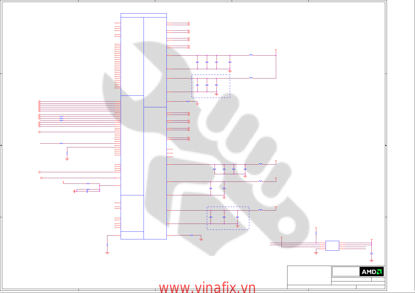
MEMORY INTERFACE
M_MDA[63..0](15)
U1C
U1C
D D
C C
B B
Stitching caps.
Place where memory transitions between L1 and L4.
+MVDD
C201
C201
C200
C200
100nF
100nF
100nF
100nF
C206
C206
C205
C205
100nF
100nF
100nF
100nF
+MVDD
R291
R291
100R
100R
R292
R292
100R
100R
+MVDD
R293
R293
100R
100R
MVREFS_A
R294
R294
100R
100R
C202
C202
100nF
100nF
C207
C207
100nF
100nF
MVREFD_A
C297
C297
100nF
100nF
C203
C203
100nF
100nF
C208
C208
100nF
100nF
C295
C295
100nF
100nF
C298
C298
10nF
10nF
C204
C204
100nF
100nF
C209
C209
100nF
100nF
C296
C296
10nF
10nF
MEMTEST
R298
R298
243R
243R
M_MDA0
M_MDA1
M_MDA2
M_MDA3
M_MDA4
M_MDA5
M_MDA6
M_MDA7
M_MDA8
M_MDA9
M_MDA10
M_MDA11
M_MDA12
M_MDA13
M_MDA14
M_MDA15
M_MDA16
M_MDA17
M_MDA18
M_MDA19
M_MDA20
M_MDA21
M_MDA22
M_MDA23
M_MDA24
M_MDA25
M_MDA26
M_MDA27
M_MDA28
M_MDA29
M_MDA30
M_MDA31
M_MDA32
M_MDA33
M_MDA34
M_MDA35
M_MDA36
M_MDA37
M_MDA38
M_MDA39
M_MDA40
M_MDA41
M_MDA42
M_MDA43
M_MDA44
M_MDA45
M_MDA46
M_MDA47
M_MDA48
M_MDA49
M_MDA50
M_MDA51
M_MDA52
M_MDA53
M_MDA54
M_MDA55
M_MDA56
M_MDA57
M_MDA58
M_MDA59
M_MDA60
M_MDA61
M_MDA62
M_MDA63
K27
J29
H30
H32
G29
F28
F32
F30
C30
F27
A28
C28
E27
G26
D26
F25
A25
C25
E25
D24
E23
F23
D22
F21
E21
D20
F19
A19
D18
F17
A17
C17
E17
D16
F15
A15
D14
F13
A13
C13
E11
A11
C11
F11
A9
C9
F9
D8
E7
A7
C7
F7
A5
E5
C3
E1
G7
G6
G1
G3
J6
J1
J3
J5
K26
J26
K8
L7
J8
G20
G14
K7
K25
J25
RV710_03_20_FINAL1
RV710_03_20_FINAL1
DQA_0
DQA_1
DQA_2
DQA_3
DQA_4
DQA_5
DQA_6
DQA_7
DQA_8
DQA_9
DQA_10
DQA_11
DQA_12
DQA_13
DQA_14
DQA_15
DQA_16
DQA_17
DQA_18
DQA_19
DQA_20
DQA_21
DQA_22
DQA_23
DQA_24
DQA_25
DQA_26
DQA_27
DQA_28
DQA_29
DQA_30
DQA_31
DQA_32
DQA_33
DQA_34
DQA_35
DQA_36
DQA_37
DQA_38
DQA_39
DQA_40
DQA_41
DQA_42
DQA_43
DQA_44
DQA_45
DQA_46
DQA_47
DQA_48
DQA_49
DQA_50
DQA_51
DQA_52
DQA_53
DQA_54
DQA_55
DQA_56
DQA_57
DQA_58
DQA_59
DQA_60
DQA_61
DQA_62
DQA_63
MVREFDA
MVREFSA
CLKTESTA
CLKTESTB
MEM_CALRP1
NC_MAA_13
NC_MAA_14
NC_MEM_CALRN1
NC_MEM_CALRP0
NC_MEM_CALRN0
PART 3 OF 10
PART 3 OF 10
MEMORY
MEMORY
INTERFACE
INTERFACE
READ STROBE
READ STROBE
WRITE STROBE
WRITE STROBE
MAA_0
MAA_1
MAA_2
MAA_3
MAA_4
MAA_5
MAA_6
MAA_7
MAA_8
MAA_9
MAA_10
MAA_11
MAA_BA0
MAA_BA1
MAA_12
MAA_BA2
DQMA_0
DQMA_1
DQMA_2
DQMA_3
DQMA_4
DQMA_5
DQMA_6
DQMA_7
QSA_0
QSA_1
QSA_2
QSA_3
QSA_4
QSA_5
QSA_6
QSA_7
QSA_0B
QSA_1B
QSA_2B
QSA_3B
QSA_4B
QSA_5B
QSA_6B
QSA_7B
ODTA0
ODTA1
CLKA0
CLKA1
CLKA0B
CLKA1B
RASA0B
RASA1B
CASA0B
CASA1B
CSA0B_0
CSA0B_1
CSA1B_0
CSA1B_1
CKEA0
CKEA1
WEA0B
WEA1B
DRAM_RST
M_MAA0
K17
M_MAA1
J20
M_MAA2
H23
M_MAA3
G23
M_MAA4
G24
M_MAA5
H24
M_MAA6
J19
M_MAA7
K19
M_MAA8
J14
M_MAA9
K14
M_MAA10
J11
M_MAA11
J13
J16
BA0 (15)
L15
BA1 (15)
M_MAA12
H11
G11
BA2 (15)
M_DQMA#0
E32
M_DQMA#1
E30
M_DQMA#2
A21
M_DQMA#3
C21
M_DQMA#4
E13
M_DQMA#5
D12
M_DQMA#6
E3
M_DQMA#7
F4
M_QSA0
H28
M_QSA1
C27
M_QSA2
A23
M_QSA3
E19
M_QSA4
E15
M_QSA5
D10
M_QSA6
D6
M_QSA7
G5
H27
A27
C23
C19
C15
E9
C5
H4
L18
K16
H26
G9
H25
H9
G22
G17
G19
G16
H22
J22
G13
K13
K20
J17
G25
H10
L10
ODTA0 (15)
ODTA1 (15)
CLKA0 (15)
CLKA1 (15)
CLKA#0 (15)
CLKA#1 (15)
RASA#0 (15)
RASA#1 (15)
CASA#0 (15)
CASA#1 (15)
CSA#0_0 (15)
CSA#1_0 (15)
CKEA0 (15)
CKEA1 (15)
WEA#0 (15)
WEA#1 (15)
M_MAA[12..0] (15)
M_DQMA#[7..0] (15)
M_QSA[7..0] (15)
MR295
MR295
4.7K
4.7K
A A
5
DIVIDER RESISTORS DDR2
MVREF TO 1.8V
MVREF TO GND
100R
100R
CONFIDENTIAL & PROPRIETARY TO ADVANCED MICRO DEVICES INC.
CONFIDENTIAL & PROPRIETARY TO ADVANCED MICRO DEVICES INC.
CONFIDENTIAL & PROPRIETARY TO ADVANCED MICRO DEVICES INC.
?2007 Advanced Micro Devices
?2007 Advanced Micro Devices
?2007 Advanced Micro Devices
This AMD Board schematic and design is the exclusive property of AMD,
This AMD Board schematic and design is the exclusive property of AMD,
This AMD Board schematic and design is the exclusive property of AMD,
and is provided only to entities under a non-disclosure agreement
and is provided only to entities under a non-disclosure agreement
and is provided only to entities under a non-disclosure agreement
with AMD for evaluation purposes. Further distribution or disclosure
with AMD for evaluation purposes. Further distribution or disclosure
with AMD for evaluation purposes. Further distribution or disclosure
is strictly prohibited. Use of this schematic and design for any purpose
is strictly prohibited. Use of this schematic and design for any purpose
is strictly prohibited. Use of this schematic and design for any purpose
other than evaluation requires a Board Technology License Agreement
other than evaluation requires a Board Technology License Agreement
other than evaluation requires a Board Technology License Agreement
with AMD. AMD makes no representations or warranties of any kind
with AMD. AMD makes no representations or warranties of any kind
with AMD. AMD makes no representations or warranties of any kind
regarding this schematic and design, including, not limited to,
regarding this schematic and design, including, not limited to,
regarding this schematic and design, including, not limited to,
any implied warranty of merchantibility or fitness for a particular
any implied warranty of merchantibility or fitness for a particular
any implied warranty of merchantibility or fitness for a particular
purpose, and disclaims responsibility forany consequences resulting
purpose, and disclaims responsibility forany consequences resulting
purpose, and disclaims responsibility forany consequences resulting
from use of the information included herein.
from use of the information included herein.
from use of the information included herein.
Title
Title
Title
RH LP RV710 DDR2 VGA (header) TVO DVI
RH LP RV710 DDR2 VGA (header) TVO DVI
4
www.vinafix.vn
3
2
RH LP RV710 DDR2 VGA (header) TVO DVI
Advanced Micro Devices Inc.
Advanced Micro Devices Inc.
Advanced Micro Devices Inc.
1 Commerce Valley Drive East
1 Commerce Valley Drive East
1 Commerce Valley Drive East
Markham, Ontario
Markham, Ontario
Markham, Ontario
Thursday, October 23, 2008
Thursday, October 23, 2008
Thursday, October 23, 2008
Sheet
Sheet
Sheet
of
722
of
722
of
722
1
Doc No.
Doc No.
Doc No.
105-B750XX-00A
105-B750XX-00A
105-B750XX-00A
RevDate:
RevDate:
RevDate:
0
0
0
Page 8

5
+MVDD
C120
C120
10nF
10nF
D D
C131
C131
C130
C130
10uF_X6S
10uF_X6S
10uF_X6S
10uF_X6S
MC130
MC130
MC131
MC131
4.7uF_6.3V
4.7uF_6.3V
4.7uF_6.3V
4.7uF_6.3V
+1.8V
B26
B26
BLM15BD121SN1
BLM15BD121SN1
C C
+MVDD
B27 BLM15BD121SN1B27 BLM15BD121SN1
B B
C121
C121
10nF
10nF
C134
C134
1uF_6.3V
1uF_6.3V
C132
C132
10uF_X6S
10uF_X6S
MC132
MC132
4.7uF_6.3V
4.7uF_6.3V
C122
C122
C123
C123
10nF
10nF
10nF
10nF
C136
C136
C135
C135
1uF_6.3V
1uF_6.3V
1uF_6.3V
1uF_6.3V
+MVDD
C133
C133
10uF_X6S
10uF_X6S
MC133
MC133
4.7uF_6.3V
4.7uF_6.3V
MC159
MC159
4.7uF_6.3V
4.7uF_6.3V
+3.3V
+1.8V
NS11 NS_VIANS11 NS_VIA
12
GND_VSSRH1
C178
C178
1uF_6.3V
1uF_6.3V
C191
C191
1uF_6.3V
1uF_6.3V
C164
C164
1uF_6.3V
1uF_6.3V
C124
C124
10nF
10nF
C137
C137
1uF_6.3V
1uF_6.3V
1uF_6.3V
1uF_6.3V
C160
C160
100nF
100nF
C179
C179
100nF
100nF
C192
C192
C125
C125
100nF
100nF
C138
C138
1uF_6.3V
1uF_6.3V
C165
C165
1uF_6.3V
1uF_6.3V
C161
C161
1uF_6.3V
1uF_6.3V
C180
C180
1uF_6.3V
1uF_6.3V
4
C126
C126
100nF
100nF
C139
C139
1uF_6.3V
1uF_6.3V
+VDD_CT
C166
C166
100nF
100nF
C127
C127
100nF
100nF
C140
C140
1uF_6.3V
1uF_6.3V
C162
C162
1uF_6.3V
1uF_6.3V
C167
C167
100nF
100nF
C181
C181
100nF
100nF
+VDDRH1
GND_VSSRH1
C163
C163
100nF
100nF
C128
C128
100nF
100nF
C141
C141
100nF
100nF
+MVDD
C129
C129
100nF
100nF
C142
C142
100nF
100nF
U1D
U1D
H13
VDDR1#1
H16
VDDR1#2
H19
VDDR1#3
J10
VDDR1#4
J23
VDDR1#5
J24
VDDR1#6
J9
VDDR1#7
K10
VDDR1#8
K23
VDDR1#9
K24
VDDR1#10
K9
VDDR1#11
L11
VDDR1#12
L12
VDDR1#13
L13
VDDR1#14
L20
VDDR1#15
L21
VDDR1#16
L22
VDDR1#17
AA20
VDD_CT#1
AA21
VDD_CT#2
AB20
VDD_CT#3
AB21
VDD_CT#4
AA17
VDDR3#1
AA18
VDDR3#2
AB17
VDDR3#3
AB18
VDDR3#4
AA11
VDDR4#1
AA12
VDDR4#2
Y11
VDDR4#3
Y12
VDDR4#4
U11
VDDR5#1
U12
VDDR5#2
V11
VDDR5#3
V12
VDDR5#4
L17
VDDRHA
L16
VSSRHA
RV710_03_20_FINAL1
RV710_03_20_FINAL1
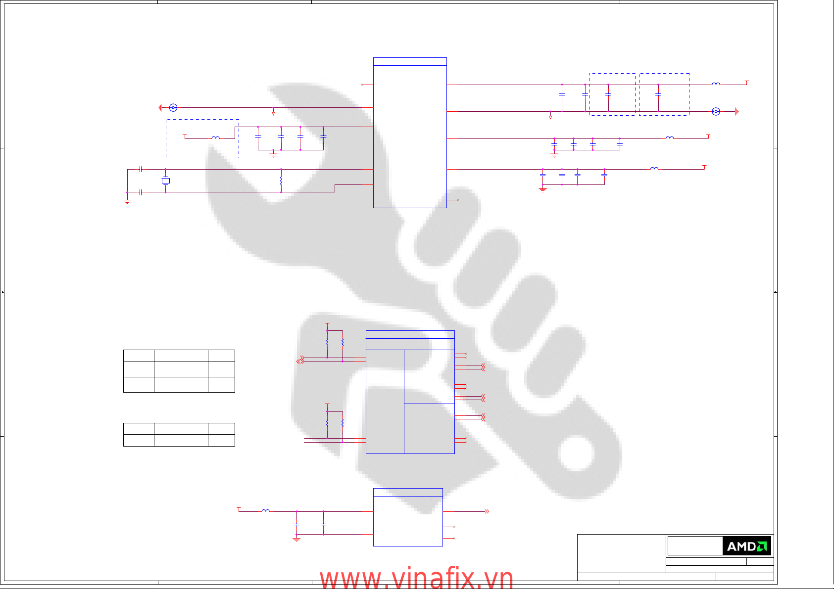
PART 4 OF 10
PART 4 OF 10
POWER
POWER
3
PCIE_VDDR#1
PCIE_VDDR#2
PCIE_VDDR#3
PCIE_VDDR#4
PCIE_VDDR#5
PCIE_VDDR#6
PCIE_VDDR#7
PCIE_VDDR#8
PCIE_VDDC#1
PCIE_VDDC#2
PCIE_VDDC#3
PCIE_VDDC#4
PCIE_VDDC#5
PCIE_VDDC#6
PCIE_VDDC#7
PCIE_VDDC#8
PCIE_VDDC#9
PCIE_VDDC#10
PCIE_VDDC#11
PCIE_VDDC#12
VDDC#1
VDDC#2
VDDC#3
VDDC#4
VDDC#5
VDDC#6
VDDC#7
VDDC#8
VDDC#9
VDDC#10
VDDC#11
VDDC#12
VDDC#13
VDDC#14
VDDC#15
VDDC#16
VDDC#17
VDDC#18
VDDC#19
VDDC#20
VDDC#21
VDDC#22
VDDC#23
VDDC#24
VDDC#25
VDDCI#1
VDDCI#2
VDDCI#3
VDDCI#4
VDDCI#5
VDDCI#6
VDDCI#7
VDDCI#8
AB23
AC23
AD24
AE24
AE25
AE26
AF25
AG26
L23
L24
L25
L26
M22
N22
N23
N24
R22
T22
U22
V22
AA15
M11
M12
N15
N17
R13
R16
R18
R21
T12
T15
T17
T20
U13
U16
U18
U21
V15
V17
V20
V21
Y13
Y16
Y18
Y21
M13
M15
M16
M17
M18
M20
M21
N20
C143
C143
1uF_6.3V
1uF_6.3V
+VDDC
C86
C86
100nF
100nF
C144
C144
1uF_6.3V
1uF_6.3V
C150
C150
1uF_6.3V
1uF_6.3V
+VDDCI+VDDCI
C87
C87
100nF
100nF
C145
C145
1uF_6.3V
1uF_6.3V
C151
C151
1uF_6.3V
1uF_6.3V
C193
C193
100nF
100nF
C146
C146
1uF_6.3V
1uF_6.3V
C152
C152
1uF_6.3V
1uF_6.3V
C168
C168
1uF_6.3V
1uF_6.3V
C194
C194
1uF_6.3V
1uF_6.3V
C149
C149
100nF
100nF
C153
C153
1uF_6.3V
1uF_6.3V
C169
C169
1uF_6.3V
1uF_6.3V
C195
C195
1uF_6.3V
1uF_6.3V
2
C148
C148
10nF
10nF
C154
C154
1uF_6.3V
1uF_6.3V
C170
C170
1uF_6.3V
1uF_6.3V
+1.8V
C155
C155
1uF_6.3V
1uF_6.3V
C171
C171
1uF_6.3V
1uF_6.3V
MC196
MC196
4.7uF_6.3V
4.7uF_6.3V
C156
C156
1uF_6.3V
1uF_6.3V
C172
C172
1uF_6.3V
1uF_6.3V
MC147
MC147
4.7uF_6.3V
4.7uF_6.3V
+1.1V
C157
C157
1uF_6.3V
1uF_6.3V
B28 220R_2AB28 220R_2A
C173
C173
1uF_6.3V
1uF_6.3V
+VDDC
C85
C85
1uF_6.3V
1uF_6.3V
MC158
MC158
4.7uF_6.3V
4.7uF_6.3V
+VDDC
1
C183
C183
1uF_6.3V
1uF_6.3V
C175
C175
10uF_X6S
10uF_X6S
MC175
MC175
4.7uF_6.3V
4.7uF_6.3V
C184
1uF_6.3V
1uF_6.3V
1uF_6.3V
1uF_6.3V
C177
C176
C176
10uF_X6S
10uF_X6S
MC176
MC176
4.7uF_6.3V
4.7uF_6.3V
2
C177
10uF_X6S
10uF_X6S
MC177
MC177
4.7uF_6.3V
4.7uF_6.3V
CONFIDENTIAL & PROPRIETARY TO ADVANCED MICRO DEVICES INC.
CONFIDENTIAL & PROPRIETARY TO ADVANCED MICRO DEVICES INC.
CONFIDENTIAL & PROPRIETARY TO ADVANCED MICRO DEVICES INC.
?2007 Advanced Micro Devices
?2007 Advanced Micro Devices
?2007 Advanced Micro Devices
This AMD Board schematic and design is the exclusive property of AMD,
This AMD Board schematic and design is the exclusive property of AMD,
This AMD Board schematic and design is the exclusive property of AMD,
and is provided only to entities under a non-disclosure agreement
and is provided only to entities under a non-disclosure agreement
and is provided only to entities under a non-disclosure agreement
with AMD for evaluation purposes. Further distribution or disclosure
with AMD for evaluation purposes. Further distribution or disclosure
with AMD for evaluation purposes. Further distribution or disclosure
is strictly prohibited. Use of this schematic and design for any purpose
is strictly prohibited. Use of this schematic and design for any purpose
is strictly prohibited. Use of this schematic and design for any purpose
other than evaluation requires a Board Technology License Agreement
other than evaluation requires a Board Technology License Agreement
other than evaluation requires a Board Technology License Agreement
with AMD. AMD makes no representations or warranties of any kind
with AMD. AMD makes no representations or warranties of any kind
with AMD. AMD makes no representations or warranties of any kind
regarding this schematic and design, including, not limited to,
regarding this schematic and design, including, not limited to,
regarding this schematic and design, including, not limited to,
any implied warranty of merchantibility or fitness for a particular
any implied warranty of merchantibility or fitness for a particular
any implied warranty of merchantibility or fitness for a particular
purpose, and disclaims responsibility forany consequences resulting
purpose, and disclaims responsibility forany consequences resulting
purpose, and disclaims responsibility forany consequences resulting
from use of the information included herein.
from use of the information included herein.
from use of the information included herein.
Title
Title
Title
RH LP RV710 DDR2 VGA (header) TVO DVI
RH LP RV710 DDR2 VGA (header) TVO DVI
RH LP RV710 DDR2 VGA (header) TVO DVI
C182
C182
1uF_6.3V
1uF_6.3V
C174
C174
10uF_X6S
10uF_X6S
MC174
MC174
4.7uF_6.3V
4.7uF_6.3V
A A
5
4
www.vinafix.vn
3
C186
C186
1uF_6.3V
1uF_6.3V
C196
C196
22uF
22uF
C187
C187
1uF_6.3V
1uF_6.3V
C197
C197
22uF
22uF
+VDDC
C188
C188
1uF_6.3V
1uF_6.3V
Advanced Micro Devices Inc.
Advanced Micro Devices Inc.
Advanced Micro Devices Inc.
1 Commerce Valley Drive East
1 Commerce Valley Drive East
1 Commerce Valley Drive East
Markham, Ontario
Markham, Ontario
Markham, Ontario
Sheet
Sheet
Sheet
C190
C190
C189
C189
1uF_6.3V
1uF_6.3V
1uF_6.3V
1uF_6.3V
Thursday, October 23, 2008
Thursday, October 23, 2008
Thursday, October 23, 2008
of
822
of
822
of
822
1
Doc No.
Doc No.
Doc No.
105-B750XX-00A
105-B750XX-00A
105-B750XX-00A
RevDate:
RevDate:
RevDate:
0
0
0
C185
C185
C184
Page 9

5
U1E
U1E
AA27
PCIE_VSS#1
AB24
PCIE_VSS#2
AB32
D D
C C
B B
PCIE_VSS#3
AC24
PCIE_VSS#4
AC26
PCIE_VSS#5
AC27
PCIE_VSS#6
AD25
PCIE_VSS#7
AD32
PCIE_VSS#8
AE27
PCIE_VSS#9
AF32
PCIE_VSS#10
AG27
PCIE_VSS#11
AH32
PCIE_VSS#12
K28
PCIE_VSS#13
K32
PCIE_VSS#14
L27
PCIE_VSS#15
M32
PCIE_VSS#16
N25
PCIE_VSS#17
N27
PCIE_VSS#18
P25
PCIE_VSS#19
P32
PCIE_VSS#20
R27
PCIE_VSS#21
T25
PCIE_VSS#22
T32
PCIE_VSS#23
U25
PCIE_VSS#24
U27
PCIE_VSS#25
V32
PCIE_VSS#26
W25
PCIE_VSS#27
W26
PCIE_VSS#28
W27
PCIE_VSS#29
Y25
PCIE_VSS#30
Y32
PCIE_VSS#31
A3
GND#1
A30
GND#2
AA13
GND#3
AA16
GND#4
AB10
GND#5
AB15
GND#6
AB6
GND#7
AC9
GND#8
AD6
GND#9
AD8
GND#10
AE7
GND#11
AG12
GND#12
AH10
GND#13
AH28
GND#14
B10
GND#15
B12
GND#16
B14
GND#17
B16
GND#18
B18
GND#19
B20
GND#20
B22
GND#21
B24
GND#22
B26
GND#23
B6
GND#24
B8
GND#25
C1
GND#26
C32
GND#27
E28
GND#28
F10
GND#29
F12
GND#30
F14
GND#31
F16
GND#32
RV710_03_20_FINAL1
RV710_03_20_FINAL1
4
PART 5 OF 10
PART 5 OF 10
GND
GND
GND#33
GND#34
GND#35
GND#36
GND#37
GND#38
GND#39
GND#40
GND#41
GND#42
GND#43
GND#44
GND#45
GND#46
GND#47
GND#48
GND#49
GND#50
GND#51
GND#52
GND#53
GND#54
GND#55
GND#56
GND#57
GND#58
GND#59
GND#60
GND#61
GND#62
GND#63
GND#64
GND#65
GND#66
GND#67
GND#68
GND#69
GND#70
GND#71
GND#72
GND#73
GND#74
GND#75
GND#76
GND#77
GND#78
GND#79
GND#80
GND#81
GND#82
GND#83
GND#84
GND#85
GND#86
GND#87
GND#88
GND#89
VSS_MECH#1
VSS_MECH#2
VSS_MECH#3
F18
F2
F20
F22
F24
F26
F6
F8
G10
G27
G31
G8
H14
H17
H2
H20
H6
J27
J31
K11
K2
K22
K6
M6
N11
N12
N13
N16
N18
N21
P6
P9
R12
R15
R17
R20
T13
T16
T18
T21
T6
U15
U17
U20
U3
U9
V13
V16
V18
V6
Y10
Y15
Y17
Y20
Y6
T11
R11
A32
AM1
AM32
3
2
1
A A
5
4
3
CONFIDENTIAL & PROPRIETARY TO ADVANCED MICRO DEVICES INC.
CONFIDENTIAL & PROPRIETARY TO ADVANCED MICRO DEVICES INC.
CONFIDENTIAL & PROPRIETARY TO ADVANCED MICRO DEVICES INC.
?2007 Advanced Micro Devices
?2007 Advanced Micro Devices
?2007 Advanced Micro Devices
This AMD Board schematic and design is the exclusive property of AMD,
This AMD Board schematic and design is the exclusive property of AMD,
This AMD Board schematic and design is the exclusive property of AMD,
and is provided only to entities under a non-disclosure agreement
and is provided only to entities under a non-disclosure agreement
and is provided only to entities under a non-disclosure agreement
with AMD for evaluation purposes. Further distribution or disclosure
with AMD for evaluation purposes. Further distribution or disclosure
with AMD for evaluation purposes. Further distribution or disclosure
is strictly prohibited. Use of this schematic and design for any purpose
is strictly prohibited. Use of this schematic and design for any purpose
is strictly prohibited. Use of this schematic and design for any purpose
other than evaluation requires a Board Technology License Agreement
other than evaluation requires a Board Technology License Agreement
other than evaluation requires a Board Technology License Agreement
with AMD. AMD makes no representations or warranties of any kind
with AMD. AMD makes no representations or warranties of any kind
with AMD. AMD makes no representations or warranties of any kind
regarding this schematic and design, including, not limited to,
regarding this schematic and design, including, not limited to,
regarding this schematic and design, including, not limited to,
any implied warranty of merchantibility or fitness for a particular
any implied warranty of merchantibility or fitness for a particular
any implied warranty of merchantibility or fitness for a particular
purpose, and disclaims responsibility forany consequences resulting
purpose, and disclaims responsibility forany consequences resulting
purpose, and disclaims responsibility forany consequences resulting
from use of the information included herein.
from use of the information included herein.
from use of the information included herein.
Title
Title
Title
RH LP RV710 DDR2 VGA (header) TVO DVI
RH LP RV710 DDR2 VGA (header) TVO DVI
RH LP RV710 DDR2 VGA (header) TVO DVI
2
Advanced Micro Devices Inc.
Advanced Micro Devices Inc.
Advanced Micro Devices Inc.
1 Commerce Valley Drive East
1 Commerce Valley Drive East
1 Commerce Valley Drive East
Markham, Ontario
Markham, Ontario
Markham, Ontario
Thursday, October 23, 2008
Thursday, October 23, 2008
Thursday, October 23, 2008
Sheet
Sheet
Sheet
of
922
of
922
of
922
Doc No.
Doc No.
Doc No.
105-B750XX-00A
105-B750XX-00A
105-B750XX-00A
1
RevDate:
RevDate:
RevDate:
0
0
0
www.vinafix.vn
Page 10

5
4
3
2
1
PIN BASED STRAPS
D D
DNI
DNI
DNI
DNI
DNI
MR45 10KMR45 10K
MR46 10KMR46 10K
MR47 10KMR47 10K
MR48 10KMR48 10K
MR49 10KMR49 10K
MR50 10KMR50 10K
MR51 10KMR51 10K
Pull-Down Resistors are for BU until built-in pull-downs are verified.
Overlap pads to save space
and to prevent assembly of
both resistors.
Layout
High logic voltageGround
C C
Signal
+3.3V
DNI
DNI
R45 10KR45 10K
R46 10KR46 10K
R47 10KR47 10K
R48 10KR48 10K
R49 10KR49 10K
R50 10KR50 10K
R51 10KR51 10K
R52 10KR52 10K
MR52 10KMR52 10K
DNI
DNI
DNI
NTSC
R53 10KR53 10K
R54 10KR54 10K
R55 10KR55 10K
R57 10KR57 10K
MR53 10KMR53 10K
MR54 10KMR54 10K
B B
MR55 10KMR55 10K
MR57 10KMR57 10K
PIN BASED STRAPS
GPIO_0
GPIO_0 (3)
GPIO_1
GPIO_1 (3)
GPIO_2
GPIO_2 (3)
GPIO_11
GPIO_11 (3)
GPIO_13
GPIO_13 (3)
GPIO_12
GPIO_12 (3)
A_VSYNC_DAC1 (3,16)
A_HSYNC_DAC1 (3,16)
GPIO_8
GPIO_8 (3)
GPIO_5
GPIO_5 (3)
GPIO_16
GPIO_16 (3)
GPIO_7
GPIO_7 (3)
VIP_DEVICE_STRAP_EN
0: Driver would ignore the value sampled on VHAD_0 during reset
1: Driver would use the value sampled at reset from VHAD_0 to determine
whether or not a VIP slave device (e.g. Theater chip) is connected
(i.e. 0 indicates yes, 1 indicates no).
VGA DISABLE : 1 for disable (set to 0 for normal operation)
GPIO(0) - TX_PWRS_ENB (Transmitter Power Savings Enable)
0: 50% Tx output swing for mobile mode
1: full Tx output swing (Default setting for Desktop)
GPIO(1) - TX_DEEMPH_EN (Transmitter De-emphasis Enable)
0: Tx de-emphasis disabled for mobile mode
1: Tx de-emphasis enabled (Default setting for Desktop)
GPIO(2) - BIF_GEN2_EN (5.0 GT/s Enable)
0 : Default. (Driver Controlled Gen2)
1 : Strap Controlled Gen2
GPIO(13, 12,11) - CONFIG[2..0]
CONFIG[2]
CONFIG[1]
CONFIG[0]
AUD[0]
AUD[1]
BIF_CLK_PM_EN
0 - Disable CLKREQ# power management capability
1 - Enable CLKREQ# power management capability
100 - 512Kbit M25P05A (ST)
101 - 1Mbit M25P10A (ST)
101 - 2Mbit M25P20 (ST)
101 - 4Mbit M25P40 (ST)
101 - 8Mbit M25P80 (ST)
100 - 512Kbit Pm25LV512 (Chingis)
101 - 1Mbit Pm25LV010 (Chingis)
[GPIO_5 : GPIO_16]
Quimonda [0:0]
Hynix [0:1]
Samsung [1:0]
RESERVED :Internal use only. Other logic must not affect this signal
during RESET.
TV OUT STANDARD
0 - PAL TVO
1 - NTSC TVO
A A
5
4
3
CONFIDENTIAL & PROPRIETARY TO ADVANCED MICRO DEVICES INC.
CONFIDENTIAL & PROPRIETARY TO ADVANCED MICRO DEVICES INC.
CONFIDENTIAL & PROPRIETARY TO ADVANCED MICRO DEVICES INC.
?2007 Advanced Micro Devices
?2007 Advanced Micro Devices
?2007 Advanced Micro Devices
This AMD Board schematic and design is the exclusive property of AMD,
This AMD Board schematic and design is the exclusive property of AMD,
This AMD Board schematic and design is the exclusive property of AMD,
and is provided only to entities under a non-disclosure agreement
and is provided only to entities under a non-disclosure agreement
and is provided only to entities under a non-disclosure agreement
with AMD for evaluation purposes. Further distribution or disclosure
with AMD for evaluation purposes. Further distribution or disclosure
with AMD for evaluation purposes. Further distribution or disclosure
is strictly prohibited. Use of this schematic and design for any purpose
is strictly prohibited. Use of this schematic and design for any purpose
is strictly prohibited. Use of this schematic and design for any purpose
other than evaluation requires a Board Technology License Agreement
other than evaluation requires a Board Technology License Agreement
other than evaluation requires a Board Technology License Agreement
with AMD. AMD makes no representations or warranties of any kind
with AMD. AMD makes no representations or warranties of any kind
with AMD. AMD makes no representations or warranties of any kind
regarding this schematic and design, including, not limited to,
regarding this schematic and design, including, not limited to,
regarding this schematic and design, including, not limited to,
any implied warranty of merchantibility or fitness for a particular
any implied warranty of merchantibility or fitness for a particular
any implied warranty of merchantibility or fitness for a particular
purpose, and disclaims responsibility forany consequences resulting
purpose, and disclaims responsibility forany consequences resulting
purpose, and disclaims responsibility forany consequences resulting
from use of the information included herein.
from use of the information included herein.
from use of the information included herein.
Title
Title
Title
RH LP RV710 DDR2 VGA (header) TVO DVI
RH LP RV710 DDR2 VGA (header) TVO DVI
RH LP RV710 DDR2 VGA (header) TVO DVI
2
Advanced Micro Devices Inc.
Advanced Micro Devices Inc.
Advanced Micro Devices Inc.
1 Commerce Valley Drive East
1 Commerce Valley Drive East
1 Commerce Valley Drive East
Markham, Ontario
Markham, Ontario
Markham, Ontario
Thursday, October 23, 2008
Thursday, October 23, 2008
Thursday, October 23, 2008
Sheet
Sheet
Sheet
of
10 22
of
10 22
of
10 22
Doc No.
Doc No.
Doc No.
105-B750XX-00A
105-B750XX-00A
105-B750XX-00A
1
RevDate:
RevDate:
RevDate:
0
0
0
www.vinafix.vn
Page 11

8
D D
7
6
5
4
3
2
1
EC116
EC116
10uF
10uF
EC1532
EC1532
1.0uF
1.0uF
EC1688
EC1688
2200p
2200p
EC1149
EC1149
10uF
10uF
ER1686
ER1686
1.87K
1.87K
+12V_BUS
EC117
EC117
10uF
10uF
0 Ohm (DNI)
0 Ohm (DNI)
12
EC1146
EC1146
10uF
10uF
ER7
ER7
B701
B701
SMD 1uH
SMD 1uH
EC301
EC301
470UF
470UF
EC323
EC323
820uF_2.5V
820uF_2.5V
+VDDC
EC321
EC321
820uF_2.5V
820uF_2.5V
+1.1V
EB620REB62
0R
+12V_BUS
ER1593
ER1593
2R2
2R2
ED28
C C
B B
A A
ED28
BAT54SLT1
BAT54SLT1
ER1800
ER1800
1 R
1 R
EC1800
EC1800
1000p
1000p
G
ER6
ER6
DNI
DNI
G
ER9
ER9
28k
EC1690
EC1690
EQ106
EQ106
2N7002
2N7002
15pF
15pF
28k
6800p
6800p
Core Power Delay
INFINEON/IPD090N03LG
INFINEON/IPD090N03LG
DS
EQ28
EQ28
DS
EQ31
EQ31
INFINEON/IPD090N03LG
INFINEON/IPD090N03LG
ER5
ER5
4.42K
4.42K
EC1691
EC1691
EL21
EL21
Dip 1.6uH
Dip 1.6uH
PHASE
0R
ER15940RER1594
0R
0R
8
7
OPS
6
FB
SS_VDDC3
5
EC143
EC143
0.1uF
0.1uF
EC3
EC3
0.1uF
0.1uF
ER15920RER1592
EMU31
EMU31
1
BOOT
2
UGATE
3
GND
LGATE4VCC
uP6101BS8-A
uP6101BS8-A
ER16180RER1618
ER8
ER8
+12V_BUS
10K
10K
+12V_BUS+3.3V_BUS
ER14
ER15
ER15
10K
10K
ER16
ER16
3.9K
3.9K
ER14
10K
10K
Q992
Q992
1
MMBT3904
MMBT3904
2 3
DS
G
CONFIDENTIAL & PROPRIETARY TO ADVANCED MICRO DEVICES INC.
CONFIDENTIAL & PROPRIETARY TO ADVANCED MICRO DEVICES INC.
CONFIDENTIAL & PROPRIETARY TO ADVANCED MICRO DEVICES INC.
?2007 Advanced Micro Devices
?2007 Advanced Micro Devices
?2007 Advanced Micro Devices
This AMD Board schematic and design is the exclusive property of AMD,
This AMD Board schematic and design is the exclusive property of AMD,
This AMD Board schematic and design is the exclusive property of AMD,
and is provided only to entities under a non-disclosure agreement
and is provided only to entities under a non-disclosure agreement
and is provided only to entities under a non-disclosure agreement
with AMD for evaluation purposes. Further distribution or disclosure
with AMD for evaluation purposes. Further distribution or disclosure
with AMD for evaluation purposes. Further distribution or disclosure
is strictly prohibited. Use of this schematic and design for any purpose
is strictly prohibited. Use of this schematic and design for any purpose
is strictly prohibited. Use of this schematic and design for any purpose
other than evaluation requires a Board Technology License Agreement
other than evaluation requires a Board Technology License Agreement
other than evaluation requires a Board Technology License Agreement
with AMD. AMD makes no representations or warranties of any kind
with AMD. AMD makes no representations or warranties of any kind
with AMD. AMD makes no representations or warranties of any kind
regarding this schematic and design, including, not limited to,
regarding this schematic and design, including, not limited to,
regarding this schematic and design, including, not limited to,
any implied warranty of merchantibility or fitness for a particular
any implied warranty of merchantibility or fitness for a particular
any implied warranty of merchantibility or fitness for a particular
purpose, and disclaims responsibility forany consequences resulting
purpose, and disclaims responsibility forany consequences resulting
purpose, and disclaims responsibility forany consequences resulting
from use of the information included herein.
from use of the information included herein.
from use of the information included herein.
Title
Title
Title
RH LP RV710 DDR2 VGA (header) TVO DVI
RH LP RV710 DDR2 VGA (header) TVO DVI
8
7
6
5
4
3
RH LP RV710 DDR2 VGA (header) TVO DVI
2
Advanced Micro Devices Inc.
Advanced Micro Devices Inc.
Advanced Micro Devices Inc.
1 Commerce Valley Drive East
1 Commerce Valley Drive East
1 Commerce Valley Drive East
Markham, Ontario
Markham, Ontario
Markham, Ontario
Thursday, October 23, 2008
Thursday, October 23, 2008
Thursday, October 23, 2008
Sheet
Sheet
Sheet
of
11 22
of
11 22
of
11 22
Doc No.
Doc No.
Doc No.
105-B750XX-00A
105-B750XX-00A
105-B750XX-00A
1
RevDate:
RevDate:
RevDate:
0
0
0
www.vinafix.vn
Page 12

8
D D
C C
ER191KER19
1K
ER18
ER18
10K
10K
1
+12V_BUS
+12V_BUS+VDDC
Q993
Q993
MMBT3904
MMBT3904
2 3
ER309
ER309
2R2
2R2
BAT54SLT1
BAT54SLT1
ER17
ER17
10K
10K
7
ED2
ED2
EC124
EC124
ER15960RER1596
0R
0.1uF
0.1uF
ER3070RER307
0R
EMU42
EMU42
1
BOOT
2
UGATE
3
GND
LGATE4VCC
uP6101BS8-A
uP6101BS8-A
ER20
ER20
10K
10K
DS
EQ107
EQ107
G
2N7002
2N7002
PHASE
ER3080RER308
0R
OPS
FB
EC168
EC168
0.1uF
0.1uF
8
7
6
5
EC1692
EC1692
6
ER18011RER1801
1R
EC1801
EC1801
1000p
1000p
EQ36
EQ36
1234
APM3023 SOT223
APM3023 SOT223
ER10
ER10
DNI
DNI
EQ37
EQ37
1234
APM3023 SOT223
APM3023 SOT223
ER12
ER12
1.87K
ER21
ER21
20k
20k
EC1693
EC1693
1.87K
EC7
EC7
DNI
DNI
ER13
ER13
1.2K
1.2K
10p
10p
0.022u
0.022u
ER11
ER11
DNI
DNI
EL64
EL64
Dip 1.6uH
Dip 1.6uH
5
EC183
EC183
10uF
10uF
EC182
EC182
10uF
10uF
+12V_BUS
EC165
EC165
10uF
10uF
4
3
2
1
+MVDD = 0.8 * ( 1+ ( ER12 / ER13 ) )
12
B702
B702
Dip-1.2uH
Dip-1.2uH
EC181
EC181
10uF
10uF
+MVDD
EC160
EC160
10uF
10uF
EC169
EC169
10uF
10uF
EC805
EC805
1000uF
1000uF
Memory Power Seq
B B
+1.8V
R9981KR998
1K
R997
R997
10K
10K
A A
+12V_BUS
R1000
R1000
5.1K
5.1K
402
5%
Q998
Q998
1
MMBT3904
MMBT3904
2 3
8
R999
R999
5.1K
5.1K
+12V_BUS +3.3V_BUS
R990
R990
255K
255K
402
Q997
Q997
1
MMBT3904
MMBT3904
2 3
7
Q996
Q996
1234
R989
R989
100K
100K
C845
C845
0.1uF
0.1uF
402
X5R
16V
APM2054NVC
APM2054NVC
6.3V
1206
C1016
C1016
10uf
10uf
Y5V
+MVDD
+3.3V
+
+
12
C994
C994
C993
C993
0.1uf
0.1uf
47uF
47uF
+MVDD
C1026
C1026
10nF
ALL_RAILS_UP (16,18)
6
www.vinafix.vn
10nF
5
C1027
C1027
10nF
10nF
EC164
EC164
10uF
10uF
C1028
C1028
10nF
10nF
+3.3V
C1030
C1030
10nF
10nF
EC159
EC159
10uF
10uF
4
EC346
EC346
10uf
10uf
+3.3V +3.3V
C995
C995
C996
C996
10uf
10uf
10uf
10uf
+3.3V
C999
C999
C998
C998
1000 pF
1000 pF
1000 pF
1000 pF
Title
Title
3
Title
C997
C997
10uf
10uf
C1000
C1000
1000 pF
1000 pF
CONFIDENTIAL & PROPRIETARY TO ADVANCED MICRO DEVICES INC.
CONFIDENTIAL & PROPRIETARY TO ADVANCED MICRO DEVICES INC.
CONFIDENTIAL & PROPRIETARY TO ADVANCED MICRO DEVICES INC.
?2007 Advanced Micro Devices
?2007 Advanced Micro Devices
?2007 Advanced Micro Devices
This AMD Board schematic and design is the exclusive property of AMD,
This AMD Board schematic and design is the exclusive property of AMD,
This AMD Board schematic and design is the exclusive property of AMD,
and is provided only to entities under a non-disclosure agreement
and is provided only to entities under a non-disclosure agreement
and is provided only to entities under a non-disclosure agreement
with AMD for evaluation purposes. Further distribution or disclosure
with AMD for evaluation purposes. Further distribution or disclosure
with AMD for evaluation purposes. Further distribution or disclosure
is strictly prohibited. Use of this schematic and design for any purpose
is strictly prohibited. Use of this schematic and design for any purpose
is strictly prohibited. Use of this schematic and design for any purpose
other than evaluation requires a Board Technology License Agreement
other than evaluation requires a Board Technology License Agreement
other than evaluation requires a Board Technology License Agreement
with AMD. AMD makes no representations or warranties of any kind
with AMD. AMD makes no representations or warranties of any kind
with AMD. AMD makes no representations or warranties of any kind
regarding this schematic and design, including, not limited to,
regarding this schematic and design, including, not limited to,
regarding this schematic and design, including, not limited to,
any implied warranty of merchantibility or fitness for a particular
any implied warranty of merchantibility or fitness for a particular
any implied warranty of merchantibility or fitness for a particular
purpose, and disclaims responsibility forany consequences resulting
purpose, and disclaims responsibility forany consequences resulting
purpose, and disclaims responsibility forany consequences resulting
from use of the information included herein.
from use of the information included herein.
from use of the information included herein.
RH LP RV710 DDR2 VGA (header) TVO DVI
RH LP RV710 DDR2 VGA (header) TVO DVI
RH LP RV710 DDR2 VGA (header) TVO DVI
2
C1014
C1014
C1012
C1012
100pF
100pF
100pF
100pF
+3.3V
C1019
C1019
C1017
C1017
10nF
10nF
10nF
10nF
Advanced Micro Devices Inc.
Advanced Micro Devices Inc.
Advanced Micro Devices Inc.
1 Commerce Valley Drive East
1 Commerce Valley Drive East
1 Commerce Valley Drive East
Markham, Ontario
Markham, Ontario
Markham, Ontario
Thursday, October 23, 2008
Thursday, October 23, 2008
Thursday, October 23, 2008
Sheet
Sheet
Sheet
of
12 22
of
12 22
of
12 22
C1015
C1015
100pF
100pF
C1018
C1018
10nF
10nF
Doc No.
Doc No.
Doc No.
105-B750XX-00A
105-B750XX-00A
105-B750XX-00A
1
RevDate:
RevDate:
RevDate:
0
0
0
Page 13

5
4
3
2
1
D D
APL431BAC_SOT23
APL431BAC_SOT23
C C
+12V_BUS
EC133
EC133
10uF
10uF
+3.3V_BUS
2
U5
U5
VIN3VOUT
RC1117S_SOT223
RC1117S_SOT223
I31-01117F9-A30
ER124
ER124
15R
15R
2.5V_REF1
EC109
EC109
EREG9
EREG9
10uF_6.3V
10uF_6.3V
DNI
3 1
DNI
+5V
4
4
2
ADJ/GND
1
ER304
ER304
121
121
R11-1210T13-W08
ER305
ER305
365
365
R11-3650T13-Y01
EC135
EC135
10uF
10uF
EC134
EC134
10uF
10uF
+3.3V_BUS +1.8V
2.5V_REF1
R951
R951
383
383
R956
R956
1.5K
1.5K
R954
R954
1.2K
1.2K
R9521KR952
1K
U951_REFEN
C954
C954
1uF_6.3V
1uF_6.3V
U952_REFEN
C961
C961
1uF_6.3V
1uF_6.3V
C958
C958
1uF_6.3V
1uF_6.3V
+3.3V_BUS
D706
D706
DIODE SCHOTTKY SM32
DIODE SCHOTTKY SM32
C966
C966
1uF_6.3V
1uF_6.3V
C962
C962
10uF
10uF
C957
C957
10uF
10uF
C964
C964
10uF
10uF
C956
C956
10uF
10uF
2.5V_REF1
+1.1V
R9551KR955
1K
R9531KR953
1K
U951_VOUTU951_VIN
U951
U952
U952
1
VIN
2
GND
3
VREF
VOUT4NC
APL5331
APL5331
U951
1
VIN
2
GND
3
VREF
VOUT4NC
APL5331
APL5331
VCNTL
NC#8
NC#7
8
NC#8
7
NC#7
VCNTL
THM
8
7
6
5
9
THM
U951_VCNTL
6
5
9
U951_VCNTL
U951_VCNTL (14)
U951_VCNTL (14)
U951_VIN
C955
C965
C965
10uF
10uF
C951
C951
10uF
10uF
C960
C960
10uF
10uF
C955
10uF
10uF
C952
C952
C953
C953
10uF
10uF
22uF
22uF
U952_VOUTU952_VIN
C963
C963
C959
C959
10uF
10uF
22uF
22uF
U951_REFEN
U951_VOUT
U952_VIN
U952_REFEN
U952_VOUT
Vout=1.25V* [1+(ER305/ER304) ]
B B
A A
CONFIDENTIAL & PROPRIETARY TO ADVANCED MICRO DEVICES INC.
CONFIDENTIAL & PROPRIETARY TO ADVANCED MICRO DEVICES INC.
CONFIDENTIAL & PROPRIETARY TO ADVANCED MICRO DEVICES INC.
?2007 Advanced Micro Devices
?2007 Advanced Micro Devices
?2007 Advanced Micro Devices
This AMD Board schematic and design is the exclusive property of AMD,
This AMD Board schematic and design is the exclusive property of AMD,
This AMD Board schematic and design is the exclusive property of AMD,
and is provided only to entities under a non-disclosure agreement
and is provided only to entities under a non-disclosure agreement
and is provided only to entities under a non-disclosure agreement
with AMD for evaluation purposes. Further distribution or disclosure
with AMD for evaluation purposes. Further distribution or disclosure
with AMD for evaluation purposes. Further distribution or disclosure
is strictly prohibited. Use of this schematic and design for any purpose
is strictly prohibited. Use of this schematic and design for any purpose
is strictly prohibited. Use of this schematic and design for any purpose
other than evaluation requires a Board Technology License Agreement
other than evaluation requires a Board Technology License Agreement
other than evaluation requires a Board Technology License Agreement
with AMD. AMD makes no representations or warranties of any kind
with AMD. AMD makes no representations or warranties of any kind
with AMD. AMD makes no representations or warranties of any kind
regarding this schematic and design, including, not limited to,
regarding this schematic and design, including, not limited to,
regarding this schematic and design, including, not limited to,
any implied warranty of merchantibility or fitness for a particular
any implied warranty of merchantibility or fitness for a particular
any implied warranty of merchantibility or fitness for a particular
purpose, and disclaims responsibility forany consequences resulting
purpose, and disclaims responsibility forany consequences resulting
purpose, and disclaims responsibility forany consequences resulting
from use of the information included herein.
from use of the information included herein.
from use of the information included herein.
Title
Title
Title
RH LP RV710 DDR2 VGA (header) TVO DVI
RH LP RV710 DDR2 VGA (header) TVO DVI
5
4
www.vinafix.vn
3
2
RH LP RV710 DDR2 VGA (header) TVO DVI
Advanced Micro Devices Inc.
Advanced Micro Devices Inc.
Advanced Micro Devices Inc.
1 Commerce Valley Drive East
1 Commerce Valley Drive East
1 Commerce Valley Drive East
Markham, Ontario
Markham, Ontario
Markham, Ontario
Thursday, October 23, 2008
Thursday, October 23, 2008
Thursday, October 23, 2008
Sheet
Sheet
Sheet
of
13 22
of
13 22
of
13 22
1
Doc No.
Doc No.
Doc No.
105-B750XX-00A
105-B750XX-00A
105-B750XX-00A
RevDate:
RevDate:
RevDate:
0
0
0
Page 14

5
D D
C C
4
3
2
1
+5V
+VDDC
R8411KR841
1K
C841
C841
1uF_6.3V
1uF_6.3V
+12V_BUS
1
R843
R843
5.1K
5.1K
5%
Q840
Q840
MMBT3904
MMBT3904
2 3
R844 5.1KR844 5.1K
30
R84530R845
Q841
Q841
5%
1
MMBT3904
MMBT3904
2 3
U951_VCNTL (13)
B B
A A
CONFIDENTIAL & PROPRIETARY TO ADVANCED MICRO DEVICES INC.
CONFIDENTIAL & PROPRIETARY TO ADVANCED MICRO DEVICES INC.
CONFIDENTIAL & PROPRIETARY TO ADVANCED MICRO DEVICES INC.
?2007 Advanced Micro Devices
?2007 Advanced Micro Devices
?2007 Advanced Micro Devices
This AMD Board schematic and design is the exclusive property of AMD,
This AMD Board schematic and design is the exclusive property of AMD,
This AMD Board schematic and design is the exclusive property of AMD,
and is provided only to entities under a non-disclosure agreement
and is provided only to entities under a non-disclosure agreement
and is provided only to entities under a non-disclosure agreement
with AMD for evaluation purposes. Further distribution or disclosure
with AMD for evaluation purposes. Further distribution or disclosure
with AMD for evaluation purposes. Further distribution or disclosure
is strictly prohibited. Use of this schematic and design for any purpose
is strictly prohibited. Use of this schematic and design for any purpose
is strictly prohibited. Use of this schematic and design for any purpose
other than evaluation requires a Board Technology License Agreement
other than evaluation requires a Board Technology License Agreement
other than evaluation requires a Board Technology License Agreement
with AMD. AMD makes no representations or warranties of any kind
with AMD. AMD makes no representations or warranties of any kind
with AMD. AMD makes no representations or warranties of any kind
regarding this schematic and design, including, not limited to,
regarding this schematic and design, including, not limited to,
regarding this schematic and design, including, not limited to,
any implied warranty of merchantibility or fitness for a particular
any implied warranty of merchantibility or fitness for a particular
any implied warranty of merchantibility or fitness for a particular
purpose, and disclaims responsibility forany consequences resulting
purpose, and disclaims responsibility forany consequences resulting
purpose, and disclaims responsibility forany consequences resulting
from use of the information included herein.
from use of the information included herein.
from use of the information included herein.
Title
Title
Title
RH LP RV710 DDR2 VGA (header) TVO DVI
RH LP RV710 DDR2 VGA (header) TVO DVI
5
4
www.vinafix.vn
3
2
RH LP RV710 DDR2 VGA (header) TVO DVI
Advanced Micro Devices Inc.
Advanced Micro Devices Inc.
Advanced Micro Devices Inc.
1 Commerce Valley Drive East
1 Commerce Valley Drive East
1 Commerce Valley Drive East
Markham, Ontario
Markham, Ontario
Markham, Ontario
Thursday, October 23, 2008
Thursday, October 23, 2008
Thursday, October 23, 2008
Sheet
Sheet
Sheet
of
14 22
of
14 22
of
14 22
1
Doc No.
Doc No.
Doc No.
105-B750XX-00A
105-B750XX-00A
105-B750XX-00A
RevDate:
RevDate:
RevDate:
0
0
0
Page 15

8
7
6
5
4
3
2
1
CHANNEL A: RANK 0 512MB DDR2
MAX DENSITY: 64Mx16
M_DQMA#[7..0](7)
D D
M_MDA[63..0](7)
M_MAA[12..0](7)
C C
ODTA0(7) ODTA0(7) ODTA1(7) ODTA1(7)
VREF_A0
+MVDD +MVDD +MVDD
R201
R201
4.99K
4.99K
R202
B B
R202
4.99K
4.99K
M_DQMA#0
M_DQMA#1
M_DQMA#2
M_DQMA#3
M_DQMA#4
M_DQMA#5
M_DQMA#6
M_DQMA#7
BA0(7)
BA1(7)
BA2(7)
CLKA#0(7)
CLKA0(7)
CKEA0(7)
CSA#0_0(7)
R212 10RR212 10R
VREF_U20
C413
C413
100nF
100nF
L2
L3
L1
M_MAA12
R2
M_MAA11
P7
M_MAA10
M2
M_MAA9
P3
M_MAA8
P8
M_MAA7
P2
M_MAA6
N7
M_MAA5
N3
M_MAA4
N8
M_MAA3
N2
M_MAA2
M7
M_MAA1
M3
M_MAA0
M8
K8
J8
K2
L8
WEA#0(7)
K7
RASA#0(7)
L7
CASA#0(7)
M_DQMA#2
F3
M_DQMA#3 M_DQMA#7
B3
K9
M_QSA2
F7
E8
M_QSA3
B7
A8
J2
A2
E2
R3
R7
R8
M_QSA[7..0](7)
U201
U201
BA0
BA1
BA2
A12
A11
A10/AP
A9
A8
A7
A6
A5
A4
A3
A2
A1
A0
VDDQ1
CK
VDDQ2
CK
VDDQ3
VDDQ4
CKE
VDDQ5
VDDQ6
VDDQ7
CS
VDDQ8
VDDQ9
WEK3VDDQ10
RAS
CAS
LDM
UDM
VSSDL
ODT
LDQS
VSSQ1
LDQS
VSSQ2
VSSQ3
VSSQ4
VSSQ5
UDQS
VSSQ6
UDQS
VSSQ7
VSSQ8
VREF
VSSQ9
VSSQ10
NC#A2
NC#E2
NC#R3
NC#R7
NC#R8
23BC2347SC25
23BC2347SC25
M_QSA0
M_QSA1
M_QSA2
M_QSA3
M_QSA4
M_QSA5
M_QSA6
M_QSA7
M_MDA27
B9
DQ15
M_MDA30
B1
DQ14
M_MDA24
D9
DQ13
M_MDA29
D1
DQ12
M_MDA31 M_MAA12
D3
DQ11
M_MDA26
D7
DQ10
M_MDA28
C2
DQ9
M_MDA25
C8
DQ8
M_MDA18
F9
DQ7
M_MDA21
F1
DQ6
M_MDA17
H9
DQ5
M_MDA22
H1
DQ4
M_MDA23
H3
DQ3
M_MDA16
H7
DQ2
M_MDA20
G2
DQ1
M_MDA19
G8
DQ0
A9
C1
C3
C7
C9
E9
G1
G3
G7
G9
Possible alternate 5150005600G
A1
VDD1
E1
VDD2
J9
VDD3
M9
VDD4
R1
VDD5
VDDL
VSS1
VSS2
VSS3
VSS4
VSS5
VDDL_U20
J1
J7
C411
C411
C412
C412
100nF
100nF
1uF_6.3V
A7
B2
B8
D2
D8
E7
F2
F8
H2
H8
A3
E3
J3
N1
P9
1uF_6.3V
+MVDD
+MVDD
VREF_A0
BA0(7)
BA1(7)
BA2(7)
R213 10RR213 10R
R214 10RR214 10R
R203
R203
4.99K
4.99K
VREF_U21
R204
R204
4.99K
4.99K
M_MAA11
M_MAA10
M_MAA9
M_MAA8
M_MAA7
M_MAA6
M_MAA5
M_MAA4
M_MAA3
M_MAA2
M_MAA1
M_MAA0
CLKA#0(7)
CLKA0(7)
CKEA0(7)
CSA#0_0(7)
WEA#0(7)
RASA#0(7)
CASA#0(7)
M_DQMA#0
M_DQMA#1
M_QSA0
M_QSA1
C438
C438
100nF
100nF
U202
U202
L2
BA0
L3
BA1
L1
BA2
R2
A12
P7
A11
M2
A10/AP
P3
A9
P8
A8
P2
A7
N7
A6
N3
A5
N8
A4
N2
A3
M7
A2
M3
A1
M8
A0
K8
CK
J8
CK
K2
CKE
L8
CS
WEK3VDDQ10
K7
RAS
L7
CAS
F3
LDM
B3
UDM
K9
ODT
F7
LDQS
E8
LDQS
B7
UDQS
A8
UDQS
J2
VREF
A2
NC#A2
E2
NC#E2
R3
NC#R3
R7
NC#R7
R8
NC#R8
23BC2347SC25
23BC2347SC25
DQ15
DQ14
DQ13
DQ12
DQ11
DQ10
VDDQ1
VDDQ2
VDDQ3
VDDQ4
VDDQ5
VDDQ6
VDDQ7
VDDQ8
VDDQ9
VDD1
VDD2
VDD3
VDD4
VDD5
VDDL
VSSDL
VSSQ1
VSSQ2
VSSQ3
VSSQ4
VSSQ5
VSSQ6
VSSQ7
VSSQ8
VSSQ9
VSSQ10
VSS1
VSS2
VSS3
VSS4
VSS5
U203
M_MDA14
B9
M_MDA9
B1
M_MDA13
D9
M_MDA8
D1
M_MDA10
D3
M_MDA12
D7
M_MDA11
C2
DQ9
C8
DQ8
M_MDA4
F9
DQ7
M_MDA3
F1
DQ6
M_MDA5
H9
DQ5
M_MDA0
H1
DQ4
M_MDA1
H3
DQ3
M_MDA6
H7
DQ2
M_MDA2
G2
DQ1
M_MDA7
G8
DQ0
A9
C1
C3
C7
C9
E9
G1
G3
G7
G9
Possible alternate 5150005600G
A1
E1
J9
M9
R1
VDDL_U21
J1
J7
A7
B2
B8
D2
D8
E7
F2
F8
H2
H8
A3
E3
J3
N1
P9
C436
C436
100nF
100nF
C437
C437
1uF_6.3V
1uF_6.3V
+MVDD
+MVDD
VREF_A1
BA0(7)
BA1(7)
BA2(7)
R215 10RR215 10R
R216 10RR216 10R
R205
R205
4.99K
4.99K
VREF_U22
R206
R206
4.99K
4.99K
M_MAA12
M_MAA11
M_MAA10
M_MAA9
M_MAA8
M_MAA7
M_MAA6
M_MAA5
M_MAA4
M_MAA3
M_MAA2
M_MAA1
M_MAA0
CLKA#1(7)
CLKA1(7)
CKEA1(7)
CSA#1_0(7)
WEA#1(7)
RASA#1(7)
CASA#1(7)
M_DQMA#6
M_QSA6
M_QSA7
C463
C463
100nF
100nF
U203
L2
BA0
L3
BA1
L1
BA2
R2
A12
P7
A11
M2
A10/AP
P3
A9
P8
A8
P2
A7
N7
A6
N3
A5
N8
A4
N2
A3
M7
A2
M3
A1
M8
A0
K8
CK
J8
CK
K2
CKE
L8
CS
WEK3VDDQ10
K7
RAS
L7
CAS
F3
LDM
B3
UDM
K9
ODT
F7
LDQS
E8
LDQS
B7
UDQS
A8
UDQS
J2
VREF
A2
NC#A2
E2
NC#E2
R3
NC#R3
R7
NC#R7
R8
NC#R8
23BC2347SC25
23BC2347SC25
DQ15
DQ14
DQ13
DQ12
DQ11
DQ10
VDDQ1
VDDQ2
VDDQ3
VDDQ4
VDDQ5
VDDQ6
VDDQ7
VDDQ8
VDDQ9
VDD1
VDD2
VDD3
VDD4
VDD5
VDDL
VSSDL
VSSQ1
VSSQ2
VSSQ3
VSSQ4
VSSQ5
VSSQ6
VSSQ7
VSSQ8
VSSQ9
VSSQ10
VSS1
VSS2
VSS3
VSS4
VSS5
M_MDA58
B9
M_MDA60
B1
M_MDA57
D9
M_MDA62
D1
M_MDA61
D3
M_MDA56
D7
M_MDA63
C2
DQ9
M_MDA59M_MDA15
C8
DQ8
M_MDA51
F9
DQ7
M_MDA53
F1
DQ6
M_MDA48
H9
DQ5
M_MDA52
H1
DQ4
M_MDA55
H3
DQ3
M_MDA49
H7
DQ2
M_MDA54
G2
DQ1
M_MDA50
G8
DQ0
A9
C1
C3
C7
C9
E9
G1
G3
G7
G9
A1
E1
J9
M9
R1
VDDL_U22
J1
J7
C461
C461
100nF
100nF
A7
B2
B8
D2
D8
E7
F2
F8
H2
H8
A3
E3
J3
N1
P9
C462
C462
1uF_6.3V
1uF_6.3V
+MVDD
+MVDD
VREF_A1
+MVDD
BA0(7)
BA1(7)
BA2(7)
R217 10RR217 10RR211 10RR211 10R
R218 10RR218 10R
R207
R207
4.99K
4.99K
VREF_U23
R208
R208
4.99K
4.99K
M_MAA12
M_MAA11
M_MAA10
M_MAA9
M_MAA8
M_MAA7
M_MAA6
M_MAA5
M_MAA4
M_MAA3
M_MAA2
M_MAA1
M_MAA0
CLKA#1(7)
CLKA1(7)
CKEA1(7)
CSA#1_0(7)
WEA#1(7)
RASA#1(7)
CASA#1(7)
M_DQMA#4
M_DQMA#5
M_QSA4
M_QSA5
C448
C448
100nF
100nF
U204
U204
L2
BA0
L3
BA1
L1
BA2
R2
A12
P7
A11
M2
A10/AP
P3
A9
P8
A8
P2
A7
N7
A6
N3
A5
N8
A4
N2
A3
M7
A2
M3
A1
M8
A0
K8
CK
J8
CK
K2
CKE
L8
CS
WEK3VDDQ10
K7
RAS
L7
CAS
F3
LDM
B3
UDM
K9
ODT
F7
LDQS
E8
LDQS
B7
UDQS
A8
UDQS
J2
VREF
A2
NC#A2
E2
NC#E2
R3
NC#R3
R7
NC#R7
R8
NC#R8
23BC2347SC25
23BC2347SC25
DQ15
DQ14
DQ13
DQ12
DQ11
DQ10
VDDQ1
VDDQ2
VDDQ3
VDDQ4
VDDQ5
VDDQ6
VDDQ7
VDDQ8
VDDQ9
VDD1
VDD2
VDD3
VDD4
VDD5
VDDL
VSSDL
VSSQ1
VSSQ2
VSSQ3
VSSQ4
VSSQ5
VSSQ6
VSSQ7
VSSQ8
VSSQ9
VSSQ10
VSS1
VSS2
VSS3
VSS4
VSS5
M_MDA46
B9
M_MDA40
B1
M_MDA45
D9
M_MDA43
D1
M_MDA41
D3
M_MDA47
D7
M_MDA42
C2
DQ9
M_MDA44
C8
DQ8
M_MDA36
F9
DQ7
M_MDA34
F1
DQ6
M_MDA37
H9
DQ5
M_MDA32
H1
DQ4
M_MDA33
H3
DQ3
M_MDA39
H7
DQ2
M_MDA35
G2
DQ1
M_MDA38
G8
DQ0
A9
C1
C3
C7
C9
E9
G1
G3
G7
G9
A1
E1
J9
M9
R1
J1
J7
A7
B2
B8
D2
D8
E7
F2
F8
H2
H8
A3
E3
J3
N1
P9
VDDL_U23
C446
C446
100nF
100nF
C447
C447
1uF_6.3V
1uF_6.3V
+MVDD
+MVDD
+MVDD
C401
C401
C402
C402
C403
1uF_6.3V
1uF_6.3V
+MVDD
C406
C406
1uF_6.3V
1uF_6.3V
402
A A
8
C403
1uF_6.3V
1uF_6.3V
1uF_6.3V
1uF_6.3V
402402402
C408
C408
C407
C407
1uF_6.3V
1uF_6.3V
1uF_6.3V
1uF_6.3V
402 402 402
7
C409
C409
1uF_6.3V
1uF_6.3V
C410
C410
1uF_6.3V
1uF_6.3V
402
CLKA0(7)
CLKA#0(7)
CLKA1(7)
CLKA#1(7)
R221
R221
56R
56R
402
R222
R222
56R
56R
402 402
R223
R223
56R
56R
402
R224
R224
56R
56R
402 402
6
+MVDD
C427
C427
C428
C426
C426
1uF_6.3V
1uF_6.3V
402 402402
+MVDD
C431
C431
1uF_6.3V
1uF_6.3V
402 402
C499
C499
10nF
10nF
C500
C500
10nF
10nF
C428
1uF_6.3V
1uF_6.3V
1uF_6.3V
1uF_6.3V
C433
C433
C432
C432
1uF_6.3V
1uF_6.3V
402 402 402 402
C434
C434
1uF_6.3V
1uF_6.3V
1uF_6.3V
1uF_6.3V
+MVDD +MVDD
R209
R209
4.99K
4.99K
VREF_A0 VREF_A1
R210
R210
4.99K
4.99K
5
C435
C435
1uF_6.3V
1uF_6.3V
R219
R219
4.99K
4.99K
R220
R220
4.99K
4.99K
+MVDD
C451
C451
C452
C452
C453
1uF_6.3V
1uF_6.3V
402 402402
+MVDD
C456
C456
1uF_6.3V
1uF_6.3V
4
C453
1uF_6.3V
1uF_6.3V
1uF_6.3V
1uF_6.3V
C457
C457
C458
C458
1uF_6.3V
1uF_6.3V
1uF_6.3V
1uF_6.3V
402 402 402
C459
C459
1uF_6.3V
1uF_6.3V
C460
C460
1uF_6.3V
1uF_6.3V
402
CONFIDENTIAL & PROPRIETARY TO ADVANCED MICRO DEVICES INC.
CONFIDENTIAL & PROPRIETARY TO ADVANCED MICRO DEVICES INC.
CONFIDENTIAL & PROPRIETARY TO ADVANCED MICRO DEVICES INC.
?2007 Advanced Micro Devices
?2007 Advanced Micro Devices
?2007 Advanced Micro Devices
This AMD Board schematic and design is the exclusive property of AMD,
This AMD Board schematic and design is the exclusive property of AMD,
This AMD Board schematic and design is the exclusive property of AMD,
and is provided only to entities under a non-disclosure agreement
and is provided only to entities under a non-disclosure agreement
and is provided only to entities under a non-disclosure agreement
with AMD for evaluation purposes. Further distribution or disclosure
with AMD for evaluation purposes. Further distribution or disclosure
with AMD for evaluation purposes. Further distribution or disclosure
is strictly prohibited. Use of this schematic and design for any purpose
is strictly prohibited. Use of this schematic and design for any purpose
is strictly prohibited. Use of this schematic and design for any purpose
other than evaluation requires a Board Technology License Agreement
other than evaluation requires a Board Technology License Agreement
other than evaluation requires a Board Technology License Agreement
with AMD. AMD makes no representations or warranties of any kind
with AMD. AMD makes no representations or warranties of any kind
with AMD. AMD makes no representations or warranties of any kind
regarding this schematic and design, including, not limited to,
regarding this schematic and design, including, not limited to,
regarding this schematic and design, including, not limited to,
any implied warranty of merchantibility or fitness for a particular
any implied warranty of merchantibility or fitness for a particular
any implied warranty of merchantibility or fitness for a particular
purpose, and disclaims responsibility forany consequences resulting
purpose, and disclaims responsibility forany consequences resulting
purpose, and disclaims responsibility forany consequences resulting
from use of the information included herein.
from use of the information included herein.
from use of the information included herein.
Title
Title
Title
RH LP RV710 DDR2 VGA (header) TVO DVI
RH LP RV710 DDR2 VGA (header) TVO DVI
3
RH LP RV710 DDR2 VGA (header) TVO DVI
+MVDD
C476
C476
C477
C477
C478
1uF_6.3V
1uF_6.3V
402 402402
+MVDD
C481
C481
1uF_6.3V
1uF_6.3V
402
2
C478
1uF_6.3V
1uF_6.3V
1uF_6.3V
1uF_6.3V
C483
C483
C484
C482
C482
1uF_6.3V
1uF_6.3V
402 402 402 402
Advanced Micro Devices Inc.
Advanced Micro Devices Inc.
Advanced Micro Devices Inc.
1 Commerce Valley Drive East
1 Commerce Valley Drive East
1 Commerce Valley Drive East
Markham, Ontario
Markham, Ontario
Markham, Ontario
Sheet
Sheet
Sheet
C484
1uF_6.3V
1uF_6.3V
1uF_6.3V
1uF_6.3V
Thursday, October 23, 2008
Thursday, October 23, 2008
Thursday, October 23, 2008
of
15 22
of
15 22
of
15 22
Doc No.
Doc No.
Doc No.
C485
C485
1uF_6.3V
1uF_6.3V
105-B750XX-00A
105-B750XX-00A
105-B750XX-00A
1
RevDate:
RevDate:
RevDate:
0
0
0
www.vinafix.vn
Page 16

5
4
3
2
1
DAC 1 OUTPUT
+5V
+5V_VESA
EF1
EF1
0.2A
Place close to Connector
Pseudo differential RGB signals should be routed from the ASIC to the display connector without switching reference plane or running over split plane
D D
C C
Resistors are footprint options for the inductors. Footprints should be overlapped. (R1024-26)
A_R_DAC1(3)
A_RB_DAC1(3)
A_G_DAC1(3)
A_GB_DAC1(3)
A_B_DAC1(3)
A_BB_DAC1(3)
R1027
R1028
R1028
37.4R
37.4R
+5V
2 3
5 6
R1027
37.4R
37.4R
U1999A
U1999A
14
74AHCT125
74AHCT125
1
7
U1999B
U1999B
4
74AHCT125
74AHCT125
R1029
R1029
37.4R
37.4R
DDCAUX5N(4)
DDCAUX5P(4)
C1999 100nFC1999 100nF
A_HSYNC_DAC1(3,10)
A_VSYNC_DAC1(3,10)
SYNC and DDC should be routed from the ASIC to the display connector without switching reference plane or running over split plane
R1003
R1003
75R
75R
A_HSYNC_DAC1_B
A_VSYNC_DAC1_B
R1002
R1002
75R
75R
+5V
+5V
A_R_DAC1_M
L1001 8NH_500MAL1001 8NH_500MA
A_G_DAC1_M
L1002 8NH_500MAL1002 8NH_500MA
A_B_DAC1_M
L1003 8NH_500MAL1003 8NH_500MA
R1001
R1001
75R
75R
R1005
R1005
2.2K
2.2K
402
R1008
R1008
2.2K
2.2K
402 402
C1002
C1002
C1001
C1001
8.0pF
8.0pF
8.0pF
8.0pF
402 402 402
R1006 33RR1006 33R
R1009 33RR1009 33R
R1010
R1010
R1011
R1011
C1003
C1003
8.0pF
8.0pF
24R
24R
24R
24R
402
402
402
DDCDATA_DAC1_R
DDCCLK_DAC1_R
A_HSYNC_DAC1_R
A_VSYNC_DAC1_R
A_R_DAC1_F
A_G_DAC1_F
A_B_DAC1_F
C1004
C1004
C1005
C1005
C1006
C1006
8.0pF
8.0pF
8.0pF
8.0pF
8.0pF
8.0pF
BAT54SLT1
BAT54SLT1
+3.3V +3.3V+3.3V
BAT54SLT1
BAT54SLT1
ED62
ED62
DDCDATA_DAC1_R
DDCCLK_DAC1_R
A_HSYNC_DAC1_R
A_VSYNC_DAC1_R
DDCDATA_DAC1_R
DDCCLK_DAC1_R
A_HSYNC_DAC1_R
A_VSYNC_DAC1_R
A_R_DAC1_F
A_G_DAC1_F
A_B_DAC1_F
ED63
ED63
To DVI connector.
BAT54SLT1
BAT54SLT1
0.2A
ED64
ED64
MJ1001
MJ1001
1
R
2
G
3
B
11
MS0
12
MS1
4
MS2
15
MS3
9
NC
13
HS
14
VS
5
VSS
6
VSS#6
7
C1010
C1010
68pF
68pF
VSS#7
8
VSS#8
10
VSS#10
16
CASE
17
CASE#17
G3179C219-005
G3179C219-005
DPE / DPF OUTPUT
B B
C1602 100nF_6.3VC1602 100nF_6.3V
C1604 100nF_6.3VC1604 100nF_6.3V
C1606 100nF_6.3VC1606 100nF_6.3V
C1608 100nF_6.3VC1608 100nF_6.3V
C1610 100nF_6.3VC1610 100nF_6.3V
C1612 100nF_6.3VC1612 100nF_6.3V
C1614 100nF_6.3VC1614 100nF_6.3V
5
R1601 499RR1601 499R
R1602 499RR1602 499R
R1605 499RR1605 499R
R1606 499RR1606 499R
R1609 499RR1609 499R
R1610 499RR1610 499R
R1612 499RR1612 499R
T2X2M_C
Q1602
Q1602
MMBT3904
MMBT3904
T2X2P_C
T2X4M_C
T2X4P_C
DDCCLK_DAC1_R
DDCDATA_DAC1_R
A_VSYNC_DAC1_R
T2X1M_C
T2X1P_C
T2X3M_C
T2X3P_C
T2X0M_C
T2X0P_C
T2X5M_C
T2X5P_C
T2XCEP_C
T2XCEM_C
A_R_DAC1_F
A_G_DAC1_F
A_B_DAC1_F
A_HSYNC_DAC1_R
+3.3V
HPD4_IN
1
2 3
R1617
R1617
10K
10K
4
R1603 499RR1603 499R
R1604 499RR1604 499R
R1607 499RR1607 499R
R1608 499RR1608 499R
R1611 499RR1611 499R
R1613 499RR1613 499R
R1614 499RR1614 499R
32
U1601
U1601
ALL_RAILS_UP(12,18)
1
SI2304DS
SI2304DS
DDCCLK_DAC1_R
DDCDATA_DAC1_R
A_VSYNC_DAC1_R
A_R_DAC1_F
A_G_DAC1_F
A_B_DAC1_F
A_HSYNC_DAC1_R
HPD4(3)
C1601 100nF_6.3VC1601 100nF_6.3V
T2X2M(6)
T2X2P(6)
C1603 100nF_6.3VC1603 100nF_6.3V
T2X4M(6)
T2X4P(6)
C1605 100nF_6.3VC1605 100nF_6.3V
T2X1M(6)
T2X1P(6)
C1607 100nF_6.3VC1607 100nF_6.3V
T2X3M(6)
T2X3P(6)
C1609 100nF_6.3VC1609 100nF_6.3V
T2X0M(6)
T2X0P(6)
C1611 100nF_6.3VC1611 100nF_6.3V
T2X5M(6)
T2X5P(6)
C1613 100nF_6.3VC1613 100nF_6.3V
T2XCEP(6)
T2XCEM(6)
A A
R1618 10KR1618 10K
DVI_HPD
+5V_VESA
J1601
J1601
25
CASE
1
TMDS Data2-
2
TMDS Data2+
3
TMDS Data2/4 Shield
4
TMDS Data4-
5
TMDS Data4+
6
DDC Clock
7
DDC Data
8
Analog VSYNC
9
TMDS Data1-
10
TMDS Data1+
11
TMDS Data1/3 Shield
12
TMDS Data3-
13
TMDS Data3+
14
+5V Power
15
GND (for +5V)
16
Hot Plug Detect
17
TMDS Data0-
18
TMDS Data0+
19
TMDS Data0/5 Shield
20
TMDS Data5-
21
TMDS Data5+
22
TMDS Clock Shield
23
TMDS Clock+
24
TMDS Clock-
C1
Analog Red
C2
Analog Green
C3
Analog Blue
C4
Analog HYNC
C5
Analog GND
C6
Analog GND#C6
26
CASE#26
27
CASE#27
28
CASE#28
29
CASE#29
30
CASE#30
DVI_CONNECTOR
DVI_CONNECTOR
CONFIDENTIAL & PROPRIETARY TO ADVANCED MICRO DEVICES INC.
CONFIDENTIAL & PROPRIETARY TO ADVANCED MICRO DEVICES INC.
CONFIDENTIAL & PROPRIETARY TO ADVANCED MICRO DEVICES INC.
?2007 Advanced Micro Devices
?2007 Advanced Micro Devices
?2007 Advanced Micro Devices
This AMD Board schematic and design is the exclusive property of AMD,
This AMD Board schematic and design is the exclusive property of AMD,
This AMD Board schematic and design is the exclusive property of AMD,
and is provided only to entities under a non-disclosure agreement
and is provided only to entities under a non-disclosure agreement
and is provided only to entities under a non-disclosure agreement
with AMD for evaluation purposes. Further distribution or disclosure
with AMD for evaluation purposes. Further distribution or disclosure
with AMD for evaluation purposes. Further distribution or disclosure
is strictly prohibited. Use of this schematic and design for any purpose
is strictly prohibited. Use of this schematic and design for any purpose
is strictly prohibited. Use of this schematic and design for any purpose
other than evaluation requires a Board Technology License Agreement
other than evaluation requires a Board Technology License Agreement
other than evaluation requires a Board Technology License Agreement
with AMD. AMD makes no representations or warranties of any kind
with AMD. AMD makes no representations or warranties of any kind
with AMD. AMD makes no representations or warranties of any kind
regarding this schematic and design, including, not limited to,
regarding this schematic and design, including, not limited to,
regarding this schematic and design, including, not limited to,
any implied warranty of merchantibility or fitness for a particular
any implied warranty of merchantibility or fitness for a particular
any implied warranty of merchantibility or fitness for a particular
purpose, and disclaims responsibility forany consequences resulting
purpose, and disclaims responsibility forany consequences resulting
purpose, and disclaims responsibility forany consequences resulting
from use of the information included herein.
from use of the information included herein.
from use of the information included herein.
Title
Title
Title
RH LP RV710 DDR2 VGA (header) TVO DVI
RH LP RV710 DDR2 VGA (header) TVO DVI
3
2
RH LP RV710 DDR2 VGA (header) TVO DVI
1
Advanced Micro Devices Inc.
Advanced Micro Devices Inc.
Advanced Micro Devices Inc.
1 Commerce Valley Drive East
1 Commerce Valley Drive East
1 Commerce Valley Drive East
Markham, Ontario
Markham, Ontario
Markham, Ontario
Thursday, October 23, 2008
Thursday, October 23, 2008
Thursday, October 23, 2008
Sheet
Sheet
Sheet
of
16 22
of
16 22
of
16 22
Doc No.
Doc No.
Doc No.
RevDate:
RevDate:
RevDate:
0
0
0
105-B750XX-00A
105-B750XX-00A
105-B750XX-00A
www.vinafix.vn
Page 17

5
4
3
2
1
DAC 2 OUTPUT
For ESD use
Place close to Connector
Pseudo differential RGB signals should be routed from the ASIC to the display connector without switching reference plane or running over split plane
A_R_DAC2(3)
A_RB_DAC2(3)
D D
A_G_DAC2(3)
A_GB_DAC2(3)
A_B_DAC2(3)
A_BB_DAC2(3)
R2029
R2029
R2028
R2028
R2027
37.4R
37.4R
12 11
R2013
R2013
10K
10K
R2015
R2015
10K
10K
9 8
10
13
R2027
37.4R
37.4R
+3.3V
+3.3V
U1999C
U1999C
74AHCT125
74AHCT125
U1999D
U1999D
74AHCT125
74AHCT125
37.4R
37.4R
DDC1DATA(4)
C C
A_HSYNC_DAC2(3)
A_VSYNC_DAC2(3)
DDC1CLK(4)
SYNC and DDC should be routed from the ASIC to the display connector without switching reference plane or running over split plane
R2014 0RR2014 0R
1
R2016 0RR2016 0R
1
A_HSYNC_DAC2_B
A_VSYNC_DAC2_B
R2002
R2002
R2001
R2001
R2003
R2003
75R
75R
75R
75R
75R
75R
BSH111
BSH111
Q2001
Q2001
BSH111
BSH111
Q2002
Q2002
C2001
C2001
8.0pF
8.0pF
402 402 402
+5V
R2005
R2005
2.2K
2.2K
402
32
+5V
R2008
R2008
2.2K
2.2K
402
32
L2001 75NH_500MAL2001 75NH_500MA
A_R_DAC2_M
A_G_DAC2_M
L2002 75NH_500MAL2002 75NH_500MA
A_B_DAC2_M
L2003 75NH_500MAL2003 75NH_500MA
OVERLAP
C2003
C2003
C2002
C2002
8.0pF
8.0pF
8.0pF
8.0pF
RV710: DDC2 is 5V tolerant. Do not install level shifter.
--> Do not install R2013, R2015, Q2001, Q2002. Install R2014, R2016.
RV810: DDC2 is NOT 5V tolerant. Install level shifter.
--> Do not install R2014, R2016. Install R2013, R2015, Q2001, Q2002.
402
DDCDATA_DAC2_R
R2006 33RR2006 33R
402
R2009 33RR2009 33R
DDCCLK_DAC2_R
33R
33R
A_HSYNC_DAC2_R
R2010
R2010
402
402
33R
33R
A_VSYNC_DAC2_R
R2011
R2011
A_R_DAC2_F
A_G_DAC2_F
A_B_DAC2_F
DDCDATA_DAC2_R
DDCCLK_DAC2_R
A_HSYNC_DAC2_R
A_VSYNC_DAC2_R
C2004
C2004
C2006
C2006
C2005
C2005
8.0pF
8.0pF
8.0pF
8.0pF
8.0pF
8.0pF
A_R_DAC2_F
A_G_DAC2_F
A_B_DAC2_F
A_HSYNC_DAC2_R
A_VSYNC_DAC2_R
DDCDATA_DAC2_R
DDCCLK_DAC2_R
2X7 HEADER FOR VGA RIBBON CONNECTOR
BAT54SLT1
BAT54SLT1
J1J1
1
2
3
4
5
6
7 14
+3.3V +3.3V+3.3V
BAT54SLT1
BAT54SLT1
ED67
ED67
+5V_VESA
8
9
10
11
12
13
BAT54SLT1
BAT54SLT1
ED65
ED65
ED66
ED66
B B
A A
CONFIDENTIAL & PROPRIETARY TO ADVANCED MICRO DEVICES INC.
CONFIDENTIAL & PROPRIETARY TO ADVANCED MICRO DEVICES INC.
CONFIDENTIAL & PROPRIETARY TO ADVANCED MICRO DEVICES INC.
?2007 Advanced Micro Devices
?2007 Advanced Micro Devices
?2007 Advanced Micro Devices
This AMD Board schematic and design is the exclusive property of AMD,
This AMD Board schematic and design is the exclusive property of AMD,
This AMD Board schematic and design is the exclusive property of AMD,
and is provided only to entities under a non-disclosure agreement
and is provided only to entities under a non-disclosure agreement
and is provided only to entities under a non-disclosure agreement
with AMD for evaluation purposes. Further distribution or disclosure
with AMD for evaluation purposes. Further distribution or disclosure
with AMD for evaluation purposes. Further distribution or disclosure
is strictly prohibited. Use of this schematic and design for any purpose
is strictly prohibited. Use of this schematic and design for any purpose
is strictly prohibited. Use of this schematic and design for any purpose
other than evaluation requires a Board Technology License Agreement
other than evaluation requires a Board Technology License Agreement
other than evaluation requires a Board Technology License Agreement
with AMD. AMD makes no representations or warranties of any kind
with AMD. AMD makes no representations or warranties of any kind
with AMD. AMD makes no representations or warranties of any kind
regarding this schematic and design, including, not limited to,
regarding this schematic and design, including, not limited to,
regarding this schematic and design, including, not limited to,
any implied warranty of merchantibility or fitness for a particular
any implied warranty of merchantibility or fitness for a particular
any implied warranty of merchantibility or fitness for a particular
purpose, and disclaims responsibility forany consequences resulting
purpose, and disclaims responsibility forany consequences resulting
purpose, and disclaims responsibility forany consequences resulting
from use of the information included herein.
from use of the information included herein.
from use of the information included herein.
Title
Title
Title
RH LP RV710 DDR2 VGA (header) TVO DVI
RH LP RV710 DDR2 VGA (header) TVO DVI
5
4
3
2
RH LP RV710 DDR2 VGA (header) TVO DVI
1
Advanced Micro Devices Inc.
Advanced Micro Devices Inc.
Advanced Micro Devices Inc.
1 Commerce Valley Drive East
1 Commerce Valley Drive East
1 Commerce Valley Drive East
Markham, Ontario
Markham, Ontario
Markham, Ontario
Thursday, October 23, 2008
Thursday, October 23, 2008
Thursday, October 23, 2008
Sheet
Sheet
Sheet
of
17 22
of
17 22
of
17 22
Doc No.
Doc No.
Doc No.
RevDate:
RevDate:
RevDate:
0
0
0
105-B750XX-00A
105-B750XX-00A
105-B750XX-00A
www.vinafix.vn
Page 18

5
4
3
2
+5V_VESA
1
132
+5V +5V
ED77
ED77
BAT54SLT1
BAT54SLT1
RN1RN1
132
132
132
ED76
ED76
BAT54SLT1
BAT54SLT1
TX2P_C
TX2M_C
4
RN2RN2
TX1P_C
TX1M_C
4
RN3RN3
TX0P_C
TX0M_C
4
TXCAP_C
TXCAM_C
4
DDC2_CLK_C
DDC2_DATA_C
HPD1(3)
Q2704
Q2704
MMBT3904
MMBT3904
+3.3V
1
2 3
R2716
R2716
10K
10K
R2717 10KR2717 10K
HPD_HDMI1
Optional ESD protection diodes
D D
C C
B B
TX2P(5)
TX2M(5)
TX1P(5)
TX1M(5)
TX0P(5)
TX0M(5)
TXCAP(5)
TXCAM(5)
C2701 100nF_6.3VC2701 100nF_6.3V
C2702 100nF_6.3VC2702 100nF_6.3V
C2703 100nF_6.3VC2703 100nF_6.3V
C2704 100nF_6.3VC2704 100nF_6.3V
C2705 100nF_6.3VC2705 100nF_6.3V
C2706 100nF_6.3VC2706 100nF_6.3V
C2707 100nF_6.3VC2707 100nF_6.3V
C2708 100nF_6.3VC2708 100nF_6.3V
R2701 499RR2701 499R
R2702 499RR2702 499R
R2705 499RR2705 499R
R2706 499RR2706 499R
ALL_RAILS_UP(12,16)
1
DDC2CLK(4)
DDC2DATA(4)
R2703 499RR2703 499R
R2704 499RR2704 499R
R2707 499RR2707 499R RN4RN4
R2708 499RR2708 499R
32
Q2701
Q2701
SI2304DS
SI2304DS
MR2702 0RMR2702 0R
+3.3V +5V
+3.3V +5V
R2711
R2711
10K
10K
402
R2713
R2713
10K
10K
1
MR2703 0RMR2703 0R
1
32
BSH111
BSH111
Q2702
Q2702
BSH111
BSH111
Q2703
Q2703
R2712
R2712
2.2K
2.2K
DDC2_CLK_L
R2714
R2714
2.2K
2.2K
402402
32
DDC2_DATA_L
R2718 33RR2718 33R
R2719 33RR2719 33R
C2710
C2710
1uF
1uF
J2701
J2701
1
1
GND#20
2
2
GND#21
3
3
GND#22
4
4
GND#23
5
5
6
6
7
7
8
8
9
9
10
10
11
11
12
12
13
13
14
14
15
15
16
16
17
17
18
18
19
19
HDMI_LONG_TYPE
HDMI_LONG_TYPE
Place C2709 close
to J2701
HDMI
20
21
22
23
REG2700
REG2700
RCLAMP0524P
RCLAMP0524P
TX2P_C
TX2M_C
TX1P_C
TX1M_C
TX0P_C
TX0M_C
TXCAP_C
TXCAM_C
A A
5
4
www.vinafix.vn
3
2
5
4
3
2
1
5
4
3
2
1
CONFIDENTIAL & PROPRIETARY TO ADVANCED MICRO DEVICES INC.
CONFIDENTIAL & PROPRIETARY TO ADVANCED MICRO DEVICES INC.
CONFIDENTIAL & PROPRIETARY TO ADVANCED MICRO DEVICES INC.
?2007 Advanced Micro Devices
?2007 Advanced Micro Devices
?2007 Advanced Micro Devices
This AMD Board schematic and design is the exclusive property of AMD,
This AMD Board schematic and design is the exclusive property of AMD,
This AMD Board schematic and design is the exclusive property of AMD,
and is provided only to entities under a non-disclosure agreement
and is provided only to entities under a non-disclosure agreement
and is provided only to entities under a non-disclosure agreement
with AMD for evaluation purposes. Further distribution or disclosure
with AMD for evaluation purposes. Further distribution or disclosure
with AMD for evaluation purposes. Further distribution or disclosure
is strictly prohibited. Use of this schematic and design for any purpose
is strictly prohibited. Use of this schematic and design for any purpose
is strictly prohibited. Use of this schematic and design for any purpose
other than evaluation requires a Board Technology License Agreement
other than evaluation requires a Board Technology License Agreement
other than evaluation requires a Board Technology License Agreement
with AMD. AMD makes no representations or warranties of any kind
with AMD. AMD makes no representations or warranties of any kind
with AMD. AMD makes no representations or warranties of any kind
regarding this schematic and design, including, not limited to,
regarding this schematic and design, including, not limited to,
regarding this schematic and design, including, not limited to,
any implied warranty of merchantibility or fitness for a particular
any implied warranty of merchantibility or fitness for a particular
any implied warranty of merchantibility or fitness for a particular
purpose, and disclaims responsibility forany consequences resulting
purpose, and disclaims responsibility forany consequences resulting
purpose, and disclaims responsibility forany consequences resulting
from use of the information included herein.
from use of the information included herein.
from use of the information included herein.
Title
Title
Title
RH LP RV710 DDR2 VGA (header) TVO DVI
RH LP RV710 DDR2 VGA (header) TVO DVI
RH LP RV710 DDR2 VGA (header) TVO DVI
D
C
GND
GND1
B
A
REG2701
REG2701
RCLAMP0524P
RCLAMP0524P
D
C
GND
GND1
B
A
6
Y4
7
Y3
8
9
Y2
10
Y1
6
Y4
7
Y3
8
9
Y2
10
Y1
Advanced Micro Devices Inc.
Advanced Micro Devices Inc.
Advanced Micro Devices Inc.
1 Commerce Valley Drive East
1 Commerce Valley Drive East
1 Commerce Valley Drive East
Markham, Ontario
Markham, Ontario
Markham, Ontario
Thursday, October 23, 2008
Thursday, October 23, 2008
Thursday, October 23, 2008
Sheet
Sheet
Sheet
of
18 22
of
18 22
of
18 22
Doc No.
Doc No.
Doc No.
1
RevDate:
RevDate:
RevDate:
0
0
0
105-B750XX-00A
105-B750XX-00A
105-B750XX-00A
Page 19

5
D D
4
B4003
B4003
26R_600mA
26R_600mA
+12V_BUS
FAN_POWER
C4009
C4009
1uF
1uF
3
0805
2
1
+3.3V
R4032
R4032
2.61K
2.61K
TS_FDO
TS_FDO(4)
R4007 33RR4007 33R
PWM PWM_r
PWM_b
Q4001
Q4001
1
MMBT3904
MMBT3904
2 3
Warning: TS_FDO is not 5V tolerant. MAX sink current 1.65mA
C C
Fan Control (Legacy)
+12V_BUS
2 3
FAN_POWER
R4011
R4011
100K
100K
Q4003
Q4003
MMBT3904
MMBT3904
R4012 10KR4012 10K
R4013
R4013
1.47K
1.47K
402
R4010 0RR4010 0R
DNI
+12V_BUS
R4017
R4017
2.61K
2.61K
1%
R4016
R4016
100K
B B
R40151KR4015
1K
1%
100K
C4007
C4007
1uF
1uF
805
16V
Y5V
+12V_BUS
R4009
R4009
100K
100K
1
23
Pfb
Q4002
Q4002
1
MMBT3906
MMBT3906
For 2-WIRE FAN ONLY
32
MQ4004
MQ4004
1
2SB1188
2SB1188
R4014
R4014
0ohm
0ohm
size 0805
C4010
C4010
10uF
10uF
FANOUT_P
FANOUT_N
FANOUT_N
MJ4030MJ4030
1
2
MJU1
MJU1
1
2
3
Header_1X3
Header_1X3
A A
CONFIDENTIAL & PROPRIETARY TO ADVANCED MICRO DEVICES INC.
CONFIDENTIAL & PROPRIETARY TO ADVANCED MICRO DEVICES INC.
CONFIDENTIAL & PROPRIETARY TO ADVANCED MICRO DEVICES INC.
?2007 Advanced Micro Devices
?2007 Advanced Micro Devices
?2007 Advanced Micro Devices
This AMD Board schematic and design is the exclusive property of AMD,
This AMD Board schematic and design is the exclusive property of AMD,
This AMD Board schematic and design is the exclusive property of AMD,
and is provided only to entities under a non-disclosure agreement
and is provided only to entities under a non-disclosure agreement
and is provided only to entities under a non-disclosure agreement
with AMD for evaluation purposes. Further distribution or disclosure
with AMD for evaluation purposes. Further distribution or disclosure
with AMD for evaluation purposes. Further distribution or disclosure
is strictly prohibited. Use of this schematic and design for any purpose
is strictly prohibited. Use of this schematic and design for any purpose
is strictly prohibited. Use of this schematic and design for any purpose
other than evaluation requires a Board Technology License Agreement
other than evaluation requires a Board Technology License Agreement
other than evaluation requires a Board Technology License Agreement
with AMD. AMD makes no representations or warranties of any kind
with AMD. AMD makes no representations or warranties of any kind
with AMD. AMD makes no representations or warranties of any kind
regarding this schematic and design, including, not limited to,
regarding this schematic and design, including, not limited to,
regarding this schematic and design, including, not limited to,
any implied warranty of merchantibility or fitness for a particular
any implied warranty of merchantibility or fitness for a particular
any implied warranty of merchantibility or fitness for a particular
purpose, and disclaims responsibility forany consequences resulting
purpose, and disclaims responsibility forany consequences resulting
purpose, and disclaims responsibility forany consequences resulting
from use of the information included herein.
from use of the information included herein.
from use of the information included herein.
Title
Title
Title
RH LP RV710 DDR2 VGA (header) TVO DVI
RH LP RV710 DDR2 VGA (header) TVO DVI
5
4
www.vinafix.vn
3
2
RH LP RV710 DDR2 VGA (header) TVO DVI
Advanced Micro Devices Inc.
Advanced Micro Devices Inc.
Advanced Micro Devices Inc.
1 Commerce Valley Drive East
1 Commerce Valley Drive East
1 Commerce Valley Drive East
Markham, Ontario
Markham, Ontario
Markham, Ontario
Thursday, October 23, 2008
Thursday, October 23, 2008
Thursday, October 23, 2008
Sheet
Sheet
Sheet
of
19 22
of
19 22
of
19 22
1
Doc No.
Doc No.
Doc No.
105-B750XX-00A
105-B750XX-00A
105-B750XX-00A
RevDate:
RevDate:
RevDate:
0
0
0
Page 20

5
4
3
2
1
H1A RV610_FANSINKH1A RV610_FANSINK
D D
23567
1
SK1
SK1
C C
Socket_RV710-M92_50.8
Socket_RV710-M92_50.8
B B
8
H1B
H1B
RV610_FANSINK
RV610_FANSINK
9
10111213141516
H1C
H1C
RV610_FANSINK
RV610_FANSINK
17181920212223
H2
H2
RV610_LP_HEATSINK
RV610_LP_HEATSINK
H1D
H1D
RV610_FANSINK
RV610_FANSINK
25262728293031
X_PIN1*2
X_PIN1*2
+MVDD
X_PIN1*2
X_PIN1*2
32
J4
J3
J3
+MVDD +MVDD
J2
J2
J4
341
2
impedence
impedence
J5
J5
341
2
impedence
impedence
FM1
FM1
SW_FB
SW_FB
1
FM2
FM2
SW_FB
SW_FB
1
FM3
FM3
SW_FB
SW_FB
1
FM4
FM4
SW_FB
SW_FB
1
FM5
FM5
SW_FB
SW_FB
1
FM6
FM6
SW_FB
SW_FB
1
FM8
FM8
SW_FB
SW_FB
1
FM7
FM7
SW_FB
SW_FB
1
A A
5
4
3
CONFIDENTIAL & PROPRIETARY TO ADVANCED MICRO DEVICES INC.
CONFIDENTIAL & PROPRIETARY TO ADVANCED MICRO DEVICES INC.
CONFIDENTIAL & PROPRIETARY TO ADVANCED MICRO DEVICES INC.
?2007 Advanced Micro Devices
?2007 Advanced Micro Devices
?2007 Advanced Micro Devices
This AMD Board schematic and design is the exclusive property of AMD,
This AMD Board schematic and design is the exclusive property of AMD,
This AMD Board schematic and design is the exclusive property of AMD,
and is provided only to entities under a non-disclosure agreement
and is provided only to entities under a non-disclosure agreement
and is provided only to entities under a non-disclosure agreement
with AMD for evaluation purposes. Further distribution or disclosure
with AMD for evaluation purposes. Further distribution or disclosure
with AMD for evaluation purposes. Further distribution or disclosure
is strictly prohibited. Use of this schematic and design for any purpose
is strictly prohibited. Use of this schematic and design for any purpose
is strictly prohibited. Use of this schematic and design for any purpose
other than evaluation requires a Board Technology License Agreement
other than evaluation requires a Board Technology License Agreement
other than evaluation requires a Board Technology License Agreement
with AMD. AMD makes no representations or warranties of any kind
with AMD. AMD makes no representations or warranties of any kind
with AMD. AMD makes no representations or warranties of any kind
regarding this schematic and design, including, not limited to,
regarding this schematic and design, including, not limited to,
regarding this schematic and design, including, not limited to,
any implied warranty of merchantibility or fitness for a particular
any implied warranty of merchantibility or fitness for a particular
any implied warranty of merchantibility or fitness for a particular
purpose, and disclaims responsibility forany consequences resulting
purpose, and disclaims responsibility forany consequences resulting
purpose, and disclaims responsibility forany consequences resulting
from use of the information included herein.
from use of the information included herein.
from use of the information included herein.
Title
Title
Title
RH LP RV710 DDR2 VGA (header) TVO DVI
RH LP RV710 DDR2 VGA (header) TVO DVI
RH LP RV710 DDR2 VGA (header) TVO DVI
2
Advanced Micro Devices Inc.
Advanced Micro Devices Inc.
Advanced Micro Devices Inc.
1 Commerce Valley Drive East
1 Commerce Valley Drive East
1 Commerce Valley Drive East
Markham, Ontario
Markham, Ontario
Markham, Ontario
Thursday, October 23, 2008
Thursday, October 23, 2008
Thursday, October 23, 2008
Sheet
Sheet
Sheet
of
20 22
of
20 22
of
20 22
Doc No.
Doc No.
Doc No.
105-B750XX-00A
105-B750XX-00A
105-B750XX-00A
1
RevDate:
RevDate:
RevDate:
0
0
0
www.vinafix.vn
Page 21

5
4
3
2
1
MEMORY CHANNEL A
DDR2 4pcs 64Mx16 (4x128MB)
D D
RANK0 RANK1
DAC2
Debug
POWER REGULATORS
From +12V
+VDDC, VDDCI,
SPV10, +MVDD
From +12V LINEAR:
C C
+5V, +5V_VESA,
From +12V DIRECT:
FAN
From +MVDD Linear (1.1V):
PCIE_VDDC, DPLL_VDDC,
DPx_VDD10
From +3.3V Direct:
VDDR3,
From 3.3V Linear (1.8V)
VDDR4, VDDR5, VDD_CT,
TSVDD, PCIE_VDDR,
PCIE_PVDD, DPLL_PVDD,
VDD1DI, AVDD, DPx_PVDD
CrossFire
Interlink
Header
FAN
Connector
Straps
BIOS
Speed control
& temperature
sense
Built-in PWM
INTERRUPT
Temp. Sensing
Dynamic VDDC
CrossFire
DVOCLK
DVPCNTL_[0..2]
DVPDATA[23:0]
DVP_MVP_CNTL[1:0]
GPIO[2:1]
GENERICB, C, D
GPIO
ROM
Thermal
GPIO17, GPIO6
D+/D-
TS_FDO
GPIO15, GPIO20
POWER DELIVERY
+PCIE_SOURCE
B B
+3.3V
3.3V_BUS
delayed circuit
SMPS Enable
Circuit
+12V_BUS
Temperature Critical
RV710
CTF
PCI-Express
CRT2
H/VSync
DDC1
TMDP
CRT1
H/VSync
HPD1
DDC2
DDCAUX7
LVTMDP
DPE/DPF
DAC1
CRT1
H/VSync
HPD4
DDCAUX5
XTALIN
XTALOUT
DL-TMDS
Resistor Option
By default, DDC1 is connected to the VGA header.
Oscillator
XTAL
RGB Filters
AC Coupling Caps
AC Coupling Caps
RBG Filters
VGA RIBBON
CONNECTOR
HDMI
CONNECTOR
dDVI
Connector
+3.3V_BUS
+12V_BUS
PCI-Express Bus
RH PCIE RV710 DDR3
VGA(header) + TVO + DVI
REV 1
4 Layer PCB
A A
CONFIDENTIAL & PROPRIETARY TO ADVANCED MICRO DEVICES INC.
CONFIDENTIAL & PROPRIETARY TO ADVANCED MICRO DEVICES INC.
CONFIDENTIAL & PROPRIETARY TO ADVANCED MICRO DEVICES INC.
?2007 Advanced Micro Devices
?2007 Advanced Micro Devices
?2007 Advanced Micro Devices
This AMD Board schematic and design is the exclusive property of AMD,
This AMD Board schematic and design is the exclusive property of AMD,
This AMD Board schematic and design is the exclusive property of AMD,
and is provided only to entities under a non-disclosure agreement
and is provided only to entities under a non-disclosure agreement
and is provided only to entities under a non-disclosure agreement
with AMD for evaluation purposes. Further distribution or disclosure
with AMD for evaluation purposes. Further distribution or disclosure
with AMD for evaluation purposes. Further distribution or disclosure
is strictly prohibited. Use of this schematic and design for any purpose
is strictly prohibited. Use of this schematic and design for any purpose
is strictly prohibited. Use of this schematic and design for any purpose
other than evaluation requires a Board Technology License Agreement
other than evaluation requires a Board Technology License Agreement
other than evaluation requires a Board Technology License Agreement
with AMD. AMD makes no representations or warranties of any kind
with AMD. AMD makes no representations or warranties of any kind
with AMD. AMD makes no representations or warranties of any kind
regarding this schematic and design, including, not limited to,
regarding this schematic and design, including, not limited to,
regarding this schematic and design, including, not limited to,
any implied warranty of merchantibility or fitness for a particular
any implied warranty of merchantibility or fitness for a particular
any implied warranty of merchantibility or fitness for a particular
purpose, and disclaims responsibility forany consequences resulting
purpose, and disclaims responsibility forany consequences resulting
purpose, and disclaims responsibility forany consequences resulting
from use of the information included herein.
from use of the information included herein.
from use of the information included herein.
Title
Title
Title
RH LP RV710 DDR3 VGA (header) TVO DVI
RH LP RV710 DDR3 VGA (header) TVO DVI
5
4
www.vinafix.vn
3
2
RH LP RV710 DDR3 VGA (header) TVO DVI
Advanced Micro Devices Inc.
Advanced Micro Devices Inc.
Advanced Micro Devices Inc.
1 Commerce Valley Drive East
1 Commerce Valley Drive East
1 Commerce Valley Drive East
Markham, Ontario
Markham, Ontario
Markham, Ontario
Thursday, October 23, 2008
Thursday, October 23, 2008
Thursday, October 23, 2008
Sheet
Sheet
Sheet
of
21 22
of
21 22
of
21 22
1
Doc No.
Doc No.
Doc No.
105-B750XX-00A
105-B750XX-00A
105-B750XX-00A
RevDate:
RevDate:
RevDate:
0
0
0
Page 22

5
Title
Title
Title
RH LP RV710 DDR2 VGA (header) TVO DVI Thursday, October 23, 2008
RH LP RV710 DDR2 VGA (header) TVO DVI Thursday, October 23, 2008
RH LP RV710 DDR2 VGA (header) TVO DVI Thursday, October 23, 2008
REVISION HISTORY
REVISION HISTORY
REVISION HISTORY
D D
Sch
Sch
Sch
Rev
Rev
Rev
C C
PCB
PCB
PCB
Rev
Rev
Rev
00A01
Date
Date
Date
2008.04.02
RV710 ENGINEERING BOARD
INITIAL RELEASE OF CUSTOM-WIDE BOARD. BASED ON B625 REV06.
4
NOTE:
NOTE:
NOTE:
3
Schematic No.
Schematic No.
Schematic No.
105-B750XX-00A
105-B750XX-00A
105-B750XX-00A
This schematic represents the PCB, it does not represent any specific SKU.
This schematic represents the PCB, it does not represent any specific SKU.
This schematic represents the PCB, it does not represent any specific SKU.
For Stuffing options (component values, DNI , ? please consult the product specific BOM.
For Stuffing options (component values, DNI , ? please consult the product specific BOM.
For Stuffing options (component values, DNI , ? please consult the product specific BOM.
Please contact AMD representative to obtain latest BOM closest to the application desired.
Please contact AMD representative to obtain latest BOM closest to the application desired.
Please contact AMD representative to obtain latest BOM closest to the application desired.
REVISION DESCRIPTION
REVISION DESCRIPTION
REVISION DESCRIPTION
2
Date:
Date:
Date:
1
Rev
Rev
Rev
0
0
0
B B
A A
5
4
www.vinafix.vn
3
2
1
 Loading...