

Page 1
8
+12V_BUS
C1
CAP CER 10UF 20% 16V X5R
10UFC110UF
(1206)1.8MM H MAX
+12V_BUS+12V_BUS
C3
D D
C C
B B
C2
150nF_16VC3150nF_16V
150nF_16VC2150nF_16V
+3.3V_BUS
CAP CER 10UF 10% 6.3V X6S
(0805)1.4MM MAX THICK
C5
10uF_X6SC510uF_X6S
+3.3V_BUS
C7
1uF_6.3VC71uF_6.3V
C8
10nFC810nF
C6
100nF_6.3VC6100nF_6.3V
Place these caps as close to the PCIE
connector as possible
7
+3.3V
GPIO_4_SMBCLK(6)
GPIO_3_SMBDATA(6)
DNIDNI
TEST_EN_J TEST_EN_J
R10RR1
0R
PETp10_GFXRp10(2)
PETn10_GFXRn10(2)
PETp11_GFXRp11(2)
PETn11_GFXRn11(2)
PETp12_GFXRp12(2)
PETn12_GFXRn12(2)
PETp13_GFXRp13(2)
PETn13_GFXRn13(2)
PETp14_GFXRp14(2)
PETn14_GFXRn14(2)
PETp15_GFXRp15(2)
PETn15_GFXRn15(2)
PETn0_GFXRn0(2)
PETp1_GFXRp1(2)
PETn1_GFXRn1(2)
PETp2_GFXRp2(2)
PETn2_GFXRn2(2)
PETp3_GFXRp3(2)
PETn3_GFXRn3(2)
PETp4_GFXRp4(2)
PETn4_GFXRn4(2)
PETp5_GFXRp5(2)
PETn5_GFXRn5(2)
PETp6_GFXRp6(2)
PETn6_GFXRn6(2)
PETp7_GFXRp7(2)
PETn7_GFXRn7(2)
PETp8_GFXRp8(2)
PETn8_GFXRn8(2)
PETp9_GFXRp9(2)
PETn9_GFXRn9(2)
+3.3V_BUS
6
DNI , To Bypass U12
+3.3V_BUS
JTRST
PRESENCE
5
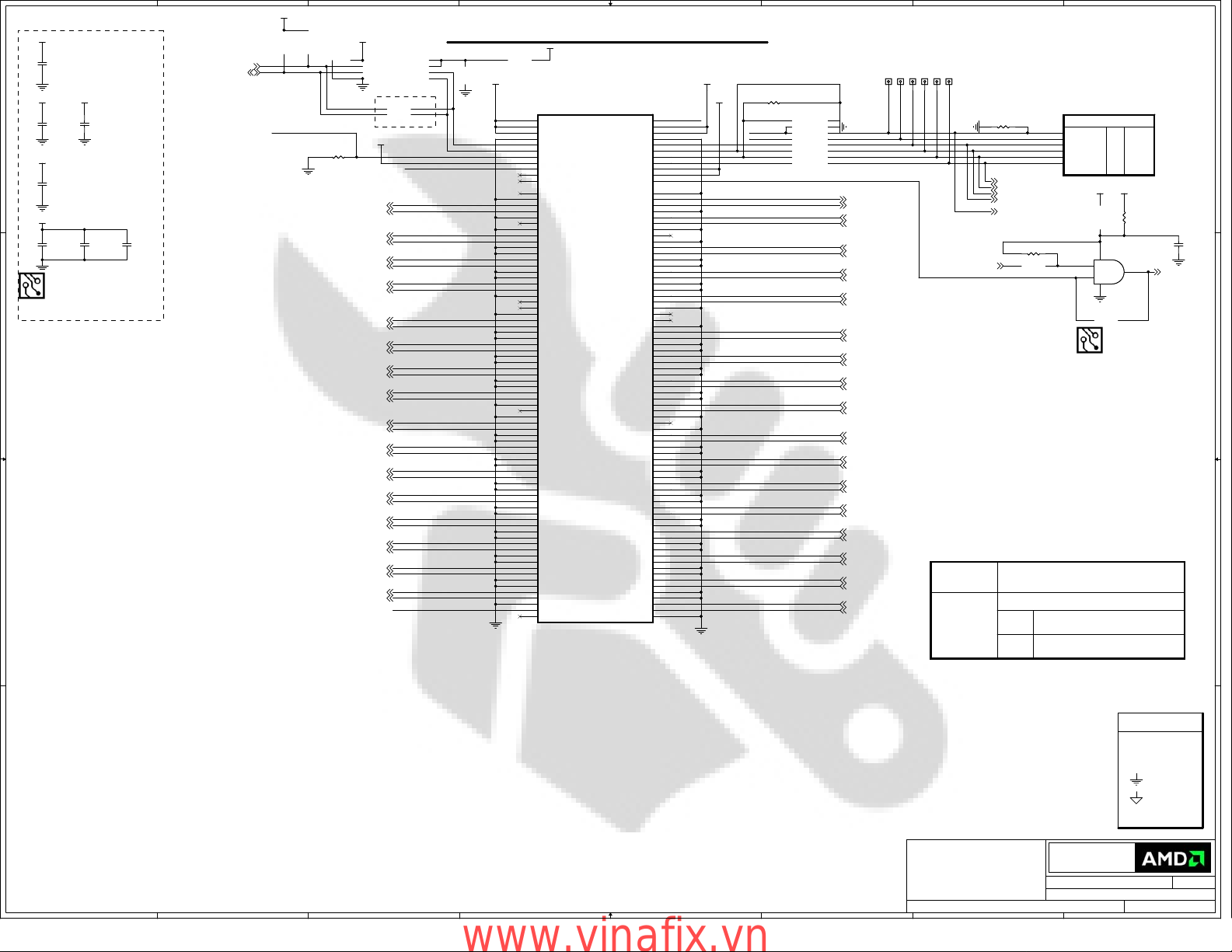
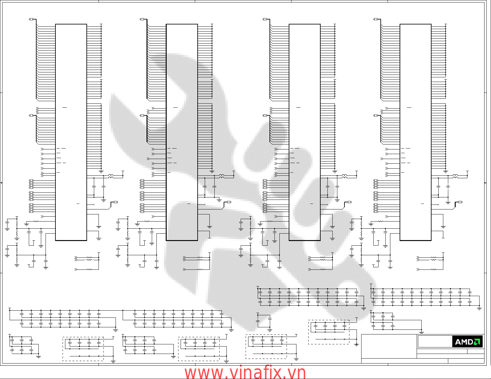
PCI-EXPRESS EDGE CONNECTOR
+12V_BUS
SMCLK
SMDAT
B1
B2
B3
B4
B5
B6
B7
B8
B9
B10
B11
B12
B13
B14
B15
B16
B17
B18
B19
B20
B21
B22
B23
B24
B25
B26
B27
B28
B29
B30
B31
B32
B33
B34
B35
B36
B37
B38
B39
B40
B41
B42
B43
B44
B45
B46
B47
B48
B49
B50
B51
B52
B53
B54
B55
B56
B57
B58
B59
B60
B61
B62
B63
B64
B65
B66
B67
B68
B69
B70
B71
B72
B73
B74
B75
B76
B77
B78
B79
B80
B81
B82
+3.3V
+12V#B1
+12V#B2
+12V#B3
GND#B4
SMCLK
SMDAT
GND#B7
+3.3V#B8
JTAG1
3.3Vaux
WAKE#
RSVD#B12
GND#B13
PETp0
PETn0
GND#B16
PRSNT2#B17
GND#B18
PETp1
PETn1
GND#B21
GND#B22
PETp2
PETn2
GND#B25
GND#B26
PETp3
PETn3
GND#B29
RSVD#B30
PRSNT2#B31
GND#B32
PETp4
PETn4
GND#B35
GND#B36
PETp5
PETn5
GND#B39
GND#B40
PETp6
PETn6
GND#B43
GND#B44
PETp7
PETn7
GND#B47
PRSNT2#B48
GND#B49
PETp8
PETn8
GND#B52
GND#B53
PETp9
PETn9
GND#B56
GND#B57
PETp10
PETn10
GND#B60
GND#B61
PETp11
PETn11
GND#B64
GND#B65
PETp12
PETn12
GND#B68
GND#B69
PETp13
PETn13
GND#B72
GND#B73
PETp14
PETn14
GND#B76
GND#B77
PETp15
PETn15
GND#B80
PRSNT2#B81
RSVD#B82
x16 PCIe
x16 PCIe
Mechanical Key
Mechanical Key
MPCIE1
MPCIE1
PRSNT1#A1
+12V#A2
+12V#A3
GND#A4
JTAG2
JTAG3
JTAG4
JTAG5
+3.3V#A9
+3.3V#A10
PERST#
GND#A12
REFCLK+
REFCLKGND#A15
PERp0
PERn0
GND#A18
RSVD#A19
GND#A20
PERp1
PERn1
GND#A23
GND#A24
PERp2
PERn2
GND#A27
GND#A28
PERp3
PERn3
GND#A31
RSVD#A32
RSVD#A33
GND#A34
PERp4
PERn4
GND#A37
GND#A38
PERp5
PERn5
GND#A41
GND#A42
PERp6
PERn6
GND#A45
GND#A46
PERp7
PERn7
GND#A49
RSVD#A50
GND#A51
PERp8
PERn8
GND#A54
GND#A55
PERp9
PERn9
GND#A58
GND#A59
PERp10
PERn10
GND#A62
GND#A63
PERp11
PERn11
GND#A66
GND#A67
PERp12
PERn12
GND#A70
GND#A71
PERp13
PERn13
GND#A74
GND#A75
PERp14
PERn14
GND#A78
GND#A79
PERp15
PERn15
GND#A82
A1
A2
A3
A4
A5
A6
A7
A8
A9
A10
A11
A12
A13
A14
A15
A16
A17
A18
A19
A20
A21
A22
A23
A24
A25
A26
A27
A28
A29
A30
A31
A32
A33
A34
A35
A36
A37
A38
A39
A40
A41
A42
A43
A44
A45
A46
A47
A48
A49
A50
A51
A52
A53
A54
A55
A56
A57
A58
A59
A60
A61
A62
A63
A64
A65
A66
A67
A68
A69
A70
A71
A72
A73
A74
A75
A76
A77
A78
A79
A80
A81
A82
4
PRESENCE
JTDI
+12V_BUS
+3.3V_BUS
PERp0
PERn0
PERp1
PERn1
PERp2
PERn2
PERp3
PERn3
PERp4
PERn4
PERp5
PERn5
PERp6
PERn6
PERp7
PERn7
PERp8
PERn8
PERp9
PERn9
PERp10
PERn10
PERp11
PERn11
PERp12
PERn12
PERp13
PERn13
PERp14
PERn14
PERp15
PERn15
JTCK
JTDO
JTMS
PERST#
JTRST
No JTAG
R2 0RR2 0R
3
JTAG_MODE
JTAG_TRSTB
JTAG_TCK
JTAG_TDI
JTAG_TDO
JTAG_TMS
PCIE_REFCLKP (2)
PCIE_REFCLKN (2)PETp0_GFXRp0(2)
PERp0 (2)
PERn0 (2)
PERp1 (2)
PERn1 (2)
PERp2 (2)
PERn2 (2)
PERp3 (2)
PERn3 (2)
PERp4 (2)
PERn4 (2)
PERp5 (2)
PERn5 (2)
PERp6 (2)
PERn6 (2)
PERp7 (2)
PERn7 (2)
PERp8 (2)
PERn8 (2)
PERp9 (2)
PERn9 (2)
PERp10 (2)
PERn10 (2)
PERp11 (2)
PERn11 (2)
PERp12 (2)
PERn12 (2)
PERp13 (2)
PERn13 (2)
PERp14 (2)
PERn14 (2)
PERp15 (2)
PERn15 (2)
TP4
TP4
35mil
35mil
TP1
TP1
TP32
TP32
TP2
TP2
TP5
TP5
TP3
TP3
35mil
35mil
35mil
35mil
35mil
35mil
35mil
35mil
35mil
35mil
PWR_GOOD(6,14,15,16)
Table 1: Connection for JTAG
Production
(No JTAG)
Internal Use Only
2
U1A
R21 1KR21 1K
JTAG_TMS (17)
JTAG_TDO (17)
JTAG_TCK (17)
JTAG_MODE (17)
JTAG_TDI (17)
MR9 1KMR9 1K
U1A
AD28
TESTEN
AM23
JTAG_TRSTB
AK23
JTAG_TCK
AN23
JTAG_TDI
AM24
JTAG_TDO
AL24
JTAG_TMS
RV730XT A12 HF MVE SLT B1
RV730XT A12 HF MVE SLT B1
Share one pad
Install R1, R2 & Don't Install TSW1
Install TSW1 & Don't Install R1 & R2
TSW1 Switch #1, 2, 3, 4, 5 and 6 closed (ON)
JTAG
#8 and 7 open
TSW1 Switch #1, 2, 3, 4, 5 and 6 open
NO JTAG
#8 & 7 closed (ON)
PART 1 OF 15
PART 1 OF 15
1
2
53
R_RST
1
J
J
T
T
A
A
G
G
+3.3V+3.3V_BUS
MR100RMR10
0R
Share one pad
NC7SZ08P5X_NL
NC7SZ08P5X_NL
4
U11
U11
DNI
Place R3 in U5
C4
100nF_6.3VC4100nF_6.3V
PERST#_buf (2,16)
TSW1, R1 & R2 are located on the bottom side of the board close to PCIE connector.
SYMBOL LEGEND
DO NOT
DNI
INSTALL
#
ACTIVE
LOW
DIGITAL
GROUND
ANALOG
A A
CONFIDENTIAL & PROPRIETARY TO ADVANCED MICRO DEVICES INC.
CONFIDENTIAL & PROPRIETARY TO ADVANCED MICRO DEVICES INC.
CONFIDENTIAL & PROPRIETARY TO ADVANCED MICRO DEVICES INC.
© 2007 Advanced Micro Devices
© 2007 Advanced Micro Devices
© 2007 Advanced Micro Devices
This AMD Board schematic and design is the exclusive property of AMD,
This AMD Board schematic and design is the exclusive property of AMD,
This AMD Board schematic and design is the exclusive property of AMD,
and is provided only to entities under a non-disclosure agreement
and is provided only to entities under a non-disclosure agreement
and is provided only to entities under a non-disclosure agreement
with AMD for evaluation purposes. Further distribution or disclosure
with AMD for evaluation purposes. Further distribution or disclosure
with AMD for evaluation purposes. Further distribution or disclosure
is strictly prohibited. Use of this schematic and design for any purpose
is strictly prohibited. Use of this schematic and design for any purpose
is strictly prohibited. Use of this schematic and design for any purpose
other than evaluation requires a Board Technology License Agreement
other than evaluation requires a Board Technology License Agreement
other than evaluation requires a Board Technology License Agreement
with AMD. AMD makes no representations or warranties of any kind
with AMD. AMD makes no representations or warranties of any kind
with AMD. AMD makes no representations or warranties of any kind
regarding this schematic and design, including, not limited to,
regarding this schematic and design, including, not limited to,
regarding this schematic and design, including, not limited to,
any implied warranty of merchantibility or fitness for a particular
any implied warranty of merchantibility or fitness for a particular
any implied warranty of merchantibility or fitness for a particular
purpose, and disclaims responsibility forany consequences resulting
purpose, and disclaims responsibility forany consequences resulting
purpose, and disclaims responsibility forany consequences resulting
from use of the information included herein.
from use of the information included herein.
from use of the information included herein.
Title
Title
8
7
6
5
4
3
Title
RH RV730 GDDR3 DVII-TVO-DVII
RH RV730 GDDR3 DVII-TVO-DVII
RH RV730 GDDR3 DVII-TVO-DVII
2
Advanced Micro Devices Inc.
Advanced Micro Devices Inc.
Advanced Micro Devices Inc.
1 Commerce Valley Drive East
1 Commerce Valley Drive East
1 Commerce Valley Drive East
Markham, Ontario
Markham, Ontario
Markham, Ontario
Tuesday, September 02, 2008
Tuesday, September 02, 2008
Tuesday, September 02, 2008
Sheet
Sheet
Sheet
of
119
of
119
of
119
GROUND
BUO BRING UP
ONLY
Doc No.
Doc No.
Doc No.
105-B709xx-11
105-B709xx-11
105-B709xx-11
1
RevDate:
RevDate:
RevDate:
50
50
50
www.vinafix.vn
Page 2
5
4
3
2
1
(2) RV730 PCIE Interface
NOTE: some of the PCIE testpoints will
be available trought via on traces.
PETp0_GFXRp0(1)
PETn0_GFXRn0(1)
PETp1_GFXRp1(1)
PETn1_GFXRn1(1)
D D
C C
+1.8V
+1.8V
+1.1V
B B
PETp2_GFXRp2(1)
PETn2_GFXRn2(1)
PETp3_GFXRp3(1)
PETn3_GFXRn3(1)
PETp4_GFXRp4(1)
PETn4_GFXRn4(1)
PETp5_GFXRp5(1)
PETn5_GFXRn5(1)
PETp6_GFXRp6(1)
PETn6_GFXRn6(1)
PETp7_GFXRp7(1)
PETn7_GFXRn7(1)
PETp8_GFXRp8(1)
PETn8_GFXRn8(1)
PETp9_GFXRp9(1)
PETn9_GFXRn9(1)
PETp10_GFXRp10(1)
PETn10_GFXRn10(1)
PETp11_GFXRp11(1)
PETn11_GFXRn11(1)
PETp12_GFXRp12(1)
PETn12_GFXRn12(1)
PETp13_GFXRp13(1)
PETn13_GFXRn13(1)
PETp14_GFXRp14(1)
PETn14_GFXRn14(1)
PETp15_GFXRp15(1)
PETn15_GFXRn15(1)
B22 BLM15BD121SN1B22 BLM15BD121SN1
B23 26R_600mAB23 26R_600mA
B21 220R_2AB21 220R_2A
+PCIE_PVDD
+PCIE_VDDR
+PCIE_VDDC
1uF_6.3V
1uF_6.3V
4.7uF_6.3V
4.7uF_6.3V
C101
C101
C94
C94
10uF_X6S
10uF_X6S
C98
C98
1uF_6.3V
1uF_6.3V
C95
C95
1uF_6.3V
1uF_6.3V
C90
C90
1uF_6.3V
1uF_6.3V
C51
C51
10uF_X6S
10uF_X6S
C86
C86
1uF_6.3V
1uF_6.3V
1uF_6.3V
1uF_6.3V
1uF_6.3V
1uF_6.3V
1uF_6.3V
1uF_6.3V
1uF_6.3V
1uF_6.3V
TP6TP6
TP13TP13
TP14TP14
TP7TP7
TP15TP15
TP8TP8
TP9TP9
TP16TP16
TP17TP17
TP10TP10
TP11TP11
TP18TP18
TP19TP19
TP12TP12
TP20TP20
TP21TP21
TP22TP22
TP23TP23
TP24TP24
TP25TP25
TP26TP26
TP27TP27
PCIE_REFCLKP(1)
PCIE_REFCLKN(1)
PERST#_buf(1,16)
C87
C87
C85
C85
C84
C100
C100
C92
C92
C89
C89
10nF
10nF
C97
C97
100nF_6.3V
100nF_6.3V
C93
C93
1uF_6.3V
1uF_6.3V
C84
100nF_6.3V
100nF_6.3V
C99
C99
100nF_6.3V
100nF_6.3V
C96
C96
C91
C91
1uF_6.3V
1uF_6.3V
C88
C88
1uF_6.3V
1uF_6.3V
U1B
U1B
AA38
PCIE_RX0P
Y37
PCIE_RX0N
Y35
PCIE_RX1P
W36
PCIE_RX1N
W38
PCIE_RX2P
V37
PCIE_RX2N
V35
PCIE_RX3P
U36
PCIE_RX3N
U38
PCIE_RX4P
T37
PCIE_RX4N
T35
PCIE_RX5P
R36
PCIE_RX5N
R38
PCIE_RX6P
P37
PCIE_RX6N
P35
PCIE_RX7P
N36
PCIE_RX7N
N38
PCIE_RX8P
M37
PCIE_RX8N
M35
PCIE_RX9P
L36
PCIE_RX9N
L38
PCIE_RX10P
K37
PCIE_RX10N
K35
PCIE_RX11P
J36
PCIE_RX11N
J38
PCIE_RX12P
H37
PCIE_RX12N
H35
PCIE_RX13P
G36
PCIE_RX13N
G38
PCIE_RX14P
F37
PCIE_RX14N
F35
PCIE_RX15P
E37
PCIE_RX15N
AB35
PCIE_REFCLKP
AA36
PCIE_REFCLKN
AA30
PERSTB
AB37
PCIE_PVDD
AA31
PCIE_VDDR#1
AA32
PCIE_VDDR#2
AA33
PCIE_VDDR#3
AA34
PCIE_VDDR#4
V28
PCIE_VDDR#5
W29
PCIE_VDDR#6
W30
PCIE_VDDR#7
Y31
PCIE_VDDR#8
G30
PCIE_VDDC#1
G31
PCIE_VDDC#2
H29
PCIE_VDDC#3
H30
PCIE_VDDC#4
J29
PCIE_VDDC#5
J30
PCIE_VDDC#6
L28
PCIE_VDDC#7
M28
PCIE_VDDC#8
N28
PCIE_VDDC#9
R28
PCIE_VDDC#10
T28
PCIE_VDDC#11
U28
PCIE_VDDC#12
RV730XT A12 HF MVE SLT B1
RV730XT A12 HF MVE SLT B1
PART 2 OF 15
PART 2 OF 15
P
P
C
C
I
I
E
E
X
X
P
P
R
R
E
E
S
S
S
S
PCIE_TX0P
PCIE_TX0N
PCIE_TX1P
PCIE_TX1N
PCIE_TX2P
PCIE_TX2N
PCIE_TX3P
PCIE_TX3N
PCIE_TX4P
PCIE_TX4N
PCIE_TX5P
PCIE_TX5N
PCIE_TX6P
PCIE_TX6N
PCIE_TX7P
PCIE_TX7N
PCIE_TX8P
PCIE_TX8N
PCIE_TX9P
PCIE_TX9N
PCIE_TX10P
PCIE_TX10N
PCIE_TX11P
PCIE_TX11N
PCIE_TX12P
PCIE_TX12N
PCIE_TX13P
PCIE_TX13N
PCIE_TX14P
PCIE_TX14N
PCIE_TX15P
PCIE_TX15N
PCIE_CALRP
PCIE_CALRN
PCIE_VSS#1
PCIE_VSS#2
PCIE_VSS#3
PCIE_VSS#4
PCIE_VSS#5
PCIE_VSS#6
PCIE_VSS#7
PCIE_VSS#8
PCIE_VSS#9
PCIE_VSS#10
PCIE_VSS#11
PCIE_VSS#12
PCIE_VSS#13
PCIE_VSS#14
PCIE_VSS#15
PCIE_VSS#16
PCIE_VSS#17
PCIE_VSS#18
PCIE_VSS#19
PCIE_VSS#20
PCIE_VSS#21
PCIE_VSS#22
PCIE_VSS#23
PCIE_VSS#24
PCIE_VSS#25
PCIE_VSS#26
PCIE_VSS#27
PCIE_VSS#28
PCIE_VSS#29
PCIE_VSS#30
PCIE_VSS#31
PCIE_VSS#32
PCIE_VSS#33
PCIE_VSS#34
PCIE_VSS#35
Y33
Y32
W33
W32
U33
U32
U30
U29
T33
T32
T30
T29
P33
P32
P30
P29
N33
N32
N30
N29
L33
L32
L30
L29
K33
K32
J33
J32
K30
K29
H33
H32
Y30
Y29
AB39
E39
F34
F39
G33
G34
H31
H34
H39
J31
J34
K31
K34
K39
L31
L34
M34
M39
N31
N34
P31
P34
P39
R34
T31
T34
T39
U31
U34
V34
V39
W31
W34
Y34
Y39
PCIE_TX0P
PCIE_TX0N
PCIE_TX1P
PCIE_TX1N
PCIE_TX2P
PCIE_TX2N
PCIE_TX3P
PCIE_TX3N
PCIE_TX4P
PCIE_TX4N
PCIE_TX5P
PCIE_TX5N
PCIE_TX6P
PCIE_TX6N
PCIE_TX7P
PCIE_TX7N
PCIE_TX8P
PCIE_TX8N
PCIE_TX9P
PCIE_TX9N
PCIE_TX10P
PCIE_TX10N
PCIE_TX11P
PCIE_TX11N
PCIE_TX12P
PCIE_TX12N
PCIE_TX13P
PCIE_TX13N
PCIE_TX14P
PCIE_TX14N
PCIE_TX15P
PCIE_TX15N
PCIE_CALRP
PCIE_CALRN
100nF_6.3V
100nF_6.3V
100nF_6.3V
100nF_6.3V
100nF_6.3V
100nF_6.3V
100nF_6.3V
100nF_6.3V
100nF_6.3V
100nF_6.3V
100nF_6.3V
100nF_6.3V
100nF_6.3V
100nF_6.3V
100nF_6.3V
100nF_6.3V
100nF_6.3V
100nF_6.3V
100nF_6.3V
100nF_6.3V
100nF_6.3V
100nF_6.3V
100nF_6.3V
100nF_6.3V
100nF_6.3V
100nF_6.3V
100nF_6.3V
100nF_6.3V
100nF_6.3V
100nF_6.3V
100nF_6.3V
100nF_6.3V
C11
C11
100nF_6.3V
100nF_6.3V
C13
C13
R221.27K R221.27K
R242.0K R242.0K
C12
C12
C14
C14
100nF_6.3V
100nF_6.3V
C15
C15
C16
C16
100nF_6.3V
100nF_6.3V
C17
C17
C18
C18
100nF_6.3V
100nF_6.3V
C19
C19
C20
C20
100nF_6.3V
100nF_6.3V
C21
C21
C22
C22
100nF_6.3V
100nF_6.3V
C23
C23
C24
C24
100nF_6.3V
100nF_6.3V
C25
C25
C26
C26
100nF_6.3V
100nF_6.3V
C27
C27
C28
C28
100nF_6.3V
100nF_6.3V
C29
C29
C30
C30
100nF_6.3V
100nF_6.3V
C31
C31
C32
C32
100nF_6.3V
100nF_6.3V
C33
C33
C34
C34
100nF_6.3V
100nF_6.3V
C35
C35
C36
C36
100nF_6.3V
100nF_6.3V
C37
C37
C38
C38
100nF_6.3V
100nF_6.3V
C39
C39
C40
C40
100nF_6.3V
100nF_6.3V
C41
C41
C42
C42
100nF_6.3V
100nF_6.3V
+PCIE_VDDC
PERp0 (1)
PERn0 (1)
PERp1 (1)
PERn1 (1)
PERp2 (1)
PERn2 (1)
PERp3 (1)
PERn3 (1)
PERp4 (1)
PERn4 (1)
PERp5 (1)
PERn5 (1)
PERp6 (1)
PERn6 (1)
PERp7 (1)
PERn7 (1)
PERp8 (1)
PERn8 (1)
PERp9 (1)
PERn9 (1)
PERp10 (1)
PERn10 (1)
PERp11 (1)
PERn11 (1)
PERp12 (1)
PERn12 (1)
PERp13 (1)
PERn13 (1)
PERp14 (1)
PERn14 (1)
PERp15 (1)
PERn15 (1)
A A
CONFIDENTIAL & PROPRIETARY TO ADVANCED MICRO DEVICES INC.
CONFIDENTIAL & PROPRIETARY TO ADVANCED MICRO DEVICES INC.
CONFIDENTIAL & PROPRIETARY TO ADVANCED MICRO DEVICES INC.
© 2007 Advanced Micro Devices
© 2007 Advanced Micro Devices
© 2007 Advanced Micro Devices
This AMD Board schematic and design is the exclusive property of AMD,
This AMD Board schematic and design is the exclusive property of AMD,
This AMD Board schematic and design is the exclusive property of AMD,
and is provided only to entities under a non-disclosure agreement
and is provided only to entities under a non-disclosure agreement
and is provided only to entities under a non-disclosure agreement
with AMD for evaluation purposes. Further distribution or disclosure
with AMD for evaluation purposes. Further distribution or disclosure
with AMD for evaluation purposes. Further distribution or disclosure
is strictly prohibited. Use of this schematic and design for any purpose
is strictly prohibited. Use of this schematic and design for any purpose
is strictly prohibited. Use of this schematic and design for any purpose
other than evaluation requires a Board Technology License Agreement
other than evaluation requires a Board Technology License Agreement
other than evaluation requires a Board Technology License Agreement
with AMD. AMD makes no representations or warranties of any kind
with AMD. AMD makes no representations or warranties of any kind
with AMD. AMD makes no representations or warranties of any kind
regarding this schematic and design, including, not limited to,
regarding this schematic and design, including, not limited to,
regarding this schematic and design, including, not limited to,
any implied warranty of merchantibility or fitness for a particular
any implied warranty of merchantibility or fitness for a particular
any implied warranty of merchantibility or fitness for a particular
purpose, and disclaims responsibility forany consequences resulting
purpose, and disclaims responsibility forany consequences resulting
purpose, and disclaims responsibility forany consequences resulting
from use of the information included herein.
from use of the information included herein.
from use of the information included herein.
Title
Title
5
4
3
2
Title
RH RV730 GDDR3 DVII-TVO-DVII
RH RV730 GDDR3 DVII-TVO-DVII
RH RV730 GDDR3 DVII-TVO-DVII
Advanced Micro Devices Inc.
Advanced Micro Devices Inc.
Advanced Micro Devices Inc.
1 Commerce Valley Drive East
1 Commerce Valley Drive East
1 Commerce Valley Drive East
Markham, Ontario
Markham, Ontario
Markham, Ontario
Tuesday, September 02, 2008
Tuesday, September 02, 2008
Tuesday, September 02, 2008
Sheet
Sheet
Sheet
of
219
of
219
of
219
1
Doc No.
Doc No.
Doc No.
RevDate:
RevDate:
RevDate:
50
50
50
105-B709xx-11
105-B709xx-11
105-B709xx-11
www.vinafix.vn
Page 3
5
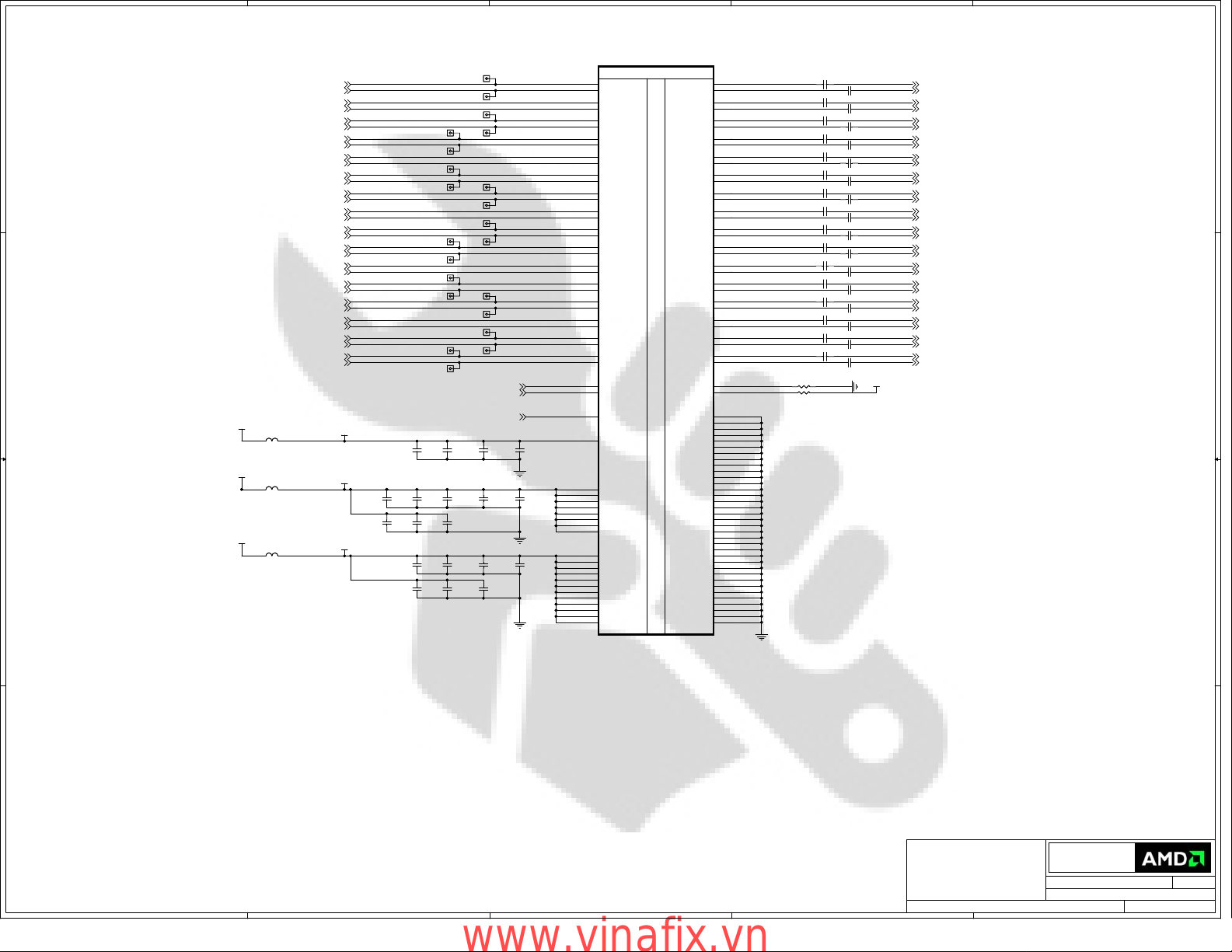
(3) RV730 MEM Interface Ch A&B
DQA0_0
DQA0_1
DQA0_2
DQA0_3
DQA0_4
DQA0_5
DQA0_6
DQA0_7
DQA0_8
DQA0_9
DQA0_10
D D
DQMA_0(4,5)
DQMA_1(4,5)
DQMA_2(4,5)
DQMA_3(4,5)
QSA_0(4,5)
QSA_1(4,5)
QSA_2(4,5)
QSA_3(4,5)
QSA_0b(4,5)
QSA_1b(4,5)
QSA_2b(4,5)
QSA_3b(4,5)
C C
MAA_[12..0](4,5)
B B
MAA_BA_[2..0](4,5)
DRAM_RST(4,5)
DQA0_11
DQA0_12
DQA0_13
DQA0_14
DQA0_15
DQA0_16
DQA0_17
DQA0_18
DQA0_19
DQA0_20
DQA0_21
DQA0_22
DQA0_23
DQA0_24
DQA0_25
DQA0_26
DQA0_27
DQA0_28
DQA0_29
DQA0_30
DQA0_31
CKEA0(4,5)
CLKA0(4,5)
CLKA0b(4,5)
CSA0b_0(4)
CSA0b_1(5) CSB0b_1(5)CSA1b_1 (5) CSB1b_1 (5)
CASA0b(4,5)
RASA0b(4,5)
WEA0b(4,5)
MAA_0
MAA_1
MAA_2
MAA_3
MAA_4
MAA_5
MAA_6
MAA_7
MAA_8
MAA_9
MAA_10
MAA_11
MAA_12
MAA_BA_0
MAA_BA_1
MAA_BA_2
C346
C346
1uF_6.3V
1uF_6.3V
R102
R102
10K
10K
AH11
C37
C35
A35
E34
G32
D33
F32
E32
D31
F30
C30
A30
F28
C28
A28
E28
D27
F26
C26
A26
F24
C24
A24
E24
C22
A22
F22
D21
A20
F20
D19
E18
A32
C32
D23
E22
C34
D29
D25
E20
A34
E30
E26
C20
J21
K21
H27
G27
K24
K27
K20
K23
K26
G24
J23
H24
J24
H26
J26
H21
G21
H19
H20
L13
G16
J16
H23
J19
J17
H17
H16
U1C
U1C
DQA_0
DQA_1
DQA_2
DQA_3
DQA_4
DQA_5
DQA_6
DQA_7
DQA_8
DQA_9
DQA_10
DQA_11
DQA_12
DQA_13
DQA_14
DQA_15
DQA_16
DQA_17
DQA_18
DQA_19
DQA_20
DQA_21
DQA_22
DQA_23
DQA_24
DQA_25
DQA_26
DQA_27
DQA_28
DQA_29
DQA_30
DQA_31
DQMA_0
DQMA_1
DQMA_2
DQMA_3
QSA_0
QSA_1
QSA_2
QSA_3
QSA_0B
QSA_1B
QSA_2B
QSA_3B
ODTA0
CKEA0
CLKA0
CLKA0B
CSA0B_0
CSA0B_1
CASA0B
RASA0B
WEA0B
MAA_0
MAA_1
MAA_2
MAA_3
MAA_4
MAA_5
MAA_6
MAA_7
MAA_8
MAA_9
MAA_10
MAA_11
MAA_12
NC_MAA_13
NC_MAA_14
MAA_BA0
MAA_BA1
MAA_BA2
DRAM_RST
RV730XT A12 HF MVE SLT B1
RV730XT A12 HF MVE SLT B1
DDR2
DDR2
Single or
Single or
PART 3 OF 15
PART 3 OF 15
Diff Strobes
Diff Strobes
DDR3
DDR3
M
M
E
E
M
M
O
O
R
R
Y
Y
I
I
N
N
T
T
E
E
R
R
F
F
A
A
C
C
E
E
Differential Strobes
Differential Strobes
B
B
A
A
N
N
K
K
A
A
DQA_32
DQA_33
DQA_34
DQA_35
DQA_36
DQA_37
DQA_38
DQA_39
DQA_40
DQA_41
DQA_42
DQA_43
DQA_44
DQA_45
DQA_46
DQA_47
DQA_48
DQA_49
DQA_50
DQA_51
DQA_52
DQA_53
DQA_54
DQA_55
DQA_56
DQA_57
DQA_58
DQA_59
DQA_60
DQA_61
DQA_62
DQA_63
DQMA_4
DQMA_5
DQMA_6
DQMA_7
GDDR3
GDDR3
Read
Strobes
Read
Strobes
QSA_4B
QSA_5B
QSA_6B
QSA_7B
Write
Strobes
Write
Strobes
CLKA1B
CSA1B_0
CSA1B_1
CASA1B
RASA1B
NC_MEM_CALRP0
NC_MEM_CALRN0
MEM_CALRP1
NC_MEM_CALRN1
NC_MEM_CALRP2
NC_MEM_CALRN2
MVREFDA
MVREFSA
C18
A18
F18
D17
A16
F16
D15
E14
F14
D13
F12
A12
D11
F10
A10
C10
G13
H13
J13
H11
G10
G8
K9
K10
G9
A8
C8
E8
A6
C6
E6
A5
C14
A14
E10
D9
E16
QSA_4
E12
QSA_5
J10
QSA_6
D7
QSA_7
C16
C12
J11
F8
G19
ODTA1
J20
CKEA1
J14
CLKA1
H14
M13
K16
K17
K19
L15
WEA1B
M27
L27
M12
N12
AH12
AG12
L18
MVREFD/S =0.7*
VDDR1
(GDDR3/4/5)
L20
DQA1_0
DQA1_1
DQA1_2
DQA1_3
DQA1_4
DQA1_5
DQA1_6
DQA1_7
DQA1_8
DQA1_9
DQA1_10
DQA1_11
DQA1_12
DQA1_13
DQA1_14
DQA1_15
DQA1_16
DQA1_17
DQA1_18
DQA1_19
DQA1_20
DQA1_21
DQA1_22
DQA1_23
DQA1_24
DQA1_25
DQA1_26
DQA1_27
DQA1_28
DQA1_29
DQA1_30
DQA1_31
MEM_CALRP0
MEM_CALRN0
MEM_CALRP1
MEM_CALRN1
MEM_CALRP2
MEM_CALRN2
MVREFD_A
MVREFS_A
4
3
U1D
DQA1_[31..0] (4,5)DQA0_[31..0](4,5) DQB0_[31..0](4,5) DQB1_[31..0] (4,5)
CKEA1 (4,5)
CLKA1 (4,5)
CLKA1b (4,5)
CSA1b_0 (4)
CASA1b (4,5)
RASA1b (4,5)
WEA1b (4,5)
R118 243RR118 243R
DNI
1uF_6.3V
1uF_6.3V
DNI
1uF_6.3V
1uF_6.3V
DQMA_4 (4,5)
DQMA_5 (4,5)
DQMA_6 (4,5)
DQMA_7 (4,5)
QSA_4 (4,5)
QSA_5 (4,5)
QSA_6 (4,5)
QSA_7 (4,5)
QSA_4b (4,5)
QSA_5b (4,5)
QSA_6b (4,5)
QSA_7b (4,5)
R122
R122
40.2R
40.2R
1%
R125
R125
C300
C300
100R
100R
1%
R126
R126
40.2R
40.2R
R128
R128
C305
C305
100R
100R
1%
+MVDD
+MVDD
+MVDD
DQMB_0(4,5)
DQMB_1(4,5)
DQMB_2(4,5)
DQMB_3(4,5)
QSB_0(4,5)
QSB_1(4,5)
QSB_2(4,5)
QSB_3(4,5)
QSB_0b(4,5)
QSB_1b(4,5)
QSB_2b(4,5)
QSB_3b(4,5)
MAB_[12..0](4,5)
MAB_BA_[2..0](4,5)
DQB0_0
DQB0_1
DQB0_2
DQB0_3
DQB0_4
DQB0_5
DQB0_6
DQB0_7
DQB0_8
DQB0_9
DQB0_10
DQB0_11
DQB0_12
DQB0_13
DQB0_14
DQB0_15
DQB0_16
DQB0_17
DQB0_18
DQB0_19
DQB0_20
DQB0_21
DQB0_22
DQB0_23
DQB0_24
DQB0_25
DQB0_26
DQB0_27
DQB0_28
DQB0_29
DQB0_30
DQB0_31
CKEB0(4,5)
CLKB0(4,5)
CLKB0b(4,5)
CSB0b_0(4)
CASB0b(4,5)
RASB0b(4,5)
WEB0b(4,5)
MAB_0
MAB_1
MAB_2
MAB_3
MAB_4
MAB_5
MAB_6
MAB_7
MAB_8
MAB_9
MAB_10
MAB_11
MAB_12
MAB_BA_0
MAB_BA_1
MAB_BA_2
U1D
C5
DQB_0
C3
DQB_1
E3
DQB_2
E1
DQB_3
F1
DQB_4
F3
DQB_5
F5
DQB_6
G4
DQB_7
H5
DQB_8
H6
DQB_9
J4
DQB_10
K6
DQB_11
K5
DQB_12
L4
DQB_13
M6
DQB_14
M1
DQB_15
M3
DQB_16
M5
DQB_17
N4
DQB_18
P6
DQB_19
P5
DQB_20
R4
DQB_21
T6
DQB_22
T1
DQB_23
U4
DQB_24
V6
DQB_25
V1
DQB_26
V3
DQB_27
Y6
DQB_28
Y1
DQB_29
Y3
DQB_30
Y5
DQB_31
H3
DQMB_0
H1
DQMB_1
T3
DQMB_2
T5
DQMB_3
F6
QSB_0
K3
QSB_1
P3
QSB_2
V5
QSB_3
G7
QSB_0B
K1
QSB_1B
P1
QSB_2B
W4
QSB_3B
T7
ODTB0
U10
CKEB0
L9
CLKB0
L8
CLKB0B
P10
CSB0B_0
L10
CSB0B_1
W10
CASB0B
T10
RASB0B
N10
WEB0B
P8
MAB_0
T9
MAB_1
P9
MAB_2
N7
MAB_3
N8
MAB_4
N9
MAB_5
U9
MAB_6
U8
MAB_7
Y9
MAB_8
W9
MAB_9
AC8
MAB_10
AC9
MAB_11
AA7
MAB_12
T8
NC_MAB_13
W8
NC_MAB_14
Y8
MAB_BA0
AA9
MAB_BA1
AA8
MAB_BA2
RV730XT A12 HF MVE SLT B1
RV730XT A12 HF MVE SLT B1
DDR2
DDR2
Single or
Diff Strobes
Single or
Diff Strobes
PART 4 OF 15
PART 4 OF 15
M
M
E
E
M
M
O
O
R
R
Y
Y
I
I
N
N
T
T
E
E
R
R
F
F
A
A
C
C
E
E
DDR3 GDDR3
DDR3 GDDR3
Differential Strobes
Differential Strobes
B
B
A
A
N
N
K
K
B
B
2
DQB1_0
AA4
DQB_32
DQB_33
DQB_34
DQB_35
DQB_36
DQB_37
DQB_38
DQB_39
DQB_40
DQB_41
DQB_42
DQB_43
DQB_44
DQB_45
DQB_46
DQB_47
DQB_48
DQB_49
DQB_50
DQB_51
DQB_52
DQB_53
DQB_54
DQB_55
DQB_56
DQB_57
DQB_58
DQB_59
DQB_60
DQB_61
DQB_62
DQB_63
DQMB_4
DQMB_5
DQMB_6
DQMB_7
QSB_4
QSB_5
QSB_6
QSB_7
Read
Strobes
Read
Strobes
QSB_4B
QSB_5B
QSB_6B
QSB_7B
Write
Strobes
Write
Strobes
ODTB1
CKEB1
CLKB1
CLKB1B
CSB1B_0
CSB1B_1
CASB1B
RASB1B
WEB1B
MVREFDB
MVREFSB
DQB1_1
AB6
DQB1_2
AB1
DQB1_3
AB3
DQB1_4
AD6
DQB1_5
AD1
DQB1_6
AD3
DQB1_7
AD5
DQB1_8
AF1
DQB1_9
AF3
DQB1_10
AF6
DQB1_11
AG4
DQB1_12
AH5
DQB1_13
AH6
DQB1_14
AJ4
DQB1_15
AK3
DQB1_16
AF8
DQB1_17
AF9
DQB1_18
AG8
DQB1_19
AG7
DQB1_20
AK9
DQB1_21
AL7
DQB1_22
AM8
DQB1_23
AM7
DQB1_24
AK1
DQB1_25
AL4
DQB1_26
AM6
DQB1_27
AM1
DQB1_28
AN4
DQB1_29
AP3
DQB1_30
AP1
DQB1_31
AP5
AE4
AF5
AK6
AK5
AB5
AH1
AJ9
AM5
AC4
AH3
AJ8
AM3
W7
AA11
AD8
AD7
AD10
AC10
AA10
Y10
AB11
MVREFD_B
Y12
MVREFD/S =0.7*
VDDR1
(GDDR3/4/5)
MVREFS_B
AA12
CKEB1 (4,5)
CLKB1 (4,5)
CLKB1b (4,5)
CSB1b_0 (4)
CASB1b (4,5)
RASB1b (4,5)
WEB1b (4,5)
DNI
C298
C298
1uF_6.3V
1uF_6.3V
DNI
C307
C307
1uF_6.3V
1uF_6.3V
DQMB_4 (4,5)
DQMB_5 (4,5)
DQMB_6 (4,5)
DQMB_7 (4,5)
QSB_4 (4,5)
QSB_5 (4,5)
QSB_6 (4,5)
QSB_7 (4,5)
QSB_4b (4,5)
QSB_5b (4,5)
QSB_6b (4,5)
QSB_7b (4,5)
R123
R123
40.2R
40.2R
1%
R124
R124
100R
100R
1%
R127
R127
40.2R
40.2R
1%1%
R129
R129
100R
100R
1%
1
+MVDD
+MVDD
A A
CONFIDENTIAL & PROPRIETARY TO ADVANCED MICRO DEVICES INC.
CONFIDENTIAL & PROPRIETARY TO ADVANCED MICRO DEVICES INC.
CONFIDENTIAL & PROPRIETARY TO ADVANCED MICRO DEVICES INC.
© 2007 Advanced Micro Devices
© 2007 Advanced Micro Devices
© 2007 Advanced Micro Devices
This AMD Board schematic and design is the exclusive property of AMD,
This AMD Board schematic and design is the exclusive property of AMD,
This AMD Board schematic and design is the exclusive property of AMD,
and is provided only to entities under a non-disclosure agreement
and is provided only to entities under a non-disclosure agreement
and is provided only to entities under a non-disclosure agreement
with AMD for evaluation purposes. Further distribution or disclosure
with AMD for evaluation purposes. Further distribution or disclosure
with AMD for evaluation purposes. Further distribution or disclosure
is strictly prohibited. Use of this schematic and design for any purpose
is strictly prohibited. Use of this schematic and design for any purpose
is strictly prohibited. Use of this schematic and design for any purpose
other than evaluation requires a Board Technology License Agreement
other than evaluation requires a Board Technology License Agreement
other than evaluation requires a Board Technology License Agreement
with AMD. AMD makes no representations or warranties of any kind
with AMD. AMD makes no representations or warranties of any kind
with AMD. AMD makes no representations or warranties of any kind
regarding this schematic and design, including, not limited to,
regarding this schematic and design, including, not limited to,
regarding this schematic and design, including, not limited to,
any implied warranty of merchantibility or fitness for a particular
any implied warranty of merchantibility or fitness for a particular
any implied warranty of merchantibility or fitness for a particular
purpose, and disclaims responsibility forany consequences resulting
purpose, and disclaims responsibility forany consequences resulting
purpose, and disclaims responsibility forany consequences resulting
from use of the information included herein.
from use of the information included herein.
from use of the information included herein.
Title
Title
5
4
3
2
Title
RH RV730 GDDR3 DVII-TVO-DVII
RH RV730 GDDR3 DVII-TVO-DVII
RH RV730 GDDR3 DVII-TVO-DVII
Advanced Micro Devices Inc.
Advanced Micro Devices Inc.
Advanced Micro Devices Inc.
1 Commerce Valley Drive East
1 Commerce Valley Drive East
1 Commerce Valley Drive East
Markham, Ontario
Markham, Ontario
Markham, Ontario
Tuesday, September 02, 2008
Tuesday, September 02, 2008
Tuesday, September 02, 2008
Sheet
Sheet
Sheet
of
319
of
319
of
319
1
Doc No.
Doc No.
Doc No.
RevDate:
RevDate:
RevDate:
50
50
50
105-B709xx-11
105-B709xx-11
105-B709xx-11
www.vinafix.vn
Page 4
5
4
3
2
1
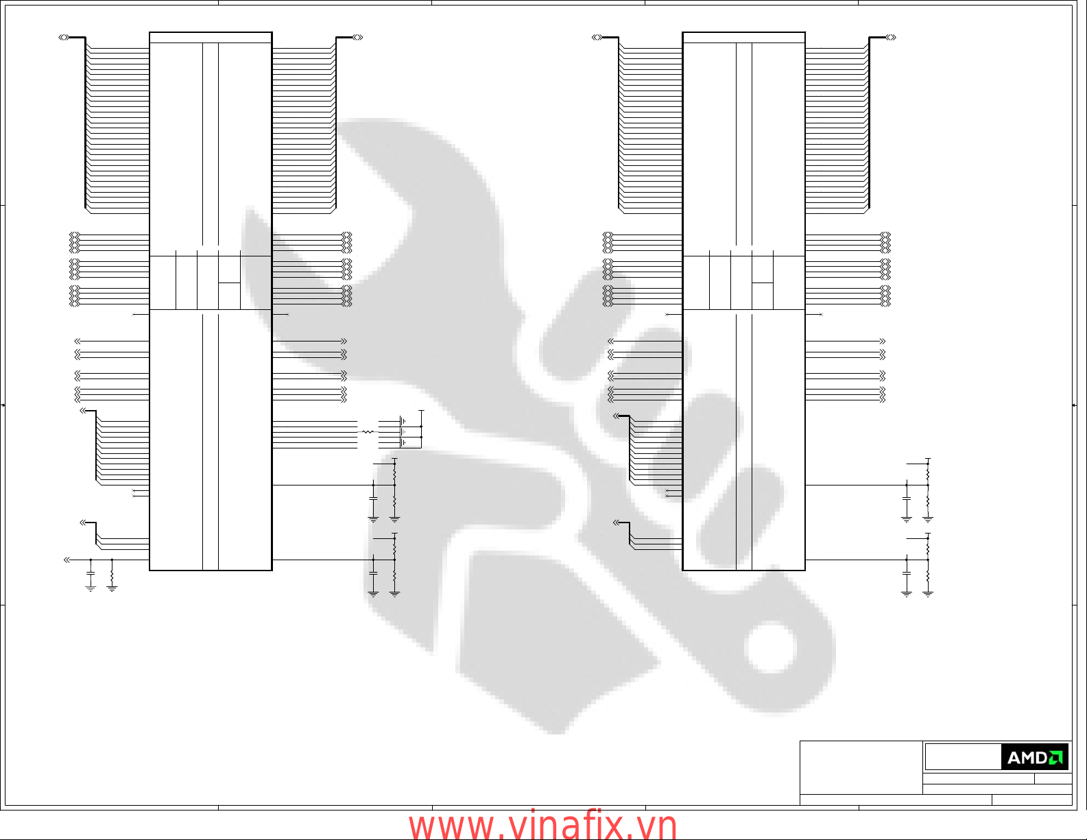
(4) GDDR3 Memory Channel A&B Bank 0
DQA0_[31..0](3,5)
D D
RASA0b(3,5)
MAA_BA_0(3,5)
MAA_BA_1(3,5)
MAA_[12..0](3,5)
C C
CASA0b(3,5)
CKEA0(3,5)
MAA_BA_2(3,5)
CSA0b_0(3)
WEA0b(3,5)
CLKA0b(3,5)
CLKA0(3,5)
QSA_0
QSA_0(3,5)
QSA_1
QSA_1(3,5)
QSA_3
QSA_3(3,5)
QSA_2
QSA_2(3,5)
QSA_0b
QSA_0b(3,5)
QSA_1b
QSA_1b(3,5)
QSA_3b
QSA_3b(3,5)
QSA_2b
QSA_2b(3,5)
DQMA_0
DQMA_0(3,5)
DQMA_1
DQMA_1(3,5)
DQMA_3
DQMA_3(3,5)
DQMA_2
DQMA_2(3,5)
+MVDD
DRAM_RST(3,5)
R219
R219
C244
C244
2.37K
2.37K
10nF
10nF
B B
A A
+MVDD
+MVDD
+MVDD
C245
C245
10nF
10nF
C2201
C2201
100nF_6.3V
100nF_6.3V
C2212
C2212
1uF_6.3V
1uF_6.3V
C223
C223
100nF_6.3V
100nF_6.3V
C228
C228
1uF_6.3V
1uF_6.3V
R220
R220
5.49K
5.49K
R221
R221
2.37K
2.37K
R222
R222
5.49K
5.49K
+MVDD
C2202
C2202
100nF_6.3V
100nF_6.3V
C2213
C2213
1uF_6.3V
1uF_6.3V
C224
C224
100nF_6.3V
100nF_6.3V
C229
C229
1uF_6.3V
1uF_6.3V
C238
C238
100nF_6.3V
100nF_6.3V
+MVDD
C240
C240
100nF_6.3V
100nF_6.3V
C2203
C2203
100nF_6.3V
100nF_6.3V
C2214
C2214
1uF_6.3V
1uF_6.3V
C225
C225
100nF_6.3V
100nF_6.3V
C230
C230
1uF_6.3V
1uF_6.3V
DQA0_0
DQA0_2
DQA0_1
DQA0_4
DQA0_5
DQA0_3
DQA0_7
DQA0_6
DQA0_10
DQA0_11
DQA0_12
DQA0_14
DQA0_15
DQA0_9
DQA0_13
DQA0_8
DQA0_27
DQA0_26
DQA0_24
DQA0_25
DQA0_28
DQA0_30
DQA0_31
DQA0_29
DQA0_16
DQA0_17
DQA0_19
DQA0_18
DQA0_21
DQA0_22
DQA0_20
DQA0_23
MAA_7
MAA_8
MAA_3
MAA_10
MAA_11
MAA_2
MAA_1
MAA_0
MAA_9
MAA_6
MAA_5
MAA_4
R218
R218
243R
243R
C239
C239
10nF
10nF
C2205
C2205
100nF_6.3V
100nF_6.3V
C216
C216
1uF_6.3V
1uF_6.3V
C226
C226
100nF_6.3V
100nF_6.3V
C231
C231
1uF_6.3V
1uF_6.3V
C241
C241
10nF
10nF
T3
T2
R3
R2
M3
N2
L3
M2
T10
T11
R10
R11
M10
N11
L10
M11
G10
F11
F10
E11
C10
C11
B10
B11
G3
F2
F3
E2
C3
C2
B3
B2
H10
G9
G4
L4
K2
M9
K11
L9
K10
H11
K9
M4
K3
H2
K4
F9
H9
H3
F4
H4
J10
J11
P3
P10
D10
D3
P2
P11
D11
D2
N3
N10
E10
E3
V9
A4
H1
H12
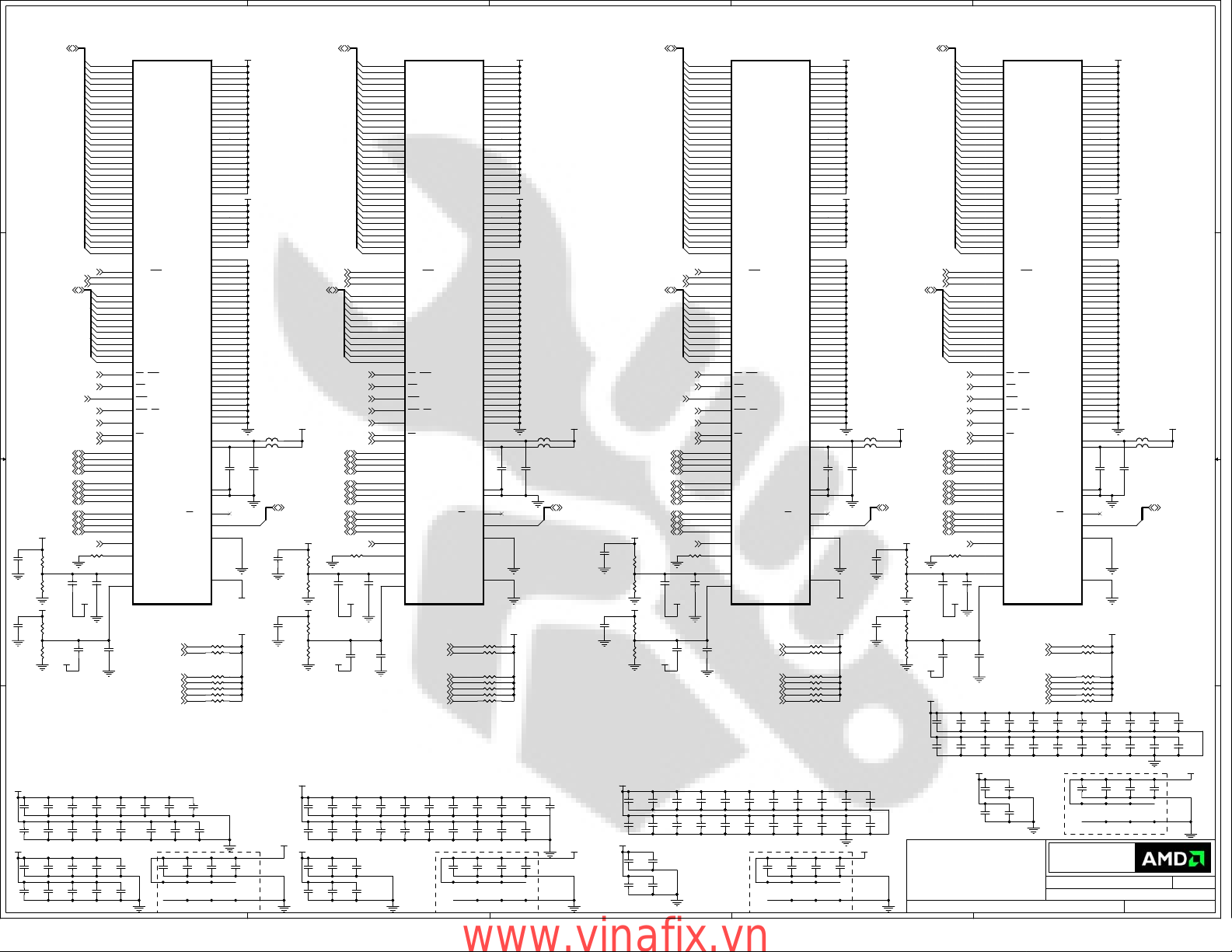
U201
U201
DQ31 | DQ23
DQ30 | DQ22
DQ29 | DQ21
DQ28 | DQ20
DQ27 | DQ19
DQ26 | DQ18
DQ25 | DQ17
DQ24 | DQ16
DQ23 | DQ31
DQ22 | DQ30
DQ21 | DQ29
DQ20 | DQ28
DQ19 | DQ27
DQ18 | DQ26
DQ17 | DQ25
DQ16 | DQ24
DQ15 | DQ7
DQ14 | DQ6
DQ13 | DQ5
DQ12 | DQ4
DQ11 | DQ3
DQ10 | DQ2
DQ9 | DQ1
DQ8 | DQ0
DQ7 | DQ15
DQ6 | DQ14
DQ5 | DQ13
DQ4 | DQ12
DQ3 | DQ11
DQ2 | DQ10
DQ1 | DQ9
DQ0 | DQ8
BA2 | RAS
BA1 | BA0
BA0 | BA1
A11 | A7
A10 | A8
A9 | A3
A8/AP | A10
A7 | A11
A6 | A2
A5 | A1
A4 | A0
A3 | A9
A2 | A6
A1 | A5
A0 | A4
CS | CAS
WE | CKE
RAS | BA2
CAS | CS
CKE | WE
CK
CK
RDQS3 | RDQS2
RDQS2 | RDQS3
RDQS1 | RDQS0
RDQS0 | RDQS1
WDQS3 | WDQS2
WDQS2 | WDQS3
WDQS1 | WDQS0
WDQS0 | WDQS1
DM3 | DM2
DM2 | DM3
DM1 | DM0
DM0 | DM1
RESET
ZQ
VREF
VREF#H12
23C21287QT1A
23C21287QT1A
C2207
C2207
100nF_6.3V
100nF_6.3V
C218
C218
1uF_6.3V
1uF_6.3V
C227
C227
100nF_6.3V
100nF_6.3V
C232
C232
1uF_6.3V
1uF_6.3V
5
CLKA0(3,5)
CLKA0b(3,5)
CKEA0(3,5)
RASA0b(3,5)
CASA0b(3,5)
WEA0b(3,5)
CSA0b_0(3)
C209
C209
100nF_6.3V
100nF_6.3V
C220
C220
1uF_6.3V
1uF_6.3V
VDDQ
VDDQ#A12
VDDQ#C1
VDDQ#C4
VDDQ#C9
VDDQ#C12
VDDQ#E1
VDDQ#E4
VDDQ#E9
VDDQ#E12
VDDQ#J4
VDDQ#J9
VDDQ#N1
VDDQ#N4
VDDQ#N9
VDDQ#N12
VDDQ#R1
VDDQ#R4
VDDQ#R9
VDDQ#R12
VDDQ#V1
VDDQ#V12
VDD#A11
VDD#F1
VDD#F12
VDD#M1
VDD#M12
VDD#V2
VDD#V11
VSSQ#B4
VSSQ#B9
VSSQ#B12
VSSQ#D1
VSSQ#D4
VSSQ#D9
VSSQ#D12
VSSQ#G2
VSSQ#G11
VSSQ#L2
VSSQ#L11
VSSQ#P1
VSSQ#P4
VSSQ#P9
VSSQ#P12
VSSQ#T1
VSSQ#T4
VSSQ#T9
VSSQ#T12
VSS#A10
VSS#G1
VSS#G12
VSS#L1
VSS#L12
VSS#V3
VSS#V10
VDDA#K12
VSSA#J12
RAR/CS1/RFU2
A12/RAR/RFU1
GND | VDD
GND | VDD
C2210
C2210
100nF_6.3V
100nF_6.3V
C221
C221
1uF_6.3V
1uF_6.3V
C233
C233
10uF_X6S
10uF_X6S
A1
A12
C1
C4
C9
C12
E1
E4
E9
E12
J4
J9
N1
N4
N9
N12
R1
R4
R9
R12
V1
V12
A2
VDD
A11
F1
F12
M1
M12
V2
V11
B1
VSSQ
B4
B9
B12
D1
D4
D9
D12
G2
G11
L2
L11
P1
P4
P9
P12
T1
T4
T9
T12
A3
VSS
A10
G1
G12
L1
L12
V3
V10
K1
VDDA
K12
J12
J1
VSSA
J3
J2
V4
RFU0
A9
MF
R201 121RR201 121R
R202 121RR202 121R
R203 121RR203 121R
R206 121RR206 121R
R207 121RR207 121R
R205 121RR205 121R
R204 82.5RR204 82.5R
C2211
C2211
100nF_6.3V
100nF_6.3V
C222
C222
1uF_6.3V
1uF_6.3V
C236
C236
C235
C235
10uF_X6S
10uF_X6S
10uF_X6S
10uF_X6S
+MVDD
+MVDD
C242
C242
100nF_6.3V
100nF_6.3V
+MVDD
C237
C237
10uF_X6S
10uF_X6S
DQA1_[31..0](3,5)
Rank 0
Top Layer
MAA_BA_2(3,5)
MAA_BA_1(3,5)
MAA_BA_0(3,5)
MAA_[12..0](3,5)
+MVDD
B2201B2201
B2202B2202
C243
C243
10nF
10nF
MAA_[12..0] (3,5)
+MVDD
C294
C294
10nF
10nF
+MVDD
C2295
C2295
10nF
10nF
In Single Rank Design use 60.4R (PN 316060R400G)
In Dual Rank Design use 121R (PN3160121000G)
R201, R202, R251, R252,
R208, R209, R265, R266
In Single Rank Design use 120 Ohm for CS and
in Dual Rank Design use 80 Ohm for CS
R204, R254, R433, R442
+MVDD
+MVDD
+MVDD
QSA_7(3,5)
QSA_5(3,5)
QSA_6(3,5)
QSA_4(3,5)
QSA_7b(3,5)
QSA_5b(3,5)
QSA_6b(3,5)
QSA_4b(3,5)
DQMA_7(3,5)
DQMA_5(3,5)
DQMA_6(3,5)
DQMA_4(3,5)
R259
R259
2.37K
2.37K
R260
R260
5.49K
5.49K
R261
R261
2.37K
2.37K
R262
R262
5.49K
5.49K
+MVDD
C2251
C2251
100nF_6.3V
100nF_6.3V
C2262
C2262
1uF_6.3V
1uF_6.3V
C2273
C2273
100nF_6.3V
100nF_6.3V
C2278
C2278
1uF_6.3V
1uF_6.3V
CSA1b_0(3)
WEA1b(3,5)
RASA1b(3,5)
CASA1b(3,5)
CKEA1(3,5)
CLKA1b(3,5)
CLKA1(3,5)
DRAM_RST(3,5)
C2288
C2288
100nF_6.3V
100nF_6.3V
+MVDD
C2252
C2252
100nF_6.3V
100nF_6.3V
C2263
C2263
1uF_6.3V
1uF_6.3V
C2276
C2276
100nF_6.3V
100nF_6.3V
C2281
C2281
1uF_6.3V
1uF_6.3V
MAA_11
MAA_10
MAA_9
MAA_8
MAA_7
MAA_6
MAA_5
MAA_4
MAA_3
MAA_2
MAA_1
MAA_0
QSA_7
QSA_5
QSA_6
QSA_4
QSA_7b
QSA_5b
QSA_6b
QSA_4b
DQMA_7
DQMA_5
DQMA_6
DQMA_4
C290
C290
100nF_6.3V
100nF_6.3V
DQA1_28
DQA1_30
DQA1_29
DQA1_31
DQA1_24
DQA1_27
DQA1_26
DQA1_25
DQA1_15
DQA1_13
DQA1_14
DQA1_12
DQA1_10
DQA1_11
DQA1_8
DQA1_9
DQA1_21
DQA1_22
DQA1_17
DQA1_23
DQA1_19
DQA1_16
DQA1_18
DQA1_20
DQA1_5
DQA1_0
DQA1_6
DQA1_7
DQA1_3
DQA1_1
DQA1_4
DQA1_2
R210
R210
243R
243R
C2289
C2289
10nF
10nF
C2253
C2253
100nF_6.3V
100nF_6.3V
C2264
C2264
1uF_6.3V
1uF_6.3V
C2277
C2277
100nF_6.3V
100nF_6.3V
C2282
C2282
1uF_6.3V
1uF_6.3V
4
T3
T2
R3
R2
M3
N2
L3
M2
T10
T11
R10
R11
M10
N11
L10
M11
G10
F11
F10
E11
C10
C11
B10
B11
G3
F2
F3
E2
C3
C2
B3
B2
H10
G9
G4
L4
K2
M9
K11
L9
K10
H11
K9
M4
K3
H2
K4
F9
H9
H3
F4
H4
J10
J11
P3
P10
D10
D3
P2
P11
D11
D2
N3
N10
E10
E3
V9
A4
H1
H12
C291
C291
10nF
10nF
C2425
C2425
100nF_6.3V
100nF_6.3V
C2265
C2265
1uF_6.3V
1uF_6.3V
U202
U202
23C21287QT1A
23C21287QT1A
DQ31 | DQ23
DQ30 | DQ22
DQ29 | DQ21
DQ28 | DQ20
DQ27 | DQ19
DQ26 | DQ18
DQ25 | DQ17
DQ24 | DQ16
DQ23 | DQ31
DQ22 | DQ30
DQ21 | DQ29
DQ20 | DQ28
DQ19 | DQ27
DQ18 | DQ26
DQ17 | DQ25
DQ16 | DQ24
DQ15 | DQ7
DQ14 | DQ6
DQ13 | DQ5
DQ12 | DQ4
DQ11 | DQ3
DQ10 | DQ2
DQ9 | DQ1
DQ8 | DQ0
DQ7 | DQ15
DQ6 | DQ14
DQ5 | DQ13
DQ4 | DQ12
DQ3 | DQ11
DQ2 | DQ10
DQ1 | DQ9
DQ0 | DQ8
BA2 | RAS
BA1 | BA0
BA0 | BA1
A11 | A7
A10 | A8
A9 | A3
A8/AP | A10
A7 | A11
A6 | A2
A5 | A1
A4 | A0
A3 | A9
A2 | A6
A1 | A5
A0 | A4
CS | CAS
WE | CKE
RAS | BA2
CAS | CS
CKE | WE
CK
CK
RDQS3 | RDQS2
RDQS2 | RDQS3
RDQS1 | RDQS0
RDQS0 | RDQS1
WDQS3 | WDQS2
WDQS2 | WDQS3
WDQS1 | WDQS0
WDQS0 | WDQS1
DM3 | DM2
DM2 | DM3
DM1 | DM0
DM0 | DM1
RESET
ZQ
VREF
VREF#H12
CLKA1(3,5)
CLKA1b(3,5)
CKEA1(3,5)
RASA1b(3,5)
CASA1b(3,5)
WEA1b(3,5)
CSA1b_0(3)
C2255
C2255
C2256
C2256
100nF_6.3V
100nF_6.3V
100nF_6.3V
100nF_6.3V
C2266
C2266
C2424
C2424
1uF_6.3V
1uF_6.3V
100nF_6.3V
100nF_6.3V
Overlap footprintsOverlap footprints
VDDQ
VDDQ#A12
VDDQ#C1
VDDQ#C4
VDDQ#C9
VDDQ#C12
VDDQ#E1
VDDQ#E4
VDDQ#E9
VDDQ#E12
VDDQ#J4
VDDQ#J9
VDDQ#N1
VDDQ#N4
VDDQ#N9
VDDQ#N12
VDDQ#R1
VDDQ#R4
VDDQ#R9
VDDQ#R12
VDDQ#V1
VDDQ#V12
VDD#A11
VDD#F1
VDD#F12
VDD#M1
VDD#M12
VDD#V2
VDD#V11
VSSQ
VSSQ#B4
VSSQ#B9
VSSQ#B12
VSSQ#D1
VSSQ#D4
VSSQ#D9
VSSQ#D12
VSSQ#G2
VSSQ#G11
VSSQ#L2
VSSQ#L11
VSSQ#P1
VSSQ#P4
VSSQ#P9
VSSQ#P12
VSSQ#T1
VSSQ#T4
VSSQ#T9
VSSQ#T12
VSS#A10
VSS#G1
VSS#G12
VSS#L1
VSS#L12
VSS#V3
VSS#V10
VDDA
VDDA#K12
VSSA#J12
VSSA
RAR/CS1/RFU2
A12/RAR/RFU1
RFU0
GND | VDD
GND | VDD
R251 121RR251 121R
R252 121RR252 121R
R253 121RR253 121R
R256 121RR256 121R
R257 121RR257 121R
R255 121RR255 121R
R254 82.5RR254 82.5R
C2257
C2257
100nF_6.3V
100nF_6.3V
C2268
C2268
1uF_6.3V
1uF_6.3V
C2283
C2283
10uF_X6S
10uF_X6S
VDD
VSS
MF
A1
A12
C1
C4
C9
C12
E1
E4
E9
E12
J4
J9
N1
N4
N9
N12
R1
R4
R9
R12
V1
V12
A2
A11
F1
F12
M1
M12
V2
V11
B1
B4
B9
B12
D1
D4
D9
D12
G2
G11
L2
L11
P1
P4
P9
P12
T1
T4
T9
T12
A3
A10
G1
G12
L1
L12
V3
V10
K1
K12
J12
J1
J3
J2
V4
A9
C2259
C2259
100nF_6.3V
100nF_6.3V
C2270
C2270
1uF_6.3V
1uF_6.3V
C2284
C2284
10uF_X6S
10uF_X6S
+MVDD
+MVDD
C292
C292
100nF_6.3V
100nF_6.3V
MAA_12
+MVDD
C2260
C2260
100nF_6.3V
100nF_6.3V
C2271
C2271
1uF_6.3V
1uF_6.3V
C2285
C2285
10uF_X6S
10uF_X6S
C2293
C2293
10nF
10nF
C2261
C2261
100nF_6.3V
100nF_6.3V
C2272
C2272
1uF_6.3V
1uF_6.3V
C2286
C2286
10uF_X6S
10uF_X6S
+MVDD
B251B251
B252B252
MAA_[12..0] (3,5)
C2426
C2426
100nF_6.3V
100nF_6.3V
+MVDD
C344
C344
10nF
10nF
C345
C345
10nF
10nF
3
+MVDD
+MVDD
+MVDD
+MVDD
DQB0_[31..0](3,5)
MAB_[11..0](3,5)
C2301
C2301
100nF_6.3V
100nF_6.3V
C312
C312
1uF_6.3V
1uF_6.3V
C323
C323
100nF_6.3V
100nF_6.3V
C2328
C2328
1uF_6.3V
1uF_6.3V
QSB_0b(3,5)
QSB_1b(3,5)
QSB_3b(3,5)
QSB_2b(3,5)
DQMB_0(3,5)
DQMB_1(3,5)
DQMB_3(3,5)
DQMB_2(3,5)
R319
R319
2.37K
2.37K
R320
R320
5.49K
5.49K
R321
R321
2.37K
2.37K
R322
R322
5.49K
5.49K
QSB_0(3,5)
QSB_1(3,5)
QSB_3(3,5)
QSB_2(3,5)
MAB_BA_0(3,5)
MAB_BA_1(3,5)
MAB_BA_2(3,5)
+MVDD
C302
C302
100nF_6.3V
100nF_6.3V
C313
C313
1uF_6.3V
1uF_6.3V
C324
C324
100nF_6.3V
100nF_6.3V
C2329
C2329
1uF_6.3V
1uF_6.3V
CASB0b(3,5)
CKEB0(3,5)
CSB0b_0(3)
WEB0b(3,5)
CLKB0b(3,5)
CLKB0(3,5)
DRAM_RST(3,5)
C2338
C2338
100nF_6.3V
100nF_6.3V
RASB0b(3,5)
C340
C340
100nF_6.3V
100nF_6.3V
C2303
C2303
100nF_6.3V
100nF_6.3V
C314
C314
1uF_6.3V
1uF_6.3V
DQB0_0
DQB0_2
DQB0_1
DQB0_3
DQB0_5
DQB0_4
DQB0_7
DQB0_6
DQB0_11
DQB0_12
DQB0_14
DQB0_10
DQB0_13
DQB0_9
DQB0_15
DQB0_8
DQB0_24
DQB0_26
DQB0_25
DQB0_27
DQB0_29
DQB0_31
DQB0_28
DQB0_30
DQB0_16
DQB0_17
DQB0_19
DQB0_18
DQB0_23
DQB0_20
DQB0_21
DQB0_22
MAB_7
MAB_8
MAB_3
MAB_10
MAB_11
MAB_2
MAB_1
MAB_0
MAB_9
MAB_6
MAB_5
MAB_4
QSB_0
QSB_1
QSB_3
QSB_2
QSB_0b
QSB_1b
QSB_3b
QSB_2b
DQMB_0
DQMB_1
DQMB_3MAA_12
DQMB_2
R318
R318
243R
243R
C2339
C2339
10nF
10nF
C304
C304
100nF_6.3V
100nF_6.3V
C315
C315
1uF_6.3V
1uF_6.3V
C341
C341
10nF
10nF
T3
T2
R3
R2
M3
N2
L3
M2
T10
T11
R10
R11
M10
N11
L10
M11
G10
F11
F10
E11
C10
C11
B10
B11
G3
F2
F3
E2
C3
C2
B3
B2
H10
G9
G4
L4
K2
M9
K11
L9
K10
H11
K9
M4
K3
H2
K4
F9
H9
H3
F4
H4
J10
J11
P3
P10
D10
D3
P2
P11
D11
D2
N3
N10
E10
E3
V9
A4
H1
H12
U301
U301
DQ31 | DQ23
DQ30 | DQ22
DQ29 | DQ21
DQ28 | DQ20
DQ27 | DQ19
DQ26 | DQ18
DQ25 | DQ17
DQ24 | DQ16
DQ23 | DQ31
DQ22 | DQ30
DQ21 | DQ29
DQ20 | DQ28
DQ19 | DQ27
DQ18 | DQ26
DQ17 | DQ25
DQ16 | DQ24
DQ15 | DQ7
DQ14 | DQ6
DQ13 | DQ5
DQ12 | DQ4
DQ11 | DQ3
DQ10 | DQ2
DQ9 | DQ1
DQ8 | DQ0
DQ7 | DQ15
DQ6 | DQ14
DQ5 | DQ13
DQ4 | DQ12
DQ3 | DQ11
DQ2 | DQ10
DQ1 | DQ9
DQ0 | DQ8
BA2 | RAS
BA1 | BA0
BA0 | BA1
A11 | A7
A10 | A8
A9 | A3
A8/AP | A10
A7 | A11
A6 | A2
A5 | A1
A4 | A0
A3 | A9
A2 | A6
A1 | A5
A0 | A4
CS | CAS
WE | CKE
RAS | BA2
CAS | CS
CKE | WE
CK
CK
RDQS3 | RDQS2
RDQS2 | RDQS3
RDQS1 | RDQS0
RDQS0 | RDQS1
WDQS3 | WDQS2
WDQS2 | WDQS3
WDQS1 | WDQS0
WDQS0 | WDQS1
DM3 | DM2
DM2 | DM3
DM1 | DM0
DM0 | DM1
RESET
ZQ
VREF
VREF#H12
23C21287QT1A
23C21287QT1A
CLKB0(3,5)
CLKB0b(3,5)
CKEB0(3,5)
RASB0b(3,5)
CASB0b(3,5)
WEB0b(3,5)
CSB0b_0(3)
C306
C306
C2305
C2305
100nF_6.3V
100nF_6.3V
100nF_6.3V
100nF_6.3V
C317
C317
C316
C316
1uF_6.3V
1uF_6.3V
1uF_6.3V
1uF_6.3V
Overlap footprints
VDDQ
VDDQ#A12
VDDQ#C1
VDDQ#C4
VDDQ#C9
VDDQ#C12
VDDQ#E1
VDDQ#E4
VDDQ#E9
VDDQ#E12
VDDQ#J4
VDDQ#J9
VDDQ#N1
VDDQ#N4
VDDQ#N9
VDDQ#N12
VDDQ#R1
VDDQ#R4
VDDQ#R9
VDDQ#R12
VDDQ#V1
VDDQ#V12
VDD#A11
VDD#F1
VDD#F12
VDD#M1
VDD#M12
VDD#V2
VDD#V11
VSSQ
VSSQ#B4
VSSQ#B9
VSSQ#B12
VSSQ#D1
VSSQ#D4
VSSQ#D9
VSSQ#D12
VSSQ#G2
VSSQ#G11
VSSQ#L2
VSSQ#L11
VSSQ#P1
VSSQ#P4
VSSQ#P9
VSSQ#P12
VSSQ#T1
VSSQ#T4
VSSQ#T9
VSSQ#T12
VSS#A10
VSS#G1
VSS#G12
VSS#L1
VSS#L12
VSS#V3
VSS#V10
VDDA
VDDA#K12
VSSA#J12
VSSA
RAR/CS1/RFU2
A12/RAR/RFU1
RFU0
GND | VDD
GND | VDD
R208 121RR208 121R
R209 121RR209 121R
R432 121RR432 121R
R435 121RR435 121R
R436 121RR436 121R
R434 121RR434 121R
R433 82.5RR433 82.5R
C2307
C2307
100nF_6.3V
100nF_6.3V
C318
C318
1uF_6.3V
1uF_6.3V
C2333
C2333
10uF_X6S
10uF_X6S
VDD
VSS
MF
C308
C308
100nF_6.3V
100nF_6.3V
C319
C319
1uF_6.3V
1uF_6.3V
C2334
C2334
10uF_X6S
10uF_X6S
A1
A12
C1
C4
C9
C12
E1
E4
E9
E12
J4
J9
N1
N4
N9
N12
R1
R4
R9
R12
V1
V12
A2
A11
F1
F12
M1
M12
V2
V11
B1
B4
B9
B12
D1
D4
D9
D12
G2
G11
L2
L11
P1
P4
P9
P12
T1
T4
T9
T12
A3
A10
G1
G12
L1
L12
V3
V10
K1
K12
J12
J1
J3
J2
V4
A9
C2342
C2342
100nF_6.3V
100nF_6.3V
+MVDD+MVDD
+MVDD
C309
C309
100nF_6.3V
100nF_6.3V
C320
C320
1uF_6.3V
1uF_6.3V
C2335
C2335
10uF_X6S
10uF_X6S
+MVDD
+MVDD
MAB_12
C343
C343
10nF
10nF
C310
C310
100nF_6.3V
100nF_6.3V
C321
C321
1uF_6.3V
1uF_6.3V
+MVDD
C2336
C2336
10uF_X6S
10uF_X6S
2
DQB1_[31..0](3,5)
DQB1_28
DQB1_30
DQB1_29
DQB1_31
DQB1_25
DQB1_26
DQB1_24
DQB1_27
DQB1_15
DQB1_13
DQB1_14
DQB1_12
DQB1_10
DQB1_11
DQB1_8
DQB1_9
DQB1_23
DQB1_21
DQB1_16
DQB1_22
DQB1_19
DQB1_20
DQB1_17
DQB1_18
DQB1_6
DQB1_0
DQB1_7
DQB1_4
DQB1_2
DQB1_1
DQB1_3
DQB1_5
MAB_BA_2(3,5)
MAB_BA_1(3,5)
MAB_BA_0(3,5)
MAB_[11..0](3,5)
+MVDD
B301B301
B302B302
MAB_[12..0] (3,5)
+MVDD
C392
C392
10nF
10nF
+MVDD
C393
C393
10nF
10nF
C311
C311
100nF_6.3V
100nF_6.3V
C322
C322
1uF_6.3V
1uF_6.3V
MAB_11
MAB_10
MAB_9
MAB_8
MAB_7
MAB_6
MAB_5
MAB_4
MAB_3
MAB_2
MAB_1
MAB_0
CSB1b_0(3)
WEB1b(3,5)
RASB1b(3,5)
CASB1b(3,5)
CKEB1(3,5)
CLKB1b(3,5)
CLKB1(3,5)
QSB_7
QSB_7(3,5)
QSB_5
QSB_5(3,5)
QSB_6
QSB_6(3,5)
QSB_4
QSB_4(3,5)
QSB_7b
QSB_7b(3,5)
QSB_5b
QSB_5b(3,5)
QSB_6b
QSB_6b(3,5)
QSB_4b
QSB_4b(3,5)
DQMB_7
DQMB_7(3,5)
DQMB_5
DQMB_5(3,5)
DQMB_6
DQMB_6(3,5)
DQMB_4
DQMB_4(3,5)
DRAM_RST(3,5)
R310
R359
R359
2.37K
2.37K
R360
R360
5.49K
5.49K
R361
R361
2.37K
2.37K
R362
R362
5.49K
5.49K
CONFIDENTIAL & PROPRIETARY TO ADVANCED MICRO DEVICES INC.
CONFIDENTIAL & PROPRIETARY TO ADVANCED MICRO DEVICES INC.
CONFIDENTIAL & PROPRIETARY TO ADVANCED MICRO DEVICES INC.
© 2007 Advanced Micro Devices
© 2007 Advanced Micro Devices
© 2007 Advanced Micro Devices
This AMD Board schematic and design is the exclusive property of AMD,
This AMD Board schematic and design is the exclusive property of AMD,
This AMD Board schematic and design is the exclusive property of AMD,
and is provided only to entities under a non-disclosure agreement
and is provided only to entities under a non-disclosure agreement
and is provided only to entities under a non-disclosure agreement
with AMD for evaluation purposes. Further distribution or disclosure
with AMD for evaluation purposes. Further distribution or disclosure
with AMD for evaluation purposes. Further distribution or disclosure
is strictly prohibited. Use of this schematic and design for any purpose
is strictly prohibited. Use of this schematic and design for any purpose
is strictly prohibited. Use of this schematic and design for any purpose
other than evaluation requires a Board Technology License Agreement
other than evaluation requires a Board Technology License Agreement
other than evaluation requires a Board Technology License Agreement
with AMD. AMD makes no representations or warranties of any kind
with AMD. AMD makes no representations or warranties of any kind
with AMD. AMD makes no representations or warranties of any kind
regarding this schematic and design, including, not limited to,
regarding this schematic and design, including, not limited to,
regarding this schematic and design, including, not limited to,
any implied warranty of merchantibility or fitness for a particular
any implied warranty of merchantibility or fitness for a particular
any implied warranty of merchantibility or fitness for a particular
purpose, and disclaims responsibility forany consequences resulting
purpose, and disclaims responsibility forany consequences resulting
purpose, and disclaims responsibility forany consequences resulting
from use of the information included herein.
from use of the information included herein.
from use of the information included herein.
Title
Title
Title
R310
243R
243R
C388
C388
100nF_6.3V
100nF_6.3V
+MVDD
C390
C390
100nF_6.3V
100nF_6.3V
+MVDD
+MVDD
C352
C352
C351
C351
100nF_6.3V
100nF_6.3V
100nF_6.3V
100nF_6.3V
C363
C363
C362
C362
1uF_6.3V
1uF_6.3V
1uF_6.3V
1uF_6.3V
+MVDD
RH RV730 GDDR3 DVII-TVO-DVII
RH RV730 GDDR3 DVII-TVO-DVII
RH RV730 GDDR3 DVII-TVO-DVII
C389
C389
10nF
10nF
T3
T2
R3
R2
M3
N2
L3
M2
T10
T11
R10
R11
M10
N11
L10
M11
G10
F11
F10
E11
C10
C11
B10
B11
G3
F2
F3
E2
C3
C2
B3
B2
H10
G9
G4
L4
K2
M9
K11
L9
K10
H11
K9
M4
K3
H2
K4
F9
H9
H3
F4
H4
J10
J11
P3
P10
D10
D3
P2
P11
D11
D2
N3
N10
E10
E3
V9
A4
H1
H12
C391
C391
10nF
10nF
C353
C353
100nF_6.3V
100nF_6.3V
C364
C364
1uF_6.3V
1uF_6.3V
C373
C373
100nF_6.3V
100nF_6.3V
C378
C378
1uF_6.3V
1uF_6.3V
U302
U302
DQ31 | DQ23
DQ30 | DQ22
DQ29 | DQ21
DQ28 | DQ20
DQ27 | DQ19
DQ26 | DQ18
DQ25 | DQ17
DQ24 | DQ16
DQ23 | DQ31
DQ22 | DQ30
DQ21 | DQ29
DQ20 | DQ28
DQ19 | DQ27
DQ18 | DQ26
DQ17 | DQ25
DQ16 | DQ24
DQ15 | DQ7
DQ14 | DQ6
DQ13 | DQ5
DQ12 | DQ4
DQ11 | DQ3
DQ10 | DQ2
DQ9 | DQ1
DQ8 | DQ0
DQ7 | DQ15
DQ6 | DQ14
DQ5 | DQ13
DQ4 | DQ12
DQ3 | DQ11
DQ2 | DQ10
DQ1 | DQ9
DQ0 | DQ8
BA2 | RAS
BA1 | BA0
BA0 | BA1
A11 | A7
A10 | A8
A9 | A3
A8/AP | A10
A7 | A11
A6 | A2
A5 | A1
A4 | A0
A3 | A9
A2 | A6
A1 | A5
A0 | A4
CS | CAS
WE | CKE
RAS | BA2
CAS | CS
CKE | WE
CK
CK
RDQS3 | RDQS2
RDQS2 | RDQS3
RDQS1 | RDQS0
RDQS0 | RDQS1
WDQS3 | WDQS2
WDQS2 | WDQS3
WDQS1 | WDQS0
WDQS0 | WDQS1
DM3 | DM2
DM2 | DM3
DM1 | DM0
DM0 | DM1
RESET
ZQ
VREF
VREF#H12
23C21287QT1A
23C21287QT1A
CLKB1(3,5)
CLKB1b(3,5)
CKEB1(3,5)
RASB1b(3,5)
CASB1b(3,5)
WEB1b(3,5)
CSB1b_0(3)
C354
C354
100nF_6.3V
100nF_6.3V
C2365
C2365
1uF_6.3V
1uF_6.3V
C374
C374
100nF_6.3V
100nF_6.3V
C379
C379
1uF_6.3V
1uF_6.3V
A1
VDDQ
A12
VDDQ#A12
C1
VDDQ#C1
C4
VDDQ#C4
C9
VDDQ#C9
C12
VDDQ#C12
E1
VDDQ#E1
E4
VDDQ#E4
E9
VDDQ#E9
E12
VDDQ#E12
J4
VDDQ#J4
J9
VDDQ#J9
N1
VDDQ#N1
N4
VDDQ#N4
N9
VDDQ#N9
N12
VDDQ#N12
R1
VDDQ#R1
R4
VDDQ#R4
R9
VDDQ#R9
R12
VDDQ#R12
V1
VDDQ#V1
V12
VDDQ#V12
A2
VDD
A11
VDD#A11
F1
VDD#F1
F12
VDD#F12
M1
VDD#M1
M12
VDD#M12
V2
VDD#V2
V11
VDD#V11
B1
VSSQ
B4
VSSQ#B4
B9
VSSQ#B9
B12
VSSQ#B12
D1
VSSQ#D1
D4
VSSQ#D4
D9
VSSQ#D9
D12
VSSQ#D12
G2
VSSQ#G2
G11
VSSQ#G11
L2
VSSQ#L2
L11
VSSQ#L11
P1
VSSQ#P1
P4
VSSQ#P4
P9
VSSQ#P9
P12
VSSQ#P12
T1
VSSQ#T1
T4
VSSQ#T4
T9
VSSQ#T9
T12
VSSQ#T12
A3
VSS
A10
VSS#A10
G1
VSS#G1
G12
VSS#G12
L1
VSS#L1
L12
VSS#L12
V3
VSS#V3
V10
VSS#V10
K1
VDDA
K12
VDDA#K12
J12
VSSA#J12
J1
VSSA
A12/RAR/RFU1
RFU0
GND | VDD
GND | VDD
R265 121RR265 121R
R266 121RR266 121R
R441 121RR441 121R
R444 121RR444 121R
R445 121RR445 121R
R443 121RR443 121R
R442 82.5RR442 82.5R
C356
C356
100nF_6.3V
100nF_6.3V
C2367
C2367
1uF_6.3V
1uF_6.3V
MF
J3
J2
V4
A9
C357
C357
100nF_6.3V
100nF_6.3V
C368
C368
1uF_6.3V
1uF_6.3V
C384
C384
10uF_X6S
10uF_X6S
RAR/CS1/RFU2
C355
C355
100nF_6.3V
100nF_6.3V
C2366
C2366
1uF_6.3V
1uF_6.3V
Overlap footprints
Advanced Micro Devices Inc.
Advanced Micro Devices Inc.
Advanced Micro Devices Inc.
1 Commerce Valley Drive East
1 Commerce Valley Drive East
1 Commerce Valley Drive East
Markham, Ontario
Markham, Ontario
Markham, Ontario
Tuesday, September 02, 2008
Tuesday, September 02, 2008
Tuesday, September 02, 2008
Sheet
Sheet
Sheet
of
419
of
419
of
419
1
+MVDD
+MVDD
C394
C394
100nF_6.3V
100nF_6.3V
MAB_12
+MVDD+MVDD
C358
C358
100nF_6.3V
100nF_6.3V
C369
C369
1uF_6.3V
1uF_6.3V
C385
C385
10uF_X6S
10uF_X6S
C395
C395
10nF
10nF
Doc No.
Doc No.
Doc No.
C359
C359
100nF_6.3V
100nF_6.3V
C370
C370
1uF_6.3V
1uF_6.3V
C386
C386
10uF_X6S
10uF_X6S
+MVDD
B351B351
B352B352
MAB_[12..0] (3,5)
C360
C360
C361
C361
100nF_6.3V
100nF_6.3V
100nF_6.3V
100nF_6.3V
C371
C371
C372
C372
1uF_6.3V
1uF_6.3V
1uF_6.3V
1uF_6.3V
+MVDD
C387
C387
10uF_X6S
10uF_X6S
RevDate:
RevDate:
RevDate:
50
50
50
105-B709xx-11
105-B709xx-11
105-B709xx-11
www.vinafix.vn
Page 5
5
4
3
2
1
(5) GDDR3 Memory Channel A&B Bank 1
DQA0_[31..0](3,4) DQB0_[31..0](3,4)DQA1_[31..0](3,4)
D D
MAA_BA_2(3,4)
MAA_BA_1(3,4)
MAA_BA_0(3,4)
MAA_[12..0](3,4)
C C
CSA0b_1(3)
WEA0b(3,4)
RASA0b(3,4)
CASA0b(3,4)
CKEA0(3,4)
CLKA0b(3,4)
CLKA0(3,4)
QSA_1
QSA_1(3,4)
QSA_0
QSA_0(3,4)
QSA_2
QSA_2(3,4)
QSA_3
QSA_3(3,4)
QSA_1b
QSA_1b(3,4)
QSA_0b
QSA_0b(3,4)
QSA_2b
QSA_2b(3,4)
QSA_3b
QSA_3b(3,4)
DQMA_1
DQMA_1(3,4)
DQMA_0
DQMA_0(3,4)
DQMA_2
DQMA_2(3,4)
DQMA_3
DQMA_3(3,4)
+MVDD
R401
R401
C444
C444
2.37K
2.37K
10nF
10nF
B B
+MVDD
C445
C445
10nF
10nF
R402
R402
5.49K
5.49K
R415
R415
2.37K
2.37K
R418
R418
5.49K
5.49K
+MVDD
C438
C438
100nF_6.3V
100nF_6.3V
+MVDD
C440
C440
100nF_6.3V
100nF_6.3V
DQA0_10
DQA0_11
DQA0_12
DQA0_14
DQA0_15
DQA0_9
DQA0_13
DQA0_8
DQA0_0
DQA0_2
DQA0_1
DQA0_4
DQA0_5
DQA0_3
DQA0_7
DQA0_6
DQA0_16
DQA0_17
DQA0_19
DQA0_18
DQA0_21
DQA0_22
DQA0_20
DQA0_23
DQA0_27
DQA0_26
DQA0_24
DQA0_25
DQA0_28
DQA0_30
DQA0_31
DQA0_29
MAA_11
MAA_10
MAA_9
MAA_8
MAA_7
MAA_6
MAA_5
MAA_4
MAA_3
MAA_2
MAA_1
MAA_0
R400
R400
243R
243R
C439
C439
10nF
10nF
U401
U401
T3
DQ31 | DQ23
T2
DQ30 | DQ22
VDDQ#A12
DQ29 | DQ21
VDDQ#C1
DQ28 | DQ20
VDDQ#C4
DQ27 | DQ19
VDDQ#C9
DQ26 | DQ18
VDDQ#C12
DQ25 | DQ17
VDDQ#E1
DQ24 | DQ16
VDDQ#E4
DQ23 | DQ31
VDDQ#E9
DQ22 | DQ30
VDDQ#E12
DQ21 | DQ29
DQ20 | DQ28
DQ19 | DQ27
DQ18 | DQ26
DQ17 | DQ25
DQ16 | DQ24
DQ15 | DQ7
DQ14 | DQ6
DQ13 | DQ5
DQ12 | DQ4
DQ11 | DQ3
DQ10 | DQ2
DQ9 | DQ1
DQ8 | DQ0
DQ7 | DQ15
DQ6 | DQ14
DQ5 | DQ13
DQ4 | DQ12
DQ3 | DQ11
DQ2 | DQ10
DQ1 | DQ9
DQ0 | DQ8
BA2 | RAS
BA1 | BA0
BA0 | BA1
A11 | A7
A10 | A8
A9 | A3
A8/AP | A10
A7 | A11
A6 | A2
A5 | A1
A4 | A0
A3 | A9
A2 | A6
A1 | A5
A0 | A4
CS | CAS
WE | CKE
RAS | BA2
CAS | CS
CKE | WE
CK
CK
RDQS3 | RDQS2
RDQS2 | RDQS3
RDQS1 | RDQS0
RDQS0 | RDQS1
WDQS3 | WDQS2
WDQS2 | WDQS3
WDQS1 | WDQS0
WDQS0 | WDQS1
DM3 | DM2
DM2 | DM3
DM1 | DM0
DM0 | DM1
RESET
ZQ
VREF
VREF#H12
23C21287QT1A
23C21287QT1A
VDDQ#J4
VDDQ#J9
VDDQ#N1
VDDQ#N4
VDDQ#N9
VDDQ#N12
VDDQ#R1
VDDQ#R4
VDDQ#R9
VDDQ#R12
VDDQ#V1
VDDQ#V12
VDD#A11
VDD#F1
VDD#F12
VDD#M1
VDD#M12
VDD#V2
VDD#V11
VSSQ#B4
VSSQ#B9
VSSQ#B12
VSSQ#D1
VSSQ#D4
VSSQ#D9
VSSQ#D12
VSSQ#G2
VSSQ#G11
VSSQ#L2
VSSQ#L11
VSSQ#P1
VSSQ#P4
VSSQ#P9
VSSQ#P12
VSSQ#T1
VSSQ#T4
VSSQ#T9
VSSQ#T12
VSS#A10
VSS#G1
VSS#G12
VSS#L1
VSS#L12
VSS#V3
VSS#V10
VDDA#K12
VSSA#J12
RAR/CS1/RFU2
A12/RAR/RFU1
GND | VDD
GND | VDD
CLKA0(3,4)
CLKA0b(3,4)
CSA0b_1(3) CSA1b_1(3)
C441
C441
10nF
10nF
R3
R2
M3
N2
L3
M2
T10
T11
R10
R11
M10
N11
L10
M11
G10
F11
F10
E11
C10
C11
B10
B11
G3
F2
F3
E2
C3
C2
B3
B2
H10
G9
G4
L4
K2
M9
K11
L9
K10
H11
K9
M4
K3
H2
K4
F9
H9
H3
F4
H4
J10
J11
P3
P10
D10
D3
P2
P11
D11
D2
N3
N10
E10
E3
V9
A4
H1
H12
+MVDD
A1
VDDQ
A12
C1
C4
C9
C12
E1
E4
E9
E12
J4
J9
N1
N4
N9
N12
R1
R4
R9
R12
V1
V12
+MVDD
A2
VDD
A11
F1
F12
M1
M12
V2
V11
B1
VSSQ
B4
B9
B12
D1
D4
D9
D12
G2
G11
L2
L11
P1
P4
P9
P12
T1
T4
T9
T12
A3
VSS
A10
G1
G12
L1
L12
V3
V10
K1
VDDA
K12
C442
C442
100nF_6.3V
100nF_6.3V
J12
J1
VSSA
J3
MAA_12
J2
V4
RFU0
A9
MF
+MVDD +MVDD
R437 121RR437 121R
R438 121RR438 121R
R428
R428
82.5R
82.5R
C443
C443
10nF
10nF
Rank 1
Bottom Layer
MAA_[12..0](3,4)
+MVDD
B401B401
B402B402
QSA_5(3,4)
QSA_7(3,4)
QSA_4(3,4)
QSA_6(3,4)
QSA_5b(3,4)
QSA_7b(3,4)
QSA_4b(3,4)
QSA_6b(3,4)
MAA_[12..0] (3,4)
DQMA_5(3,4)
DQMA_7(3,4)
DQMA_4(3,4)
DQMA_6(3,4)
+MVDD
R408
R408
C492
C492
2.37K
2.37K
10nF
10nF
R409
R409
5.49K
5.49K
+MVDD
C493
C493
R410
R410
10nF
10nF
2.37K
2.37K
R411
R411
5.49K
5.49K
MAA_BA_0(3,4)
MAA_BA_1(3,4)
MAA_BA_2(3,4)
+MVDD
CASA1b(3,4)
CKEA1(3,4)
CSA1b_1(3)
WEA1b(3,4)
CLKA1b(3,4)
CLKA1(3,4)
DRAM_RST(3,4)DRAM_RST(3,4)
C488
C488
100nF_6.3V
100nF_6.3V
+MVDD
RASA1b(3,4)
QSA_5
QSA_7
QSA_4
QSA_6
QSA_5b
QSA_7b
QSA_4b
QSA_6b
DQMA_5
DQMA_7
DQMA_4
DQMA_6
C490
C490
100nF_6.3V
100nF_6.3V
DQA1_15
DQA1_13
DQA1_14
DQA1_12
DQA1_10
DQA1_11
DQA1_8
DQA1_9
DQA1_28
DQA1_30
DQA1_29
DQA1_31
DQA1_24
DQA1_27
DQA1_26
DQA1_25
DQA1_5
DQA1_0
DQA1_6
DQA1_7
DQA1_3
DQA1_1
DQA1_4
DQA1_2
DQA1_21
DQA1_22
DQA1_17
DQA1_23
DQA1_19
DQA1_16
DQA1_18
DQA1_20
MAA_7
MAA_8
MAA_3
MAA_10
MAA_11
MAA_2
MAA_1
MAA_0
MAA_9
MAA_6
MAA_5
MAA_4
R407
R407
243R
243R
C489
C489
10nF
10nF
C491
C491
10nF
10nF
T3
T2
R3
R2
M3
N2
L3
M2
T10
T11
R10
R11
M10
N11
L10
M11
G10
F11
F10
E11
C10
C11
B10
B11
G3
F2
F3
E2
C3
C2
B3
B2
H10
G9
G4
L4
K2
M9
K11
L9
K10
H11
K9
M4
K3
H2
K4
F9
H9
H3
F4
H4
J10
J11
P3
P10
D10
D3
P2
P11
D11
D2
N3
N10
E10
E3
V9
A4
H1
H12
U402
U402
DQ31 | DQ23
DQ30 | DQ22
DQ29 | DQ21
DQ28 | DQ20
DQ27 | DQ19
DQ26 | DQ18
DQ25 | DQ17
DQ24 | DQ16
DQ23 | DQ31
DQ22 | DQ30
DQ21 | DQ29
DQ20 | DQ28
DQ19 | DQ27
DQ18 | DQ26
DQ17 | DQ25
DQ16 | DQ24
DQ15 | DQ7
DQ14 | DQ6
DQ13 | DQ5
DQ12 | DQ4
DQ11 | DQ3
DQ10 | DQ2
DQ9 | DQ1
DQ8 | DQ0
DQ7 | DQ15
DQ6 | DQ14
DQ5 | DQ13
DQ4 | DQ12
DQ3 | DQ11
DQ2 | DQ10
DQ1 | DQ9
DQ0 | DQ8
BA2 | RAS
BA1 | BA0
BA0 | BA1
A11 | A7
A10 | A8
A9 | A3
A8/AP | A10
A7 | A11
A6 | A2
A5 | A1
A4 | A0
A3 | A9
A2 | A6
A1 | A5
A0 | A4
CS | CAS
WE | CKE
RAS | BA2
CAS | CS
CKE | WE
CK
CK
RDQS3 | RDQS2
RDQS2 | RDQS3
RDQS1 | RDQS0
RDQS0 | RDQS1
WDQS3 | WDQS2
WDQS2 | WDQS3
WDQS1 | WDQS0
WDQS0 | WDQS1
DM3 | DM2
DM2 | DM3
DM1 | DM0
DM0 | DM1
RESET
ZQ
VREF
VREF#H12
23C21287QT1A
23C21287QT1A
CLKA1(3,4)
CLKA1b(3,4)
VDDQ
VDDQ#A12
VDDQ#C1
VDDQ#C4
VDDQ#C9
VDDQ#C12
VDDQ#E1
VDDQ#E4
VDDQ#E9
VDDQ#E12
VDDQ#J4
VDDQ#J9
VDDQ#N1
VDDQ#N4
VDDQ#N9
VDDQ#N12
VDDQ#R1
VDDQ#R4
VDDQ#R9
VDDQ#R12
VDDQ#V1
VDDQ#V12
VDD#A11
VDD#F1
VDD#F12
VDD#M1
VDD#M12
VDD#V2
VDD#V11
VSSQ
VSSQ#B4
VSSQ#B9
VSSQ#B12
VSSQ#D1
VSSQ#D4
VSSQ#D9
VSSQ#D12
VSSQ#G2
VSSQ#G11
VSSQ#L2
VSSQ#L11
VSSQ#P1
VSSQ#P4
VSSQ#P9
VSSQ#P12
VSSQ#T1
VSSQ#T4
VSSQ#T9
VSSQ#T12
VSS#A10
VSS#G1
VSS#G12
VSS#L1
VSS#L12
VSS#V3
VSS#V10
VDDA
VDDA#K12
VSSA#J12
VSSA
RAR/CS1/RFU2
A12/RAR/RFU1
GND | VDD
GND | VDD
R446 121RR446 121R
R447 121RR447 121R
+MVDD
A1
A12
C1
C4
C9
C12
E1
E4
E9
E12
J4
J9
N1
N4
N9
N12
R1
R4
R9
R12
V1
V12
+MVDD
A2
VDD
A11
F1
F12
M1
M12
V2
V11
B1
B4
B9
B12
D1
D4
D9
D12
G2
G11
L2
L11
P1
P4
P9
P12
T1
T4
T9
T12
A3
VSS
A10
G1
G12
L1
L12
V3
V10
K1
K12
C494
C494
100nF_6.3V
100nF_6.3V
J12
J1
J3
MAA_12
J2
V4
RFU0
A9
MF
+MVDD +MVDD
R429
R429
82.5R
82.5R
C495
C495
10nF
10nF
+MVDD
B451B451
B452B452
MAA_[12..0] (3,4)
C544
C544
10nF
10nF
C545
C545
10nF
10nF
+MVDD
MAB_BA_2(3,4)
MAB_BA_1(3,4)
MAB_BA_0(3,4)
MAB_[12..0](3,4)
CSB0b_1(3)
WEB0b(3,4)
RASB0b(3,4)
CASB0b(3,4)
CKEB0(3,4)
CLKB0b(3,4)
CLKB0(3,4)
QSB_1
QSB_1(3,4)
QSB_0
QSB_0(3,4)
QSB_2
QSB_2(3,4)
QSB_3
QSB_3(3,4)
QSB_1b
QSB_1b(3,4)
QSB_0b
QSB_0b(3,4)
QSB_2b
QSB_2b(3,4)
QSB_3b
QSB_3b(3,4)
DQMB_1
DQMB_1(3,4)
DQMB_0
DQMB_0(3,4)
DQMB_2
DQMB_2(3,4)
DQMB_3
DQMB_3(3,4)
R501
R501
2.37K
2.37K
C538
C538
R502
R502
100nF_6.3V
100nF_6.3V
5.49K
5.49K
+MVDD
R515
R515
2.37K
2.37K
R518
R518
C540
C540
5.49K
5.49K
100nF_6.3V
100nF_6.3V
+MVDD
DQB0_11
DQB0_12
DQB0_14
DQB0_10
DQB0_13
DQB0_9
DQB0_15
DQB0_8
DQB0_0
DQB0_2
DQB0_1
DQB0_3
DQB0_5
DQB0_4
DQB0_7
DQB0_6
DQB0_16
DQB0_17
DQB0_19
DQB0_18
DQB0_23
DQB0_20
DQB0_21
DQB0_22
DQB0_24
DQB0_26
DQB0_25
DQB0_27
DQB0_29
DQB0_31
DQB0_28
DQB0_30
MAB_11
MAB_10
MAB_9
MAB_8
MAB_7
MAB_6
MAB_5
MAB_4
MAB_3
MAB_2
MAB_1
MAB_0
R500
R500
243R
243R
C539
C539
10nF
10nF
U501
U501
T3
DQ31 | DQ23
T2
DQ30 | DQ22
VDDQ#A12
DQ29 | DQ21
DQ28 | DQ20
DQ27 | DQ19
DQ26 | DQ18
DQ25 | DQ17
DQ24 | DQ16
DQ23 | DQ31
DQ22 | DQ30
DQ21 | DQ29
DQ20 | DQ28
DQ19 | DQ27
DQ18 | DQ26
DQ17 | DQ25
DQ16 | DQ24
DQ15 | DQ7
DQ14 | DQ6
DQ13 | DQ5
DQ12 | DQ4
DQ11 | DQ3
DQ10 | DQ2
DQ9 | DQ1
DQ8 | DQ0
DQ7 | DQ15
DQ6 | DQ14
DQ5 | DQ13
DQ4 | DQ12
DQ3 | DQ11
DQ2 | DQ10
DQ1 | DQ9
DQ0 | DQ8
BA2 | RAS
BA1 | BA0
BA0 | BA1
A11 | A7
A10 | A8
A9 | A3
A8/AP | A10
A7 | A11
A6 | A2
A5 | A1
A4 | A0
A3 | A9
A2 | A6
A1 | A5
A0 | A4
CS | CAS
WE | CKE
RAS | BA2
CAS | CS
CKE | WE
CK
CK
RDQS3 | RDQS2
RDQS2 | RDQS3
RDQS1 | RDQS0
RDQS0 | RDQS1
WDQS3 | WDQS2
WDQS2 | WDQS3
WDQS1 | WDQS0
WDQS0 | WDQS1
DM3 | DM2
DM2 | DM3
DM1 | DM0
DM0 | DM1
RESET
ZQ
VREF
VREF#H12
VDDQ#C1
VDDQ#C4
VDDQ#C9
VDDQ#C12
VDDQ#E1
VDDQ#E4
VDDQ#E9
VDDQ#E12
VDDQ#J4
VDDQ#J9
VDDQ#N1
VDDQ#N4
VDDQ#N9
VDDQ#N12
VDDQ#R1
VDDQ#R4
VDDQ#R9
VDDQ#R12
VDDQ#V1
VDDQ#V12
VDD#A11
VDD#F1
VDD#F12
VDD#M1
VDD#M12
VDD#V2
VDD#V11
VSSQ#B4
VSSQ#B9
VSSQ#B12
VSSQ#D1
VSSQ#D4
VSSQ#D9
VSSQ#D12
VSSQ#G2
VSSQ#G11
VSSQ#L2
VSSQ#L11
VSSQ#P1
VSSQ#P4
VSSQ#P9
VSSQ#P12
VSSQ#T1
VSSQ#T4
VSSQ#T9
VSSQ#T12
VSS#A10
VSS#G1
VSS#G12
VSS#L1
VSS#L12
VSS#V3
VSS#V10
VDDA#K12
VSSA#J12
RAR/CS1/RFU2
A12/RAR/RFU1
GND | VDD
GND | VDD
CLKB0(3,4)
CLKB0b(3,4)
CSB0b_1(3) CSB1b_1(3)
C541
C541
10nF
10nF
R3
R2
M3
N2
L3
M2
T10
T11
R10
R11
M10
N11
L10
M11
G10
F11
F10
E11
C10
C11
B10
B11
G3
F2
F3
E2
C3
C2
B3
B2
H10
G9
G4
L4
K2
M9
K11
L9
K10
H11
K9
M4
K3
H2
K4
F9
H9
H3
F4
H4
J10
J11
P3
P10
D10
D3
P2
P11
D11
D2
N3
N10
E10
E3
V9
A4
H1
H12
23C21287QT1A
23C21287QT1A
A1
VDDQ
A12
C1
C4
C9
C12
E1
E4
E9
E12
J4
J9
N1
N4
N9
N12
R1
R4
R9
R12
V1
V12
A2
VDD
A11
F1
F12
M1
M12
V2
V11
B1
VSSQ
B4
B9
B12
D1
D4
D9
D12
G2
G11
L2
L11
P1
P4
P9
P12
T1
T4
T9
T12
A3
VSS
A10
G1
G12
L1
L12
V3
V10
K1
VDDA
K12
J12
J1
VSSA
J3
J2
V4
RFU0
A9
MF
R430 121RR430 121R
R431 121RR431 121R
R528
R528
82.5R
82.5R
+MVDD
+MVDD
C542
C542
100nF_6.3V
100nF_6.3V
MAB_12
+MVDD+MVDD
C543
C543
10nF
10nF
DQB1_[31..0](3,4)
+MVDD
B501B501
B502B502
MAB_[12..0] (3,4)
+MVDD
C592
C592
10nF
10nF
+MVDD+MVDD
C593
C593
10nF
10nF
U502
U502
DQB1_15
T3
DQ31 | DQ23
DQB1_13
T2
DQ30 | DQ22
DQ29 | DQ21
DQ28 | DQ20
DQ27 | DQ19
DQ26 | DQ18
DQ25 | DQ17
DQ24 | DQ16
DQ23 | DQ31
DQ22 | DQ30
DQ21 | DQ29
DQ20 | DQ28
DQ19 | DQ27
DQ18 | DQ26
DQ17 | DQ25
DQ16 | DQ24
DQ15 | DQ7
DQ14 | DQ6
DQ13 | DQ5
DQ12 | DQ4
DQ11 | DQ3
DQ10 | DQ2
DQ9 | DQ1
DQ8 | DQ0
DQ7 | DQ15
DQ6 | DQ14
DQ5 | DQ13
DQ4 | DQ12
DQ3 | DQ11
DQ2 | DQ10
DQ1 | DQ9
DQ0 | DQ8
BA2 | RAS
BA1 | BA0
BA0 | BA1
A11 | A7
A10 | A8
A9 | A3
A8/AP | A10
A7 | A11
A6 | A2
A5 | A1
A4 | A0
A3 | A9
A2 | A6
A1 | A5
A0 | A4
CS | CAS
WE | CKE
RAS | BA2
CAS | CS
CKE | WE
CK
CK
RDQS3 | RDQS2
RDQS2 | RDQS3
RDQS1 | RDQS0
RDQS0 | RDQS1
WDQS3 | WDQS2
WDQS2 | WDQS3
WDQS1 | WDQS0
WDQS0 | WDQS1
DM3 | DM2
DM2 | DM3
DM1 | DM0
DM0 | DM1
RESET
ZQ
VREF
VREF#H12
CLKB1(3,4)
CLKB1b(3,4)
VDDQ#A12
VDDQ#C1
VDDQ#C4
VDDQ#C9
VDDQ#C12
VDDQ#E1
VDDQ#E4
VDDQ#E9
VDDQ#E12
VDDQ#J4
VDDQ#J9
VDDQ#N1
VDDQ#N4
VDDQ#N9
VDDQ#N12
VDDQ#R1
VDDQ#R4
VDDQ#R9
VDDQ#R12
VDDQ#V1
VDDQ#V12
VDD#A11
VDD#F1
VDD#F12
VDD#M1
VDD#M12
VDD#V2
VDD#V11
VSSQ#B4
VSSQ#B9
VSSQ#B12
VSSQ#D1
VSSQ#D4
VSSQ#D9
VSSQ#D12
VSSQ#G2
VSSQ#G11
VSSQ#L2
VSSQ#L11
VSSQ#P1
VSSQ#P4
VSSQ#P9
VSSQ#P12
VSSQ#T1
VSSQ#T4
VSSQ#T9
VSSQ#T12
VSS#A10
VSS#G1
VSS#G12
VSS#L1
VSS#L12
VSS#V3
VSS#V10
VDDA#K12
VSSA#J12
RAR/CS1/RFU2
A12/RAR/RFU1
GND | VDD
GND | VDD
DQB1_14
R3
DQB1_12
R2
DQB1_10
M3
DQB1_11
N2
DQB1_8
L3
DQB1_9
M2
DQB1_28
T10
DQB1_30
T11
DQB1_29
R10
DQB1_31
R11
DQB1_25
M10
DQB1_26
N11
DQB1_24
L10
DQB1_27
M11
DQB1_6
G10
DQB1_0
F11
DQB1_7
F10
DQB1_4
E11
DQB1_2
C10
DQB1_1
C11
DQB1_3
B10
DQB1_5
B11
DQB1_23
G3
DQB1_21
F2
DQB1_16
F3
DQB1_22
E2
DQB1_19
C3
DQB1_20
C2
DQB1_17
B3
DQB1_18
B2
H10
RASB1b(3,4)
QSB_5
QSB_7
QSB_4
QSB_6
QSB_5b
QSB_7b
QSB_4b
QSB_6b
DQMB_5
DQMB_7
DQMB_4
DQMB_6
R507
R507
243R
243R
C590
C590
100nF_6.3V
100nF_6.3V
MAB_7
MAB_8
MAB_3
MAB_10
MAB_11
MAB_2
MAB_1
MAB_0
MAB_9
MAB_6
MAB_5
MAB_4
C589
C589
10nF
10nF
C591
C591
10nF
10nF
G9
G4
L4
K2
M9
K11
L9
K10
H11
K9
M4
K3
H2
K4
F9
H9
H3
F4
H4
J10
J11
P3
P10
D10
D3
P2
P11
D11
D2
N3
N10
E10
E3
V9
A4
H1
H12
23C21287QT1A
23C21287QT1A
MAB_BA_0(3,4)
MAB_BA_1(3,4)
MAB_[12..0](3,4)
CASB1b(3,4)
CKEB1(3,4)
MAB_BA_2(3,4)
CSB1b_1(3)
WEB1b(3,4)
CLKB1b(3,4)
CLKB1(3,4)
QSB_5(3,4)
QSB_7(3,4)
QSB_4(3,4)
QSB_6(3,4)
QSB_5b(3,4)
QSB_7b(3,4)
QSB_4b(3,4)
QSB_6b(3,4)
DQMB_5(3,4)
DQMB_7(3,4)
DQMB_4(3,4)
DQMB_6(3,4)
DRAM_RST(3,4)DRAM_RST(3,4)
R508
R508
2.37K
2.37K
C588
C588
R509
R509
100nF_6.3V
100nF_6.3V
5.49K
5.49K
+MVDD
R510
R510
2.37K
2.37K
R511
R511
5.49K
5.49K
+MVDD
A1
VDDQ
A12
C1
C4
C9
C12
E1
E4
E9
E12
J4
J9
N1
N4
N9
N12
R1
R4
R9
R12
V1
V12
A2
VDD
A11
F1
F12
M1
M12
V2
V11
B1
VSSQ
B4
B9
B12
D1
D4
D9
D12
G2
G11
L2
L11
P1
P4
P9
P12
T1
T4
T9
T12
A3
VSS
A10
G1
G12
L1
L12
V3
V10
K1
VDDA
K12
J12
J1
VSSA
J3
J2
V4
RFU0
A9
MF
R439 121RR439 121R
R440 121RR440 121R
R529
R529
82.5R
82.5R
+MVDD
+MVDD
C594
C594
100nF_6.3V
100nF_6.3V
MAB_12
C595
C595
10nF
10nF
+MVDD
B551B551
B552B552
MAB_[12..0] (3,4)
+MVDD
C508
C501
C501
100nF_6.3V
100nF_6.3V
C512
C512
1uF_6.3V
+MVDD
C410
C409
C409
100nF_6.3V
100nF_6.3V
C420
C420
1uF_6.3V
1uF_6.3V
C436
C436
10uF_X6S
10uF_X6S
C410
100nF_6.3V
100nF_6.3V
C421
C421
1uF_6.3V
1uF_6.3V
C437
C437
10uF_X6S
10uF_X6S
+MVDD
C473
C473
100nF_6.3V
100nF_6.3V
C478
C478
1uF_6.3V
1uF_6.3V
C452
C452
100nF_6.3V
100nF_6.3V
C463
C463
1uF_6.3V
1uF_6.3V
C474
C474
100nF_6.3V
100nF_6.3V
C479
C479
1uF_6.3V
1uF_6.3V
C453
C453
100nF_6.3V
100nF_6.3V
C464
C464
1uF_6.3V
1uF_6.3V
C475
C475
100nF_6.3V
100nF_6.3V
C480
C480
1uF_6.3V
1uF_6.3V
4
C454
C454
100nF_6.3V
100nF_6.3V
C465
C465
1uF_6.3V
1uF_6.3V
C476
C476
100nF_6.3V
100nF_6.3V
C481
C481
1uF_6.3V
1uF_6.3V
C455
C455
100nF_6.3V
100nF_6.3V
C466
C466
1uF_6.3V
1uF_6.3V
C457
C457
C456
C456
100nF_6.3V
100nF_6.3V
100nF_6.3V
100nF_6.3V
C467
C467
C468
C468
1uF_6.3V
1uF_6.3V
1uF_6.3V
1uF_6.3V
C483
C483
10uF_X6S
10uF_X6S
Overlap footprints
C458
C458
100nF_6.3V
100nF_6.3V
C469
C469
1uF_6.3V
1uF_6.3V
C484
C484
10uF_X6S
10uF_X6S
C459
C459
100nF_6.3V
100nF_6.3V
C470
C470
1uF_6.3V
1uF_6.3V
C485
C485
10uF_X6S
10uF_X6S
C460
C460
100nF_6.3V
100nF_6.3V
C471
C471
1uF_6.3V
1uF_6.3V
C486
C486
10uF_X6S
10uF_X6S
C461
C461
100nF_6.3V
100nF_6.3V
C472
C472
1uF_6.3V
1uF_6.3V
+MVDD
3
C408
C402
C402
C403
C403
100nF_6.3V
100nF_6.3V
100nF_6.3V
A A
+MVDD +MVDD
C423
C423
100nF_6.3V
100nF_6.3V
C428
C428
1uF_6.3V
1uF_6.3V
C413
C413
1uF_6.3V
1uF_6.3V
C426
C426
100nF_6.3V
100nF_6.3V
C431
C431
1uF_6.3V
1uF_6.3V
100nF_6.3V
C414
C414
1uF_6.3V
1uF_6.3V
C427
C427
100nF_6.3V
100nF_6.3V
C432
C432
1uF_6.3V
1uF_6.3V
C404
C404
100nF_6.3V
100nF_6.3V
C415
C415
1uF_6.3V
1uF_6.3V
C405
C405
100nF_6.3V
100nF_6.3V
C416
C416
1uF_6.3V
1uF_6.3V
C406
C406
100nF_6.3V
100nF_6.3V
C417
C417
1uF_6.3V
1uF_6.3V
C407
C407
100nF_6.3V
100nF_6.3V
C418
C418
1uF_6.3V
1uF_6.3V
C434
C434
10uF_X6S
10uF_X6S
C408
100nF_6.3V
100nF_6.3V
C419
C419
1uF_6.3V
1uF_6.3V
C435
C435
10uF_X6S
10uF_X6S
Overlap footprints
5
1uF_6.3V
+MVDD
C528
C528
1uF_6.3V
1uF_6.3V
C583
C583
10uF_X6S
10uF_X6S
Overlap footprints
C584
C584
10uF_X6S
10uF_X6S
C502
C502
100nF_6.3V
100nF_6.3V
C513
C513
1uF_6.3V
1uF_6.3V
C523
C523
100nF_6.3V
100nF_6.3V
C585
C585
10uF_X6S
10uF_X6S
C503
C503
100nF_6.3V
100nF_6.3V
C514
C514
1uF_6.3V
1uF_6.3V
C586
C586
10uF_X6S
10uF_X6S
C504
C504
100nF_6.3V
100nF_6.3V
C515
C515
1uF_6.3V
1uF_6.3V
+MVDD
C506
C506
C505
C505
100nF_6.3V
100nF_6.3V
100nF_6.3V
100nF_6.3V
C516
C516
C517
C517
1uF_6.3V
1uF_6.3V
1uF_6.3V
1uF_6.3V
Overlap footprints
C507
C507
100nF_6.3V
100nF_6.3V
C518
C518
1uF_6.3V
1uF_6.3V
C534
C534
10uF_X6S
10uF_X6S
C508
100nF_6.3V
100nF_6.3V
C519
C519
1uF_6.3V
1uF_6.3V
C535
C535
10uF_X6S
10uF_X6S
C509
C509
100nF_6.3V
100nF_6.3V
C520
C520
1uF_6.3V
1uF_6.3V
C536
C536
10uF_X6S
10uF_X6S
2
C510
C510
100nF_6.3V
100nF_6.3V
C521
C521
1uF_6.3V
1uF_6.3V
C537
C537
10uF_X6S
10uF_X6S
+MVDD
C511
C511
100nF_6.3V
100nF_6.3V
C522
C522
1uF_6.3V
1uF_6.3V
+MVDD
CONFIDENTIAL & PROPRIETARY TO ADVANCED MICRO DEVICES INC.
CONFIDENTIAL & PROPRIETARY TO ADVANCED MICRO DEVICES INC.
CONFIDENTIAL & PROPRIETARY TO ADVANCED MICRO DEVICES INC.
© 2007 Advanced Micro Devices
© 2007 Advanced Micro Devices
© 2007 Advanced Micro Devices
This AMD Board schematic and design is the exclusive property of AMD,
This AMD Board schematic and design is the exclusive property of AMD,
This AMD Board schematic and design is the exclusive property of AMD,
and is provided only to entities under a non-disclosure agreement
and is provided only to entities under a non-disclosure agreement
and is provided only to entities under a non-disclosure agreement
with AMD for evaluation purposes. Further distribution or disclosure
with AMD for evaluation purposes. Further distribution or disclosure
with AMD for evaluation purposes. Further distribution or disclosure
is strictly prohibited. Use of this schematic and design for any purpose
is strictly prohibited. Use of this schematic and design for any purpose
is strictly prohibited. Use of this schematic and design for any purpose
other than evaluation requires a Board Technology License Agreement
other than evaluation requires a Board Technology License Agreement
other than evaluation requires a Board Technology License Agreement
with AMD. AMD makes no representations or warranties of any kind
with AMD. AMD makes no representations or warranties of any kind
with AMD. AMD makes no representations or warranties of any kind
regarding this schematic and design, including, not limited to,
regarding this schematic and design, including, not limited to,
regarding this schematic and design, including, not limited to,
any implied warranty of merchantibility or fitness for a particular
any implied warranty of merchantibility or fitness for a particular
any implied warranty of merchantibility or fitness for a particular
purpose, and disclaims responsibility forany consequences resulting
purpose, and disclaims responsibility forany consequences resulting
purpose, and disclaims responsibility forany consequences resulting
from use of the information included herein.
from use of the information included herein.
from use of the information included herein.
Title
Title
Title
+MVDD
C551
C551
100nF_6.3V
100nF_6.3V
C562
C562
1uF_6.3V
1uF_6.3V
C573
C573
100nF_6.3V
100nF_6.3V
C578
C578
1uF_6.3V
1uF_6.3V
C552
C552
100nF_6.3V
100nF_6.3V
C563
C563
1uF_6.3V
1uF_6.3V
C574
C574
100nF_6.3V
100nF_6.3V
C579
C579
1uF_6.3V
1uF_6.3V
C553
C553
100nF_6.3V
100nF_6.3V
C564
C564
1uF_6.3V
1uF_6.3V
C575
C575
100nF_6.3V
100nF_6.3V
C580
C580
1uF_6.3V
1uF_6.3V
C555
C555
C554
C554
100nF_6.3V
100nF_6.3V
100nF_6.3V
100nF_6.3V
C566
C566
C565
C565
1uF_6.3V
1uF_6.3V
1uF_6.3V
1uF_6.3V
RH RV730 GDDR3 DVII-TVO-DVII
RH RV730 GDDR3 DVII-TVO-DVII
RH RV730 GDDR3 DVII-TVO-DVII
C557
C557
C556
C556
100nF_6.3V
100nF_6.3V
100nF_6.3V
100nF_6.3V
C568
C568
C567
C567
1uF_6.3V
1uF_6.3V
1uF_6.3V
1uF_6.3V
Advanced Micro Devices Inc.
Advanced Micro Devices Inc.
Advanced Micro Devices Inc.
1 Commerce Valley Drive East
1 Commerce Valley Drive East
1 Commerce Valley Drive East
Markham, Ontario
Markham, Ontario
Markham, Ontario
Tuesday, September 02, 2008
Tuesday, September 02, 2008
Tuesday, September 02, 2008
Sheet
Sheet
Sheet
of
519
of
519
of
519
1
C558
C558
100nF_6.3V
100nF_6.3V
C569
C569
1uF_6.3V
1uF_6.3V
Doc No.
Doc No.
Doc No.
C559
C559
C560
C560
100nF_6.3V
100nF_6.3V
100nF_6.3V
100nF_6.3V
C571
C571
C570
C570
1uF_6.3V
1uF_6.3V
1uF_6.3V
1uF_6.3V
105-B709xx-11
105-B709xx-11
105-B709xx-11
RevDate:
RevDate:
RevDate:
C561
C561
100nF_6.3V
100nF_6.3V
C572
C572
1uF_6.3V
1uF_6.3V
50
50
50
www.vinafix.vn
Page 6
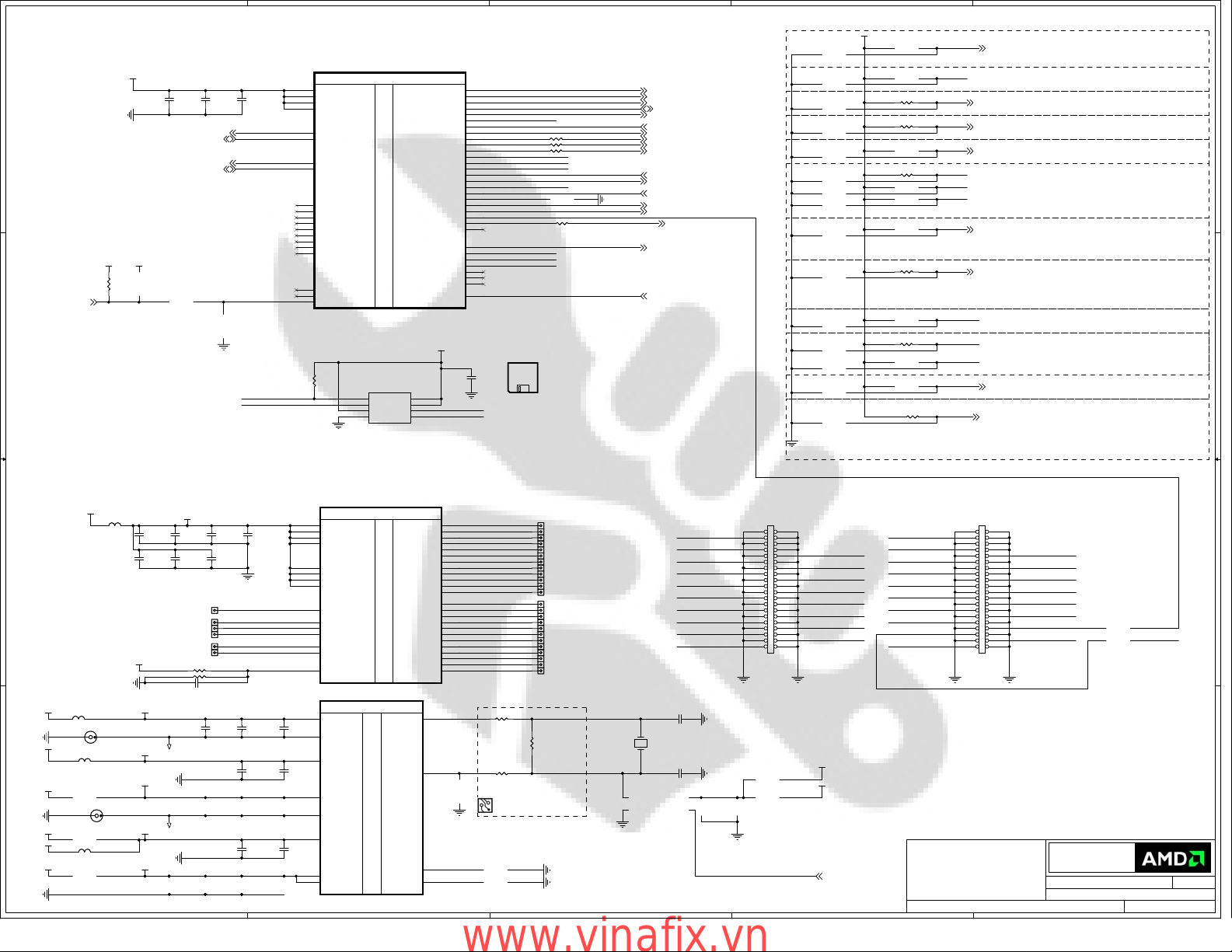
5
(06) RV730 GPIOs Strap CF XTAL
U1E
+3.3V
C332
C332
100nF_6.3V
100nF_6.3V
D D
DDC6CLK(17)
DDC6DATA(17)
+3.3V_BUS +1.8V
R899
R899
5.1K
5.1K
PWR_GOOD(1,14,15,16)
C C
DNI
C333
C333
100nF_6.3V
100nF_6.3V
SCL(17)
SDA(17)
C334
C334
100nF_6.3V
100nF_6.3V
SCL
SDA
DDC6CLK
DDC6DATA
PWR_GOOD_R
DNI
GPIO_22_ROMCSb_R
GPIO_8_R
U1E
AF23
VDDR3#1
AF24
VDDR3#2
AG23
VDDR3#3
AG24
VDDR3#4
AK26
SCL
AJ26
SDA
AJ30
DDC6CLK
AJ31
DDC6DATA
AF28
RSVD#1
AF35
RSVD#2
AG28
RSVD#3
AG36
RSVD#4
AJ27
RSVD#5
AK27
RSVD#6
AL31
RSVD#7
AN36
RSVD#8
AP37
RSVD#9
AJ21
NC#1
AK21
NC#2
AH16
NC_PWRGOOD
RV730XT A12 HF MVE SLT B1
RV730XT A12 HF MVE SLT B1
R180
R180
10K
10K
4
PART 5 OF 15
PART 5 OF 15
G
G
P
P
I
I
O
O
GPIO_17_THERMAL_INT
U2
U2
1
CE#
VCC
2
SO
HOLD#
3
WP#
SCK
GND4SI
PM25LV512A-100SCE
PM25LV512A-100SCE
GPIO_0
GPIO_1
GPIO_2
GPIO_3_SMBDATA
GPIO_4_SMBCLK
GPIO_5_AC_BATT
GPIO_6_TACH
GPIO_7_BLON
GPIO_8_ROMSO
GPIO_9_ROMSI
GPIO_10_ROMSCK
GPIO_11
GPIO_12
GPIO_13
GPIO_14_HPD2
GPIO_15_PWRCNTL_0
GPIO_16_SSIN
GPIO_18_HPD3
GPIO_19_CTF
GPIO_20_PWRCNTL_1
GPIO_21_BB_EN
GPIO_22_ROMCSB
GPIO_23_CLKREQB
GENERICA
GENERICB
GENERICC
GENERICD
GENERICE_HPD4
GENERICF
GENERICG
HPD1
+3.3V
8
7
GPIO_10_R
6
GPIO_9_R
5
AH20
AH18
AN16
AH23
AJ23
AH17
AJ17
AK17
AJ13
AH15
AJ16
AK16
AL16
AM16
AM14
AM13
AK14
AG30
AN14
AM17
AL13
AJ14
AK13
AN13
AJ19
AK19
AJ20
AK20
AJ24
AH26
AH24
AK24
C342
C342
100nF_6.3V
100nF_6.3V
GPIO_0
GPIO_1
GPIO_2
GPIO_3_SMBDATA
GPIO_4_SMBCLK
GPIO_5
GPIO_6_TACH
GPIO_7
GPIO_8
GPIO_9
GPIO_10
GPIO_11
GPIO_12
GPIO_13
HPD2
PWRCNTL_0
GPIO_16
GPIO_17_ThermINT
HPD3
GPIO_19_CTF
PWRCNTL_1
GPIO_21
GPIO_22_ROMCSb
GENERICA
GENERICB
GENERICC
GENERICD
HPD1
BIOS1
BIOS1
BIOS
BIOS
113-B339XX-XXX
113-B339XX-XXX
VIDEO BIOS
FIRMWARE
3
GPIO_0 (17)
GPIO_1 (17)
GPIO_2 (17)
GPIO_3_SMBDATA (1)
GPIO_4_SMBCLK (1)
GPIO_6_TACH (16,17)
GPIO_8_R
RP1C33R RP1C33R
63
GPIO_9_R
RP1B33R RP1B33R
72
GPIO_10_R
RP1A33R RP1A33R
81
DNI DNI
GPIO_22_ROMCSb_R
RP1D33R RP1D33R
54
GPIO_7 (17)
GPIO_8_R (17)
GPIO_9_R (17)
GPIO_10_R (17)
HPD2 (9)
PWRCNTL_0 (15)
GPIO_17_ThermINT (17)
GPIO_19_CTF (16)
PWRCNTL_1 (15)
GPIO_22_ROMCSb_R (17)
GENERICA (7,17)
HPD1 (8)
BUO
2
R149 10KR149 10K
R152 10KR152 10K
R158 10KR158 10K
R161 10KR161 10K
R165 10KR165 10K
R176 10KR176 10K
PIN BASED STRAPS
V2SYNC (7)
V2SYNC
GPIO_9_R
GPIO_0
GPIO_0 (17)
GPIO_1
GPIO_1 (17)
GPIO_2
GPIO_2 (17)
GPIO_13
GPIO_12
GPIO_12
GPIO_11
V1SYNC (7)
V1SYNC
H1SYNC (7)
H1SYNC
GPIO_8_R
GPIO_5
GPIO_16
H2SYNC (7)
H2SYNC
GPIO_7
GPIO_7 (17)
+3.3V
DNI
DNI
DNI
DNI
DNI
DNI
DNI
DNI
DNI
DNI
DNI
DNI
DNI
DNI
DNI
DNI
DNI
DNI
DNI
DNI
DNI
DNI
DNI
DNI
1
VIP_DEVICE_STRAP_EN
0: No slave VIP host port devices reporting presence during reset (use
for configurations without video-in)
1:VIP host port devices present (use if Theater is populated)
VGA DISABLE : 1 for disable (set to 0 for normal operation)
GPIO(0) - TX_PWRS_ENB (Transmitter Power Savings Enable)
0: 50% Tx output swing for mobile mode
1: full Tx output swing (Default setting for Desktop)
GPIO(1) - TX_DEEMPH_EN (Transmitter De-emphasis Enable)
0: Tx de-emphasis disabled for mobile mode
1: Tx de-emphasis enabled (Default setting for Desktop)
GPIO(2) - BIF_GEN2_EN (5.0 GT/s Enable)
0 : Default. (Driver Controlled Gen2)
1 : Strap Controlled Gen2
GPIO(13, 12,11) - CONFIG[2..0]
100 - 512Kbit M25P05A (ST)
101 - 1Mbit M25P10A (ST)
CONFIG[2]
101 - 2Mbit M25P20 (ST)
101 - 4Mbit M25P40 (ST)
CONFIG[1]
101 - 8Mbit M25P80 (ST)
100 - 512Kbit Pm25LV512 (Chingis)
CONFIG[0]
101 - 1Mbit Pm25LV010 (Chingis)
AUD[0] : Enable HD Audio function in the PCI configuration space.
0 - Disable HD Audio
1 - Enable HD Audio
HD audio must only be enabled on systems that are legally
entitled. It is the responsibility of the system designer to
ensure that the system is entitled to support this feature.
AUD[1] : Enable on-board HDMI
Note: Board manufacturer must not set this strap to 1 unless
there is an onboard HDMI connector. It is the
manufacturers responsibility to pay royalties if this strap is
enabled.
This Board doesn't have HDMI Connector
therefore only pull down option is available
BIF_CLK_PM_EN
0 - Disable CLKREQ# power management capability
1 - Enable CLKREQ# power management capability
MEMORY CONFIG
GPIO_5:
0: Single Rank, 1: Dual Rank
RESERVED :Internal use only. Other logic must not affect this signal
during RESET.
ATI Board Feature I
1 - NTSC TVO0 - PAL TVO TV OUT STANDARD
PN 2280007900G for 1Mbit (PM25LV010A-100SCE)
GPIO_21
CrossFire Card-Edge
U1F
+1.8V
B113 BLM15BD121SN1B113 BLM15BD121SN1
B B
+1.8V
+1.8V
B110 BLM15BD121SN1B110 BLM15BD121SN1
NS6 NS_VIANS6 NS_VIA
1 2
+1.1V
B109 BLM15BD121SN1B109 BLM15BD121SN1
+1.8V
A A
NS7 NS_VIANS7 NS_VIA
+1.1V
+VDDC
B107 BLM15BD121SN1B107 BLM15BD121SN1
+1.8V +MPV18
+DPLL_PVDD
+DPLL_VDDC
1 2
5
+SPV18
+SPV10
C327
C327
1uF_6.3V
1uF_6.3V
C325
C325
10uF_X6S
10uF_X6S
VDDR4_5
C326
C326
C335
C335
100nF_6.3V
100nF_6.3V
1uF_6.3V
1uF_6.3V
C331
C331
C329
C329
1uF_6.3V
1uF_6.3V
1uF_6.3V
1uF_6.3V
TP84 35milTP84 35mil
TP85 35milTP85 35mil
TP86 35milTP86 35mil
TP87 35milTP87 35mil
TP88 35milTP88 35mil
TP89 35milTP89 35mil
R147 221RR147 221R
R151 110RR151 110R
C328 100nF_6.3VC328 100nF_6.3V
C147
C147
C148
C148
10uF_X6S
10uF_X6S
1uF_6.3V
1uF_6.3V
GND_DPLL_PVSS
C145
C145
1uF_6.3V
1uF_6.3V
GND_SPVSS
C150
C150
1uF_6.3V
1uF_6.3V
C330
C330
100nF_6.3V
100nF_6.3V
DVOCLK
DVPCNTL_0
DVPCNTL_1
DVPCNTL_2
DVP_MVP_CNTL_0
DVP_MVP_CNTL_1
VREFG
C149
C149
100nF_6.3V
100nF_6.3V
C146
C146
100nF_6.3V
100nF_6.3V
C151
C151
100nF_6.3V
100nF_6.3V
U1F
AD12
VDDR4#1
AF11
VDDR4#2
AF12
VDDR4#3
AG11
VDDR4#4
AF13
VDDR5#1
AF15
VDDR5#2
AG13
VDDR5#3
AG15
VDDR5#4
AR1
DVPCLK
AP8
DVPCNTL_0
AW8
DVPCNTL_1
AR3
DVPCNTL_2
AR8
DVPCNTL_MVP_0
AU8
DVPCNTL_MVP_1
AH13
VREFG
RV730XT A12 HF MVE SLT B1
RV730XT A12 HF MVE SLT B1
U1G
U1G
AM32
DPLL_PVDD
AN32
DPLL_PVSS
AN31
DPLL_VDDC
AM10
NC_SPV18
AN10
SPVSS
AN9
SPV10
H7
NC_MPV18#1
H8
NC_MPV18#2
RV730XT A12 HF MVE SLT B1
RV730XT A12 HF MVE SLT B1
PART 6 OF 15
PART 6 OF 15
PART 7 OF 15
PART 7 OF 15
P
P
L
L
L
L
S
S
X
X
T
T
A
A
L
L
4
D
D
V
V
P
P
DVPDATA_0
DVPDATA_1
DVPDATA_2
DVPDATA_3
DVPDATA_4
DVPDATA_5
DVPDATA_6
DVPDATA_7
DVPDATA_8
DVPDATA_9
DVPDATA_10
DVPDATA_11
DVPDATA_12
DVPDATA_13
DVPDATA_14
DVPDATA_15
DVPDATA_16
DVPDATA_17
DVPDATA_18
DVPDATA_19
DVPDATA_20
DVPDATA_21
DVPDATA_22
DVPDATA_23
XTALOUT
XTALIN
CLKTESTA
CLKTESTB
AU34
AV33
AK10
AL10
DVPDATA_0
AU1
DVPDATA_1
AU3
DVPDATA_2
AW3
DVPDATA_3
AP6
DVPDATA_4
AW5
DVPDATA_5
AU5
DVPDATA_6
AR6
DVPDATA_7
AW6
DVPDATA_8
AU6
DVPDATA_9
AT7
DVPDATA_10
AV7
DVPDATA_11
AN7
DVPDATA_12
AV9
DVPDATA_13
AT9
DVPDATA_14
AR10
DVPDATA_15
AW10
DVPDATA_16
AU10
DVPDATA_17
AP10
DVPDATA_18
AV11
DVPDATA_19
AT11
DVPDATA_20
AR12
DVPDATA_21
AW12
DVPDATA_22
AU12
DVPDATA_23
AP12
XTALOUT
R86 0RR86 0R
R_RTCLK
XTALIN
R81 0RR81 0R
Place R_RTCLK close to XTAL so the
main clock line has shortest stub
CLKTESTA
CLKTESTB
TP6035mil TP6035mil
TP6135mil TP6135mil
TP6235mil TP6235mil
TP6335mil TP6335mil
TP6435mil TP6435mil
TP6535mil TP6535mil
TP6635mil TP6635mil
TP6735mil TP6735mil
TP6835mil TP6835mil
TP6935mil TP6935mil
TP7035mil TP7035mil
TP7135mil TP7135mil
TP7235mil TP7235mil
TP7335mil TP7335mil
TP7435mil TP7435mil
TP7535mil TP7535mil
TP7635mil TP7635mil
TP7735mil TP7735mil
TP7835mil TP7835mil
TP7935mil TP7935mil
TP8035mil TP8035mil
TP8135mil TP8135mil
TP8235mil TP8235mil
TP8335mil TP8335mil
XTALOUT_S
27.000MHz_10PPM
R841MR84
1M
27.000MHz_10PPM
XTALIN_S
3
C83
C83
15pF
15pF
21
Y82
Y82
C82
C82
15pF
15pF
Lower Cable Card Edge
DVPCNTL_2
DVPDATA_1
DVPDATA_3
DVPDATA_5
DVPDATA_7
DVPDATA_9
DVPDATA_11
DVPCNTL_1
GENERICD
or Bundle B or Bundle A (closer to the bracket)
PWR_GOOD
J8002J8002
1
3
5
7
9
11
13
15
17
19
21
23
25
27
29 30
31
33
35
37
39
2
4
6
8
DVPDATA_0
10
12
DVPDATA_2
14
16
DVPDATA_4
18
20
DVPDATA_6
22
24
DVPDATA_8
26
28
DVPDATA_10
32
DVPCNTL_0
34
36
GPIO_2
38
40
+1.8V
+3.3V_BUS
PWR_GOOD (1,14,15,16)
2
Upper Cable Card Edge
J8001J8001
1
DVP_MVP_CNTL_1DVOCLK
DVP_MVP_CNTL_0
DVPDATA_13
DVPDATA_15
DVPDATA_17
DVPDATA_19
DVPDATA_21
DVPDATA_23
GENERICB_R
GENERICC
CONFIDENTIAL & PROPRIETARY TO ADVANCED MICRO DEVICES INC.
CONFIDENTIAL & PROPRIETARY TO ADVANCED MICRO DEVICES INC.
CONFIDENTIAL & PROPRIETARY TO ADVANCED MICRO DEVICES INC.
© 2007 Advanced Micro Devices
© 2007 Advanced Micro Devices
© 2007 Advanced Micro Devices
This AMD Board schematic and design is the exclusive property of AMD,
This AMD Board schematic and design is the exclusive property of AMD,
This AMD Board schematic and design is the exclusive property of AMD,
and is provided only to entities under a non-disclosure agreement
and is provided only to entities under a non-disclosure agreement
and is provided only to entities under a non-disclosure agreement
with AMD for evaluation purposes. Further distribution or disclosure
with AMD for evaluation purposes. Further distribution or disclosure
with AMD for evaluation purposes. Further distribution or disclosure
is strictly prohibited. Use of this schematic and design for any purpose
is strictly prohibited. Use of this schematic and design for any purpose
is strictly prohibited. Use of this schematic and design for any purpose
other than evaluation requires a Board Technology License Agreement
other than evaluation requires a Board Technology License Agreement
other than evaluation requires a Board Technology License Agreement
with AMD. AMD makes no representations or warranties of any kind
with AMD. AMD makes no representations or warranties of any kind
with AMD. AMD makes no representations or warranties of any kind
regarding this schematic and design, including, not limited to,
regarding this schematic and design, including, not limited to,
regarding this schematic and design, including, not limited to,
any implied warranty of merchantibility or fitness for a particular
any implied warranty of merchantibility or fitness for a particular
any implied warranty of merchantibility or fitness for a particular
purpose, and disclaims responsibility forany consequences resulting
purpose, and disclaims responsibility forany consequences resulting
purpose, and disclaims responsibility forany consequences resulting
from use of the information included herein.
from use of the information included herein.
from use of the information included herein.
Title
Title
Title
RH RV730 GDDR3 DVII-TVO-DVII
RH RV730 GDDR3 DVII-TVO-DVII
RH RV730 GDDR3 DVII-TVO-DVII
3
5
7
9
11
13
15
17
19
21
23
25
27
29 30
31
33
35
37
39
2
4
6
8
10
12
14
16
18
20
22
24
26
28
32
34
36
38
40
DVPDATA_12
DVPDATA_14
DVPDATA_16
DVPDATA_18
DVPDATA_20
DVPDATA_22
GPIO_21_R
Advanced Micro Devices Inc.
Advanced Micro Devices Inc.
Advanced Micro Devices Inc.
1 Commerce Valley Drive East
1 Commerce Valley Drive East
1 Commerce Valley Drive East
Markham, Ontario
Markham, Ontario
Markham, Ontario
Sheet
Sheet
Sheet
Do not install for BU
GENERICB: Generic I2C_SDA
DVALID: Generic I2C_SCL
Tuesday, September 02, 2008
Tuesday, September 02, 2008
Tuesday, September 02, 2008
of
619
of
619
of
619
1
Doc No.
Doc No.
Doc No.
GPIO_21
GENERICBGPIO_1
RevDate:
RevDate:
RevDate:
105-B709xx-11
105-B709xx-11
105-B709xx-11
50
50
50
www.vinafix.vn
Page 7

8
(07) RV730 DAC1 and DAC2/TV
+1.8V
B204 BLM15BD121SN1B204 BLM15BD121SN1
NS9 NS_VIANS9 NS_VIA
1 2
+1.8V
B205 BLM15BD121SN1B205 BLM15BD121SN1
D D
NS10 NS_VIANS10 NS_VIA
1 2
+VDD1DI
GND_AVSSQ
GND_AVSSQ
+AVDD
C210
C210
1uF_6.3V
1uF_6.3V
GND_VSS1DI
C213
C213
1uF_6.3V
1uF_6.3V
R110 499RR110 499R
C211
C211
100nF_6.3V
100nF_6.3V
C214
C214
100nF_6.3V
100nF_6.3V
RSET
C212
C212
C215
C215
7
U1H
U1H
PART 8 OF 15
PART 8 OF 15
AC33
10nF
10nF
10nF
10nF
VDD1DI
AC34
VSS1DI
AD34
AVDD
AE34
AVSSQ
AB34
RSET
RV730XT A12 HF MVE SLT B1
RV730XT A12 HF MVE SLT B1
D
D
A
A
C
C
1
1
HSYNC
VSYNC
6
R_DAC1
AD39
R
RB_DAC1
AD37
RB
G_DAC1
AE36
G
GB_DAC1
AD35
GB
B_DAC1
AF37
B
BB_DAC1
AE38
BB
H1SYNC
AC36
V1SYNC
AC38
H1SYNC(6)
V1SYNC(6)
H1SYNC
V1SYNC
R1027 37.4RR1027 37.4R
R1028 37.4RR1028 37.4R
R1029 37.4RR1029 37.4R
C2009
C2009
100nF_6.3V
100nF_6.3V
5
See BOM for qualified filters
Pseudo differential RGB should be routed from the ASIC to the display
connector without switching reference plane or running over split plane.
R1001
R1001
75R
75R
R1002
R1002
75R
75R
R1003
R1003
75R
75R
+5V
U2001A
U2001A
14
74VHC125
74VHC125
74VHC125
74VHC125
U2001B
U2001B
HSYNC_DAC1_B
VSYNC_DAC1_B
2 3
1
7
4
5 6
L1001
L1001
47nH
47nH
L1002
L1002
47nH
47nH
L1003
L1003
47nH
47nH
4
DDC4DATA(8)
DDC4CLK(8)
HSYNC_DAC1_R
10R
10R
R1010
R1010
VSYNC_DAC1_R
10R
10R
R1011
R1011
R1008
R1008
2.2K
2.2K
+5V +5V
3
R1005
R1005
2.2K
2.2K
DDC4DATA
DDC4CLK
+3.3V
R1006 33RR1006 33R
R1009 33RR1009 33R
+5V_VESA
2
A_R_DAC1_F
A_G_DAC1_F
A_B_DAC1_F
DDCDATA_DAC1_R
DDCCLK_DAC1_R
HSYNC_DAC1_R
VSYNC_DAC1_R
VSYNC_DAC1_R (8)
HSYNC_DAC1_R (8)
DDCCLK_DAC1_R (8)
DDCDATA_DAC1_R (8)
A_B_DAC1_F (8)
A_G_DAC1_F (8)
A_R_DAC1_F (8)
603
+5V_VESA
+5V_DAC1_VESA
Overlap pads
1
R10120RR1012
0R
+5V_DAC1_VESA (8)
C C
+1.8V
B201 BLM15BD121SN1B201 BLM15BD121SN1
NS11 NS_VIANS11 NS_VIA
1 2
+1.8V
B203 BLM15BD121SN1B203 BLM15BD121SN1
NS5 NS_VIANS5 NS_VIA
1 2
+3.3V
B202 BLM15BD121SN1B202 BLM15BD121SN1
B B
A A
+VDD2DI
C200
C200
C201
C201
C202
C202
100nF_6.3V
100nF_6.3V
1uF_6.3V
1uF_6.3V
GND_VSS2DI
+A2VDDQ
C207
C207
100nF_6.3V
100nF_6.3V
1uF_6.3V
1uF_6.3V
GND_A2VSSQ
+A2VDD
C203
C203
C204
C204
100nF_6.3V
1uF_6.3V
1uF_6.3V
100nF_6.3V
4.7uF_6.3V
4.7uF_6.3V
GND_A2VSSQ
8
C208
C208
C205
C205
10nF
10nF
C206
C206
10nF
10nF
R2SET
R111715R R111715R
7
U1I
U1I
PART 9 OF 15
PART 9 OF 15
AG31
VDD2DI
AG32
VSS2DI
AD33
A2VDDQ
AF33
A2VSSQ
AG33
A2VDD
AA29
R2SET
RV730XT A12 HF MVE SLT B1
RV730XT A12 HF MVE SLT B1
R_DAC2
AC30
R2
RB_DAC2
AC31
R2B
G_DAC2
AD30
G2
GB_DAC2
AD31
G2B
D
D
A
A
C
C
2
2
/
/
T
T
H2SYNC
V
V
V2SYNC
H2SYNC(6)
V2SYNC(6)
COMP
B_DAC2
AF30
B2
BB_DAC2
AF31
B2B
H2SYNC
AD29
V2SYNC
AC29
Y_DAC2
AD32
Y
C_DAC2
AC32
C
COMP_DAC2
AF32
Y_DAC2
C_DAC2
COMP_DAC2
6
R2027 37.4RR2027 37.4R
R2028 37.4RR2028 37.4R
R2029 37.4RR2029 37.4R
12 11
9 8
Place near connector
0R leaves footprint for Ferrite
Beads if req'd for EMI
R3001
R3001
75R
75R
R3002
R3002
75R
75R
R3003
R3003
75R
75R
See BOM for qualified filters
Pseudo differential RGB should be routed from the ASIC to the display
connector without switching reference plane or running over split plane.
R2001
R2001
75R
75R
402
402
R2002
R2002
75R
75R
402
402 402
R2003
R2003
75R
75R
402 402
402
HSYNC_DAC2_B
U2001D
U2001D
74VHC125
74VHC125
13
10
74VHC125
74VHC125
U2001C
U2001C
VSYNC_DAC2_B
L3001 470nH_250mAL3001 470nH_250mA
C3001
C3001
47pF_50V
47pF_50V
L3002 470nH_250mAL3002 470nH_250mA
C3002
C3002
47pF_50V
47pF_50V
L3003 470nH_250mAL3003 470nH_250mA
C3003
C3003
47pF_50V
47pF_50V
5
C3004
C3004
47pF_50V
47pF_50V
DAC2_C_F
C3005
C3005
47pF_50V
47pF_50V
DAC2_COMP_F
C3006
C3006
47pF_50V
47pF_50V
L2001
L2001
47nH
47nH
L2002
L2002
47nH
47nH
L2003
L2003
47nH
47nH
402
R2010
R2010
R2011
R2011
DAC2_Y_FDAC2_Y_F
DAC2_C_F
DAC2_COMP_F
4
DDC5DATA(9)
DDC5CLK(9)
402
10R
10R
402
10R
10R
Install for Dell
R3004 0RR3004 0R
R3005 0RR3005 0R
R3006 0RR3006 0R
DNI for Dell
R2008
R2008
2.2K
2.2K
HSYNC_DAC2_R
VSYNC_DAC2_R
GENERICA(6,17)
+5V +5V
402
+3.3V
R2005
R2005
2.2K
2.2K
A_R_DAC2_F
A_G_DAC2_F
A_B_DAC2_F
STV/HDTV#_DET
DAC2_Y_DIN
DAC2_C_DIN
DAC2_COMP_DIN
3
R2006 33RR2006 33R
R2009 33RR2009 33R
+3.3V
R3008
R3008
10K
10K
+5V_VESA
DDCDATA_DAC2_R
DDCCLK_DAC2_R
HSYNC_DAC2_R
VSYNC_DAC2_R
VSYNC_DAC2_R (9)
HSYNC_DAC2_R (9)
DDCCLK_DAC2_R (9)
DDCDATA_DAC2_R (9)
A_B_DAC2_F (9)
A_G_DAC2_F (9)
A_R_DAC2_F (9)
Install for Dell
R3009 0RR3009 0R
Install for Dell only when it's needed for EMI
R30070RR3007
0R
DNI for Dell
CONFIDENTIAL & PROPRIETARY TO ADVANCED MICRO DEVICES INC.
CONFIDENTIAL & PROPRIETARY TO ADVANCED MICRO DEVICES INC.
CONFIDENTIAL & PROPRIETARY TO ADVANCED MICRO DEVICES INC.
© 2007 Advanced Micro Devices
© 2007 Advanced Micro Devices
© 2007 Advanced Micro Devices
This AMD Board schematic and design is the exclusive property of AMD,
This AMD Board schematic and design is the exclusive property of AMD,
This AMD Board schematic and design is the exclusive property of AMD,
and is provided only to entities under a non-disclosure agreement
and is provided only to entities under a non-disclosure agreement
and is provided only to entities under a non-disclosure agreement
with AMD for evaluation purposes. Further distribution or disclosure
with AMD for evaluation purposes. Further distribution or disclosure
with AMD for evaluation purposes. Further distribution or disclosure
is strictly prohibited. Use of this schematic and design for any purpose
is strictly prohibited. Use of this schematic and design for any purpose
is strictly prohibited. Use of this schematic and design for any purpose
other than evaluation requires a Board Technology License Agreement
other than evaluation requires a Board Technology License Agreement
other than evaluation requires a Board Technology License Agreement
with AMD. AMD makes no representations or warranties of any kind
with AMD. AMD makes no representations or warranties of any kind
with AMD. AMD makes no representations or warranties of any kind
regarding this schematic and design, including, not limited to,
regarding this schematic and design, including, not limited to,
regarding this schematic and design, including, not limited to,
any implied warranty of merchantibility or fitness for a particular
any implied warranty of merchantibility or fitness for a particular
any implied warranty of merchantibility or fitness for a particular
purpose, and disclaims responsibility forany consequences resulting
purpose, and disclaims responsibility forany consequences resulting
purpose, and disclaims responsibility forany consequences resulting
from use of the information included herein.
from use of the information included herein.
from use of the information included herein.
Title
Title
Title
RH RV730 GDDR3 DVII-TVO-DVII
RH RV730 GDDR3 DVII-TVO-DVII
RH RV730 GDDR3 DVII-TVO-DVII
2
+5V_VESA
+5V_DAC2_VESA
603
TV Out
J3001
J3001
PIN6
6
HDTV_OUT_DET#
3
Y-OUT
4
C-OUT
7
Comp_out
CompIn
5
SYNC
1
GND
2
GND#2
8
Rpin5
CASE
9
CASE#9
10
CASE#10
Conn_DIN_Mini_Circular_7_Pin_with_O_Ring
Conn_DIN_Mini_Circular_7_Pin_with_O_Ring
Advanced Micro Devices Inc.
Advanced Micro Devices Inc.
Advanced Micro Devices Inc.
1 Commerce Valley Drive East
1 Commerce Valley Drive East
1 Commerce Valley Drive East
Markham, Ontario
Markham, Ontario
Markham, Ontario
Tuesday, September 02, 2008
Tuesday, September 02, 2008
Tuesday, September 02, 2008
Sheet
Sheet
Sheet
of
719
of
719
of
719
R20120RR2012
0R
Overlap pads
Doc No.
Doc No.
Doc No.
+5V_DAC2_VESA (9)
RevDate:
RevDate:
RevDate:
105-B709xx-11
105-B709xx-11
105-B709xx-11
1
50
50
50
www.vinafix.vn
Page 8

8
7
6
5
4
3
2
1
(08) RV730 TMDS A&B
D D
U1J
ABTX5P
ABTX5M
ABTX4P
ABTX4M
ABTX3P
ABTX3M
AU28
AV27
AV29
AR28
AP31
AP32
AN33
AP33
AN24
AP24
AP25
AP26
AW28
AN27
AP28
AP27
AW24
AW26
AP30
AN29
AP29
AW30
AW32
U1J
RV730XT A12 HF MVE SLT B1
RV730XT A12 HF MVE SLT B1
DPA_PVDD
DPA_PVSS
DPB_PVDD
DPB_PVSS
DPA_VDD10#1
DPA_VDD10#2
DPB_VDD10#1
DPB_VDD10#2
NC_DPA_VDD18#1
NC_DPA_VDD18#2
NC_DPB_VDD18#1
NC_DPB_VDD18#2
DPAB_CALR
DPA_VSSR#1
DPA_VSSR#3
DPA_VSSR#2
DPA_VSSR#4
DPA_VSSR#5
DPB_VSSR#3
DPB_VSSR#1
DPB_VSSR#2
DPB_VSSR#4
DPB_VSSR#5
PART 10 OF 15
PART 10 OF 15
T
T
M
M
D
D
P
P
A
A
/
/
B
B
TX2P_DPA0P
TX2M_DPA0N
TX1P_DPA1P
TX1M_DPA1N
TX0P_DPA2P
TX0M_DPA2N
TXCAP_DPA3P
TXCAM_DPA3N
DDC1CLK
DDC1DATA
TX5P_DPB0P
TX5M_DPB0N
TX4P_DPB1P
TX4M_DPB1N
TX3P_DPB2P
TX3M_DPB2N
TXCBP_DPB3P
TXCBM_DPB3N
DDCCLK_AUX4P
DDCDATA_AUX4N
ABTX5P
ABTX5M
ABTX4P
ABTX4M
ABTX3P
ABTX3M
AUX1P
AUX1N
AT27
AR26
AU26
AV25
AT25
AR24
AU24
AV23
AM27
AL27
AM26
AN26
AT33
AU32
AR32
AT31
AV31
AU30
AR30
AT29
AL29
AM29
DPA_TX2P
DPA_TX2N
DPA_TX1P
DPA_TX0P
DPA_TX0N
DPA_TXCAP
DPA_TXCAN
DPB_TX5P
DPB_TX5N
DPB_TX4P
DPB_TX4N
DPB_TX3N
DDC4CLK
DDC4DATA
C1120 100nF_6.3VC1120 100nF_6.3V
C1121 100nF_6.3VC1121 100nF_6.3V
C1122 100nF_6.3VC1122 100nF_6.3V
C1123 100nF_6.3VC1123 100nF_6.3V
C1124 100nF_6.3VC1124 100nF_6.3V
C1125 100nF_6.3VC1125 100nF_6.3V
C1126 100nF_6.3VC1126 100nF_6.3V
C1127 100nF_6.3VC1127 100nF_6.3V
C1132 100nF_6.3VC1132 100nF_6.3V
C1133 100nF_6.3VC1133 100nF_6.3V
C1134 100nF_6.3VC1134 100nF_6.3V
C1135 100nF_6.3VC1135 100nF_6.3V
C1136 100nF_6.3VC1136 100nF_6.3V
C1137 100nF_6.3VC1137 100nF_6.3V
DDC4CLK (7)
DDC4DATA (7)
R1120 499RR1120 499R
R1122 499RR1122 499R
R1124 499RR1124 499R
R1126 499RR1126 499R
R1132 499RR1132 499R
R1134 499RR1134 499R
R1136 499RR1136 499R
ALL_RAILS_UP(9,15)
R1121 499RR1121 499R
R1123 499RR1123 499R
R1125 499RR1125 499R
R1127 499RR1127 499R
R1133 499RR1133 499R
R1135 499RR1135 499R
R1137 499RR1137 499R
DPAB_GND
ABTX2P
ABTX2M
ABTX1P
ABTX1MDPA_TX1N
ABTX0P
ABTX0M
ABTXCP
ABTXCM
ABTX5P
ABTX5M
ABTX4P
ABTX4M
ABTX3PDPB_TX3P
ABTX3M
32
Q1110
Q1110
SI2304DS
SI2304DS
1
HPD1(6)
Q1021
Q1021
MMBT3904
MMBT3904
+5V_DAC1_VESA(7)
DDCCLK_DAC1_R(7)
DDCDATA_DAC1_R(7)
VSYNC_DAC1_R(7)
A_R_DAC1_F(7)
A_G_DAC1_F(7)
A_B_DAC1_F(7)
HSYNC_DAC1_R(7)
+3.3V
1
2 3
R1023
R1023
10K
10K
R1022 10KR1022 10K
+5V_DAC1_VESA
ABTX2M
ABTX2P
ABTX4M
ABTX4P
DDCCLK_DAC1_R
DDCDATA_DAC1_R
VSYNC_DAC1_R
ABTX1M
ABTX1P
ABTX3M
ABTX3P
ABTX0M
ABTX0P
ABTX5M
ABTX5P
ABTXCP
ABTXCM
A_R_DAC1_F
A_G_DAC1_F
A_B_DAC1_F
HSYNC_DAC1_R
HPD_DVIAB
J1001
J1001
25
CASE
1
TMDS Data2-
2
TMDS Data2+
3
TMDS Data2/4 Shield
4
TMDS Data4-
5
TMDS Data4+
6
DDC Clock
7
DDC Data
8
Analog VSYNC
9
TMDS Data1-
10
TMDS Data1+
11
TMDS Data1/3 Shield
12
TMDS Data3-
13
TMDS Data3+
14
+5V Power
15
GND (for +5V)
16
Hot Plug Detect
17
TMDS Data0-
18
TMDS Data0+
19
TMDS Data0/5 Shield
20
TMDS Data5-
21
TMDS Data5+
22
TMDS Clock Shield
23
TMDS Clock+
24
TMDS Clock-
C1
Analog Red
C2
Analog Green
C3
Analog Blue
C4
Analog HYNC
C5
Analog GND
C6
Analog GND#C6
26
CASE#26
27
CASE#27
28
CASE#28
29
CASE#29
30
CASE#30
DVI_CONNECTOR
DVI_CONNECTOR
C104
C104
100nF
100nF
GND_DPABVSS
C110
C110
100nF
100nF
R130150R R130150R
+DPAB_PVDD
+DPAB_VDD10
+DPAB_VDD18
DPAB_CALR
+1.8V
B102 BLM15BD121SN1B102 BLM15BD121SN1
C102
C102
C106
C106
4.7uF_6.3V
4.7uF_6.3V
1uF_6.3V
1uF_6.3V
NS1NS_VIA NS1NS_VIA
1 2
+1.1V
B104 BLM15BD121SN1B104 BLM15BD121SN1
C C
+1.8V
B B
C112
C112
1uF_6.3V
1uF_6.3V
4.7uF_6.3V
4.7uF_6.3V
C108
C108
C103
C103
1uF_6.3V
1uF_6.3V
C109
C109
1uF_6.3V
1uF_6.3V
ESD protection dioes
ABTX2P
ABTX2M
ABTX1P
ABTX1M
ABTX0P
ABTX0M
ABTXCP
ABTXCM
ABTX2P
ABTX2M
ABTX1P
ABTX1M
ABTX0P
ABTX0M
ABTXCP
ABTXCM
A A
CONFIDENTIAL & PROPRIETARY TO ADVANCED MICRO DEVICES INC.
CONFIDENTIAL & PROPRIETARY TO ADVANCED MICRO DEVICES INC.
CONFIDENTIAL & PROPRIETARY TO ADVANCED MICRO DEVICES INC.
© 2007 Advanced Micro Devices
© 2007 Advanced Micro Devices
© 2007 Advanced Micro Devices
This AMD Board schematic and design is the exclusive property of AMD,
This AMD Board schematic and design is the exclusive property of AMD,
This AMD Board schematic and design is the exclusive property of AMD,
and is provided only to entities under a non-disclosure agreement
and is provided only to entities under a non-disclosure agreement
and is provided only to entities under a non-disclosure agreement
with AMD for evaluation purposes. Further distribution or disclosure
with AMD for evaluation purposes. Further distribution or disclosure
with AMD for evaluation purposes. Further distribution or disclosure
is strictly prohibited. Use of this schematic and design for any purpose
is strictly prohibited. Use of this schematic and design for any purpose
is strictly prohibited. Use of this schematic and design for any purpose
other than evaluation requires a Board Technology License Agreement
other than evaluation requires a Board Technology License Agreement
other than evaluation requires a Board Technology License Agreement
with AMD. AMD makes no representations or warranties of any kind
with AMD. AMD makes no representations or warranties of any kind
with AMD. AMD makes no representations or warranties of any kind
regarding this schematic and design, including, not limited to,
regarding this schematic and design, including, not limited to,
regarding this schematic and design, including, not limited to,
any implied warranty of merchantibility or fitness for a particular
any implied warranty of merchantibility or fitness for a particular
any implied warranty of merchantibility or fitness for a particular
purpose, and disclaims responsibility forany consequences resulting
purpose, and disclaims responsibility forany consequences resulting
purpose, and disclaims responsibility forany consequences resulting
from use of the information included herein.
from use of the information included herein.
from use of the information included herein.
Title
Title
8
7
6
5
4
3
Title
RH RV730 GDDR3 DVII-TVO-DVII
RH RV730 GDDR3 DVII-TVO-DVII
RH RV730 GDDR3 DVII-TVO-DVII
2
Advanced Micro Devices Inc.
Advanced Micro Devices Inc.
Advanced Micro Devices Inc.
1 Commerce Valley Drive East
1 Commerce Valley Drive East
1 Commerce Valley Drive East
Markham, Ontario
Markham, Ontario
Markham, Ontario
Tuesday, September 02, 2008
Tuesday, September 02, 2008
Tuesday, September 02, 2008
Sheet
Sheet
Sheet
of
819
of
819
of
819
Doc No.
Doc No.
Doc No.
1
RevDate:
RevDate:
RevDate:
50
50
50
105-B709xx-11
105-B709xx-11
105-B709xx-11
www.vinafix.vn
Page 9

8
7
(09) RV730 Display Port C&D
6
5
4
3
2
1
D D
C C
B B
+1.8V
BLM15BD121SN1
BLM15BD121SN1
NS3 NS_VIANS3 NS_VIA
1 2
+1.1V
BLM15BD121SN1
BLM15BD121SN1
B124
B124
+1.8V
B122
B122
C122
C122
4.7uF_6.3V
4.7uF_6.3V
C128
C128
4.7uF_6.3V
4.7uF_6.3V
C123
C123
1uF_6.3V
1uF_6.3V
C129
C129
1uF_6.3V
1uF_6.3V
C124
C124
100nF
100nF
GND_DPCDVSS
C130
C130
100nF
100nF
R109150R R109150R
+DPCD_PVDD
+DPCD_VDD10
+DPCD_VDD18
DPCD_CALR
ESD protection dioes
CDTX2P
CDTX2M
CDTX1P CDTX1P
CDTX1M
CDTX0P
CDTX0M
CDTXCP
CDTXCM
A A
CDTX2P
CDTX2M
CDTX1M
CDTX0P
CDTX0M
CDTXCP
CDTXCM
CDTX5P
CDTX5M
CDTX4P
CDTX4M
CDTX3P
CDTX3M
U1K
U1K
AU18
DPC_PVDD
AV17
DPC_PVSS
AV19
DPD_PVDD
AR18
DPD_PVSS
AP13
DPC_VDD10#1
AT13
DPC_VDD10#2
AP14
DPD_VDD10#1
AP15
DPD_VDD10#2
AP20
NC_DPC_VDD18#1
AP21
NC_DPC_VDD18#2
AP22
NC_DPD_VDD18#1
AP23
NC_DPD_VDD18#2
AW18
DPCD_CALR
AN17
DPC_VSSR#1
AP16
DPC_VSSR#2
AP17
DPC_VSSR#3
AW14
DPC_VSSR#4
AW16
DPC_VSSR#5
AN19
DPD_VSSR#1
AP18
DPD_VSSR#2
AP19
DPD_VSSR#3
AW20
DPD_VSSR#4
AW22
DPD_VSSR#5
RV730XT A12 HF MVE SLT B1
RV730XT A12 HF MVE SLT B1
PART 11 OF 15
PART 11 OF 15
T
T
M
M
D
D
P
P
C
C
/
/
D
D
CDTX5P
CDTX5M
CDTX4P
CDTX4M
CDTX3P
CDTX3M
TX2P_DPC0P
TX2M_DPC0N
TX1P_DPC1P
TX1M_DPC1N
TX0P_DPC2P
TX0M_DPC2N
TXCCP_DPC3P
TXCCM_DPC3N
AUX2P
AUX2N
DDC2CLK
DDC2DATA
TX5P_DPD0P
TX5M_DPD0N
TX4P_DPD1P
TX4M_DPD1N
TX3P_DPD2P
TX3M_DPD2N
TXCDP_DPD3P
TXCDM_DPD3N
DDCCLK_AUX5P
DDCDATA_AUX5N
AT17
AR16
AU16
AV15
AT15
AR14
AU14
AV13
AN20
AM20
AM19
AL19
AT23
AR22
AU22
AV21
AT21
AR20
AU20
AT19
AN21
AM21
DPC_TX2P
DPC_TX2N
DPC_TX1P
DPC_TX1N
DPC_TX0N
DPC_TXCCP
DPC_TXCCN
DPD_TX5P
DPD_TX5N
DPD_TX4P
DPD_TX4N
DPD_TX3P
DPD_TX3N
DDCAUX5P
DDCAUX5N
C2120 100nF_6.3VC2120 100nF_6.3V
C2121 100nF_6.3VC2121 100nF_6.3V
C2122 100nF_6.3VC2122 100nF_6.3V
C2123 100nF_6.3VC2123 100nF_6.3V
C2124 100nF_6.3VC2124 100nF_6.3V
C2125 100nF_6.3VC2125 100nF_6.3V
C2126 100nF_6.3VC2126 100nF_6.3V
C2127 100nF_6.3VC2127 100nF_6.3V
C2130 100nF_6.3VC2130 100nF_6.3V
C2131 100nF_6.3VC2131 100nF_6.3V
C2132 100nF_6.3VC2132 100nF_6.3V
C2133 100nF_6.3VC2133 100nF_6.3V
C2134 100nF_6.3VC2134 100nF_6.3V
C2135 100nF_6.3VC2135 100nF_6.3V
DDC5CLK (7)
DDC5DATA (7)
R2120 499RR2120 499R
R2122 499RR2122 499R
R2124 499RR2124 499R
R2126 499RR2126 499R
R2132 499RR2132 499R
R2134 499RR2134 499R
R2136 499RR2136 499R
ALL_RAILS_UP(8,15)
R2121 499RR2121 499R
R2123 499RR2123 499R
R2125 499RR2125 499R
R2127 499RR2127 499R
R2133 499RR2133 499R
R2135 499RR2135 499R
R2137 499RR2137 499R
DPCD_GND
CDTX2P
CDTX2M
CDTX1P
CDTX1M
CDTX0PDPC_TX0P
CDTX0M
CDTXCP
CDTXCM
CDTX5P
CDTX5M
CDTX4P
CDTX4M
CDTX3P
CDTX3M
32
Q2110
Q2110
SI2304DS
SI2304DS
1
HPD2(6)
Q7002
Q7002
MMBT3904
MMBT3904
+3.3V
+5V_DAC2_VESA(7)
DDCCLK_DAC2_R(7)
DDCDATA_DAC2_R(7)
VSYNC_DAC2_R(7)
A_R_DAC2_F(7)
A_G_DAC2_F(7)
A_B_DAC2_F(7)
HSYNC_DAC2_R(7)
2 3
R7006
R7006
10K
10K
R7003 10KR7003 10K
1
+5V_DAC2_VESA
CDTX2M
CDTX2P
CDTX4M
CDTX4P
DDCCLK_DAC2_R
DDCDATA_DAC2_R
VSYNC_DAC2_R
CDTX1M
CDTX1P
CDTX3M
CDTX3P
CDTX0M
CDTX0P
CDTX5M
CDTX5P
CDTXCP
CDTXCM
A_R_DAC2_F
A_G_DAC2_F
A_B_DAC2_F
HSYNC_DAC2_R
HPD_DVICD
J2001
J2001
25
CASE
1
TMDS Data2-
2
TMDS Data2+
3
TMDS Data2/4 Shield
4
TMDS Data4-
5
TMDS Data4+
6
DDC Clock
7
DDC Data
8
Analog VSYNC
9
TMDS Data1-
10
TMDS Data1+
11
TMDS Data1/3 Shield
12
TMDS Data3-
13
TMDS Data3+
14
+5V Power
15
GND (for +5V)
16
Hot Plug Detect
17
TMDS Data0-
18
TMDS Data0+
19
TMDS Data0/5 Shield
20
TMDS Data5-
21
TMDS Data5+
22
TMDS Clock Shield
23
TMDS Clock+
24
TMDS Clock-
C1
Analog Red
C2
Analog Green
C3
Analog Blue
C4
Analog HYNC
C5
Analog GND
C6
Analog GND#C6
26
CASE#26
27
CASE#27
28
CASE#28
29
CASE#29
30
CASE#30
DVI_CONNECTOR
DVI_CONNECTOR
CONFIDENTIAL & PROPRIETARY TO ADVANCED MICRO DEVICES INC.
CONFIDENTIAL & PROPRIETARY TO ADVANCED MICRO DEVICES INC.
CONFIDENTIAL & PROPRIETARY TO ADVANCED MICRO DEVICES INC.
© 2007 Advanced Micro Devices
© 2007 Advanced Micro Devices
© 2007 Advanced Micro Devices
This AMD Board schematic and design is the exclusive property of AMD,
This AMD Board schematic and design is the exclusive property of AMD,
This AMD Board schematic and design is the exclusive property of AMD,
and is provided only to entities under a non-disclosure agreement
and is provided only to entities under a non-disclosure agreement
and is provided only to entities under a non-disclosure agreement
with AMD for evaluation purposes. Further distribution or disclosure
with AMD for evaluation purposes. Further distribution or disclosure
with AMD for evaluation purposes. Further distribution or disclosure
is strictly prohibited. Use of this schematic and design for any purpose
is strictly prohibited. Use of this schematic and design for any purpose
is strictly prohibited. Use of this schematic and design for any purpose
other than evaluation requires a Board Technology License Agreement
other than evaluation requires a Board Technology License Agreement
other than evaluation requires a Board Technology License Agreement
with AMD. AMD makes no representations or warranties of any kind
with AMD. AMD makes no representations or warranties of any kind
with AMD. AMD makes no representations or warranties of any kind
regarding this schematic and design, including, not limited to,
regarding this schematic and design, including, not limited to,
regarding this schematic and design, including, not limited to,
any implied warranty of merchantibility or fitness for a particular
any implied warranty of merchantibility or fitness for a particular
any implied warranty of merchantibility or fitness for a particular
purpose, and disclaims responsibility forany consequences resulting
purpose, and disclaims responsibility forany consequences resulting
purpose, and disclaims responsibility forany consequences resulting
from use of the information included herein.
from use of the information included herein.
from use of the information included herein.
Title
Title
8
7
6
5
4
3
Title
RH RV730 GDDR3 DVII-TVO-DVII
RH RV730 GDDR3 DVII-TVO-DVII
RH RV730 GDDR3 DVII-TVO-DVII
2
Advanced Micro Devices Inc.
Advanced Micro Devices Inc.
Advanced Micro Devices Inc.
1 Commerce Valley Drive East
1 Commerce Valley Drive East
1 Commerce Valley Drive East
Markham, Ontario
Markham, Ontario
Markham, Ontario
Tuesday, September 02, 2008
Tuesday, September 02, 2008
Tuesday, September 02, 2008
Sheet
Sheet
Sheet
of
919
of
919
of
919
Doc No.
Doc No.
Doc No.
1
RevDate:
RevDate:
RevDate:
50
50
50
105-B709xx-11
105-B709xx-11
105-B709xx-11
www.vinafix.vn
Page 10

8
7
6
5
4
3
2
1
(10) No Connect E&F
D D
U1L
U1L
AM37
AN38
AL38
C C
AM35
AM33
AL33
AK34
AK33
AJ34
AH34
DPE_PVDD
DPE_PVSS
NC_DPF_PVDD
NC_DPF_PVSS
DPE_VDD10#2
DPE_VDD10#1
DPF_VDD10#2
DPF_VDD10#1
DPE_VDD18#2
DPE_VDD18#1
PART 12 OF 15
PART 12 OF 15
L
L
V
V
T
T
M
M
D
D
P
P
E
E
/
/
F
F
T2X2P_DPE0P
T2X2M_DPE0N
T2X1P_DPE1P
T2X1M_DPE1N
T2X0P_DPE2P
T2X0M_DPE2N
T2XCEP_DPE3P
T2XCEM_DPE3N
DDCCLK_AUX3P
DDCDATA_AUX3N
AP35
AR35
AR37
AU39
AW37
AU35
AP34
AR34
AL30
AM30
AG38
AG34
DPF_VDD18#2
AF34
DPF_VDD18#1
DPEF_CALR
R133150R R133150R
B B
A A
8
7
AM39
DPEF_CALR
AN34
DPE_VSSR#1
AP39
DPE_VSSR#2
AR39
DPE_VSSR#3
AU37
DPE_VSSR#4
AW35
DPE_VSSR#5
AF39
DPF_VSSR#1
AL34
DPF_VSSR#4
AH39
DPF_VSSR#2
AM34
DPF_VSSR#5
AK39
DPF_VSSR#3
RV730XT A12 HF MVE SLT B1
RV730XT A12 HF MVE SLT B1
6
T2X5P_DPF0P
T2X5M_DPF0N
T2X4P_DPF1P
T2X4M_DPF1N
T2X3P_DPF2P
T2X3M_DPF2N
T2XCFM_DPF3N
T2XCFP_DPF3P
NC_DDCCLK_AUX7P
NC_DDCDATA_AUX7N
5
AH37
AH35
AJ36
AJ38
AK37
AL36
AK35
AK30
AK29
CONFIDENTIAL & PROPRIETARY TO ADVANCED MICRO DEVICES INC.
CONFIDENTIAL & PROPRIETARY TO ADVANCED MICRO DEVICES INC.
CONFIDENTIAL & PROPRIETARY TO ADVANCED MICRO DEVICES INC.
© 2007 Advanced Micro Devices
© 2007 Advanced Micro Devices
© 2007 Advanced Micro Devices
This AMD Board schematic and design is the exclusive property of AMD,
This AMD Board schematic and design is the exclusive property of AMD,
This AMD Board schematic and design is the exclusive property of AMD,
and is provided only to entities under a non-disclosure agreement
and is provided only to entities under a non-disclosure agreement
and is provided only to entities under a non-disclosure agreement
with AMD for evaluation purposes. Further distribution or disclosure
with AMD for evaluation purposes. Further distribution or disclosure
with AMD for evaluation purposes. Further distribution or disclosure
is strictly prohibited. Use of this schematic and design for any purpose
is strictly prohibited. Use of this schematic and design for any purpose
is strictly prohibited. Use of this schematic and design for any purpose
other than evaluation requires a Board Technology License Agreement
other than evaluation requires a Board Technology License Agreement
other than evaluation requires a Board Technology License Agreement
with AMD. AMD makes no representations or warranties of any kind
with AMD. AMD makes no representations or warranties of any kind
with AMD. AMD makes no representations or warranties of any kind
regarding this schematic and design, including, not limited to,
regarding this schematic and design, including, not limited to,
regarding this schematic and design, including, not limited to,
any implied warranty of merchantibility or fitness for a particular
any implied warranty of merchantibility or fitness for a particular
any implied warranty of merchantibility or fitness for a particular
purpose, and disclaims responsibility forany consequences resulting
purpose, and disclaims responsibility forany consequences resulting
purpose, and disclaims responsibility forany consequences resulting
from use of the information included herein.
from use of the information included herein.
from use of the information included herein.
Title
Title
4
3
Title
RH RV730 GDDR3 DVII-TVO-DVII
RH RV730 GDDR3 DVII-TVO-DVII
RH RV730 GDDR3 DVII-TVO-DVII
2
Advanced Micro Devices Inc.
Advanced Micro Devices Inc.
Advanced Micro Devices Inc.
1 Commerce Valley Drive East
1 Commerce Valley Drive East
1 Commerce Valley Drive East
Markham, Ontario
Markham, Ontario
Markham, Ontario
Tuesday, September 02, 2008
Tuesday, September 02, 2008
Tuesday, September 02, 2008
Sheet
Sheet
Sheet
of
10 19
of
10 19
of
10 19
Doc No.
Doc No.
Doc No.
1
RevDate:
RevDate:
RevDate:
50
50
50
105-B709xx-11
105-B709xx-11
105-B709xx-11
www.vinafix.vn
Page 11

5
(11) RV730 Power & GND
4
3
2
1
C277
C277
1uF_6.3V
1uF_6.3V
C170
C170
1uF_6.3V
1uF_6.3V
C180
C180
1uF_6.3V
1uF_6.3V
C941
C941
1uF_6.3V
1uF_6.3V
MC194
MC194
4.7uF_6.3V
4.7uF_6.3V
+VDDC
C942
C942
1uF_6.3V
1uF_6.3V
U1N
U1N
B31
GND#91
B33
GND#92
B7
GND#93
B9
GND#94
C1
GND#95
C39
GND#96
E35
GND#97
E5
GND#98
F11
GND#99
F13
GND#100
F15
GND#101
F17
GND#102
F19
GND#103
F21
GND#104
F23
GND#105
F25
GND#106
F27
GND#107
F29
GND#108
F31
GND#109
F33
GND#110
F7
GND#111
F9
GND#112
G2
GND#113
G6
GND#114
H9
GND#115
J2
GND#116
J27
GND#117
J6
GND#118
J8
GND#119
K14
GND#120
K7
GND#121
L11
GND#122
L17
GND#123
L2
GND#124
L22
GND#125
L24
GND#126
L6
GND#127
M17
GND#128
M22
GND#129
M24
GND#130
N16
GND#131
N18
GND#132
N2
GND#133
N21
GND#134
N23
GND#135
N26
GND#136
N6
GND#137
R15
GND#138
R17
GND#139
R2
GND#140
R20
GND#141
R22
GND#142
R24
GND#143
R27
GND#144
R6
GND#145
T11
GND#146
T13
GND#147
T16
GND#148
T18
GND#149
T21
GND#150
T23
GND#151
T26
GND#152
U13
GND#153
U15
GND#154
U17
GND#155
U2
GND#156
U20
GND#157
U22
GND#158
U24
GND#159
U27
GND#160
U6
GND#161
V11
GND#162
V13
GND#163
V16
GND#164
V18
GND#165
V21
GND#166
V23
GND#167
V26
GND#168
W2
GND#169
W6
GND#170
Y15
GND#171
Y17
GND#172
Y20
GND#173
Y22
GND#174
Y24
GND#175
Y27
GND#176
A39
VSS_MECH#1
AW1
VSS_MECH#2
AW39
VSS_MECH#3
RV730XT A12 HF MVE SLT B1
RV730XT A12 HF MVE SLT B1
PART 14 OF 15
PART 14 OF 15
G
G
N
N
D
D
GND#1
GND#2
GND#3
GND#4
GND#5
GND#6
GND#7
GND#8
GND#9
GND#10
GND#11
GND#12
GND#13
GND#14
GND#15
GND#16
GND#17
GND#18
GND#19
GND#20
GND#21
GND#22
GND#23
GND#24
GND#25
GND#26
GND#27
GND#28
GND#29
GND#30
GND#31
GND#32
GND#33
GND#34
GND#35
GND#36
GND#37
GND#38
GND#39
GND#40
GND#41
GND#42
GND#43
GND#44
GND#45
GND#46
GND#47
GND#48
GND#49
GND#50
GND#51
GND#52
GND#53
GND#54
GND#55
GND#56
GND#57
GND#58
GND#59
GND#60
GND#61
GND#62
GND#63
GND#64
GND#65
GND#66
GND#67
GND#68
GND#69
GND#70
GND#71
GND#72
GND#73
GND#74
GND#75
GND#76
GND#77
GND#78
GND#79
GND#80
GND#81
GND#82
GND#83
GND#84
GND#85
GND#86
GND#87
GND#88
GND#89
GND#90
A3
A37
AA16
AA18
AA2
AA21
AA23
AA26
AA28
AA6
AB12
AB15
AB17
AB20
AB22
AB24
AB27
AC11
AC13
AC16
AC18
AC2
AC21
AC23
AC26
AC28
AC6
AD15
AD17
AD20
AD22
AD24
AD27
AD9
AE2
AE6
AF10
AF16
AF18
AF21
AG17
AG2
AG20
AG22
AG6
AG9
AH21
AH29
AJ10
AJ11
AJ2
AJ28
AJ6
AK11
AK31
AK7
AL11
AL14
AL17
AL2
AL20
AL21
AL23
AL26
AL32
AL6
AL8
AM11
AM31
AM9
AN11
AN2
AN30
AN6
AN8
AP11
AP7
AP9
AR5
AW34
B11
B13
B15
B17
B19
B21
B23
B25
B27
B29
Swap With C1225, C1226, C1227, C1228, C1229,
C1230, C1231, C1232, C1233, C1272, C1273, C1274
refdes locations
C2402
C2402
C2411
C2400
C2400
100nF_6.3V
100nF_6.3V
C284
C284
1uF_6.3V
1uF_6.3V
C2410
C2410
1uF_6.3V
1uF_6.3V
C2254
C2254
1uF_6.3V
1uF_6.3V
C2411
100nF_6.3V
100nF_6.3V
C2403
C2403
1uF_6.3V
1uF_6.3V
C285
C285
1uF_6.3V
1uF_6.3V
C2267
C2267
1uF_6.3V
1uF_6.3V
100nF_6.3V
100nF_6.3V
C278
C278
1uF_6.3V
1uF_6.3V
C2404
C2404
1uF_6.3V
1uF_6.3V
C2412
C2412
1uF_6.3V
1uF_6.3V
C279
C279
1uF_6.3V
1uF_6.3V
C287
C287
1uF_6.3V
1uF_6.3V
C2405
C2405
1uF_6.3V
1uF_6.3V
C2413
C2413
1uF_6.3V
1uF_6.3V
C280
C280
1uF_6.3V
1uF_6.3V
C288
C288
1uF_6.3V
1uF_6.3V
C2406
C2406
1uF_6.3V
1uF_6.3V
C2414
C2414
1uF_6.3V
1uF_6.3V
C286
C286
C2409
C2409
100nF_6.3V
100nF_6.3V
100nF_6.3V
D D
100nF_6.3V
C282
C282
1uF_6.3V
1uF_6.3V
C2408
C2408
1uF_6.3V
1uF_6.3V
C2427
C2427
1uF_6.3V
1uF_6.3V
C2401
C2401
1uF_6.3V
1uF_6.3V
C283
C283
1uF_6.3V
1uF_6.3V
C2428
C2428
1uF_6.3V
1uF_6.3V
C281
C281
1uF_6.3V
1uF_6.3V
C289
C289
1uF_6.3V
1uF_6.3V
C2407
C2407
1uF_6.3V
1uF_6.3V
C2415
C2415
1uF_6.3V
1uF_6.3V
+MVDD
Overlap cap pair foorprints (0805 with 0603)
C2419
C2416
C2420
C2420
C2421
C2421
C2422
4.7uF_6.3V
4.7uF_6.3V
C2422
4.7uF_6.3V
4.7uF_6.3V
+1.8V
+VDDC
4.7uF_6.3V
4.7uF_6.3V
C C
B B
C2416
C2423
C2423
4.7uF_6.3V
4.7uF_6.3V
4.7uF_6.3V
4.7uF_6.3V
+MVDD
NS120 NS_VIANS120 NS_VIA
+MVDD
NS121 NS_VIANS121 NS_VIA
B112 BLM15BD121SN1B112 BLM15BD121SN1
B77 220R_2AB77 220R_2A
C2417
C2417
4.7uF_6.3V
4.7uF_6.3V
B120 BLM15BD121SN1B120 BLM15BD121SN1
1 2
B121 BLM15BD121SN1B121 BLM15BD121SN1
1 2
C189
C189
1uF_6.3V
1uF_6.3V
Overlap footprints
C77
C77
10uF_X6S
10uF_X6S
C2418
C2418
4.7uF_6.3V
4.7uF_6.3V
1uF_6.3V
1uF_6.3V
C188
C188
C2419
4.7uF_6.3V
4.7uF_6.3V
C187
C187
100nF_6.3V
100nF_6.3V
1uF_6.3V
1uF_6.3V
+VDDRHA
+VDDRHB
C75
C75
GND_VSSRHA
GND_VSSRHB
+VDD_CT
100nF_6.3V
100nF_6.3V
+VDDCI
100nF_6.3V
100nF_6.3V
C120
C120
1uF_6.3V
1uF_6.3V
C121
C121
1uF_6.3V
1uF_6.3V
C186
C186
C74
C74
U1M
U1M
AC7
VDDR1#1
AD11
VDDR1#2
AF7
VDDR1#3
AG10
VDDR1#4
AJ7
VDDR1#5
AK8
VDDR1#6
AL9
VDDR1#7
G11
VDDR1#8
G14
VDDR1#9
G17
VDDR1#10
G20
VDDR1#11
G23
VDDR1#12
G26
VDDR1#13
G29
VDDR1#14
H10
VDDR1#15
J7
VDDR1#16
J9
VDDR1#17
K11
VDDR1#18
K13
VDDR1#19
K8
VDDR1#20
L12
VDDR1#21
L16
VDDR1#22
L21
VDDR1#23
L23
VDDR1#24
L26
VDDR1#25
L7
VDDR1#26
M11
VDDR1#27
N11
VDDR1#28
P7
VDDR1#29
R11
VDDR1#30
U11
VDDR1#31
U7
VDDR1#32
Y11
VDDR1#33
Y7
VDDR1#34
M20
VDDRHA
M21
VSSRHA
V12
VDDRHB
U12
VSSRHB
AF26
VDD_CT#1
AF27
VDD_CT#2
AG26
VDD_CT#3
AG27
VDD_CT#4
M15
VDDCI#1
N13
VDDCI#2
R12
VDDCI#3
T12
VDDCI#4
RV730XT A12 HF MVE SLT B1
RV730XT A12 HF MVE SLT B1
PART 13 OF 15
PART 13 OF 15
P
P
O
O
W
W
E
E
R
R
VDDC#1
VDDC#2
VDDC#3
VDDC#4
VDDC#5
VDDC#6
VDDC#7
VDDC#8
VDDC#9
VDDC#10
VDDC#11
VDDC#12
VDDC#13
VDDC#14
VDDC#15
VDDC#16
VDDC#17
VDDC#18
VDDC#19
VDDC#20
VDDC#21
VDDC#22
VDDC#23
VDDC#24
VDDC#25
VDDC#26
VDDC#27
VDDC#28
VDDC#29
VDDC#30
VDDC#31
VDDC#32
VDDC#33
VDDC#34
VDDC#35
VDDC#36
VDDC#37
VDDC#38
VDDC#39
VDDC#40
VDDC#41
VDDC#42
VDDC#43
VDDC#44
VDDC#45
VDDC#46
VDDC#47
VDDC#48
VDDC#49
VDDC#50
VDDC#51
VDDC#52
VDDC#53
VDDC#54
VDDC#55
VDDC#56
VDDC#57
VDDC#58
VDDC#59
VDDC#60
VDDC#61
VDDC#62
VDDC#63
VDDC#64
VDDC#65
VDDC#66
VDDC#67
VDDC#68
VDDC#69
VDDC#70
VDDC#71
VDDC#72
VDDC#73
VDDC#74
VDDC#75
VDDC#76
AA13
AA15
AA17
AA20
AA22
AA24
AA27
AB13
AB16
AB18
AB21
AB23
AB26
AB28
AC12
AC15
AC17
AC20
AC22
AC24
AC27
AD13
AD16
AD18
AD21
AD23
AD26
AF17
AF20
AF22
AG16
AG18
AG21
AH22
AH27
AH28
M16
M18
M23
M26
N15
N17
N20
N22
N24
N27
R13
R16
R18
R21
R23
R26
T15
T17
T20
T22
T24
T27
U16
U18
U21
U23
U26
V15
V17
V20
V22
V24
V27
Y13
Y16
Y18
Y21
Y23
Y26
Y28
C270
C270
C271
C943
C943
1uF_6.3V
1uF_6.3V
C161
C161
1uF_6.3V
1uF_6.3V
C171
C171
1uF_6.3V
1uF_6.3V
C160
C160
1uF_6.3V
1uF_6.3V
C269
C269
1uF_6.3V
1uF_6.3V
C162
C162
1uF_6.3V
1uF_6.3V
C172
C172
1uF_6.3V
1uF_6.3V
C184
C184
1uF_6.3V
1uF_6.3V
1uF_6.3V
1uF_6.3V
C163
C163
1uF_6.3V
1uF_6.3V
C173
C173
1uF_6.3V
1uF_6.3V
C185
C185
1uF_6.3V
1uF_6.3V
C271
1uF_6.3V
1uF_6.3V
C164
C164
1uF_6.3V
1uF_6.3V
C174
C174
1uF_6.3V
1uF_6.3V
C190
C190
1uF_6.3V
1uF_6.3V
Overlap cap pair foorprints (0805 with 0603)
MC181
MC181
MC182
MC182
MC183
4.7uF_6.3V
4.7uF_6.3V
MC183
4.7uF_6.3V
4.7uF_6.3V
4.7uF_6.3V
4.7uF_6.3V
C272
C272
1uF_6.3V
1uF_6.3V
C165
C165
1uF_6.3V
1uF_6.3V
C175
C175
1uF_6.3V
1uF_6.3V
C944
C944
1uF_6.3V
1uF_6.3V
C273
C273
1uF_6.3V
1uF_6.3V
C166
C166
1uF_6.3V
1uF_6.3V
C176
C176
1uF_6.3V
1uF_6.3V
C945
C945
1uF_6.3V
1uF_6.3V
MC191
MC191
4.7uF_6.3V
4.7uF_6.3V
C274
C274
1uF_6.3V
1uF_6.3V
C167
C167
1uF_6.3V
1uF_6.3V
C177
C177
1uF_6.3V
1uF_6.3V
C946
C946
1uF_6.3V
1uF_6.3V
MC192
MC192
4.7uF_6.3V
4.7uF_6.3V
C275
C275
1uF_6.3V
1uF_6.3V
C168
C168
1uF_6.3V
1uF_6.3V
C178
C178
1uF_6.3V
1uF_6.3V
C947
C947
1uF_6.3V
1uF_6.3V
C276
C276
1uF_6.3V
1uF_6.3V
C169
C169
1uF_6.3V
1uF_6.3V
C179
C179
1uF_6.3V
1uF_6.3V
C948
C948
1uF_6.3V
1uF_6.3V
MC193
MC193
4.7uF_6.3V
4.7uF_6.3V
A A
CONFIDENTIAL & PROPRIETARY TO ADVANCED MICRO DEVICES INC.
CONFIDENTIAL & PROPRIETARY TO ADVANCED MICRO DEVICES INC.
CONFIDENTIAL & PROPRIETARY TO ADVANCED MICRO DEVICES INC.
© 2007 Advanced Micro Devices
© 2007 Advanced Micro Devices
© 2007 Advanced Micro Devices
This AMD Board schematic and design is the exclusive property of AMD,
This AMD Board schematic and design is the exclusive property of AMD,
This AMD Board schematic and design is the exclusive property of AMD,
and is provided only to entities under a non-disclosure agreement
and is provided only to entities under a non-disclosure agreement
and is provided only to entities under a non-disclosure agreement
with AMD for evaluation purposes. Further distribution or disclosure
with AMD for evaluation purposes. Further distribution or disclosure
with AMD for evaluation purposes. Further distribution or disclosure
is strictly prohibited. Use of this schematic and design for any purpose
is strictly prohibited. Use of this schematic and design for any purpose
is strictly prohibited. Use of this schematic and design for any purpose
other than evaluation requires a Board Technology License Agreement
other than evaluation requires a Board Technology License Agreement
other than evaluation requires a Board Technology License Agreement
with AMD. AMD makes no representations or warranties of any kind
with AMD. AMD makes no representations or warranties of any kind
with AMD. AMD makes no representations or warranties of any kind
regarding this schematic and design, including, not limited to,
regarding this schematic and design, including, not limited to,
regarding this schematic and design, including, not limited to,
any implied warranty of merchantibility or fitness for a particular
any implied warranty of merchantibility or fitness for a particular
any implied warranty of merchantibility or fitness for a particular
purpose, and disclaims responsibility forany consequences resulting
purpose, and disclaims responsibility forany consequences resulting
purpose, and disclaims responsibility forany consequences resulting
from use of the information included herein.
from use of the information included herein.
from use of the information included herein.
Title
Title
Title
RH RV730 GDDR3 DVII-TVO-DVII
RH RV730 GDDR3 DVII-TVO-DVII
5
4
3
2
RH RV730 GDDR3 DVII-TVO-DVII
Advanced Micro Devices Inc.
Advanced Micro Devices Inc.
Advanced Micro Devices Inc.
1 Commerce Valley Drive East
1 Commerce Valley Drive East
1 Commerce Valley Drive East
Markham, Ontario
Markham, Ontario
Markham, Ontario
Tuesday, September 02, 2008
Tuesday, September 02, 2008
Tuesday, September 02, 2008
Sheet
Sheet
Sheet
of
11 19
of
11 19
of
11 19
1
Doc No.
Doc No.
Doc No.
RevDate:
RevDate:
RevDate:
50
50
50
105-B709xx-11
105-B709xx-11
105-B709xx-11
www.vinafix.vn
Page 12

8
(12) VDDC
D D
C C
+12V_BUS
B B
C635
C635
4.7uF_16V
4.7uF_16V
805
678
9
Q601
Q601
Pad
Pad
Thermal
UGATE1
Q603
Q603
RJK0351DPA
RJK0351DPA
LGATE1
Thermal
123
4 5
567
8
9
432
1
RJK0366DPA
RJK0366DPA
PHASE1
A A
805
603
Place across
Q603, Q604
RC snubber values shown
are for reference only,
tuning is required
8
7
C632
C632
C634
C634
4.7uF_16V
4.7uF_16V
4.7uF_16V
4.7uF_16V
805
805
Actual Vendor TBD
LGATE1
7
L621
L621
IND_0.47uH_7A
IND_0.47uH_7A
Overlap
805
Mirrored on PCBMirrored on PCB
12V Bus power for 12V
Gate Drive
+12V_BUS +12V_BUS
402
EN1
EN1(15)
C621
C621
C622
C622
10UF_16V
10UF_16V
10UF_16V
10UF_16V
1206
1206
Mirrored on PCB
R604
R604
12.1K
12.1K
1/10W
0603
X7R
FB_S
CSP1
6
Choosing Different Gate Drive
5V Gate Drive R630, R670, C660,
8V Gate Drive R631, R632,
12V Gate Drive R630, C660,
Pass Transistor Circuit for 8V Gate Drive
This circuit is only for 8V
gate drive application
32
Q661
Q661
1
SI2304DS
SI2304DS
Populate
R631, R632
R630, C660,
R661, Q661
R670
Assume VCC consumes 200mA total including
5VCC providing buffered output sourcing a
minimum 20mA requirement
P(Q_8VCC)max = (12V-8V)*0.2A = 800mW
R661
R661
10K
10K
VCC
VCCDRV
SS_ICOMP
R6850R R6850R
VDDC_REFIN_EN
share pad
VDDC PWM Whole CHip Enable
C690
C690
100uF
100uF
SM 6.3mm Dia
+VDDC_Source
C681
Bulk CapBulk Cap
C681
470UF_16V
470UF_16V
TH 8mm Dia
C623
C623
470UF_16V
470UF_16V
TH 8mm Dia
SM 8mm Dia
Overlap
+VDDC
L601
L601
TH TH
.47UH
.47UH
C604
C604
100nF
100nF
R605
R605
1.02K
1.02K
C605
C605
100nF_6.3V
100nF_6.3V
C615
C615
100nF_6.3V
100nF_6.3V
R615
R615
1.02K
1.02K
CSN1
6
Do Not PopulateGate Drive
R661, Q661
R670
R631, R632,
R661, Q661
VCCDRV
X7R
CSN2
.47UH
.47UH
5
L611
L611
5
1206
X5R
16V
SM 8mm Dia
Overlap
C614
C614
100nF
100nF
TP601
TP601
35mil
35mil
OPTIONAL
C612
C612
1uF
1uF
PHASE2
LGATE2
R6130RR613
0R
Rdroop
Droop Option
VCC
C694
C694
1UF_16V
1UF_16V
X7R
LGATE1
603
R6030RR603
0R
PHASE1
C602
C602
1uF
1uF
UGATE1
OPTIONAL
Populate - For 5V Gate Drive application
Remove - For 8V or 12V Gate Drive application
C625
C625
10UF_16V
10UF_16V
1206
Mirrored on PCB
Mirrored on PCB
Actual Vendor TBD
R614
R614
12.1K
12.1K
1/10W
0603
FB_S
CSP2
4
POK > 1 used to control
other on-board enables
PWRGD1
UGATE2
R6110RR611
0R
U601
U601
uPI6201BQ
uPI6201BQ
19
PHASE2
20
LGATE2
21
VCCDRV/DROOP
22
VCC
23
LGATE1
24
PHASE1
25
PGND
26
PGND26
27
PGND27
28
PGND28
29
PGND29
R601 0RR601 0R
C628
C628
4.7uF_16V
4.7uF_16V
805805
4
3
VDDC_REFIN_EN
Overlap the footprints
for MR655 and C655
PGND Option
Current
Compensation
Css if
current
comp.
not
used
SS_ICOMP
18
UGATE2
16
17
BOOT2
REFOUT/POK
14
15
REFIN/EN
SS/ICOMP
COMP/DROOP
IOUT/IMAX/DROOP
UGATE11BOOT125VCC3AGND4BUSEN5CSP1
C660
C660
1uF_6.3V
1uF_6.3V
402
6.3V 402 10V
Y5V
X5R
5VCC
5VCC applied externally or generated internally from the IC, must
be in regulation before IC start soft-start sequence.
1. For 5V Gate Drive application:
External filtered +5V_EXT is applied to this pin.
2. For 8V or 12V Gate Drive application:
+5VCC is generated internally and this is an output with
20mA minimum current capability
C629
C629
4.7uF_16V
4.7uF_16V
8051206
805
Mirrored on PCB
678
9
Q611
Q611
Thermal
Thermal
Pad
Pad
RJK0366DPA
RJK0366DPA
123
4 5
UGATE2
PHASE2
567
8
9
Q614
Q614
RJK0351DPA
RJK0351DPA
432
1
LGATE2LGATE2
805
603
Place across
Q613, Q614
RC snubber values shown
are for reference only,
tuning is required
3
402
10V
402
C655
C655
402
15nF
15nF
402
6.3V
25V
FB
13
FB
12
R_RT
R655
R655
402
30.1K
30.1K
11
RT
10
402 10V
X5R
X7R402
50V
PH2_ENb
CSP2
X7R402
50V
CSN2
CSN1
CSP1
9
CSP2
8
CSN2
7
CSN1
6
5VCC (14)
+VDDC
***
C641
C641
820uF_2.5V
820uF_2.5V
***
8 x 8 mm, TH
+VDDC
Y5V
6.3V
1206 6.3V
CONFIDENTIAL & PROPRIETARY TO ADVANCED MICRO DEVICES INC.
CONFIDENTIAL & PROPRIETARY TO ADVANCED MICRO DEVICES INC.
CONFIDENTIAL & PROPRIETARY TO ADVANCED MICRO DEVICES INC.
© 2007 Advanced Micro Devices
© 2007 Advanced Micro Devices
© 2007 Advanced Micro Devices
This AMD Board schematic and design is the exclusive property of AMD,
This AMD Board schematic and design is the exclusive property of AMD,
This AMD Board schematic and design is the exclusive property of AMD,
and is provided only to entities under a non-disclosure agreement
and is provided only to entities under a non-disclosure agreement
and is provided only to entities under a non-disclosure agreement
with AMD for evaluation purposes. Further distribution or disclosure
with AMD for evaluation purposes. Further distribution or disclosure
with AMD for evaluation purposes. Further distribution or disclosure
is strictly prohibited. Use of this schematic and design for any purpose
is strictly prohibited. Use of this schematic and design for any purpose
is strictly prohibited. Use of this schematic and design for any purpose
other than evaluation requires a Board Technology License Agreement
other than evaluation requires a Board Technology License Agreement
other than evaluation requires a Board Technology License Agreement
with AMD. AMD makes no representations or warranties of any kind
with AMD. AMD makes no representations or warranties of any kind
with AMD. AMD makes no representations or warranties of any kind
regarding this schematic and design, including, not limited to,
regarding this schematic and design, including, not limited to,
regarding this schematic and design, including, not limited to,
any implied warranty of merchantibility or fitness for a particular
any implied warranty of merchantibility or fitness for a particular
any implied warranty of merchantibility or fitness for a particular
purpose, and disclaims responsibility forany consequences resulting
purpose, and disclaims responsibility forany consequences resulting
purpose, and disclaims responsibility forany consequences resulting
from use of the information included herein.
from use of the information included herein.
from use of the information included herein.
Title
Title
Title
RH RV730 GDDR3 DVII-TVO-DVII
RH RV730 GDDR3 DVII-TVO-DVII
RH RV730 GDDR3 DVII-TVO-DVII
2
5VCC
R636 1KR636 1K
Internal Reference is used when
REFIN is pull-up to > 4.5V
VDDC1_FB
FB_S
+VDDC
12
R651
R651
5.11K
5.11K
402 C3
Rt1
Iout
NS600
NS600
NS_VIA
NS_VIA
X7R
50V
COMP_FB
Rdroop
Droop Option
Iout (17)
Type III compensation
R3
R6530RR653
0R
402
C653
C653
4.7NF_50V
4.7NF_50V
402
Rdroop
Input Cap
***
C642
C642
820uF_2.5V
820uF_2.5V
***
8 x 8 mm, TH
C647
C647
C646
C646
Y5V
10uf
10uf
1206 6.3V
2
C648
C648
Y5V
10uf
10uf
10uf
10uf
1206 6.3V
1206
Sheet
Sheet
Sheet
1
5VCC (14)
VDDC1_FB (15,17)
COMP_GND
R6570RR657
0R
R2
R652
R652
6.81K
6.81K
402
C2
C651
C651
C652
C652
82pF
82pF
10nF
10nF
X7R
402
10V
+12V_BUS
R6670RR667
0R
- When PH2_ENb=Low, Phase 2 Enabled (2 Phase Mode)
- When PH2_ENb=Hi, Phase 2 Disabled (1 Phase Mode)
***
C643
C643
820uF_2.5V
820uF_2.5V
***
8 x 8 mm, TH
C649
C649
Y5V
Y5V
10uf
10uf
6.3V
1206 6.3V
1206
Advanced Micro Devices Inc.
Advanced Micro Devices Inc.
Advanced Micro Devices Inc.
1 Commerce Valley Drive East
1 Commerce Valley Drive East
1 Commerce Valley Drive East
Markham, Ontario
Markham, Ontario
Markham, Ontario
Tuesday, September 02, 2008
Tuesday, September 02, 2008
Tuesday, September 02, 2008
of
12 19
of
12 19
of
12 19
Y5V
Doc No.
Doc No.
Doc No.
1
+VDDC
R696
R696
300R
300R
805
RevDate:
RevDate:
RevDate:
105-B709xx-11
105-B709xx-11
105-B709xx-11
50
50
50
www.vinafix.vn
Page 13

8
(13) MVDD
7
6
5
4
3
2
1
+VDDC_Source
QH
+MVDDC_S
D D
EN
BOOT
FB
UGATE
VCC
PHASE
GND
LGATE
GND1
GND4
GND210GND3
+MVDDC_B
1
2
+PW_MVDDC_M
8
+PW_MVDDC_LGD
4
12
11
402
U703
MVDD_EN(15,16)
MVDDC_COMP
MVDDC_FB +PW_MVDDC_HGD
+MVDD_VCC
C703
C703
0.22uF
0.22uF
U703
7
6
5
3
9
uP6101BU8-A
uP6101BU8-A
place R1315 close to IC pin4
+PW_MVDDC_HGD
+PW_MVDDC_M
C C
+PW_MVDDC_LGD
+PW_MVDDC_LGDR
R7220RR722
603
0R
R721 0RR721 0R
+PW_MVDDC_HGDR
402
QL
4 5
3
2
1
BSC120N03LSG
BSC120N03LSG
Q702
Q702
Thermal
Thermal
Pad
Pad
C715
C715
C716
C716
10UF
10UF
10UF
10UF
12061206
on PCB
CAP CER 10UF 20% 16V X5R
(1206)1.8MM H MAX
PL701 2.18UHPL701 2.18UH
1 2
R719
R719
33MOHM
9
6
7
8
MVDDC_FB(15,17)
MVDDC_FB
33MOHM
1210
1%
C708
C708
10nF_25V
10nF_25V
402
X7R
25V
Place Rs and Cs across QL
RC snubber values shown
are for reference only,
tuning is required
Rs
Cs
C717
C717
4.7uF_16V
4.7uF_16V
805
Use16V 0805 MLCCMirrored
Mirrored on PCB
Overlap
C713
C713
3.9nF
3.9nF
402
10%
Rt
RFB1
R7131KR713
R711
R711
1K
10K
10K
402
402
5%
1%
Place R1 and
R3 close to
PWM and
routed with
separate
20mil trace to
the ASIC
0.8V Ref
R4 = (R1 x 0.8V) / (Vout1 - 0.8V)
C719
C719
4.7uF_16V
4.7uF_16V
805
16V
X7R
R7240RR724
0R
C718
C718
150nF_16V
150nF_16V
603
10 mm, TH 6.3V
Over Lap
Overlap
TH 10mm Dia SM 10mm Dia
Overlap
C726
C726
820uF_2.5V
820uF_2.5V
8 x 8 mm, TH
Find 100nH
SM Alt. IND
C731
C731
470uF_25V
470uF_25V
Y5V
1206 6.3V
1206
+MVDD
Y5V
B B
+PW_MVDDC_HGDR
MQ701
MQ701
Thermal
Thermal
Pad
Pad
4 5
3
2
1
BSO119N03S
BSO119N03S
+MVDDC_S
9
6
7
8
+PW_MVDDC_LGDR
MULTI FOOTPRINT
For SO-8
+PW_MVDDC_M
COMPENSATION CIRCUIT
FILTERED SMPS VCC BOOT CIRCUIT
+12V_BUS
402
C712
C712
10pF_50V
10pF_50V
50V
603
5%
NPO
R7090RR709
0R
8
MVDDC_COMP
402
10V
X5R
10%
MVDDC_FB
+MVDD_VCC
+12V_BUS
603
X7R
C707
C707
5%
100nF
100nF
7
C705
C705
100nF
100nF
603 X7R
5%
6
+MVDDC_B
16V
+PW_MVDDC_M
5
4
3
CONFIDENTIAL & PROPRIETARY TO ADVANCED MICRO DEVICES INC.
CONFIDENTIAL & PROPRIETARY TO ADVANCED MICRO DEVICES INC.
CONFIDENTIAL & PROPRIETARY TO ADVANCED MICRO DEVICES INC.
© 2007 Advanced Micro Devices
© 2007 Advanced Micro Devices
© 2007 Advanced Micro Devices
This AMD Board schematic and design is the exclusive property of AMD,
This AMD Board schematic and design is the exclusive property of AMD,
This AMD Board schematic and design is the exclusive property of AMD,
and is provided only to entities under a non-disclosure agreement
and is provided only to entities under a non-disclosure agreement
and is provided only to entities under a non-disclosure agreement
with AMD for evaluation purposes. Further distribution or disclosure
with AMD for evaluation purposes. Further distribution or disclosure
with AMD for evaluation purposes. Further distribution or disclosure
is strictly prohibited. Use of this schematic and design for any purpose
is strictly prohibited. Use of this schematic and design for any purpose
is strictly prohibited. Use of this schematic and design for any purpose
other than evaluation requires a Board Technology License Agreement
other than evaluation requires a Board Technology License Agreement
other than evaluation requires a Board Technology License Agreement
with AMD. AMD makes no representations or warranties of any kind
with AMD. AMD makes no representations or warranties of any kind
with AMD. AMD makes no representations or warranties of any kind
regarding this schematic and design, including, not limited to,
regarding this schematic and design, including, not limited to,
regarding this schematic and design, including, not limited to,
any implied warranty of merchantibility or fitness for a particular
any implied warranty of merchantibility or fitness for a particular
any implied warranty of merchantibility or fitness for a particular
purpose, and disclaims responsibility forany consequences resulting
purpose, and disclaims responsibility forany consequences resulting
purpose, and disclaims responsibility forany consequences resulting
from use of the information included herein.
from use of the information included herein.
from use of the information included herein.
Title
Title
Title
RH RV730 GDDR3 DVII-TVO-DVII
RH RV730 GDDR3 DVII-TVO-DVII
RH RV730 GDDR3 DVII-TVO-DVII
2
Advanced Micro Devices Inc.
Advanced Micro Devices Inc.
Advanced Micro Devices Inc.
1 Commerce Valley Drive East
1 Commerce Valley Drive East
1 Commerce Valley Drive East
Markham, Ontario
Markham, Ontario
Markham, Ontario
Tuesday, September 02, 2008
Tuesday, September 02, 2008
Tuesday, September 02, 2008
Sheet
Sheet
Sheet
of
13 19
of
13 19
of
13 19
Doc No.
Doc No.
Doc No.
1
RevDate:
RevDate:
RevDate:
50
50
50
105-B709xx-11
105-B709xx-11
105-B709xx-11
C711
C711
A A
33nF_16V
33nF_16V
402
10V
X7R
10%
R712
R712
30.1K
30.1K
402
1%
www.vinafix.vn
Page 14

8
(14) Linear Regulators
D D
7
6
5
4
3
2
1
Regulators for +5V, +5V_VESA and +5V_VESA2
+12V_BUS
F3
F3
1206
nanoSMDC020F
nanoSMDC020F
1/4W
5%
+5V_VESA
Overlap footprints
U810
U810
LDO #1:
PCB: 50 to 70mm sq. copper area for cooling
+3.3V_BUS
1
VIN
5
NC
8
NC#8
C810
C810
100nF
100nF
0603
Iout = 1.0A (TBV) RMS MAXVout = +1.8V +/- 2%Vin = 3.0V to 3.6V MAX
16V
ADJ4VOUT
LM317LCDR
LM317LCDR
Vout(V) = Vref (1+R2/R1)
VOUT#2
VOUT#3
VOUT#6
2
3
R813
R813
6
499R
499R
7
0402
R1
C811
C811
1uF_6.3V
1uF_6.3V
R814
R814
1.5K
1.5K
0402
R2
Overlap footprints
C C
LDO1_VIN
R878 0.50RR878 0.50R
1206
Use 2.4R
PWR_GOOD(1,6,15,16)
LDO1_2_EN(15)
LDO #2: Vout = +1.1V +/- 2%
PCB: 50 to 70mm sq. copper area for cooling
+MVDD
R861 1R_1210R861 1R_1210
B B
R860 1R_1210R860 1R_1210
R859 1R_1210R859 1R_1210
R858 1R_1210R858 1R_1210
1210
Use 0.5R
PWR_GOOD(1,6,15,16)
LDO1_2_EN(15)
TP871TP871
TP870TP870
C876
C876
10uF_X6S
10uF_X6S
+5V
C878
C878
1uF_6.3V
1uF_6.3V
PWR_GOOD
U871
U871
1
POK
2
EN
3
VIN
CNTL4REFIN
uP7706U8
uP7706U8
GND#8
VOUT
GND#9
8
7
FB
6
5
9
Vin = +1.5V to 2.0VMAX Iout = 1.7A (TBV) RMS MAX
C856
C856
TP851TP851
+5V
TP850TP850
PWR_GOOD
C858
C858
1uF_6.3V
1uF_6.3V
U851
U851
1
POK
2
EN
3
VIN
CNTL4REFIN
uP7706U8
uP7706U8
GND#8
VOUT
GND#9
LDO2_VIN
10uF_X6S
10uF_X6S
+1.8V_LDO1
R875
R875
12K4
12K4
LDO1_FB
DNI
VOUT = Vref x (1 + R5/R4)
8
7
FB
6
5
DNI
9
+1.1V
R874
R874
10K
10K
0402
0.1%
LDO2_FB
R5
R855
R855
3.92K
3.92K
R854
R854
10K
10K
0.1%
R4
R5
C875
C875
33pF_50V
33pF_50V
C3
R4
+1.8V_LDO1
C855
C855
33pF_50V
33pF_50V
C3
+1.1V
C871
C871
C874
C874
10uF_X6S
10uF_X6S
100nF
C851
C851
10uF_X6S
10uF_X6S
100nF
C854
C854
100nF
100nF
DNIDNI
DNIDNI
VOUT = Vref x (1 + R5/R4)
+1.8V+MVDD
R8690RR869
0R
THIS RESISTOR IS FOR
CURRENT MEASUREMENT
+12V_BUS
1206
1/4W
5%
Overlap footprints
C830
C830
100nF
100nF
0603
16V
MR8320RMR832
0805
0R
1/8W
5%
Vout(V) = Vref (1+R2/R1)
+5V_VESA +5V
5VCC
5VCC(12)
If using diode stuff a 470 or 680 on R382
Place D861 inside
MU830 or U830
1
5
8
+5V
U830
U830
VIN
VOUT#2
NC
VOUT#3
NC#8
VOUT#6
ADJ4VOUT
LM317LCDR
LM317LCDR
+5V
2
3
R833
R833
6
499R
499R
7
0402
R1
C831
C831
1uF_6.3V
1uF_6.3V
R834
R834
1.5K
1.5K
0402
R2
A A
CONFIDENTIAL & PROPRIETARY TO ADVANCED MICRO DEVICES INC.
CONFIDENTIAL & PROPRIETARY TO ADVANCED MICRO DEVICES INC.
CONFIDENTIAL & PROPRIETARY TO ADVANCED MICRO DEVICES INC.
© 2007 Advanced Micro Devices
© 2007 Advanced Micro Devices
© 2007 Advanced Micro Devices
This AMD Board schematic and design is the exclusive property of AMD,
This AMD Board schematic and design is the exclusive property of AMD,
This AMD Board schematic and design is the exclusive property of AMD,
and is provided only to entities under a non-disclosure agreement
and is provided only to entities under a non-disclosure agreement
and is provided only to entities under a non-disclosure agreement
with AMD for evaluation purposes. Further distribution or disclosure
with AMD for evaluation purposes. Further distribution or disclosure
with AMD for evaluation purposes. Further distribution or disclosure
is strictly prohibited. Use of this schematic and design for any purpose
is strictly prohibited. Use of this schematic and design for any purpose
is strictly prohibited. Use of this schematic and design for any purpose
other than evaluation requires a Board Technology License Agreement
other than evaluation requires a Board Technology License Agreement
other than evaluation requires a Board Technology License Agreement
with AMD. AMD makes no representations or warranties of any kind
with AMD. AMD makes no representations or warranties of any kind
with AMD. AMD makes no representations or warranties of any kind
regarding this schematic and design, including, not limited to,
regarding this schematic and design, including, not limited to,
regarding this schematic and design, including, not limited to,
any implied warranty of merchantibility or fitness for a particular
any implied warranty of merchantibility or fitness for a particular
any implied warranty of merchantibility or fitness for a particular
purpose, and disclaims responsibility forany consequences resulting
purpose, and disclaims responsibility forany consequences resulting
purpose, and disclaims responsibility forany consequences resulting
from use of the information included herein.
from use of the information included herein.
from use of the information included herein.
Title
Title
Title
RH RV730 GDDR3 DVII-TVO-DVII
RH RV730 GDDR3 DVII-TVO-DVII
8
7
6
5
4
3
RH RV730 GDDR3 DVII-TVO-DVII
2
Advanced Micro Devices Inc.
Advanced Micro Devices Inc.
Advanced Micro Devices Inc.
1 Commerce Valley Drive East
1 Commerce Valley Drive East
1 Commerce Valley Drive East
Markham, Ontario
Markham, Ontario
Markham, Ontario
Tuesday, September 02, 2008
Tuesday, September 02, 2008
Tuesday, September 02, 2008
Sheet
Sheet
Sheet
of
14 19
of
14 19
of
14 19
Doc No.
Doc No.
Doc No.
1
RevDate:
RevDate:
RevDate:
50
50
50
105-B709xx-11
105-B709xx-11
105-B709xx-11
www.vinafix.vn
Page 15

5
4
3
2
1
(15) Power Management
Power up Sequencing
+12V_BUS
+12V_BUS
D D
+3.3V_BUS
2.2K
2.2K
R680
R680
R6811KR681
1K
R687
R687
10K
10K
R6881KR688
1K
R689
R689
R6971KR697
1K
5.1K
5.1K
R682
R682
5.1K
5.1K
R683 5.1KR683 5.1K
C636
C636
R690 5.1KR690 5.1K
1
Q677
Q677
MMBT3904
MMBT3904
2 3
100nF
Q678
Q678
MMBT3904
MMBT3904
2 3
100nF
1
EN1_N EN1_N
BUS_RAILS_UP_N
VDDC_SHDN_N(16)
BUS_RAILS_UP_N (16)
R6980RR698
0R
EN1VDDC_SHDN_N
EN1 (12)
1
Q679
Q679
MMBT3904
MMBT3904
2 3
PWRCNTL_1 PWRCNTL_0
GPIO_15GPIO_20
0
1
Vout = Vref * (1+Rt/Rb)
VDDC1 (Dual Phase): Vref = 0.6V, Rt = 5.11K
VDDC2 (Single Phase): Vref = 0.8V, Rt = 10K
MVDDC (Single Phase): Vref = 0.8V, Rt = 10K
VDDC Voltage Settings Using GPIOs (for VDDC1 Dual Phase)
Rf1=42.2K Rf2=20.5K
0
10
01
1
0.90V
1.00V
1.15V
1.25V
Power Play
Output Voltage (V)
Rf1=
Rf2=
Rf1=
Rf2=
R1246 0RR1246 0R
Power-up Default
VDDC1_FB (12,17)
VDDC Enable Circuit
+3.3V
R1240
R1240
10K
+3.3V
10K
R1241
R1241
10K
10K
C C
B B
+VDDC +12V_BUS
R8411KR841
1K
1
C841
C841
1uF_6.3V
1uF_6.3V
Test cct for low VDDC voltage.
DNI
+MVDD
PWR_GOOD(1,6,14,16)
R843
R843
5.1K
5.1K
5%
Q840
Q840
MMBT3904
MMBT3904
2 3
PWR_GOOD(1,6,14,16)
R844 5.1KR844 5.1K
DNI
R846 5.1KR846 5.1K
+3.3V_BUS
5.1K
5.1K
R845
R845
LDO1_2_EN
Q841
Q841
1
5%
5%
MMBT3904
MMBT3904
2 3
Q842
Q842
1
MMBT3904
MMBT3904
2 3
LDOs and MVDD Enable Circuit
Q843
R847 10KR847 10K
C844
C844
1uF_6.3V
1uF_6.3V
Q843
1
MMBT3904
MMBT3904
2 3
LDO1_2_EN (14)
MVDD_EN (13,16)
+12V_BUS
R848
R848
R849
R849
100K
100K
10K
10K
Q844
Q844
1
MMBT3904
MMBT3904
2 3
+3.3V_BUS +3.3V
Q845
Q845
3 2
SI2304DS
C842
C842
10uF_X6S
10uF_X6S
C843
C843
100NF
100NF
402
X5R
16V
SI2304DS
1
ALL_RAILS_UP (8,9)
PWRCNTL_0(6)
PWRCNTL_1(6)
R1244
R1244
Rf1 Rf2
30.1K
30.1K
32
1
Q1242
Q1242
BSH111
BSH111
R1245
R1245
12K4
12K4
Resistors to set the output
voltages for +VDDC and +MVDDC
32
Q1240
Q1240
BSH111
BSH111
1
Rb1
R650
R650
10.2K
10.2K
402
RFB2
Rb
RFB2
R710
R710
6.49K
6.49K
402
1%
MVDDC_FB (13,17)
3.3V Enable Circuit
A A
CONFIDENTIAL & PROPRIETARY TO ADVANCED MICRO DEVICES INC.
CONFIDENTIAL & PROPRIETARY TO ADVANCED MICRO DEVICES INC.
CONFIDENTIAL & PROPRIETARY TO ADVANCED MICRO DEVICES INC.
© 2007 Advanced Micro Devices
© 2007 Advanced Micro Devices
© 2007 Advanced Micro Devices
This AMD Board schematic and design is the exclusive property of AMD,
This AMD Board schematic and design is the exclusive property of AMD,
This AMD Board schematic and design is the exclusive property of AMD,
and is provided only to entities under a non-disclosure agreement
and is provided only to entities under a non-disclosure agreement
and is provided only to entities under a non-disclosure agreement
with AMD for evaluation purposes. Further distribution or disclosure
with AMD for evaluation purposes. Further distribution or disclosure
with AMD for evaluation purposes. Further distribution or disclosure
is strictly prohibited. Use of this schematic and design for any purpose
is strictly prohibited. Use of this schematic and design for any purpose
is strictly prohibited. Use of this schematic and design for any purpose
other than evaluation requires a Board Technology License Agreement
other than evaluation requires a Board Technology License Agreement
other than evaluation requires a Board Technology License Agreement
with AMD. AMD makes no representations or warranties of any kind
with AMD. AMD makes no representations or warranties of any kind
with AMD. AMD makes no representations or warranties of any kind
regarding this schematic and design, including, not limited to,
regarding this schematic and design, including, not limited to,
regarding this schematic and design, including, not limited to,
any implied warranty of merchantibility or fitness for a particular
any implied warranty of merchantibility or fitness for a particular
any implied warranty of merchantibility or fitness for a particular
purpose, and disclaims responsibility forany consequences resulting
purpose, and disclaims responsibility forany consequences resulting
purpose, and disclaims responsibility forany consequences resulting
from use of the information included herein.
from use of the information included herein.
from use of the information included herein.
Title
Title
Title
RH RV730 GDDR3 DVII-TVO-DVII
RH RV730 GDDR3 DVII-TVO-DVII
5
4
3
2
RH RV730 GDDR3 DVII-TVO-DVII
Advanced Micro Devices Inc.
Advanced Micro Devices Inc.
Advanced Micro Devices Inc.
1 Commerce Valley Drive East
1 Commerce Valley Drive East
1 Commerce Valley Drive East
Markham, Ontario
Markham, Ontario
Markham, Ontario
Tuesday, September 02, 2008
Tuesday, September 02, 2008
Tuesday, September 02, 2008
Sheet
Sheet
Sheet
of
15 19
of
15 19
of
15 19
1
Doc No.
Doc No.
Doc No.
RevDate:
RevDate:
RevDate:
50
50
50
105-B709xx-11
105-B709xx-11
105-B709xx-11
www.vinafix.vn
Page 16

8
(16) Mechanical and Thermal Management
1 2
+TSVDD
1uF_6.3V
1uF_6.3V
GND_TSVSS
C365
C365
C366
C366
100nF_6.3V
100nF_6.3V
+3.3V_BUS
+1.8V
B119 BLM15BD121SN1B119 BLM15BD121SN1
NS8 NS_VIANS8 NS_VIA
D D
C367
C367
7
U1O
U1O
PART 15 OF 15
PART 15 OF 15
AJ32
TSVDD
T
10nF
10nF
AJ33
T
TSVSS
S
S
S
S
F
F
D
D
O
O
RV730XT A12 HF MVE SLT B1
RV730XT A12 HF MVE SLT B1
DPLUS
DMINUS
TS_FDO
AF29
AG29
AK32
GPU_DPLUS
GPU_DMINUS
6
GPU_DPLUS (17)
GPU_DMINUS (17)
+3.3V
R4032
R4032
2.61K
2.61K
5
PWM(17)
TS_FDO PWMTS_FDO
R4007 33RR4007 33R
4
For 4-WIRE FAN, Production
+3.3V_BUS
R4030
R4030
5.1K
5.1K
PWM_b
Q4001
Q4001
1
MMBT3904
MMBT3904
2 3
R40311KR4031
3
+3.3V_BUS
DNI
GPIO_6_TACH(6,17)
1
Q4030
1K
Q4030
MMBT3904
MMBT3904
2 3
GPIO_6_TACH
2
+VDDC_Source
B4002
B4002
26R_600mA
26R_600mA
Overlap R4000 & B4002
R4034 1KR4034 1K
R4033
R4033
3.83K
3.83K
R4035
R4035
10K
10K
1
USE PN 4212047500G
4.7uF, 0805, 16V
C4009
C4009
1uF
1uF
4
3
2
J4030
J4030
1
1X4 3A 2MM
1X4 3A 2MM
J4030 is 2mm, and
it does not follow
2.54mm spacing as 4-wire
PWM Fan Specification
Warning: TS_FDO is not 5V tolerant. MAX sink current 1.65mA
BUS_RAILS_UP_N(15)
R12560RR1256
0R
2
3
VREF_PTC
C1628
C1628
10nF_25V
10nF_25V
6
5
VREF_PTC
C1252
C1252
4.7uF_6.3V
4.7uF_6.3V
+3.3V_BUS
-
-
LM2903PWR
LM2903PWR
+
+
U1607A
U1607A
8 4
-
-
LM2903PWR
LM2903PWR
+
+
U1607B
U1607B
+3.3V_BUS
1
1
C1626
C1626
100nF
100nF
1
R1682
R1682
33K
33K
7
C C
Overlap cap pair
R1251 27KR1251 27K
PERST#_buf(1,2)
R1250 2.2KR1250 2.2K
GPIO_19_CTF(6)
B B
+5V
R1681
R1681
10.2K
10.2K
PTC_MVDD
PTC3
R16670RR1667
0R
402
PTC4
R1668
R1668
470R_THERMISTOR
470R_THERMISTOR
402
+5V
R1688
R1688
10.2K
10.2K
PTC_VDDC
PTC1
R1659
R1659
470R_THERMISTOR
470R_THERMISTOR
402
PTC2
R1660
R1660
470R_THERMISTOR
470R_THERMISTOR
A A
402
foorprints
R12551KR1255
1K
VDDC, MVDD Thermal Protection
+5V
C1629
C1629
R1684
R1684
220nF
220nF
8
220nF
220nF
C1630
C1630
R1683
R1683
10.2K
10.2K
4.75K
4.75K
+3.3V_BUS
C1250
C1250
100nF_6.3V
100nF_6.3V
8
7
2
D
Vcc
1
C
G4CL
R1252
R1252
5.1K
5.1K
32
Q1256
Q1256
BSH111
BSH111
Q1250
Q1250
MMBT3904
MMBT3904
2 3
Place caps very
close to power pin
C1627
C1627
100nF
100nF
PTC_II
R1686 0RR1686 0R
PTC_I
R1687 0RR1687 0R
Table 5
>= Themal shutdown temp (R>=4.7K)
< Themal shutdown temp (R < 4.7K)
- Place PTC1, PTC2 close to VDDC MOSFET
- Place PTC3, PTC4 close to MVDD
7
6
PTC
PTC Themal Protection
PTC
U1250
U1250
NC7SZ74K8X
NC7SZ74K8X
Q
PR
Q
CTF_SHDN(17)
5
R1259 2.2KR1259 2.2K
3
THEM_PRT
LED_ON
Low
R1257
R1257
100K
100K
Hi
LED_ON (17)
CTF_SHDN
6
R1260 1KR1260 1K
R1261 1KR1261 1K
R1262 1KR1262 1K
PWM_b(17)
PWM_b
1
Q1253
Q1253
MMBT3904
MMBT3904
2 3
VDDC_SHDN_N (15)
Q1251
Q1251
MMBT3904
MMBT3904
1
2 3
PWR_GOOD (1,6,14,15)
Q1254
Q1254
MMBT3904
MMBT3904
1
2 3
MVDD_EN (13,15)
5
If Critical Temperature is reached this will force the fan to run at full
speed while power is removed from GPU & rest of the board.
This is an open collector signal. Active level is hard pull down to ground.
4
PWM_b
DVI/DVI SCREWS with top tab
ASSY-SCREW1
ASSY-SCREW1
SCREW
SCREW
JACKPOST, HEX, 3/16 AF, 4-40 INT/EXT
JACKPOST, HEX, 3/16 AF, 4-40 INT/EXT
<3rd part field>
<3rd part field>
ASSY1
ASSY1
ANTISTATIC
ANTISTATIC
BAG
BAG
6_X_11
6_X_11
MT1
MT1
MT_Hole_0.136_in.
MT_Hole_0.136_in.
HS1A
HS1A
1234567
RV730_FANSINK
RV730_FANSINK
BKT1
BKT1
BRACKET
BRACKET
8020038600G
8020038600G
Need New Bracket
MT2
MT2
MT_Hole_0.136_in_6VIA
MT_Hole_0.136_in_6VIA
3
HS1E
HS1E
33343536373839
RV730_FANSINK
RV730_FANSINK
ASSY-SCREW2
ASSY-SCREW2
For 2-WIRE FAN, Socket Board Only
+12V_BUS
HS1B
HS1B
9
10111213141516
RV730_FANSINK
RV730_FANSINK
8
HS1F
HS1F
40
41424344454647
RV730_FANSINK
RV730_FANSINK
SCREW
SCREW
JACKPOST, HEX, 3/16 AF, 4-40 INT/EXT
JACKPOST, HEX, 3/16 AF, 4-40 INT/EXT
<3rd part field>
<3rd part field>
ASSY-SCREW5
ASSY-SCREW5
SCREW
SCREW
SCREW, PAN HD, PHILLIPS, 4-40 X 3/16L
SCREW, PAN HD, PHILLIPS, 4-40 X 3/16L
CONFIDENTIAL & PROPRIETARY TO ADVANCED MICRO DEVICES INC.
CONFIDENTIAL & PROPRIETARY TO ADVANCED MICRO DEVICES INC.
CONFIDENTIAL & PROPRIETARY TO ADVANCED MICRO DEVICES INC.
© 2007 Advanced Micro Devices
© 2007 Advanced Micro Devices
© 2007 Advanced Micro Devices
This AMD Board schematic and design is the exclusive property of AMD,
This AMD Board schematic and design is the exclusive property of AMD,
This AMD Board schematic and design is the exclusive property of AMD,
and is provided only to entities under a non-disclosure agreement
and is provided only to entities under a non-disclosure agreement
and is provided only to entities under a non-disclosure agreement
with AMD for evaluation purposes. Further distribution or disclosure
with AMD for evaluation purposes. Further distribution or disclosure
with AMD for evaluation purposes. Further distribution or disclosure
is strictly prohibited. Use of this schematic and design for any purpose
is strictly prohibited. Use of this schematic and design for any purpose
is strictly prohibited. Use of this schematic and design for any purpose
other than evaluation requires a Board Technology License Agreement
other than evaluation requires a Board Technology License Agreement
other than evaluation requires a Board Technology License Agreement
with AMD. AMD makes no representations or warranties of any kind
with AMD. AMD makes no representations or warranties of any kind
with AMD. AMD makes no representations or warranties of any kind
regarding this schematic and design, including, not limited to,
regarding this schematic and design, including, not limited to,
regarding this schematic and design, including, not limited to,
any implied warranty of merchantibility or fitness for a particular
any implied warranty of merchantibility or fitness for a particular
any implied warranty of merchantibility or fitness for a particular
purpose, and disclaims responsibility forany consequences resulting
purpose, and disclaims responsibility forany consequences resulting
purpose, and disclaims responsibility forany consequences resulting
from use of the information included herein.
from use of the information included herein.
from use of the information included herein.
Title
Title
Title
RH RV730 GDDR3 DVII-TVO-DVII
RH RV730 GDDR3 DVII-TVO-DVII
RH RV730 GDDR3 DVII-TVO-DVII
HS1C
HS1C
RV730_FANSINK
RV730_FANSINK
48
2
0805
16V
17181920212223
HS1G
HS1G
49505152535455
RV730_FANSINK
RV730_FANSINK
HS1D
HS1D
24
Advanced Micro Devices Inc.
Advanced Micro Devices Inc.
Advanced Micro Devices Inc.
1 Commerce Valley Drive East
1 Commerce Valley Drive East
1 Commerce Valley Drive East
Markham, Ontario
Markham, Ontario
Markham, Ontario
Sheet
Sheet
Sheet
25262728293031
RV730_FANSINK
RV730_FANSINK
HS1H
HS1H
57585960616263
56
RV730_FANSINK
RV730_FANSINK
PCB1
PCB1
109-B70931-11
109-B70931-11
Tuesday, September 02, 2008
Tuesday, September 02, 2008
Tuesday, September 02, 2008
of
16 19
of
16 19
of
16 19
PCB
PCB
Doc No.
Doc No.
Doc No.
64
1
32
RevDate:
RevDate:
RevDate:
105-B709xx-11
105-B709xx-11
105-B709xx-11
50
50
50
www.vinafix.vn
Page 17

5
(17) Debug Circuits
4
3
2
1
GENERICA
DNI
Place it at top edge of the
D D
board on the bottom side.
+3.3V
In production, this block
will not be populated.
Mating connector: 6010028300G
(HEADER 2X8 1.27MM PITCH, SMD)
When attaching the daughter card (B176) align it by mounting hole.
JTAG_MODEJTAG_MODE
JTAG_MODE(1)
JTAG_TCK
JTAG_TCK(1)
JTAG_TMS
JTAG_TMS(1)
JTAG_TDI
JTAG_TDI(1)
JTAG_TDO
JTAG_TDO(1)
+3.3V+3.3V +3.3V
TP31
TP31
TP30
TP30
35mil
35mil
35mil
35mil
For wire soldering
EXT_ADJ_1.8V
Place TRP1 & TR2 in a way
BUO
GPIO_8_T
ROMCSb_T
GPIO_9_T
GPIO_10_T
SDA
SCL
to minimize the stub when
they are not populated.
+3.3V
GENERICA (6,7)
GPIO_8_R
GPIO_22_ROMCSb_R
GPIO_9_R
GPIO_10_R
GPIO_8_R (6)
GPIO_22_ROMCSb_R (6)
GPIO_9_R (6)
GPIO_10_R (6)
GPIO_0
GPIO_0(6)
GPIO_1
+3.3V+5V
BUOBUO
SDA (6)
SCL (6)
GPIO_1(6)
GPIO_2
GPIO_2(6)
GPIO_7
GPIO_7(6)
DDC6DATA(6)
DDC6CLK(6)
DDC6DATA
DDC6CLK
+3.3V_BUS
DNI
DNI
+3.3V
GPIO(0) - TX_PWRS_ENB (Transmitter Power Savings Enable)
0: 50% Tx output swing for mobile mode
1: full Tx output swing (Default setting for Desktop)
GPIO(1) - TX_DEEMPH_EN (Transmitter De-emphasis Enable)
0: Tx de-emphasis disabled for mobile mode
1: Tx de-emphasis enabled (Default setting for Desktop)
GPIO(2) - BIF_GEN2_EN (5.0 GT/s Enable)
0 : Default. (Driver Controlled Gen2)
1 : Strap Controlled Gen2
CUR_ADJ_0
CUR_ADJ_1
1 - NTSC TVO0 - PAL TVO TV OUT STANDARD
VDDC1_FB (12,15)
MVDDC_FB (13,15)
DCC to control VDDC1 and MVDD Voltage.
+3.3V
C C
DDC6CLK(6)
DDC6DATA(6)
GPIO_17_ThermINT(6)
Not intended for production
LED off shows the fault
+3.3V_BUS
LED_ON
LED_ON(16)
SCL_R
SDA_R
ThermINT
Bypass Switch
(not for production)
GPU_DPLUS
GPU_DMINUS
GPIO_6_TACH(6,16)
CTF_SHDN (16)
GPU_DPLUS (16)
GPU_DMINUS (16)
GPIO_6_TACH
TP4001
TP4001
35mil
35mil
TP4002
TP4002
35mil
35mil
TACH Connection is for testing
and RPM measurement only
DNI
DNI
DNI For Production
PWMLM63_PWM
PWM (16)
PWM_B
PWM_b (16)
DNI For Production
Iout(12)
Buffered VDDC Output Current Monitoring
Iout
IOUT/IOCP
Temp Comp
Rs
Rp
X7R
50V
402
Rs1
NTC
Requi
+12V_BUS
Place caps very
close to power pin
603
603
X7R
X7R
1%
1%
12V Supply Voltage single Op-Amp (U611) :
1. National LM321, SOT23-5, ATI PN - TBD
2. TI alternate? ATI PN - TBD
TP603
TP603
TP_32mil_SM_top
TP_32mil_SM_top
B B
For Testing purposes only
A A
5
4
3
2
Place Rs, Rp, Rs1 Close to U601
CONFIDENTIAL & PROPRIETARY TO ADVANCED MICRO DEVICES INC.
CONFIDENTIAL & PROPRIETARY TO ADVANCED MICRO DEVICES INC.
CONFIDENTIAL & PROPRIETARY TO ADVANCED MICRO DEVICES INC.
© 2007 Advanced Micro Devices
© 2007 Advanced Micro Devices
© 2007 Advanced Micro Devices
This AMD Board schematic and design is the exclusive property of AMD,
This AMD Board schematic and design is the exclusive property of AMD,
This AMD Board schematic and design is the exclusive property of AMD,
and is provided only to entities under a non-disclosure agreement
and is provided only to entities under a non-disclosure agreement
and is provided only to entities under a non-disclosure agreement
with AMD for evaluation purposes. Further distribution or disclosure
with AMD for evaluation purposes. Further distribution or disclosure
with AMD for evaluation purposes. Further distribution or disclosure
is strictly prohibited. Use of this schematic and design for any purpose
is strictly prohibited. Use of this schematic and design for any purpose
is strictly prohibited. Use of this schematic and design for any purpose
other than evaluation requires a Board Technology License Agreement
other than evaluation requires a Board Technology License Agreement
other than evaluation requires a Board Technology License Agreement
with AMD. AMD makes no representations or warranties of any kind
with AMD. AMD makes no representations or warranties of any kind
with AMD. AMD makes no representations or warranties of any kind
regarding this schematic and design, including, not limited to,
regarding this schematic and design, including, not limited to,
regarding this schematic and design, including, not limited to,
any implied warranty of merchantibility or fitness for a particular
any implied warranty of merchantibility or fitness for a particular
any implied warranty of merchantibility or fitness for a particular
purpose, and disclaims responsibility forany consequences resulting
purpose, and disclaims responsibility forany consequences resulting
purpose, and disclaims responsibility forany consequences resulting
from use of the information included herein.
from use of the information included herein.
from use of the information included herein.
Title
Title
Title
RH RV730 GDDR3 DVII-TVO-DVII
RH RV730 GDDR3 DVII-TVO-DVII
RH RV730 GDDR3 DVII-TVO-DVII
Advanced Micro Devices Inc.
Advanced Micro Devices Inc.
Advanced Micro Devices Inc.
1 Commerce Valley Drive East
1 Commerce Valley Drive East
1 Commerce Valley Drive East
Markham, Ontario
Markham, Ontario
Markham, Ontario
Tuesday, September 02, 2008
Tuesday, September 02, 2008
Tuesday, September 02, 2008
Sheet
Sheet
Sheet
of
17 19
of
17 19
of
17 19
1
Doc No.
Doc No.
Doc No.
RevDate:
RevDate:
RevDate:
50
50
50
105-B709xx-11
105-B709xx-11
105-B709xx-11
www.vinafix.vn
Page 18

5
4
3
2
1
MEMORY CHANNEL A & B - RANK0
GDDR3 4pcs 32Mx32 (512MB)
D D
MEMORY CHANNEL A & B - RANK1
GDDR3 4pcs 32Mx32 (512MB)
RANK0 RANK1
TMDPCD
Debug
POWER REGULATORS
From +12V
+VDDC, VDDCI,
SPV10, +MVDD
From +12V LINEAR:
C C
+5V, +5V_VESA,
From +12V DIRECT:
FAN
From +MVDD Linear (1.1V):
PCIE_VDDC, DPLL_VDDC,
DPx_VDD10
From +3.3V Direct:
VDDR3,
From 3.3V Linear (1.8V)
VDDR4, VDDR5, VDD_CT,
TSVDD, PCIE_VDDR,
PCIE_PVDD, DPLL_PVDD,
VDD1DI, AVDD, DPx_PVDD
CrossFire
Interlink
Header
FAN
Connector
Straps
BIOS
Speed control
& temperature
sense
Built-in PWM
INTERRUPT
Temp. Sensing
Dynamic VDDC
CrossFire
DVOCLK
DVPCNTL_[0..2]
DVPDATA[23:0]
DVP_MVP_CNTL[1:0]
GPIO[2:1]
GENERICB, C, D
GPIO
ROM
Thermal
DDC6
GPIO17, GPIO6
D+/D-
TS_FDO
GPIO15, GPIO20
POWER DELIVERY
+PCIE_SOURCE
B B
+3.3V
3.3V_BUS
delayed circuit
SMPS Enable
Circuit
+12V_BUS
Temperature Critical
RV730
CTF
PCI-Express
DPC
HPD2
DDC2/AUX2
DPD
HPD3
DDCAUX5
XTALIN
XTALOUT
TMDPAB
DL TMDS
HPD1
DAC2
CRT2
H/VSync
DDC2
Oscillator
XTAL
RBG Filters
AC Coupling Caps
AC Coupling Caps
AC Coupling Caps
RBG Filters
Pull Downs
Pull Downs
DVI_1 &
Slim-VGA
Connector
HPD2
5V_VESA
TV out
Connector
HPD1
DVI-I
Slim-VGA
Connector
5V_VESA
&
+3.3V_BUS
+12V_BUS
PCI-Express Bus
RH PCIE RV730 2x256MB GDDR3
DL-DVI-I DP DP FH
REV 0
A A
CONFIDENTIAL & PROPRIETARY TO ADVANCED MICRO DEVICES INC.
CONFIDENTIAL & PROPRIETARY TO ADVANCED MICRO DEVICES INC.
CONFIDENTIAL & PROPRIETARY TO ADVANCED MICRO DEVICES INC.
© 2007 Advanced Micro Devices
© 2007 Advanced Micro Devices
© 2007 Advanced Micro Devices
This AMD Board schematic and design is the exclusive property of AMD,
This AMD Board schematic and design is the exclusive property of AMD,
This AMD Board schematic and design is the exclusive property of AMD,
and is provided only to entities under a non-disclosure agreement
and is provided only to entities under a non-disclosure agreement
and is provided only to entities under a non-disclosure agreement
with AMD for evaluation purposes. Further distribution or disclosure
with AMD for evaluation purposes. Further distribution or disclosure
with AMD for evaluation purposes. Further distribution or disclosure
is strictly prohibited. Use of this schematic and design for any purpose
is strictly prohibited. Use of this schematic and design for any purpose
is strictly prohibited. Use of this schematic and design for any purpose
other than evaluation requires a Board Technology License Agreement
other than evaluation requires a Board Technology License Agreement
other than evaluation requires a Board Technology License Agreement
with AMD. AMD makes no representations or warranties of any kind
with AMD. AMD makes no representations or warranties of any kind
with AMD. AMD makes no representations or warranties of any kind
regarding this schematic and design, including, not limited to,
regarding this schematic and design, including, not limited to,
regarding this schematic and design, including, not limited to,
any implied warranty of merchantibility or fitness for a particular
any implied warranty of merchantibility or fitness for a particular
any implied warranty of merchantibility or fitness for a particular
purpose, and disclaims responsibility forany consequences resulting
purpose, and disclaims responsibility forany consequences resulting
purpose, and disclaims responsibility forany consequences resulting
from use of the information included herein.
from use of the information included herein.
from use of the information included herein.
Title
Title
Title
RH RV730 GDDR3 DVII-TVO-DVII
RH RV730 GDDR3 DVII-TVO-DVII
5
4
3
2
RH RV730 GDDR3 DVII-TVO-DVII
Advanced Micro Devices Inc.
Advanced Micro Devices Inc.
Advanced Micro Devices Inc.
1 Commerce Valley Drive East
1 Commerce Valley Drive East
1 Commerce Valley Drive East
Markham, Ontario
Markham, Ontario
Markham, Ontario
Tuesday, September 02, 2008
Tuesday, September 02, 2008
Tuesday, September 02, 2008
Sheet
Sheet
Sheet
of
18 19
of
18 19
of
18 19
1
Doc No.
Doc No.
Doc No.
RevDate:
RevDate:
RevDate:
50
50
50
105-B709xx-11
105-B709xx-11
105-B709xx-11
www.vinafix.vn
Page 19

5
Title
Title
Title
RH RV730 GDDR3 DVII-TVO-DVII Tuesday, September 02, 2008
RH RV730 GDDR3 DVII-TVO-DVII Tuesday, September 02, 2008
RH RV730 GDDR3 DVII-TVO-DVII Tuesday, September 02, 2008
REVISION HISTORY
REVISION HISTORY
REVISION HISTORY
D D
Sch
Sch
Sch
Rev
Rev
Rev
PCB
PCB
PCB
Rev
Rev
Rev
0
00A
Date
Date
Date
08/06/25
Initial design for RV730 GDDR3 DVII TVO DVII
4
NOTE:
NOTE:
NOTE:
3
105-B709xx-11
105-B709xx-11
105-B709xx-11
This schematic represents the PCB, it does not represent any specific SKU.
This schematic represents the PCB, it does not represent any specific SKU.
This schematic represents the PCB, it does not represent any specific SKU.
For Stuffing options (component values, DNI’s, …) please consult the product specific BOM.
For Stuffing options (component values, DNI’s, …) please consult the product specific BOM.
For Stuffing options (component values, DNI’s, …) please consult the product specific BOM.
Please contact AMD representative to obtain latest BOM closest to the application desired.
Please contact AMD representative to obtain latest BOM closest to the application desired.
Please contact AMD representative to obtain latest BOM closest to the application desired.
REVISION DESCRIPTION
REVISION DESCRIPTION
REVISION DESCRIPTION
2
Date:Schematic No.
Date:Schematic No.
Date:Schematic No.
1
Rev
Rev
Rev
50
50
50
100
311
C C
B B
08/06/26
08/07/11
08/08/12
Based from B667 and B666
Removed VID chip and some powergood circuitry.210
Updated GND guard on socket mounting holes. Updated copper void for L4. No schematic changes.
A A
5
4
3
2
1
www.vinafix.vn
 Loading...