

Page 1
5
Title
Title
Title
RH RV620 256MB DDR2 VO+DMS59 6L LP Friday, April 25, 2008
RH RV620 256MB DDR2 VO+DMS59 6L LP Friday, April 25, 2008
RH RV620 256MB DDR2 VO+DMS59 6L LP Friday, April 25, 2008
REVISION HISTORY
REVISION HISTORY
REVISION HISTORY
D D
Sch
Sch
Sch
Rev
Rev
Rev
PCB
PCB
PCB
Rev
Rev
Rev
00A01
Date
Date
Date
2008.02.04
TYPHOON
START NEW TYPHOON SCHEMATIC. DERIVED FROM B530 REV06 (-00A) SCHEMATIC. CHANGED DISPLAY OUTPUT TO VO + DMS59.
4
NOTE:
NOTE:
NOTE:
3
105-B629xx-00B
105-B629xx-00B
105-B629xx-00B
This schematic represents the PCB, it does not represent any specific SKU.
This schematic represents the PCB, it does not represent any specific SKU.
This schematic represents the PCB, it does not represent any specific SKU.
For Stuffing options (component values, DNI’s, …) please consult the product specific BOM.
For Stuffing options (component values, DNI’s, …) please consult the product specific BOM.
For Stuffing options (component values, DNI’s, …) please consult the product specific BOM.
Please contact AMD representative to obtain latest BOM closest to the application desired.
Please contact AMD representative to obtain latest BOM closest to the application desired.
Please contact AMD representative to obtain latest BOM closest to the application desired.
REVISION DESCRIPTION
REVISION DESCRIPTION
REVISION DESCRIPTION
2
Date:Schematic No.
Date:Schematic No.
Date:Schematic No.
1
Rev
Rev
Rev
03
03
03
02 00A
03 00A
04 00A
05 00A
C C
B B
00A06
00A07
00A08
00B09
00B010
011 00B
2008.02.04
2008.02.05
2008.02.12
2008.02.12
2008.02.14
2008.02.20
2008.02.21
2008.03.17
2008.03.19
2008.03.24
REMOVED B100. CHANGED C2026 TO 0603 SIZE. REDUCED # OF STITCHING CAPS. CHANGED TO DDC3 & DDC4 FOR DISPLAY EDIDs, AND TO DDC2 FOR I2C DEBUG COMPONENTS.
REMOVED SUPPORT FOR 64Mx16 MEMORY CONFIGURATION FOR EASE OF LAYOUT.
ADDED CTF TEST CIRCUIT.
ADDED R1280 IN THE CTF TEST CIRCUIT.
REMOVED SHUNT RESISTORS R110 - R113 ON TMDP Tx LINES BECAUSE THEY ARE NOT REQUIRED.
ADD NOTE "DNI" FOR LVTM SHUNT RESISTORS (R100 - R102, R106)
CORRECT DDC4 DATA/CLOCK OFF-PAGE CONNECTORS (p.4)
CORRECT MVDDC_FB NET (p.9); UPDATE BLOCK DIAGRAM (p.20)
REMOVE FOOTPRINT FOR OSCILLATOR CIRCUIT (Y81, B80, C80, C81, R81, R82, R83, MR83) TO IMPROVE LAYOUT OF THE CRYSTAL (p.3); UPDATE BLOCK DIAGRAM (p.20)
ADD FOOTPRINT FOR AN ADDITIONAL CAPACITOR C64 (0402 SIZE) ON THE +DPLL_VDDC RAIL (p.3)
A A
5
4
3
2
1
www.vinafix.vn
Page 2
5
4
3
2
1
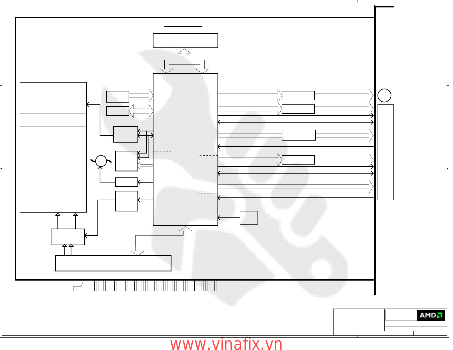
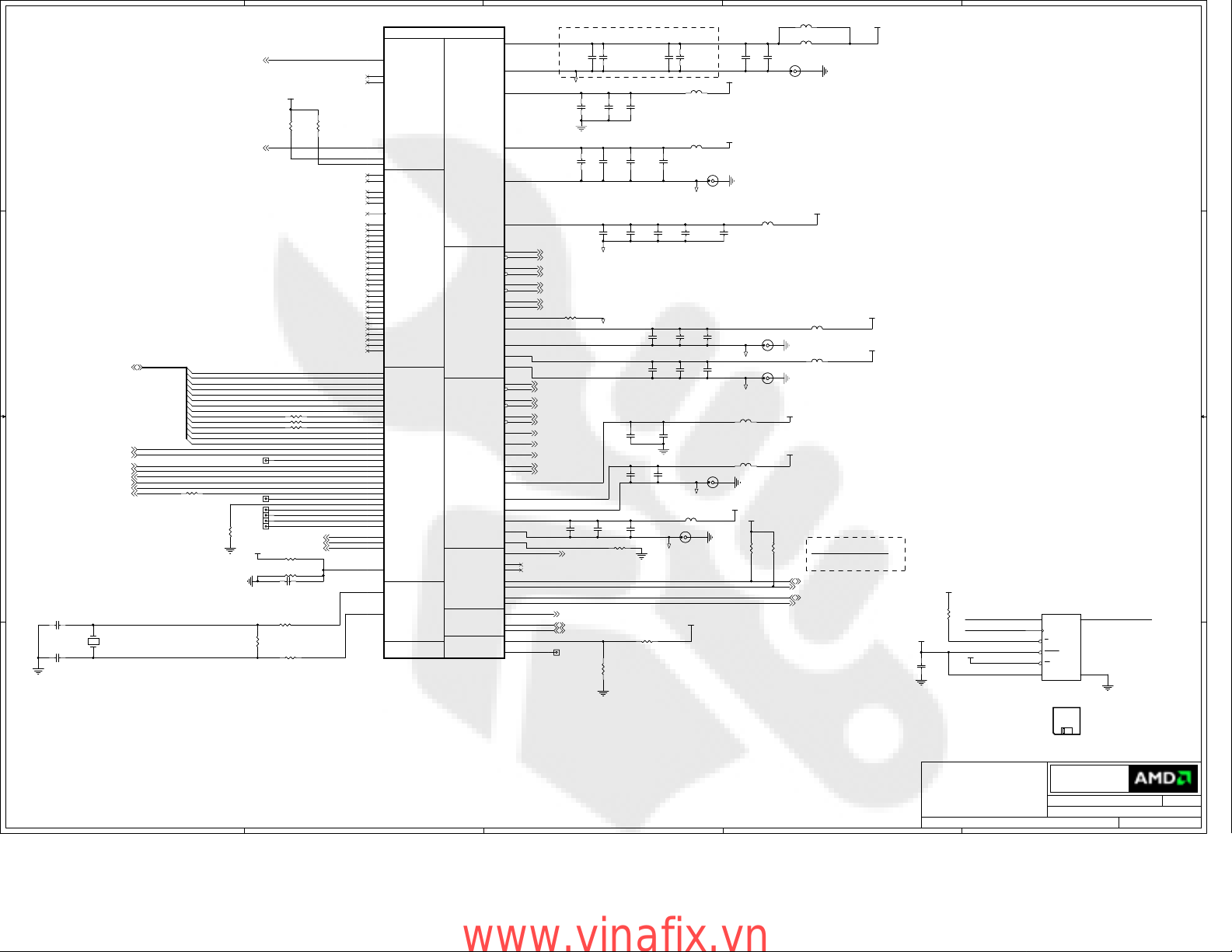
MEMORY CHANNEL A
D D
64bit DDR2 32M/16Mx16
MEM A0 MEM A1
POWER REGULATION
CFTb
GPIO0..7
GPIO9, 11..13
GPIO8..10
GPIO22
DDC2_CLK
DDC2_DATA
Internal
Temperature
Reader
D+/D-
TS_FDO
PWM Out
GPIO19
Fan Circuit
Settings
BIOS
Temperature
Sensor Output
FAN
Straps/
Switches
Flash ROM
VDDC
Voltage Control
External
Temperature
Reader
Critical Temp.
Fault Circuit
From +12V SMPS
ASIC Core:
ASIC Core I/O:
Memory:
From +12V LIN.REG.
+5V_VESA
C C
From +12V_BUS DIRECT
FAN
From +3.3V LIN.REG. to 1.8V/1.1V
Memory PLL:
PCIe:
I/O Level Shift:
PLL_Analog:
DVP:
DAC1:
DAC2:
TMDS2:
From +3.3V DIRECT
3.3V I/O:
B B
VDDC
VDDCI
MVDD, VDDR1, VDDRH
MPVDD
PCIE_VDDC, PCIE_VDDR, PCIE_PVDD
VDD_CT
DPLL_PVDD, DPLL_VDDC
VDDR4, VDDR5
AVDD, VDD1DI
A2VDD, VDD2DI, A2VDDQ
DPA/B_PVDD, DPA/B_VDDRDP/TMDS1:
T2PVDD, T2XVDDR
VDDR3
+PCIE_SOURCE
+12V_BUS+3.3V_BUS
DAC2
C
Y
COMP
CRT
H/VSync
DDC4
VO Filter
RGB Filter
VO
TMDS1
Data
Clock
HPD2
TMDS Termination
DAC1
RV620 ASIC
CRT
H/VSync
DDC3
RGB Filter
DMS-59 Connector
(2 singlelink DVI-I)
TMDS2
Data
(internal termination)
Clock
HPD1
XTALIN/OUT
Crystal
PCI-Express
Power Up/Down
Sequencing Circuit
+3.3V_BUS
+12V_BUS
PCI-Express Bus
RV620 B629 DDR2 6-Layer LP
REV 03
A A
CONFIDENTIAL & PROPRIETARY TO ADVANCED MICRO DEVICES INC.
CONFIDENTIAL & PROPRIETARY TO ADVANCED MICRO DEVICES INC.
CONFIDENTIAL & PROPRIETARY TO ADVANCED MICRO DEVICES INC.
© 2007 Advanced Micro Devices
© 2007 Advanced Micro Devices
© 2007 Advanced Micro Devices
This AMD Board schematic and design is the exclusive property of AMD,
This AMD Board schematic and design is the exclusive property of AMD,
This AMD Board schematic and design is the exclusive property of AMD,
and is provided only to entities under a non-disclosure agreement
and is provided only to entities under a non-disclosure agreement
and is provided only to entities under a non-disclosure agreement
with AMD for evaluation purposes. Further distribution or disclosure
with AMD for evaluation purposes. Further distribution or disclosure
with AMD for evaluation purposes. Further distribution or disclosure
is strictly prohibited. Use of this schematic and design for any purpose
is strictly prohibited. Use of this schematic and design for any purpose
is strictly prohibited. Use of this schematic and design for any purpose
other than evaluation requires a Board Technology License Agreement
other than evaluation requires a Board Technology License Agreement
other than evaluation requires a Board Technology License Agreement
with AMD. AMD makes no representations or warranties of any kind
with AMD. AMD makes no representations or warranties of any kind
with AMD. AMD makes no representations or warranties of any kind
regarding this schematic and design, including, not limited to,
regarding this schematic and design, including, not limited to,
regarding this schematic and design, including, not limited to,
any implied warranty of merchantibility or fitness for a particular
any implied warranty of merchantibility or fitness for a particular
any implied warranty of merchantibility or fitness for a particular
purpose, and disclaims responsibility forany consequences resulting
purpose, and disclaims responsibility forany consequences resulting
purpose, and disclaims responsibility forany consequences resulting
from use of the information included herein.
from use of the information included herein.
from use of the information included herein.
Title
Title
Title
RH RV620 - BLOCK DIAGRAM
RH RV620 - BLOCK DIAGRAM
5
4
3
2
RH RV620 - BLOCK DIAGRAM
Advanced Micro Devices Inc.
Advanced Micro Devices Inc.
Advanced Micro Devices Inc.
1 Commerce Valley Drive East
1 Commerce Valley Drive East
1 Commerce Valley Drive East
Markham, Ontario
Markham, Ontario
Markham, Ontario
Friday, April 25, 2008
Friday, April 25, 2008
Friday, April 25, 2008
Sheet
Sheet
Sheet
of
20 20
of
20 20
of
20 20
1
Doc No.
Doc No.
Doc No.
RevDate:
RevDate:
RevDate:
03
03
03
105-B629xx-00B
105-B629xx-00B
105-B629xx-00B
www.vinafix.vn
Page 3
8
7
6
5
4
3
2
1
TYPHOON
D D
TP30TP30
TP31TP31
TP6TP6
PETn0_GFXRn0(2)
PETp1_GFXRp1(2)
PETn1_GFXRn1(2)
PETp2_GFXRp2(2)
C C
+12V_BUS
C1
CAP CER 10UF 20% 16V X5R
10UFC110UF
(1206)1.8MM H MAX
+12V_BUS
+12V_BUS
C3
C3
C2
150nF_16V
150nF_16V
150nF_16VC2150nF_16V
LF CAP CER 150NF 10% 16V X7R (0603)
LF CAP CER 150NF 10% 16V X7R (0603)
+3.3V_BUS
CAP CER 10UF 10% 6.3V X5R
(0805)1.4MM MAX THICK
C4
+3.3V_BUS
10uFC410uF
C5
1uF_6.3VC51uF_6.3V
Place these caps last,
ideally as close to the bus
connector as possible
C6
1uF_6.3VC61uF_6.3V
C0
10nFC010nF
B B
PETn2_GFXRn2(2)
PETp3_GFXRp3(2)
PETn3_GFXRn3(2)
PETp4_GFXRp4(2)
PETn4_GFXRn4(2)
PETp5_GFXRp5(2)
PETn5_GFXRn5(2)
PETp6_GFXRp6(2)
PETn6_GFXRn6(2)
PETp7_GFXRp7(2)
PETn7_GFXRn7(2)
PETp8_GFXRp8(2)
PETn8_GFXRn8(2)
PETp9_GFXRp9(2)
PETn9_GFXRn9(2)
PETp10_GFXRp10(2)
PETn10_GFXRn10(2)
PETp11_GFXRp11(2)
PETn11_GFXRn11(2)
PETp12_GFXRp12(2)
PETn12_GFXRn12(2)
PETp13_GFXRp13(2)
PETn13_GFXRn13(2)
PETp14_GFXRp14(2)
PETn14_GFXRn14(2)
PETp15_GFXRp15(2)
PETn15_GFXRn15(2)
PRESENCE
PCI-EXPRESS EDGE CONNECTOR
+12V_BUS+3.3V_BUS +3.3V_BUS+12V_BUS
x16 PCIe
x16 PCIe
B1
+12V#B1
B2
+12V#B2
B3
+12V#B3
B4
SMCLK
SMDAT JTDI
JTRST#
B5
B6
B7
B8
B9
B10
B11
B12
B13
B14
B15
B16
B17
B18
B19
B20
B21
B22
B23
B24
B25
B26
B27
B28
B29
B30
B31
B32
B33
B34
B35
B36
B37
B38
B39
B40
B41
B42
B43
B44
B45
B46
B47
B48
B49
B50
B51
B52
B53
B54
B55
B56
B57
B58
B59
B60
B61
B62
B63
B64
B65
B66
B67
B68
B69
B70
B71
B72
B73
B74
B75
B76
B77
B78
B79
B80
B81
B82
GND#B4
SMCLK
SMDAT
GND#B7
+3.3V#B8
JTAG1
3.3Vaux
WAKE#
RSVD#B12
GND#B13
PETp0
PETn0
GND#B16
PRSNT2#B17
GND#B18
PETp1
PETn1
GND#B21
GND#B22
PETp2
PETn2
GND#B25
GND#B26
PETp3
PETn3
GND#B29
RSVD#B30
PRSNT2#B31
GND#B32
PETp4
PETn4
GND#B35
GND#B36
PETp5
PETn5
GND#B39
GND#B40
PETp6
PETn6
GND#B43
GND#B44
PETp7
PETn7
GND#B47
PRSNT2#B48
GND#B49
PETp8
PETn8
GND#B52
GND#B53
PETp9
PETn9
GND#B56
GND#B57
PETp10
PETn10
GND#B60
GND#B61
PETp11
PETn11
GND#B64
GND#B65
PETp12
PETn12
GND#B68
GND#B69
PETp13
PETn13
GND#B72
GND#B73
PETp14
PETn14
GND#B76
GND#B77
PETp15
PETn15
GND#B80
PRSNT2#B81
RSVD#B82
Mechanical Key
Mechanical Key
PRSNT1#A1
+12V#A2
+12V#A3
GND#A4
JTAG2
JTAG3
JTAG4
JTAG5
+3.3V#A9
+3.3V#A10
PERST#
GND#A12
REFCLK+
REFCLKGND#A15
PERp0
PERn0
GND#A18
RSVD#A19
GND#A20
PERp1
PERn1
GND#A23
GND#A24
PERp2
PERn2
GND#A27
GND#A28
PERp3
PERn3
GND#A31
RSVD#A32
RSVD#A33
GND#A34
PERp4
PERn4
GND#A37
GND#A38
PERp5
PERn5
GND#A41
GND#A42
PERp6
PERn6
GND#A45
GND#A46
PERp7
PERn7
GND#A49
RSVD#A50
GND#A51
PERp8
PERn8
GND#A54
GND#A55
PERp9
PERn9
GND#A58
GND#A59
PERp10
PERn10
GND#A62
GND#A63
PERp11
PERn11
GND#A66
GND#A67
PERp12
PERn12
GND#A70
GND#A71
PERp13
PERn13
GND#A74
GND#A75
PERp14
PERn14
GND#A78
GND#A79
PERp15
PERn15
GND#A82
MPCIE1
MPCIE1
A1
A2
A3
A4
A5
A6
A7
A8
A9
A10
A11
A12
A13
A14
A15
A16
A17
A18
A19
A20
A21
A22
A23
A24
A25
A26
A27
A28
A29
A30
A31
A32
A33
A34
A35
A36
A37
A38
A39
A40
A41
A42
A43
A44
A45
A46
A47
A48
A49
A50
A51
A52
A53
A54
A55
A56
A57
A58
A59
A60
A61
A62
A63
A64
A65
A66
A67
A68
A69
A70
A71
A72
A73
A74
A75
A76
A77
A78
A79
A80
A81
A82
PERp0
PERn0
PERp1
PERn1
PERp2
PERn2
PERp3
PERn3
PERp4
PERn4
PERp5
PERn5
PERp6
PERn6
PERp7
PERn7
PERp8
PERn8
PERp9
PERn9
PERp10
PERn10
PERp11
PERn11
PERp12
PERn12
PERp13
PERn13
PERp14
PERn14
PERp15
PERn15
PRESENCE
JTCK
JTDO
JTMS
C7
100nFC7100nF
C9
100nFC9100nF
C11
C11
100nF
100nF
C13
C13
100nF
100nF
C15
C15
100nF
100nF
C17
C17
100nF
100nF
C19
C19
100nF
100nF
C21
C21
100nF
100nF
C23
C23
100nF
100nF
C25
C25
100nF
100nF
C27
C27
100nF
100nF
C29
C29
100nF
100nF
C31
C31
100nF
100nF
C33
C33
100nF
100nF
C35
C35
100nF
100nF
C37
C37
100nF
100nF
C8
100nFC8100nF
C10
C10
100nF
100nF
C12
C12
100nF
100nF
C14
C14
100nF
100nF
C16
C16
100nF
100nF
C18
C18
100nF
100nF
C20
C20
100nF
100nF
C22
C22
100nF
100nF
C24
C24
100nF
100nF
C26
C26
100nF
100nF
C28
C28
100nF
100nF
C30
C30
100nF
100nF
C32
C32
100nF
100nF
C34
C34
100nF
100nF
C36
C36
100nF
100nF
C38
C38
100nF
100nF
TP1TP1
PCIE_REFCLKP (2)
PCIE_REFCLKN (2)PETp0_GFXRp0(2)
GFXTp0_PERp0 (2)
GFXTn0_PERn0 (2)
GFXTp1_PERp1 (2)
GFXTn1_PERn1 (2)
GFXTp2_PERp2 (2)
GFXTn2_PERn2 (2)
GFXTp3_PERp3 (2)
GFXTn3_PERn3 (2)
GFXTp4_PERp4 (2)
GFXTn4_PERn4 (2)
GFXTp5_PERp5 (2)
GFXTn5_PERn5 (2)
GFXTp6_PERp6 (2)
GFXTn6_PERn6 (2)
GFXTp7_PERp7 (2)
GFXTn7_PERn7 (2)
GFXTp8_PERp8 (2)
GFXTn8_PERn8 (2)
GFXTp9_PERp9 (2)
GFXTn9_PERn9 (2)
GFXTp10_PERp10 (2)
GFXTn10_PERn10 (2)
GFXTp11_PERp11 (2)
GFXTn11_PERn11 (2)
GFXTp12_PERp12 (2)
GFXTn12_PERn12 (2)
GFXTp13_PERp13 (2)
GFXTn13_PERn13 (2)
GFXTp14_PERp14 (2)
GFXTn14_PERn14 (2)
GFXTp15_PERp15 (2)
GFXTn15_PERn15 (2)
TP2TP2
TP3TP3 TP4TP4
PERST#
+3.3V
C39
C39
100nF
100nF
53
1
4
2
U5
U5
NC7SZ08P5X_NL
NC7SZ08P5X_NL
PERST#_buf (2)
SYMBOL LEGEND
DO NOT
DNI
INSTALL
ACTIVE
#
LOW
DIGITAL
Doc No.
Doc No.
Doc No.
1
GROUND
ANALOG
GROUND
RevDate:
RevDate:
RevDate:
03
03
03
105-B629xx-00B
105-B629xx-00B
105-B629xx-00B
A A
CONFIDENTIAL & PROPRIETARY TO ADVANCED MICRO DEVICES INC.
CONFIDENTIAL & PROPRIETARY TO ADVANCED MICRO DEVICES INC.
CONFIDENTIAL & PROPRIETARY TO ADVANCED MICRO DEVICES INC.
© 2007 Advanced Micro Devices
© 2007 Advanced Micro Devices
© 2007 Advanced Micro Devices
This AMD Board schematic and design is the exclusive property of AMD,
This AMD Board schematic and design is the exclusive property of AMD,
This AMD Board schematic and design is the exclusive property of AMD,
and is provided only to entities under a non-disclosure agreement
and is provided only to entities under a non-disclosure agreement
and is provided only to entities under a non-disclosure agreement
with AMD for evaluation purposes. Further distribution or disclosure
with AMD for evaluation purposes. Further distribution or disclosure
with AMD for evaluation purposes. Further distribution or disclosure
is strictly prohibited. Use of this schematic and design for any purpose
is strictly prohibited. Use of this schematic and design for any purpose
is strictly prohibited. Use of this schematic and design for any purpose
other than evaluation requires a Board Technology License Agreement
other than evaluation requires a Board Technology License Agreement
other than evaluation requires a Board Technology License Agreement
with AMD. AMD makes no representations or warranties of any kind
with AMD. AMD makes no representations or warranties of any kind
with AMD. AMD makes no representations or warranties of any kind
regarding this schematic and design, including, not limited to,
regarding this schematic and design, including, not limited to,
regarding this schematic and design, including, not limited to,
any implied warranty of merchantibility or fitness for a particular
any implied warranty of merchantibility or fitness for a particular
any implied warranty of merchantibility or fitness for a particular
purpose, and disclaims responsibility forany consequences resulting
purpose, and disclaims responsibility forany consequences resulting
purpose, and disclaims responsibility forany consequences resulting
from use of the information included herein.
from use of the information included herein.
from use of the information included herein.
Title
Title
Title
RH RV620 - PCI-E Edge Connector
RH RV620 - PCI-E Edge Connector
8
7
6
5
4
3
RH RV620 - PCI-E Edge Connector
2
Advanced Micro Devices Inc.
Advanced Micro Devices Inc.
Advanced Micro Devices Inc.
1 Commerce Valley Drive East
1 Commerce Valley Drive East
1 Commerce Valley Drive East
Markham, Ontario
Markham, Ontario
Markham, Ontario
Friday, April 25, 2008
Friday, April 25, 2008
Friday, April 25, 2008
Sheet
Sheet
Sheet
of
120
of
120
of
120
www.vinafix.vn
Page 4
5
D D
4
3
2
1
NOTE: some of the PCIE testpoints will
be available through via on traces.
PETp0_GFXRp0(1)
PETn0_GFXRn0(1)
PETp1_GFXRp1(1)
PETn1_GFXRn1(1)
PETp2_GFXRp2(1)
PETn2_GFXRn2(1)
PETp3_GFXRp3(1)
PETn3_GFXRn3(1)
PETp4_GFXRp4(1)
PETn4_GFXRn4(1)
PETp5_GFXRp5(1)
PETn5_GFXRn5(1)
PETp6_GFXRp6(1)
C C
B B
PETn6_GFXRn6(1)
PETp7_GFXRp7(1)
PETn7_GFXRn7(1)
PETp8_GFXRp8(1)
PETn8_GFXRn8(1)
PETp9_GFXRp9(1)
PETn9_GFXRn9(1)
PETp10_GFXRp10(1)
PETn10_GFXRn10(1)
PETp11_GFXRp11(1)
PETn11_GFXRn11(1)
PETp12_GFXRp12(1)
PETn12_GFXRn12(1)
PETp13_GFXRp13(1)
PETn13_GFXRn13(1)
PETp14_GFXRp14(1)
PETn14_GFXRn14(1)
PETp15_GFXRp15(1)
PETn15_GFXRn15(1)
PCIE_REFCLKP(1)
PCIE_REFCLKN(1)
DNI DNI
R13
R13
51R
51R
402 402
R14
R14
51R
51R
TP7TP7
TP8TP8
TP9TP9
TP10TP10
TP11TP11
TP12TP12
TP13TP13
TP14TP14
TP15TP15
TP16TP16
TP17TP17
TP18TP18
TP19TP19
TP20TP20
TP21TP21
TP22TP22
TP23TP23
TP24TP24
TP25TP25
TP26TP26
TP27TP27
TP28TP28
PERST#_buf(1)
AC30
AC31
AC29
AB29
AB31
AB30
AA31
AA30
AD29
AD30
AC28
AC27
AG25
W30
W31
W29
V29
V31
V30
U31
U30
P30
P31
P29
N29
N31
N30
M31
M30
K30
K31
K29
J29
J31
J30
H31
H30
U1A
U1A
PCIE_RX0P
PCIE_RX0N
PCIE_RX1P
PCIE_RX1N
PCIE_RX2P
PCIE_RX2N
PCIE_RX3P
PCIE_RX3N
PCIE_RX4P
PCIE_RX4N
PCIE_RX5P
PCIE_RX5N
PCIE_RX6P
PCIE_RX6N
PCIE_RX7P
PCIE_RX7N
PCIE_RX8P
PCIE_RX8N
PCIE_RX9P
PCIE_RX9N
PCIE_RX10P
PCIE_RX10N
PCIE_RX11P
PCIE_RX11N
PCIE_RX12P
PCIE_RX12N
PCIE_RX13P
PCIE_RX13N
PCIE_RX14P
PCIE_RX14N
PCIE_RX15P
PCIE_RX15N
Clock
Clock
PCIE_REFCLKP
PCIE_REFCLKN
NC_SMBCLK
NC_SMBDATA
PERSTB
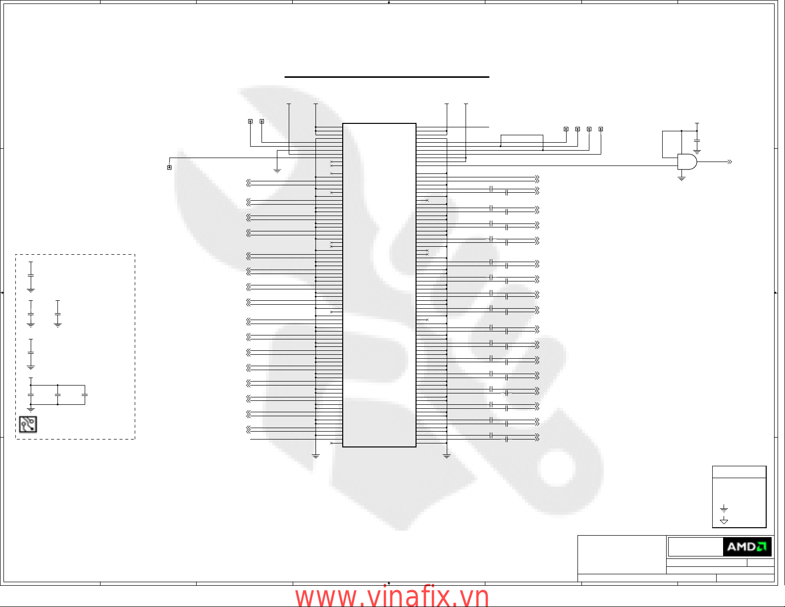
RV620 GL A11 RH
RV620 GL A11 RH
PART 1 OF 6
PART 1 OF 6
P
P
C
C
I
I
-
E
E
X
X
P
P
R
R
E
E
S
S
S
S
I
I
N
N
T
T
E
E
R
R
F
F
A
A
C
C
E
E
PCIE_TX0P
PCIE_TX0N
PCIE_TX1P
PCIE_TX1N
PCIE_TX2P
PCIE_TX2N
PCIE_TX3P
PCIE_TX3N
PCIE_TX4P
PCIE_TX4N
PCIE_TX5P
PCIE_TX5N
PCIE_TX6P
PCIE_TX6N
PCIE_TX7P
PCIE_TX7N
PCIE_TX8P
PCIE_TX8N
PCIE_TX9P
PCIE_TX9N
PCIE_TX10P
PCIE_TX10N
PCIE_TX11P
PCIE_TX11N
PCIE_TX12P
PCIE_TX12N
PCIE_TX13P
PCIE_TX13N
PCIE_TX14P
PCIE_TX14N
PCIE_TX15P
PCIE_TX15N
Calibration
Calibration
PCIE_CALRN
PCIE_CALRP
AA28
AA27
AA25
AA24
Y28
Y27
Y25
Y24
V28
V27
V25
V24
T28
T27
T25
T24
P28
P27
P25
P24
M28
M27
M25
M24
L28
L27
L25
L24
J28
J27
G28
G27
+1.1V
PCIE_CALRN
AF25
PCIE_CALRP
AE25
AE23
NC
402
R82.0K R82.0K
402
R91.27K R91.27K
GFXTp0_PERp0 (1)
GFXTn0_PERn0 (1)
GFXTp1_PERp1 (1)
GFXTn1_PERn1 (1)
GFXTp2_PERp2 (1)
GFXTn2_PERn2 (1)
GFXTp3_PERp3 (1)
GFXTn3_PERn3 (1)
GFXTp4_PERp4 (1)
GFXTn4_PERn4 (1)
GFXTp5_PERp5 (1)
GFXTn5_PERn5 (1)
GFXTp6_PERp6 (1)
GFXTn6_PERn6 (1)
GFXTp7_PERp7 (1)
GFXTn7_PERn7 (1)
GFXTp8_PERp8 (1)
GFXTn8_PERn8 (1)
GFXTp9_PERp9 (1)
GFXTn9_PERn9 (1)
GFXTp10_PERp10 (1)
GFXTn10_PERn10 (1)
GFXTp11_PERp11 (1)
GFXTn11_PERn11 (1)
GFXTp12_PERp12 (1)
GFXTn12_PERn12 (1)
GFXTp13_PERp13 (1)
GFXTn13_PERn13 (1)
GFXTp14_PERp14 (1)
GFXTn14_PERn14 (1)
GFXTp15_PERp15 (1)
GFXTn15_PERn15 (1)
For Tektronix LA only
Place close
to ASIC
A A
CONFIDENTIAL & PROPRIETARY TO ADVANCED MICRO DEVICES INC.
CONFIDENTIAL & PROPRIETARY TO ADVANCED MICRO DEVICES INC.
CONFIDENTIAL & PROPRIETARY TO ADVANCED MICRO DEVICES INC.
© 2007 Advanced Micro Devices
© 2007 Advanced Micro Devices
© 2007 Advanced Micro Devices
This AMD Board schematic and design is the exclusive property of AMD,
This AMD Board schematic and design is the exclusive property of AMD,
This AMD Board schematic and design is the exclusive property of AMD,
and is provided only to entities under a non-disclosure agreement
and is provided only to entities under a non-disclosure agreement
and is provided only to entities under a non-disclosure agreement
with AMD for evaluation purposes. Further distribution or disclosure
with AMD for evaluation purposes. Further distribution or disclosure
with AMD for evaluation purposes. Further distribution or disclosure
is strictly prohibited. Use of this schematic and design for any purpose
is strictly prohibited. Use of this schematic and design for any purpose
is strictly prohibited. Use of this schematic and design for any purpose
other than evaluation requires a Board Technology License Agreement
other than evaluation requires a Board Technology License Agreement
other than evaluation requires a Board Technology License Agreement
with AMD. AMD makes no representations or warranties of any kind
with AMD. AMD makes no representations or warranties of any kind
with AMD. AMD makes no representations or warranties of any kind
regarding this schematic and design, including, not limited to,
regarding this schematic and design, including, not limited to,
regarding this schematic and design, including, not limited to,
any implied warranty of merchantibility or fitness for a particular
any implied warranty of merchantibility or fitness for a particular
any implied warranty of merchantibility or fitness for a particular
purpose, and disclaims responsibility forany consequences resulting
purpose, and disclaims responsibility forany consequences resulting
purpose, and disclaims responsibility forany consequences resulting
from use of the information included herein.
from use of the information included herein.
from use of the information included herein.
Title
Title
Title
RH RV610 - ASIC PCIE Interface
RH RV610 - ASIC PCIE Interface
5
4
3
2
RH RV610 - ASIC PCIE Interface
Advanced Micro Devices Inc.
Advanced Micro Devices Inc.
Advanced Micro Devices Inc.
1 Commerce Valley Drive East
1 Commerce Valley Drive East
1 Commerce Valley Drive East
Markham, Ontario
Markham, Ontario
Markham, Ontario
Friday, April 25, 2008
Friday, April 25, 2008
Friday, April 25, 2008
Sheet
Sheet
Sheet
of
220
of
220
of
220
1
Doc No.
Doc No.
Doc No.
RevDate:
RevDate:
RevDate:
03
03
03
105-B629xx-00B
105-B629xx-00B
105-B629xx-00B
www.vinafix.vn
Page 5
5
PSYNC(13)
+3.3V
D D
R47
R47
4.7K
4.7K
DVALID(13)
C C
GPIO_[13..0](13)
GPIO_8
R30 33RR30 33R
GPIO_9
R31 33RR31 33R
GPIO_10
R32 33RR32 33R
HPD2(14)
C82
C82
6R8PF
6R8PF
PWRCNTL_0(11)
ThermINT(17)
GPIO_18(13)
CTFb(17)
PWRCNTL_1(11)
GPIO21_BB_EN(13)
GPIO_22(13)
R33 33RR33 33R
XTALIN_S XTALIN
GPIO_16 IS OUT ONLY
B B
2 1
C83
C83
Y82
Y82
6R8PF
6R8PF
27.000MHz_10PPM
27.000MHz_10PPM
A A
5
MR51KMR5
1K
+1.8V_D2
TP54TP54
TP50TP50
TP62TP62
TP61TP61
TP64TP64
TP63TP63
R43 221RR43 221R
R44 110RR44 110R
C46 100nFC46 100nF
R86 100RR86 100R
R841MR84
1M
R85 0RR85 0R
GENERICA(16)
GENERICB(13)
GENERICC(13)
PSYNC
R48
R48
4.7K
4.7K
DVALID
GPIO_0
GPIO_1
GPIO_2
GPIO_3
GPIO_4
GPIO_5
GPIO_6
GPIO_7
GPIO8_SO
GPIO9_SI
GPIO10_SCK
GPIO_11
GPIO_12
GPIO_13
GPIO_14
PWRCNTL_0
GPIO_16
GPIO_18
CTFb
PWRCNTL_1
GPIO21_BB_EN
GPIO22_CS
PCIE_CLK_REQb
JTAG_MODE
JTAG_TDI
JTAG_TCK
JTAG_TMS
JTAG_TDO
GENERICA
GENERICB
GENERICC
VREFG
XTALOUTXTALOUT_S
SDA
SCL
4
AE7
AH6
AG6
AD9
AA4
AA5
AK4
AL3
W3
W1
AA2
AA3
AB1
AB2
AB3
AC1
AC3
AD1
AD2
AD3
AF3
AG3
AH3
AG1
AH2
AH1
AJ3
AJ1
AJ2
AK2
AK3
AC11
AJ31
AJ30
4
U1B
U1B
V2
V1
Y1
Y2
Y3
Y4
V3
V4
V5
U3
U2
T4
T5
T7
T8
R1
R2
R3
P1
P3
N1
N2
P4
P7
P8
P5
V7
N3
Y5
M4
M5
M7
M8
L8
Y8
Y7
V8
RV620 GL A11 RH
RV620 GL A11 RH
PSYNC_NEW
GEN_D_HPD4
GEN_E
MISC/I2C
MISC/I2C
DVALID
SDA
SCL
DVPCNTL_MVP_0
DVPCNTL_MVP_1
DVPCNTL_0
DVPCNTL_1
DVPCNTL_2
DVPCLK
DVPDATA_0
DVPDATA_1
DVPDATA_2
DVPDATA_3
DVPDATA_4
DVPDATA_5
External
External
DVPDATA_6
TMDS
TMDS
DVPDATA_7
DVPDATA_8
DVPDATA_9
DVPDATA_10
DVPDATA_11
DVPDATA_12
DVPDATA_13
DVPDATA_14
DVPDATA_15
DVPDATA_16
DVPDATA_17
DVPDATA_18
DVPDATA_19
DVPDATA_20
DVPDATA_21
DVPDATA_22
DVPDATA_23
GPIO_0
GPIO_1
GPIO_2
General
General
GPIO_3
Purpose
Purpose
GPIO_4
I/O
I/O
GPIO_5
GPIO_6
GPIO_7_BLON
GPIO_8_ROMSO
GPIO_9_ROMSI
GPIO_10_ROMSCK
GPIO_11
GPIO_12
GPIO_13
GPIO_14_HPD2
GPIO_15_PWRCNTL0
GPIO_16_SSIN
GPIO_17_THERMAL_INT
GPIO_18_HPD3
GPIO_19_CTFB
GPIO_20_PWRCNTL1
GPIO_21_BB_EN
GPIO_22_ROMCSB
GPIO_23_CLKREQB
GPIO_24_JMODE
GPIO_25_TDI
GPIO_26_TCK
GPIO_27_TMS
GPIO_28_TDO
GENERICA
GENERICB
GENERICC
VREFG
XTALIN
XTAL
XTAL
XTALOUT
PART 2 OF 6
PART 2 OF 6
PLL Power
PLL Power
DAC / CRT
DAC / CRT
DAC2 (TV/CRT2)
DAC2 (TV/CRT2)
Monitor
Monitor
Interface
Interface
DDC3DATA_DP3_AUXN
DDC3CLK_DP3_AUXP
Thermal
Thermal
Test
Test
DPLL_PVDD
DPLL_PVSS
PCIE_PVDD
MPVDD
MPVSS
DPLL_VDDC
HSYNC
VSYNC
RSET
AVDD
AVSSQ
VDD1DI
VSS1DI
COMP
V2SYNC
H2SYNC
A2VDD
A2VDDQ
A2VSSQ
VDD2DI
VSS2DI
R2SET
HPD1
DDC1DATA
DDC1CLK
DDC2DATA
DDC2CLK
TS_FDO
DPLUS
DMINUS
TESTEN
PLLTEST
3
AH12
C72
C72
10uF_X6S
10uF_X6S
GND_PVSS
AG12
GND_PVSS
+PCIE_PVDD
AH31
C933
C933
C932
C932
1uF_6.3V
1uF_6.3V
10uF_X6S
10uF_X6S
+MPVDD
A9
C84
C84
10nF
GND_MPVSS
B9
+DPLL_VDDC
AE12
AL28
R
AK28
RB
AL27
G
AK27
GB
AL26
B
AK26
BB
AK29
AK30
RSET
AJ28
+AVDD
AL29
AH28
AJ27
AJ26
AL17
R2
AK17
R2B
AL15
G2
AK15
G2B
AL14
B2
AK14
B2B
AJ17
C
AJ15
Y
AJ14
AE16
AF16
+A2VDD
AH14
+A2VDDQ
AH16
AG16
+VDD2DI
AF18
AE18
AG14
R2SET
AA8
AJ29
AH29
AC5
AC4
AF4
AH4
AE14
AE5
AE4
TEST_EN
AH26
AD12
10nF
A_R_DAC1 (14)
A_RB_DAC1 (14)
A_G_DAC1 (14)
A_GB_DAC1 (14)
A_B_DAC1 (14)
A_BB_DAC1 (14)
A_HSYNC_DAC1 (13,14)
A_VSYNC_DAC1 (13,14)
R1030 499RR1030 499R
+VDD1DI
A_R_DAC2 (15)
A_RB_DAC2 (15)
A_G_DAC2 (15)
A_GB_DAC2 (15)
A_B_DAC2 (15)
A_BB_DAC2 (15)
DAC2_C (16)
DAC2_Y (16)
DAC2_COMP (16)
A_VSYNC_DAC2 (13,15)
A_HSYNC_DAC2 (13,15)
C2024
C2024
10nF
10nF
HPD1 (14)
TS_FDO (17)
GPU_DPLUS (17)
GPU_DMINUS (17)
TP42TP42
MC72
MC72
4.7uF_6.3V
4.7uF_6.3V
C931
C931
100nF
100nF
C85
C85
100nF
100nF
C64
C64
10nF
10nF
GND_PVSS
GND_AVSSQ
C2025
C2025
1uF_6.3V
1uF_6.3V
R2030 715RR2030 715R
MR71KMR7
1K
3
DNI DNI
C886
C886
10uF_X6S
10uF_X6S
C86
C86
C76
C76
1uF_6.3V
1uF_6.3V
1uF_6.3V
1uF_6.3V
GND_MPVSS
C60
C60
C61
C61
10nF
10nF
100nF
100nF
C1020
C1020
10nF
10nF
10V X7R
402 10%
C1023
C1023
10nF
10nF
C2032
C2032
C2031
C2031
1uF_6.3V
1uF_6.3V
100nF
100nF
C2021
C2021
C2022
C2022
100nF
100nF
1uF_6.3V
1uF_6.3V
C2026
C2026
NS2021NS_VIANS2021NS_VIA
4.7uF_6.3V
4.7uF_6.3V
GND_VSS2DI
R7 1KR7 1K
MC886
MC886
4.7uF_6.3V
4.7uF_6.3V
B931
B931
BLM15BD121SN1
BLM15BD121SN1
B67
B67
60R
60R
C62
C62
1uF_6.3V
1uF_6.3V
C1021
C1021
100nF
100nF
10V X5R
402 10%
C1024
C1024
100nF
100nF
NS2020NS_VIANS2020NS_VIA
GND_A2VSSQ
B885
B885
BLM15BD121SN1
BLM15BD121SN1
12
+3.3V
100nF
100nF
+1.8V_D2
+VDDC
NS64NS_VIA NS64NS_VIA
12
C1022
C1022
1uF_6.3V
1uF_6.3V
6.3V X5R
402 10%
C1025
C1025
1uF_6.3V
1uF_6.3V
12
+1.8V_D2
C71
C71
C63
C63
10uF_X6S
10uF_X6S
OVERLAP
+DPLL_PVDD
B993 1Kohm@100MHzB993 1Kohm@100MHz
B886
B886
BLM15BD121SN1
BLM15BD121SN1
C70
C70
10nF
10nF
B60
B60
BLM15BD121SN1
BLM15BD121SN1
NS1020NS_VIANS1020NS_VIA
12
GND_AVSSQ
NS1021NS_VIANS1021NS_VIA
12
GND_VSS1DI
+3.3V
B2030
B2030
120R_300mA
120R_300mA
Possible alternate 5150005600G
+1.8V_D2
B883
B883
BLM15BD121SN1
BLM15BD121SN1
+3.3V
R40
R40
R41
R41
4.7K
4.7K
4.7K
4.7K
2
12
POPULATE B993 IF +1.8V IS
CONNECTED TO +MVDD
NS70NS_VIA NS70NS_VIA
+1.1V
B882
B882
BLM15BD121SN1
BLM15BD121SN1
B884
B884
BLM15BD121SN1
BLM15BD121SN1
I2C DEVICE ADDRESSES ON DDC2
DEVICE
ADDRESS
LM63
0x98
I2C DAC
0xA0
DDC2_DATA (11,17)
DDC2_CLK (11,17)
DDC3_DATA (14)
DDC3_CLK (14)
2
+1.8V_D2
+1.8V_D2
+1.8V_D2
+3.3V
R46
R46
10K
10K
GPIO_10
+3.3V
GPIO_22
ROM_WP
+3.3V
C47
C47
100nF
100nF
CONFIDENTIAL & PROPRIETARY TO ADVANCED MICRO DEVICES INC.
CONFIDENTIAL & PROPRIETARY TO ADVANCED MICRO DEVICES INC.
CONFIDENTIAL & PROPRIETARY TO ADVANCED MICRO DEVICES INC.
© 2007 Advanced Micro Devices
© 2007 Advanced Micro Devices
© 2007 Advanced Micro Devices
This AMD Board schematic and design is the exclusive property of AMD,
This AMD Board schematic and design is the exclusive property of AMD,
This AMD Board schematic and design is the exclusive property of AMD,
and is provided only to entities under a non-disclosure agreement
and is provided only to entities under a non-disclosure agreement
and is provided only to entities under a non-disclosure agreement
with AMD for evaluation purposes. Further distribution or disclosure
with AMD for evaluation purposes. Further distribution or disclosure
with AMD for evaluation purposes. Further distribution or disclosure
is strictly prohibited. Use of this schematic and design for any purpose
is strictly prohibited. Use of this schematic and design for any purpose
is strictly prohibited. Use of this schematic and design for any purpose
other than evaluation requires a Board Technology License Agreement
other than evaluation requires a Board Technology License Agreement
other than evaluation requires a Board Technology License Agreement
with AMD. AMD makes no representations or warranties of any kind
with AMD. AMD makes no representations or warranties of any kind
with AMD. AMD makes no representations or warranties of any kind
regarding this schematic and design, including, not limited to,
regarding this schematic and design, including, not limited to,
regarding this schematic and design, including, not limited to,
any implied warranty of merchantibility or fitness for a particular
any implied warranty of merchantibility or fitness for a particular
any implied warranty of merchantibility or fitness for a particular
purpose, and disclaims responsibility forany consequences resulting
purpose, and disclaims responsibility forany consequences resulting
purpose, and disclaims responsibility forany consequences resulting
from use of the information included herein.
from use of the information included herein.
from use of the information included herein.
Title
Title
Title
RH RV620 - ASIC Main
RH RV620 - ASIC Main
RH RV620 - ASIC Main
U2
U2
5
D
6
C
1
S
7
HOLD
3
W
8
VCC
VSS
M25P05-AVNM6P
M25P05-AVNM6P
BIOS1
BIOS1
BIOS
BIOS
113-XXXXXX-XXX
113-XXXXXX-XXX
VIDEO BIOS
FIRMWARE
Advanced Micro Devices Inc.
Advanced Micro Devices Inc.
Advanced Micro Devices Inc.
1 Commerce Valley Drive East
1 Commerce Valley Drive East
1 Commerce Valley Drive East
Markham, Ontario
Markham, Ontario
Markham, Ontario
Friday, April 25, 2008
Friday, April 25, 2008
Friday, April 25, 2008
Sheet
Sheet
Sheet
320
320
320
1
GPIO_8GPIO_9
2
Q
4
RevDate:
RevDate:
RevDate:
03
03
of
of
of
Doc No.
Doc No.
Doc No.
1
03
105-B629xx-00B
105-B629xx-00B
105-B629xx-00B
www.vinafix.vn
Page 6
5
D D
+1.8V_D2
32
Q100
Q100
SI2304DS
SI2304DS
1
C119
C119
10uF_X6S
10uF_X6S
LVT_EN(11)
C C
+1.8V_D2
B889 BLM15BD121SN1B889 BLM15BD121SN1
1 2
C102
C102
10uF_X6S
10uF_X6S
NS100NS_VIA NS100NS_VIA
+1.8V_D2
B887
B887
BLM15BD121SN1
BLM15BD121SN1
NS110NS_VIA NS110NS_VIA
1 2
GND_DPAPVSS
B B
+1.1V
B888
B888
30R_1A
30R_1A
C113
C113
10uF_X6S
10uF_X6S
C117
C117
10uF_X6S
10uF_X6S
4.7uF_6.3V
4.7uF_6.3V
OVERLAP
4.7uF_6.3V
4.7uF_6.3V
MC113
MC113
MC117
MC117
C111
C111
1uF_6.3V
1uF_6.3V
C147
C147
1uF_6.3V
1uF_6.3V
OVERLAP
C106
C106
1uF_6.3V
1uF_6.3V
C101
C101
100nF
100nF
GND_T2PVSS
C110
C110
100nF
100nF
C114
C114
100nF
100nF
4
+DPAB_PVDD
+DPAB_VDDR
C105
C105
1uF_6.3V
1uF_6.3V
100nF
100nF
C100
C100
+LTVDD18
+DPAB_PVDD
GND_DPAPVSS
+DPAB_VDDR
AF20
AG20
AJ18
AH20
AF23
AF21
AL18
AJ22
AJ25
AK18
AK23
AK25
AJ21
AL23
AL25
AG18
AH18
AE11
AF11
AJ12
AJ13
AK13
AL13
AH11
AL12
AJ11
AK12
AL7
AK7
AF7
AG7
AH7
AJ7
AJ8
AH9
U1F
U1F
PART6OF6
PART6OF6
T2XVDDR_1
T2XVDDR_2
T2XVDDC_1
T2XVDDC_2
T2XVSSR_1
T2XVSSR_2
T2XVSSR_3
T2XVSSR_4
T2XVSSR_5
T2XVSSR_6
T2XVSSR_7
T2XVSSR_8
T2XVSSR_9
T2XVSSR_10
T2XVSSR_11
T2PVDD
T2PVSS
Integrated TMDP
Integrated TMDP
DPA_PVDD
DPB_PVDD
DPA_PVSS
DPB_PVSS
DPA_VDDR_1
DPA_VDDR_2
DPB_VDDR_2
DPB_VDDR_1
DPA_VSSR_1
DPA_VSSR_2
DPA_VSSR_3
DPA_VSSR_4
DPA_VSSR_5
DPB_VSSR_1
DPB_VSSR_2
DPB_VSSR_3
DPB_VSSR_4
DPB_VSSR_5
RV620 GL A11 RH
RV620 GL A11 RH
3
RSVD_7
Control
Control
RSVD
LVTM channel
LVTM channel
RSVD_1
RSVD_2
T2X4P
T2X4M
T2X5P
T2X5M
RSVD_4
RSVD_3
RSVD_6
RSVD_5
T2XCP
T2XCM
T2X0P
T2X0M
T2X1P
T2X1M
T2X2P
T2X2M
T2X3P
T2X3M
TXCM_DPA3N
TXCP_DPA3P
TX0M_DPA2N
TX0P_DPA2P
TX1M_DPA1N
TX1P_DPA1P
TX2M_DPA0N
TX2P_DPA0P
TXCM_DPB3N
TXCP_DPB3P
TX0M_DPB2N
TX0P_DPB2P
TX1M_DPB1N
TX1P_DPB1P
TX2M_DPB0N
TX2P_DPB0P
DDC4CLK_DP4_AUXP
DDC4DATA_DP4_AUXN
DP_CALR
AA7
AC6
AD21
AE21
AJ24
AJ23
AK24
AL24
AG21
AH21
AG23
AH23
AL19
AK19
AJ20
AJ19
AK20
AL20
AK21
AL21
AK22
AL22
AJ4
AJ5
AL5
AK5
AL6
AK6
AK8
AL8
AK9
AL9
AJ9
AJ10
AL10
AK10
AL11
AK11
AG9
AF9
AG11
DP_CALR
TjXCP
TjXCM
TjX0P
TjX0M
TjX1P
TjX1M
TjX2P
TjX2M
DPA_TXCM
DPA_TXCP
DPA_TX0M
DPA_TX0P
DPA_TX1M
DPA_TX1P
DPA_TX2M
DPA_TX2P
R153
R153
150R
150R
1%
Place close to ASIC
<7mm
DNI
R106 100RR106 100R
R100 100RR100 100R
R101 100RR101 100R
R102 100RR102 100R
DDC4_CLK (15)
DDC4_DATA (15)
2
TjXCP (14)
TjXCM (14)
TjX0P (14)
TjX0M (14)
TjX1P (14)
TjX1M (14)
TjX2P (14)
TjX2M (14)
Place close to Connector
C1120 100nF_6.3VC1120 100nF_6.3V
C1121 100nF_6.3VC1121 100nF_6.3V
C1112 100nF_6.3VC1112 100nF_6.3V
C1113 100nF_6.3VC1113 100nF_6.3V
C1114 100nF_6.3VC1114 100nF_6.3V
C1115 100nF_6.3VC1115 100nF_6.3V
C1116 100nF_6.3VC1116 100nF_6.3V
C1117 100nF_6.3VC1117 100nF_6.3V
R130 499RR130 499R
R122 499RR122 499R
R124 499RR124 499R
R126 499RR126 499R
RV620 - INSTALL C1112-C1117, C1120, C1121 100nF X7R;
1
TXCM (14)
R131 499RR131 499R
R123 499RR123 499R
R125 499RR125 499R
R127 499RR127 499R
DP_GND
LVT_EN(11)
1
TXCP (14)
TX0M (14)
TX0P (14)
TX1M (14)
TX1P (14)
TX2M (14)
TX2P (14)
DNI - FOR
Q110
Q110
SI2304DS
SI2304DS
STUDY ONLY
MR1100RMR110
0R
32
A A
CONFIDENTIAL & PROPRIETARY TO ADVANCED MICRO DEVICES INC.
CONFIDENTIAL & PROPRIETARY TO ADVANCED MICRO DEVICES INC.
CONFIDENTIAL & PROPRIETARY TO ADVANCED MICRO DEVICES INC.
© 2007 Advanced Micro Devices
© 2007 Advanced Micro Devices
© 2007 Advanced Micro Devices
This AMD Board schematic and design is the exclusive property of AMD,
This AMD Board schematic and design is the exclusive property of AMD,
This AMD Board schematic and design is the exclusive property of AMD,
and is provided only to entities under a non-disclosure agreement
and is provided only to entities under a non-disclosure agreement
and is provided only to entities under a non-disclosure agreement
with AMD for evaluation purposes. Further distribution or disclosure
with AMD for evaluation purposes. Further distribution or disclosure
with AMD for evaluation purposes. Further distribution or disclosure
is strictly prohibited. Use of this schematic and design for any purpose
is strictly prohibited. Use of this schematic and design for any purpose
is strictly prohibited. Use of this schematic and design for any purpose
other than evaluation requires a Board Technology License Agreement
other than evaluation requires a Board Technology License Agreement
other than evaluation requires a Board Technology License Agreement
with AMD. AMD makes no representations or warranties of any kind
with AMD. AMD makes no representations or warranties of any kind
with AMD. AMD makes no representations or warranties of any kind
regarding this schematic and design, including, not limited to,
regarding this schematic and design, including, not limited to,
regarding this schematic and design, including, not limited to,
any implied warranty of merchantibility or fitness for a particular
any implied warranty of merchantibility or fitness for a particular
any implied warranty of merchantibility or fitness for a particular
purpose, and disclaims responsibility forany consequences resulting
purpose, and disclaims responsibility forany consequences resulting
purpose, and disclaims responsibility forany consequences resulting
from use of the information included herein.
from use of the information included herein.
from use of the information included herein.
Title
Title
Title
RH RV620 - ASIC TMDP/LVTM Interface
RH RV620 - ASIC TMDP/LVTM Interface
5
4
3
2
RH RV620 - ASIC TMDP/LVTM Interface
Advanced Micro Devices Inc.
Advanced Micro Devices Inc.
Advanced Micro Devices Inc.
1 Commerce Valley Drive East
1 Commerce Valley Drive East
1 Commerce Valley Drive East
Markham, Ontario
Markham, Ontario
Markham, Ontario
Friday, April 25, 2008
Friday, April 25, 2008
Friday, April 25, 2008
Sheet
Sheet
Sheet
of
420
of
420
of
420
1
Doc No.
Doc No.
Doc No.
RevDate:
RevDate:
RevDate:
03
03
03
105-B629xx-00B
105-B629xx-00B
105-B629xx-00B
www.vinafix.vn
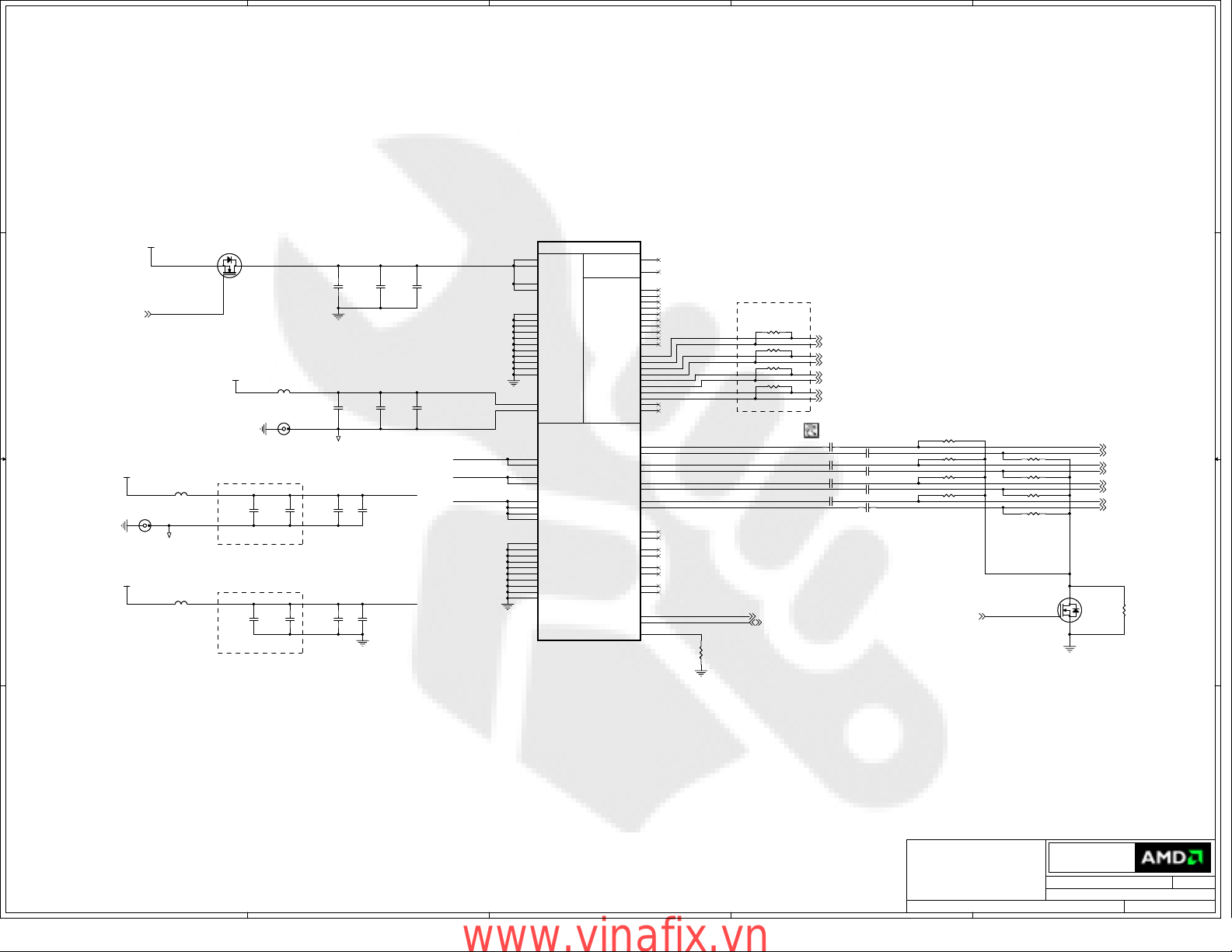
Page 7
5
D D
C C
B B
A A
5
4
U1E
U1E
AA26
PCIE_VSS_1
AA29
PCIE_VSS_2
AC26
PCIE_VSS_3
AD31
PCIE_VSS_4
AE29
PCIE_VSS_5
AE30
PCIE_VSS_6
AE31
PCIE_VSS_7
F28
PCIE_VSS_8
G26
PCIE_VSS_9
G29
PCIE_VSS_10
G30
PCIE_VSS_11
G31
PCIE_VSS_12
H29
PCIE_VSS_13
J25
PCIE_VSS_14
J26
PCIE_VSS_15
L26
PCIE_VSS_16
L29
PCIE_VSS_17
L30
PCIE_VSS_18
L31
PCIE_VSS_19
M26
PCIE_VSS_20
M29
PCIE_VSS_21
P26
PCIE_VSS_22
R29
PCIE_VSS_23
R30
PCIE_VSS_24
R31
PCIE_VSS_25
T26
PCIE_VSS_26
U29
PCIE_VSS_27
V26
PCIE_VSS_28
Y26
PCIE_VSS_29
Y29
PCIE_VSS_30
Y30
PCIE_VSS_31
Y31
PCIE_VSS_32
A13
VSS_1
A2
VSS_2
C18
VSS_3
A24
VSS_4
A30
VSS_5
AA1
VSS_6
AA11
VSS_7
AA14
VSS_8
AA17
VSS_9
AA20
VSS_10
AA6
VSS_11
AC2
VSS_12
AC7
VSS_13
AE3
VSS_15
AL4
VSS_16
AD14
VSS_17
AF12
VSS_18
AF14
VSS_19
AD16
VSS_20
AD18
VSS_21
AE6
VSS_22
AG2
VSS_23
AE9
VSS_24
AH25
VSS_25
AK1
VSS_26
AK31
VSS_27
AJ6
VSS_28
AL2
VSS_29
AL30
VSS_30
B1
VSS_31
C13
VSS_32
CORE GND
CORE GND
RV620 GL A11 RH
RV620 GL A11 RH
4
Part 5 of 6
Part 5 of 6
PCI-Express GND
PCI-Express GND
VSS_33
VSS_34
VSS_35
VSS_36
VSS_37
VSS_38
VSS_39
VSS_40
VSS_41
VSS_42
VSS_43
VSS_44
VSS_45
VSS_46
VSS_47
VSS_48
VSS_49
VSS_50
VSS_51
VSS_52
VSS_53
VSS_54
VSS_55
VSS_56
VSS_57
VSS_58
VSS_59
VSS_60
VSS_61
VSS_62
VSS_63
VSS_64
VSS_65
VSS_66
VSS_67
VSS_68
VSS_69
VSS_70
VSS_71
VSS_72
VSS_73
VSS_74
VSS_75
VSS_76
VSS_77
VSS_78
VSS_79
VSS_80
VSS_81
VSS_82
VSS_83
VSS_84
VSS_85
VSS_86
VSS_87
VSS_88
VSS_89
VSS_90
VSS_91
VSS_92
VSS_93
VSS_94
VSS_95
VSS_96
VSS_97
VSS_98
VSS_99
VSS_100
VSS_101
VSS_102
B25
J8
B5
D11
C17
C22
C27
D29
C3
C6
D3
D28
F29
D4
F11
F12
F14
F16
F18
F20
F21
F23
F25
F7
F9
G3
G6
H23
J3
J4
J6
K1
L12
L15
L18
L21
L6
M11
M14
M17
M20
M6
P12
P15
P18
P21
P6
AC21
R14
R17
R20
T6
U1
U12
U15
U18
U21
AE20
V14
V17
V20
P2
V6
W2
Y12
Y15
Y18
Y21
Y6
M9
3
3
2
CONFIDENTIAL & PROPRIETARY TO ADVANCED MICRO DEVICES INC.
CONFIDENTIAL & PROPRIETARY TO ADVANCED MICRO DEVICES INC.
CONFIDENTIAL & PROPRIETARY TO ADVANCED MICRO DEVICES INC.
© 2007 Advanced Micro Devices
© 2007 Advanced Micro Devices
© 2007 Advanced Micro Devices
This AMD Board schematic and design is the exclusive property of AMD,
This AMD Board schematic and design is the exclusive property of AMD,
This AMD Board schematic and design is the exclusive property of AMD,
and is provided only to entities under a non-disclosure agreement
and is provided only to entities under a non-disclosure agreement
and is provided only to entities under a non-disclosure agreement
with AMD for evaluation purposes. Further distribution or disclosure
with AMD for evaluation purposes. Further distribution or disclosure
with AMD for evaluation purposes. Further distribution or disclosure
is strictly prohibited. Use of this schematic and design for any purpose
is strictly prohibited. Use of this schematic and design for any purpose
is strictly prohibited. Use of this schematic and design for any purpose
other than evaluation requires a Board Technology License Agreement
other than evaluation requires a Board Technology License Agreement
other than evaluation requires a Board Technology License Agreement
with AMD. AMD makes no representations or warranties of any kind
with AMD. AMD makes no representations or warranties of any kind
with AMD. AMD makes no representations or warranties of any kind
regarding this schematic and design, including, not limited to,
regarding this schematic and design, including, not limited to,
regarding this schematic and design, including, not limited to,
any implied warranty of merchantibility or fitness for a particular
any implied warranty of merchantibility or fitness for a particular
any implied warranty of merchantibility or fitness for a particular
purpose, and disclaims responsibility forany consequences resulting
purpose, and disclaims responsibility forany consequences resulting
purpose, and disclaims responsibility forany consequences resulting
from use of the information included herein.
from use of the information included herein.
from use of the information included herein.
Title
Title
Title
RH RV620 - ASIC Ground
RH RV620 - ASIC Ground
RH RV620 - ASIC Ground
2
Advanced Micro Devices Inc.
Advanced Micro Devices Inc.
Advanced Micro Devices Inc.
1 Commerce Valley Drive East
1 Commerce Valley Drive East
1 Commerce Valley Drive East
Markham, Ontario
Markham, Ontario
Markham, Ontario
Friday, April 25, 2008
Friday, April 25, 2008
Friday, April 25, 2008
Sheet
Sheet
Sheet
of
520
of
520
of
520
1
Doc No.
Doc No.
Doc No.
1
RevDate:
RevDate:
RevDate:
03
03
03
105-B629xx-00B
105-B629xx-00B
105-B629xx-00B
www.vinafix.vn
Page 8

5
4
3
2
1
D D
C C
PLACE MVREF DIVIDERS
AND CAPS CLOSE TO ASIC
+MVDD
R291
R291
100R
100R
1%
C296
R292
+MVDD
R292
100R
100R
1%
R293
R293
100R
100R
1%
R294
R294
100R
100R
1%
B B
C295
C295
100nF
100nF
C297
C297
100nF
100nF
C296
10nF
10nF
C298
C298
10nF
10nF
M_MDA[63..0](8)
U1C
MVREFD_0
MVREFS_0
R296
R296
4.7K
4.7K
U1C
Part 3 of 6
M_MDA0
E29
M_MDA1
E30
M_MDA2
E31
M_MDA3
D31
M_MDA4
C29
M_MDA5
B29
M_MDA6
B30
M_MDA7
A29
M_MDA8
E26
M_MDA9
D26
M_MDA10
E25
M_MDA11
D25
M_MDA12
G23
M_MDA13
G21
M_MDA14
E21
M_MDA15
D21
M_MDA16
C28
M_MDA17
B28
M_MDA18
B27
M_MDA19
A27
M_MDA20
C25
M_MDA21
A25
M_MDA22
C24
M_MDA23
B24
M_MDA24
C23
M_MDA25
B23
M_MDA26
A23
M_MDA27
B22
M_MDA28
C20
M_MDA29
B20
M_MDA30
A20
M_MDA31
C19
M_MDA32
C8
M_MDA33
C7
M_MDA34
B7
M_MDA35
A7
M_MDA36
A5
M_MDA37
C4
M_MDA38
B4
M_MDA39
A3
M_MDA40
G9
M_MDA41
E9
M_MDA42
D9
M_MDA43
G7
M_MDA44
G5
M_MDA45
F5
M_MDA46
G4
M_MDA47
F4
M_MDA48
B3
M_MDA49
B2
M_MDA50
C2
M_MDA51
C1
M_MDA52
E3
M_MDA53
F3
M_MDA54
F2
M_MDA55
F1
M_MDA56
G2
M_MDA57
G1
M_MDA58
H3
M_MDA59
H2
M_MDA60
K2
M_MDA61
L3
M_MDA62
L2
M_MDA63
L1
F30
F31
TEST_MCLK
L5
TEST_YCLK
L7
MEMTEST DRAM_RST
R297
R297
R298
R298
4.7K
4.7K
243R
243R
DQ_0
DQ_1
DQ_2
DQ_3
DQ_4
DQ_5
DQ_6
DQ_7
DQ_8
DQ_9
DQ_10
DQ_11
DQ_12
DQ_13
DQ_14
DQ_15
DQ_16
DQ_17
DQ_18
DQ_19
DQ_20
DQ_21
DQ_22
DQ_23
DQ_24
DQ_25
DQ_26
DQ_27
DQ_28
DQ_29
DQ_30
DQ_31
DQ_32
DQ_33
DQ_34
DQ_35
DQ_36
DQ_37
DQ_38
DQ_39
DQ_40
DQ_41
DQ_42
DQ_43
DQ_44
DQ_45
DQ_46
DQ_47
DQ_48
DQ_49
DQ_50
DQ_51
DQ_52
DQ_53
DQ_54
DQ_55
DQ_56
DQ_57
DQ_58
DQ_59
DQ_60
DQ_61
DQ_62
DQ_63
MVREFD
MVREFS
TEST_MCLK
TEST_YCLK
J7
MEMTEST
RV620 GL A11 RH
RV620 GL A11 RH
Part 3 of 6
MEMORY
MEMORY
INTERFACE
INTERFACE
write strobe read strobe
write strobe read strobe
MA_10
MA_11
MA_BA0
MA_BA1
MA_A12
MA_BA2
DQMb_0
DQMb_1
DQMb_2
DQMb_3
DQMb_4
DQMb_5
DQMb_6
DQMb_7
QS_0B
QS_1B
QS_2B
QS_3B
QS_4B
QS_5B
QS_6B
QS_7B
ODT0
ODT1
CLK0b
CLK1b
RAS0b
RAS1b
CAS0b
CAS1b
CS0b_0
CS0b_1
CS1b_0
CS1b_1
CKE0
CKE1
WE0b
WE1b
DRAM_RST
MA_0
MA_1
MA_2
MA_3
MA_4
MA_5
MA_6
MA_7
MA_8
MA_9
QS_0
QS_1
QS_2
QS_3
QS_4
QS_5
QS_6
QS_7
CLK0
CLK1
M_MAA0
B14
M_MAA1
A14
M_MAA2
B13
M_MAA3
E14
M_MAA4
B17
M_MAA5
A17
M_MAA6
C15
M_MAA7
G16
M_MAA8
E16
M_MAA9
C14
M_MAA10
A12
M_MAA11
B12
M_MAA14
C12
M_MAA15
D14
M_MAA12
B15
M_MAA13
G14
M_DQMA#0
D30
M_DQMA#1
G25
M_DQMA#2
C26
M_DQMA#3
C21
M_DQMA#4
C5
M_DQMA#5
D6
M_DQMA#6
D2
M_DQMA#7
K3
M_QSA0
C30
M_QSA1
D23
M_QSA2
B26
M_QSA3
B21
M_QSA4
B6
M_QSA5
E7
M_QSA6
E2
M_QSA7
J2
C31
E23
A26
A21
A6
D7
E1
J1
E20
C11
A18
CLKA0 (8)
A11
CLKA1 (8)
B18
CLKA#0 (8)
B11
CLKA#1 (8)
G20
RASA#0 (8)
D12
RASA#1 (8)
D20
CASA#0 (8)
E12
CASA#1 (8)
E18
CSA#0_0 (8)
G18
G11
CSA#1_0 (8)
E11
D18
CKEA0 (8)
G12
CKEA1 (8)
D16
WEA#0 (8)
C10
WEA#1 (8)
J5
ODT (8)
+MVDD
R295
R295
2.0K
2.0K
DNI
MR295
MR295
4.7K
4.7K
M_MAA[15..0] (8)
M_DQMA#[7..0] (8)
M_QSA[7..0] (8)
Overlap
A A
5
DIVIDER RESISTORS DDR2 GDDR3
MVREF TO 1.8V
MVREF TO GND
40.2R100R
100R100R
CONFIDENTIAL & PROPRIETARY TO ADVANCED MICRO DEVICES INC.
CONFIDENTIAL & PROPRIETARY TO ADVANCED MICRO DEVICES INC.
CONFIDENTIAL & PROPRIETARY TO ADVANCED MICRO DEVICES INC.
© 2007 Advanced Micro Devices
© 2007 Advanced Micro Devices
© 2007 Advanced Micro Devices
This AMD Board schematic and design is the exclusive property of AMD,
This AMD Board schematic and design is the exclusive property of AMD,
This AMD Board schematic and design is the exclusive property of AMD,
and is provided only to entities under a non-disclosure agreement
and is provided only to entities under a non-disclosure agreement
and is provided only to entities under a non-disclosure agreement
with AMD for evaluation purposes. Further distribution or disclosure
with AMD for evaluation purposes. Further distribution or disclosure
with AMD for evaluation purposes. Further distribution or disclosure
is strictly prohibited. Use of this schematic and design for any purpose
is strictly prohibited. Use of this schematic and design for any purpose
is strictly prohibited. Use of this schematic and design for any purpose
other than evaluation requires a Board Technology License Agreement
other than evaluation requires a Board Technology License Agreement
other than evaluation requires a Board Technology License Agreement
with AMD. AMD makes no representations or warranties of any kind
with AMD. AMD makes no representations or warranties of any kind
with AMD. AMD makes no representations or warranties of any kind
regarding this schematic and design, including, not limited to,
regarding this schematic and design, including, not limited to,
regarding this schematic and design, including, not limited to,
any implied warranty of merchantibility or fitness for a particular
any implied warranty of merchantibility or fitness for a particular
any implied warranty of merchantibility or fitness for a particular
purpose, and disclaims responsibility forany consequences resulting
purpose, and disclaims responsibility forany consequences resulting
purpose, and disclaims responsibility forany consequences resulting
from use of the information included herein.
from use of the information included herein.
from use of the information included herein.
Title
Title
Title
RH RV620 - ASIC Memory Interface
RH RV620 - ASIC Memory Interface
4
3
2
RH RV620 - ASIC Memory Interface
Advanced Micro Devices Inc.
Advanced Micro Devices Inc.
Advanced Micro Devices Inc.
1 Commerce Valley Drive East
1 Commerce Valley Drive East
1 Commerce Valley Drive East
Markham, Ontario
Markham, Ontario
Markham, Ontario
Friday, April 25, 2008
Friday, April 25, 2008
Friday, April 25, 2008
Sheet
Sheet
Sheet
of
620
of
620
of
620
1
Doc No.
Doc No.
Doc No.
RevDate:
RevDate:
RevDate:
03
03
03
105-B629xx-00B
105-B629xx-00B
105-B629xx-00B
www.vinafix.vn
Page 9

5
D D
C134
C134
10uF_X6S
10uF_X6S
Recommended caps:
(see BOM for qualified values/vendors)
10uF , X6S, 10%, 0805, 6.3V, 1.4MM MAX THICK
1uF, X6S, 10%, 0402, 6.3V
100nF, X7R, 10%, 0402
10nF , X7R, 10%, 0402
C C
B B
C135
C135
10uF_X6S
10uF_X6S
+MVDD
C136
C136
10uF_X6S
10uF_X6S
C124
C124
C125
C125
10nF
10nF
10nF
10nF
C137
C137
C138
C138
10uF_X6S
10uF_X6S
1uF_6.3V
1uF_6.3V
+MVDD
B120 BLM15BD121SN1B120 BLM15BD121SN1
B121 BLM15BD121SN1B121 BLM15BD121SN1
NS121 NS_VIANS121 NS_VIA
C126
C126
10nF
10nF
C139
C139
1uF_6.3V
1uF_6.3V
C120
C120
1uF_6.3V
1uF_6.3V
12
GND_VSSRH0
+1.8V_D2
C127
C127
10nF
10nF
C140
C140
1uF_6.3V
1uF_6.3V
1uF_6.3V
1uF_6.3V
C128
C128
C129
C129
10nF
10nF
100nF
100nF
C141
C141
C142
C142
1uF_6.3V
1uF_6.3V
1uF_6.3V
1uF_6.3V
B70 BLM15BD121SN1B70 BLM15BD121SN1
+3.3V
+3.3V
C121
C121
NS122 NS_VIANS122 NS_VIA
12
GND_VSSRH1
1uF_6.3V
1uF_6.3V
C123
C123
C68
C68
10uF_X6S
10uF_X6S
C91
C91
1uF_6.3V
1uF_6.3V
C95
C95
1uF_6.3V
1uF_6.3V
C130
C130
100nF
100nF
C143
C143
1uF_6.3V
1uF_6.3V
1uF_6.3V
1uF_6.3V
C122
C122
C69
C69
100nF
100nF
C131
C131
100nF
100nF
C144
C144
1uF_6.3V
1uF_6.3V
C92
C92
1uF_6.3V
1uF_6.3V
C97
C97
100nF
100nF
4
C78
C78
1uF_6.3V
1uF_6.3V
C132
C132
100nF
100nF
C145
C145
100nF
100nF
C93
C93
100nF
100nF
C96
C96
1uF_6.3V
1uF_6.3V
+VDDC
C133
C133
100nF
100nF
C146
C146
100nF
100nF
C79
C79
1uF_6.3V
1uF_6.3V
C99
C99
100nF
100nF
C98
C98
100nF
100nF
+VDDRH1
+VDDRH2
GND_VSSRH1
GND_VSSRH0
+VDD_CT
C59
C59
100nF
100nF
AC18
AC16
AC14
AC12
AD11
AH30
A15
A22
A28
A4
A8
B8
C9
D1
H1
H11
H12
H14
H16
H18
H20
H21
B31
M1
AA9
Y9
V9
T9
J11
J20
J21
L9
AF1
AF2
AE1
AE2
M2
M3
L4
A10
A19
B10
B19
V11
U11
R11
P11
U1D
U1D
VDDR1_1
VDDR1_2
VDDR1_3
VDDR1_4
VDDR1_5
VDDR1_6
VDDR1_7
VDDR1_8
VDDR1_9
VDDR1_10
VDDR1_11
VDDR1_12
VDDR1_13
VDDR1_14
VDDR1_15
VDDR1_16
VDDR1_17
VDDR1_18
VDD_CT_1
VDD_CT_2
VDD_CT_3
VDD_CT_4
VDD_CT_5
VDD_CT_6
VDD_CT_7
VDD_CT_8
VDDR3_1
VDDR3_2
VDDR3_3
VDDR3_4
VDDR4_1
VDDR4_2
VDDR5_1
VDDR5_2
NC_1
NC_2
NC_3
NC_4
NC_5
VDDRH_1
VDDRH_2
VSSRH_1
VSSRH_2
BBN_1
BBN_2
BBP_1
BBP_2
RV620 GL A11 RH
RV620 GL A11 RH
Clock
Clock
I/O
I/O
PART 4 OF 6
PART 4 OF 6
P
P
O
O
I/O Internal
I/O Internal
W
W
E
E
R
R
Memory
Memory
Memory I/O
Memory I/O
Back Bias
Back Bias
3
PCIE_VDDR_1
PCIE_VDDR_2
PCIE_VDDR_3
PCIE_VDDR_4
PCIE_VDDR_5
PCIE_VDDR_6
PCIE_VDDR_7
PCIE_VDDR_8
PCIE_VDDC_1
PCIE_VDDC_2
PCIE_VDDC_3
PCIE_VDDC_4
PCIE_VDDC_5
PCIE_VDDC_6
PCIE_VDDC_7
PCIE_VDDC_8
PCIE_VDDC_9
PCIE_VDDC_10
PCIE_VDDC_11
PCI-Express
PCI-Express
PCIE_VDDC_12
VDDC_1
VDDC_2
VDDC_3
VDDC_4
VDDC_5
VDDC_6
VDDC_7
VDDC_8
VDDC_9
VDDC_10
VDDC_11
VDDC_12
VDDC_13
VDDC_14
VDDC_15
VDDC_16
Core
Core
VDDC_17
VDDC_18
VDDC_19
VDDC_20
VDDC_21
VDDC_22
VDDC_23
VDDC_24
VDDC_25
VDDC_26
VDDC_27
VDDC_28
VDDC_29
VDDC_30
VDDC_31
VDDC_32
VDDC_33
VDDCI_1
VDDCI_2
VDDCI_3
VDDCI_4
AF30
AF31
AF29
AF27
AF28
AG29
AG30
AG31
AA23
AC24
AC25
AE26
AE27
AE28
L23
M23
P23
T23
V23
Y23
L11
L14
L17
L20
M12
M15
M18
M21
AC20
P14
P17
P20
R12
R15
R18
R21
AD20
U14
U17
U20
V12
V15
V18
V21
Y11
Y14
Y17
Y20
AA12
AA15
AA18
AA21
P9
J12
J14
J16
J18
+VDDCI
C900
C900
1uF_6.3V
1uF_6.3V
C920
C920
1uF_6.3V
1uF_6.3V
C161
C161
1uF_6.3V
1uF_6.3V
C171
C171
1uF_6.3V
1uF_6.3V
C74
C74
100nF
100nF
C901
C901
1uF_6.3V
1uF_6.3V
C921
C921
1uF_6.3V
1uF_6.3V
C162
C162
1uF_6.3V
1uF_6.3V
C75
C75
1uF_6.3V
1uF_6.3V
C902
C902
1uF_6.3V
1uF_6.3V
C173
C173
1uF_6.3V
1uF_6.3V
C922
C922
1uF_6.3V
1uF_6.3V
1uF_6.3V
1uF_6.3V
C903
C903
1uF_6.3V
1uF_6.3V
C163
C163
1uF_6.3V
1uF_6.3V
C73
C73
C174
C174
1uF_6.3V
1uF_6.3V
C923
C923
1uF_6.3V
1uF_6.3V
C904
C904
10uF_X6S
10uF_X6S
C167
C167
1uF_6.3V
1uF_6.3V
C175
C175
1uF_6.3V
1uF_6.3V
C77
C77
10uF_X6S
10uF_X6S
2
C905
C905
10nF
10nF
C924
C924
1uF_6.3V
1uF_6.3V
B78 220R_2AB78 220R_2A
MR78 0RMR78 0R
+1.8V_D2
C925
C925
1uF_6.3V
1uF_6.3V
C168
C168
1uF_6.3V
1uF_6.3V
C176
C176
1uF_6.3V
1uF_6.3V
Overlap
C906
C906
100nF
100nF
C169
C169
1uF_6.3V
1uF_6.3V
C177
C177
1uF_6.3V
1uF_6.3V
C927
C927
1uF_6.3V
1uF_6.3V
C928
C928
1uF_6.3V
1uF_6.3V
C181
C181
10uF_X6S
10uF_X6S
C178
C178
1uF_6.3V
1uF_6.3V
+VDDC
+1.1V
C926
C926
10uF_X6S
10uF_X6S
C182
C182
10uF_X6S
10uF_X6S
C179
C179
1uF_6.3V
1uF_6.3V
C183
C183
10uF_X6S
10uF_X6S
C180
C180
1uF_6.3V
1uF_6.3V
1
+VDDC
C184
C184
10uF_X6S
10uF_X6S
C193
C193
100nF
100nF
A A
CONFIDENTIAL & PROPRIETARY TO ADVANCED MICRO DEVICES INC.
CONFIDENTIAL & PROPRIETARY TO ADVANCED MICRO DEVICES INC.
CONFIDENTIAL & PROPRIETARY TO ADVANCED MICRO DEVICES INC.
© 2007 Advanced Micro Devices
© 2007 Advanced Micro Devices
© 2007 Advanced Micro Devices
This AMD Board schematic and design is the exclusive property of AMD,
This AMD Board schematic and design is the exclusive property of AMD,
This AMD Board schematic and design is the exclusive property of AMD,
and is provided only to entities under a non-disclosure agreement
and is provided only to entities under a non-disclosure agreement
and is provided only to entities under a non-disclosure agreement
with AMD for evaluation purposes. Further distribution or disclosure
with AMD for evaluation purposes. Further distribution or disclosure
with AMD for evaluation purposes. Further distribution or disclosure
is strictly prohibited. Use of this schematic and design for any purpose
is strictly prohibited. Use of this schematic and design for any purpose
is strictly prohibited. Use of this schematic and design for any purpose
other than evaluation requires a Board Technology License Agreement
other than evaluation requires a Board Technology License Agreement
other than evaluation requires a Board Technology License Agreement
with AMD. AMD makes no representations or warranties of any kind
with AMD. AMD makes no representations or warranties of any kind
with AMD. AMD makes no representations or warranties of any kind
regarding this schematic and design, including, not limited to,
regarding this schematic and design, including, not limited to,
regarding this schematic and design, including, not limited to,
any implied warranty of merchantibility or fitness for a particular
any implied warranty of merchantibility or fitness for a particular
any implied warranty of merchantibility or fitness for a particular
purpose, and disclaims responsibility forany consequences resulting
purpose, and disclaims responsibility forany consequences resulting
purpose, and disclaims responsibility forany consequences resulting
from use of the information included herein.
from use of the information included herein.
from use of the information included herein.
Title
Title
Title
RH RV620 - ASIC Power
RH RV620 - ASIC Power
5
4
3
2
RH RV620 - ASIC Power
Advanced Micro Devices Inc.
Advanced Micro Devices Inc.
Advanced Micro Devices Inc.
1 Commerce Valley Drive East
1 Commerce Valley Drive East
1 Commerce Valley Drive East
Markham, Ontario
Markham, Ontario
Markham, Ontario
Friday, April 25, 2008
Friday, April 25, 2008
Friday, April 25, 2008
Sheet
Sheet
Sheet
of
720
of
720
of
720
1
Doc No.
Doc No.
Doc No.
RevDate:
RevDate:
RevDate:
03
03
03
105-B629xx-00B
105-B629xx-00B
105-B629xx-00B
www.vinafix.vn
Page 10

8
7
6
5
4
3
2
1
CHANNEL A: RANK 0 256MB DDR2
M_DQMA#[7..0](6)
D D
M_MDA[63..0](6)
M_MAA[15..0](6)
M_MAA[15..0](6)
C C
VREF_A0
+MVDD +MVDD +MVDD
R201
R201
4.99K
4.99K
R202
B B
R202
4.99K
4.99K
M_DQMA#0
M_DQMA#1
M_DQMA#2
M_DQMA#3
M_DQMA#4
M_DQMA#5
M_DQMA#6
M_DQMA#7
M_MAA14
L2
M_MAA15
L3
M_MAA12
R2
M_MAA11
P7
M_MAA10
M2
M_MAA9
P3
M_MAA8
P8
M_MAA7
P2
M_MAA6
N7
M_MAA5
N3
M_MAA4
N8
M_MAA3
N2
M_MAA2
M7
M_MAA1
M3
M_MAA0
M8
M_MAA13
TP200TP200
K8
CLKA#0(6)
J8
CLKA0(6)
K2
CKEA0(6)
CSA#0_0(6)
ODT(6) ODT(6) ODT(6) ODT(6)
R211 10RR211 10R
R212 10RR212 10R
VREF_U20
C413
C413
100nF
100nF
L8
WEA#0(6)
K7
RASA#0(6)
L7
CASA#0(6)
M_DQMA#2
F3
M_DQMA#3 M_DQMA#7
B3
K9
M_QSA2
F7
E8
M_QSA3
B7
A8
J2
A2
E2
L1
R3
R7
R8
U201
U201
BA0
BA1
A12
A11
A10/AP
A9
A8
A7
A6
A5
A4
A3
A2
A1
A0
CK
CK
CKE
CS
WEK3VDDQ10
RAS
CAS
LDM
UDM
ODT
LDQS
LDQS
UDQS
UDQS
VREF
VSSQ10
NC#A2
NC#E2
NC#L1
NC#R3
NC#R7
NC#R8
HY5PS561621F-25
HY5PS561621F-25
M_QSA[7..0](6)
DQ15
DQ14
DQ13
DQ12
DQ11
DQ10
VDDQ1
VDDQ2
VDDQ3
VDDQ4
VDDQ5
VDDQ6
VDDQ7
VDDQ8
VDDQ9
VDD1
VDD2
VDD3
VDD4
VDD5
VDDL
VSSDL
VSSQ1
VSSQ2
VSSQ3
VSSQ4
VSSQ5
VSSQ6
VSSQ7
VSSQ8
VSSQ9
VSS1
VSS2
VSS3
VSS4
VSS5
M_QSA0
M_QSA1
M_QSA2
M_QSA3
M_QSA4
M_QSA5
M_QSA6
M_QSA7
U204
U203
U202
U202
L2
BA0
L3
BA1
R2
A12
P7
A11
M2
A10/AP
P3
A9
P8
A8
P2
A7
N7
A6
N3
A5
N8
A4
N2
A3
M7
A2
M3
A1
M8
A0
K8
CK
J8
CK
K2
CKE
L8
CS
WEK3VDDQ10
K7
RAS
L7
CAS
F3
LDM
B3
UDM
K9
ODT
F7
LDQS
E8
LDQS
B7
UDQS
A8
UDQS
J2
VREF
A2
NC#A2
E2
NC#E2
L1
NC#L1
R3
NC#R3
R7
NC#R7
R8
NC#R8
HY5PS561621F-25
HY5PS561621F-25
DQ15
DQ14
DQ13
DQ12
DQ11
DQ10
VDDQ1
VDDQ2
VDDQ3
VDDQ4
VDDQ5
VDDQ6
VDDQ7
VDDQ8
VDDQ9
VDD1
VDD2
VDD3
VDD4
VDD5
VDDL
VSSDL
VSSQ1
VSSQ2
VSSQ3
VSSQ4
VSSQ5
VSSQ6
VSSQ7
VSSQ8
VSSQ9
VSSQ10
VSS1
VSS2
VSS3
VSS4
VSS5
M_MDA14
B9
M_MDA9
B1
M_MDA13
D9
M_MDA8
D1
M_MDA10
D3
M_MDA12
D7
M_MDA11
C2
DQ9
C8
DQ8
M_MDA6
F9
DQ7
M_MDA3
F1
DQ6
M_MDA4
H9
DQ5
M_MDA1
H1
DQ4
M_MDA2
H3
DQ3
M_MDA7
H7
DQ2
M_MDA0
G2
DQ1
M_MDA5
G8
DQ0
A9
C1
C3
C7
C9
E9
G1
G3
G7
G9
A1
E1
J9
M9
R1
VDDL_U21
J1
J7
C436
C436
100nF
100nF
A7
B2
B8
D2
D8
E7
F2
F8
H2
H8
A3
E3
J3
N1
P9
C437
C437
1uF_6.3V
1uF_6.3V
+MVDD
+MVDD
VREF_A1
R213 10RR213 10R
R214 10RR214 10R
R203
R203
4.99K
4.99K
VREF_U21
R204
R204
4.99K
4.99K
M_MAA14
M_MAA15
M_MAA12
M_MAA11
M_MAA10
M_MAA9
M_MAA8
M_MAA7
M_MAA6
M_MAA5
M_MAA4
M_MAA3
M_MAA2
M_MAA1
M_MAA0
CLKA#0(6)
CLKA0(6)
CKEA0(6)
CSA#0_0(6)
WEA#0(6)
RASA#0(6)
CASA#0(6)
M_DQMA#0
M_DQMA#1
M_QSA0
M_QSA1
C438
C438
100nF
100nF
M_MDA27
B9
M_MDA30
B1
M_MDA24
D9
M_MDA29
D1
M_MDA31
D3
M_MDA26
D7
M_MDA28
C2
DQ9
M_MDA25
C8
DQ8
M_MDA18
F9
DQ7
M_MDA21
F1
DQ6
M_MDA17
H9
DQ5
M_MDA22
H1
DQ4
M_MDA23
H3
DQ3
M_MDA16
H7
DQ2
M_MDA20
G2
DQ1
M_MDA19
G8
DQ0
A9
C1
C3
C7
C9
E9
G1
G3
G7
G9
A1
E1
J9
M9
R1
J1
J7
A7
B2
B8
D2
D8
E7
F2
F8
H2
H8
A3
E3
J3
N1
P9
VDDL_U20
C411
C411
100nF
100nF
C412
C412
1uF_6.3V
1uF_6.3V
+MVDD
+MVDD
VREF_A0
R215 10RR215 10R
R216 10RR216 10R
R205
R205
4.99K
4.99K
VREF_U22
R206
R206
4.99K
4.99K
M_MAA14
M_MAA15
M_MAA12
M_MAA11
M_MAA10
M_MAA9
M_MAA8
M_MAA7
M_MAA6
M_MAA5
M_MAA4
M_MAA3
M_MAA2
M_MAA1
M_MAA0
CLKA#1(6)
CLKA1(6)
CKEA1(6)
CSA#1_0(6)
WEA#1(6)
RASA#1(6)
CASA#1(6)
M_DQMA#6
M_QSA6
M_QSA7
C463
C463
100nF
100nF
U203
L2
BA0
L3
BA1
R2
A12
P7
A11
M2
A10/AP
P3
A9
P8
A8
P2
A7
N7
A6
N3
A5
N8
A4
N2
A3
M7
A2
M3
A1
M8
A0
K8
CK
J8
CK
K2
CKE
L8
CS
WEK3VDDQ10
K7
RAS
L7
CAS
F3
LDM
B3
UDM
K9
ODT
F7
LDQS
E8
LDQS
B7
UDQS
A8
UDQS
J2
VREF
A2
NC#A2
E2
NC#E2
L1
NC#L1
R3
NC#R3
R7
NC#R7
R8
NC#R8
HY5PS561621F-25
HY5PS561621F-25
DQ15
DQ14
DQ13
DQ12
DQ11
DQ10
VDDQ1
VDDQ2
VDDQ3
VDDQ4
VDDQ5
VDDQ6
VDDQ7
VDDQ8
VDDQ9
VDD1
VDD2
VDD3
VDD4
VDD5
VDDL
VSSDL
VSSQ1
VSSQ2
VSSQ3
VSSQ4
VSSQ5
VSSQ6
VSSQ7
VSSQ8
VSSQ9
VSSQ10
VSS1
VSS2
VSS3
VSS4
VSS5
R217 10RR217 10R
R218 10RR218 10R
R207
R207
4.99K
4.99K
VREF_U23
R208
R208
4.99K
4.99K
M_MAA14
M_MAA15
M_MAA12
M_MAA11
M_MAA10
M_MAA9
M_MAA8
M_MAA7
M_MAA6
M_MAA5
M_MAA4
M_MAA3
M_MAA2
M_MAA1
M_MAA0
CLKA#1(6)
CLKA1(6)
CKEA1(6)
CSA#1_0(6)
WEA#1(6)
RASA#1(6)
CASA#1(6)
M_DQMA#4
M_DQMA#5
M_QSA4
M_QSA5
C448
C448
100nF
100nF
M_MDA58
B9
M_MDA60
B1
M_MDA57
D9
M_MDA62
D1
M_MDA63
D3
M_MDA56
D7
M_MDA61
C2
DQ9
M_MDA59M_MDA15
C8
DQ8
M_MDA51
F9
DQ7
M_MDA53
F1
DQ6
M_MDA48
H9
DQ5
M_MDA52
H1
DQ4
M_MDA55
H3
DQ3
M_MDA49
H7
DQ2
M_MDA54
G2
DQ1
M_MDA50
G8
DQ0
A9
C1
C3
C7
C9
E9
G1
G3
G7
G9
A1
E1
J9
M9
R1
VDDL_U22
J1
J7
C461
C461
100nF
100nF
A7
B2
B8
D2
D8
E7
F2
F8
H2
H8
A3
E3
J3
N1
P9
C462
C462
1uF_6.3V
1uF_6.3V
+MVDD
+MVDD
VREF_A1
+MVDD
U204
L2
BA0
L3
BA1
R2
A12
P7
A11
M2
A10/AP
P3
A9
P8
A8
P2
A7
N7
A6
N3
A5
N8
A4
N2
A3
M7
A2
M3
A1
M8
A0
K8
CK
J8
CK
K2
CKE
L8
CS
WEK3VDDQ10
K7
RAS
L7
CAS
F3
LDM
B3
UDM
K9
ODT
F7
LDQS
E8
LDQS
B7
UDQS
A8
UDQS
J2
VREF
A2
NC#A2
E2
NC#E2
L1
NC#L1
R3
NC#R3
R7
NC#R7
R8
NC#R8
HY5PS561621F-25
HY5PS561621F-25
DQ15
DQ14
DQ13
DQ12
DQ11
DQ10
VDDQ1
VDDQ2
VDDQ3
VDDQ4
VDDQ5
VDDQ6
VDDQ7
VDDQ8
VDDQ9
VDD1
VDD2
VDD3
VDD4
VDD5
VDDL
VSSDL
VSSQ1
VSSQ2
VSSQ3
VSSQ4
VSSQ5
VSSQ6
VSSQ7
VSSQ8
VSSQ9
VSSQ10
VSS1
VSS2
VSS3
VSS4
VSS5
M_MDA46
B9
M_MDA40
B1
M_MDA45
D9
M_MDA43
D1
M_MDA41
D3
M_MDA47
D7
M_MDA42
C2
DQ9
M_MDA44
C8
DQ8
M_MDA36
F9
DQ7
M_MDA34
F1
DQ6
M_MDA39
H9
DQ5
M_MDA32
H1
DQ4
M_MDA33
H3
DQ3
M_MDA38
H7
DQ2
M_MDA35
G2
DQ1
M_MDA37
G8
DQ0
A9
C1
C3
C7
C9
E9
G1
G3
G7
G9
A1
E1
J9
M9
R1
VDDL_U23
J1
J7
A7
B2
B8
D2
D8
E7
F2
F8
H2
H8
A3
E3
J3
N1
P9
C446
C446
100nF
100nF
C447
C447
1uF_6.3V
1uF_6.3V
+MVDD
+MVDD
+MVDD
C402
C402
C401
C401
1uF_6.3V
1uF_6.3V
+MVDD
C406
C406
1uF_6.3V
1uF_6.3V
402
A A
8
C403
C403
1uF_6.3V
1uF_6.3V
1uF_6.3V
1uF_6.3V
402402402
C407
C407
C408
C408
1uF_6.3V
1uF_6.3V
1uF_6.3V
1uF_6.3V
402 402 402
7
C409
C409
1uF_6.3V
1uF_6.3V
C410
C410
1uF_6.3V
1uF_6.3V
402
CLKA0(6)
CLKA#0(6)
CLKA1(6)
CLKA#1(6)
R221
R221
56R
56R
402
R222
R222
56R
56R
402 402
R223
R223
56R
56R
402
R224
R224
56R
56R
402 402
6
+MVDD
C426
C426
1uF_6.3V
1uF_6.3V
402 402402
+MVDD
C431
C431
1uF_6.3V
1uF_6.3V
402 402
C499
C499
10nF
10nF
C500
C500
10nF
10nF
C428
C428
C427
C427
1uF_6.3V
1uF_6.3V
1uF_6.3V
1uF_6.3V
C433
C433
C434
C432
C432
1uF_6.3V
1uF_6.3V
402 402 402 402
C434
1uF_6.3V
1uF_6.3V
1uF_6.3V
1uF_6.3V
+MVDD +MVDD
R209
R209
4.99K
4.99K
VREF_A0 VREF_A1
R210
R210
4.99K
4.99K
5
C435
C435
1uF_6.3V
1uF_6.3V
R219
R219
4.99K
4.99K
R220
R220
4.99K
4.99K
+MVDD
C452
C452
C451
C451
1uF_6.3V
1uF_6.3V
402 402402
+MVDD
C456
C456
1uF_6.3V
1uF_6.3V
4
C453
C453
1uF_6.3V
1uF_6.3V
1uF_6.3V
1uF_6.3V
C457
C457
C458
C458
1uF_6.3V
1uF_6.3V
1uF_6.3V
1uF_6.3V
402 402 402
C459
C459
1uF_6.3V
1uF_6.3V
C460
C460
1uF_6.3V
1uF_6.3V
402
CONFIDENTIAL & PROPRIETARY TO ADVANCED MICRO DEVICES INC.
CONFIDENTIAL & PROPRIETARY TO ADVANCED MICRO DEVICES INC.
CONFIDENTIAL & PROPRIETARY TO ADVANCED MICRO DEVICES INC.
© 2007 Advanced Micro Devices
© 2007 Advanced Micro Devices
© 2007 Advanced Micro Devices
This AMD Board schematic and design is the exclusive property of AMD,
This AMD Board schematic and design is the exclusive property of AMD,
This AMD Board schematic and design is the exclusive property of AMD,
and is provided only to entities under a non-disclosure agreement
and is provided only to entities under a non-disclosure agreement
and is provided only to entities under a non-disclosure agreement
with AMD for evaluation purposes. Further distribution or disclosure
with AMD for evaluation purposes. Further distribution or disclosure
with AMD for evaluation purposes. Further distribution or disclosure
is strictly prohibited. Use of this schematic and design for any purpose
is strictly prohibited. Use of this schematic and design for any purpose
is strictly prohibited. Use of this schematic and design for any purpose
other than evaluation requires a Board Technology License Agreement
other than evaluation requires a Board Technology License Agreement
other than evaluation requires a Board Technology License Agreement
with AMD. AMD makes no representations or warranties of any kind
with AMD. AMD makes no representations or warranties of any kind
with AMD. AMD makes no representations or warranties of any kind
regarding this schematic and design, including, not limited to,
regarding this schematic and design, including, not limited to,
regarding this schematic and design, including, not limited to,
any implied warranty of merchantibility or fitness for a particular
any implied warranty of merchantibility or fitness for a particular
any implied warranty of merchantibility or fitness for a particular
purpose, and disclaims responsibility forany consequences resulting
purpose, and disclaims responsibility forany consequences resulting
purpose, and disclaims responsibility forany consequences resulting
from use of the information included herein.
from use of the information included herein.
from use of the information included herein.
Title
Title
Title
RH RV620 - DDR2 256MB 64-bit CH. A
RH RV620 - DDR2 256MB 64-bit CH. A
3
RH RV620 - DDR2 256MB 64-bit CH. A
+MVDD
C477
C477
C478
C476
C476
1uF_6.3V
1uF_6.3V
402 402402
+MVDD
C481
C481
1uF_6.3V
1uF_6.3V
402
2
C478
1uF_6.3V
1uF_6.3V
1uF_6.3V
1uF_6.3V
C483
C483
C484
C482
C482
1uF_6.3V
1uF_6.3V
402 402 402 402
Advanced Micro Devices Inc.
Advanced Micro Devices Inc.
Advanced Micro Devices Inc.
1 Commerce Valley Drive East
1 Commerce Valley Drive East
1 Commerce Valley Drive East
Markham, Ontario
Markham, Ontario
Markham, Ontario
Sheet
Sheet
Sheet
C484
1uF_6.3V
1uF_6.3V
1uF_6.3V
1uF_6.3V
Friday, April 25, 2008
Friday, April 25, 2008
Friday, April 25, 2008
of
820
of
820
of
820
Doc No.
Doc No.
Doc No.
C485
C485
1uF_6.3V
1uF_6.3V
105-B629xx-00B
105-B629xx-00B
105-B629xx-00B
1
RevDate:
RevDate:
RevDate:
03
03
03
www.vinafix.vn
Page 11

8
7
6
5
4
3
2
1
Thermal
Thermal
Pad
Pad
9
6
7
8
Place Rs and Cs across QL
RC snubber values shown
are for reference only,
tuning is required
MVDDC_FB
+MVDDC_S
CAP CER 10UF 20% 16V X5R
(1206)1.8MM H MAX
NL701
NL701
1 2
PCMC063T-2R2MN
PCMC063T-2R2MN
ML701ML701
1 2
L701 2.2uH_13AL701 2.2uH_13A
1 2
R719
R719
33MOHM
33MOHM
1210
1%
C708
C708
10nF_25V
10nF_25V
402
X7R
25V
C715
C715
10UF
10UF
Rs
Cs
on PCB
C717
MULTI FOOTPRINT
R1
RFB1
R711
R711
4.99K
4.99K
402
1%
R4
Place R1 and
R4 close to
RFB2
PWM and
R710
R710
routed with
3.24K
3.24K
separate
402
20mil trace to
1%
the ASIC
C717
4.7uF_10V
4.7uF_10V
805 805
C713
C713
3.9nF
3.9nF
402
10%
R713
R713
3.65K
3.65K
402
5%
C716
C716
10UF
10UF
12061206
0.8V Ref
R4 = (R1 x 0.8V) / (Vout1 - 0.8V)
4.7uF_10V
4.7uF_10V
Use16V 0805 MLCCMirrored
Mirrored on PCB
16V
X7R
C719
C719
C718
C718
150nF_16V
150nF_16V
603
***
C725
C725
470uF_10V
470uF_10V
***
Over Lap
Over Lap
***
MC725
MC725
470uF_6.3V
470uF_6.3V
***
ALT POLY
Q701
Q701
QH
+PW_MVDDC_HGD +PW_MVDDC_HGDR
D D
C703
C703
0.22uF
0.22uF
MVDD_EN (11)
R708 20KR708 20K
+PW_MVDDC_LGD
402
+PW_MVDDC_M
R722 0RR722 0R
603
+MVDDC_B
U703
U703
1
BOOT
2
UGATE
3
+PW_MVDDC_LGD
R715
R715
42.2K
42.2K
List of supported foodprint
The following ICs are not necessarily evaluated by
ATI, please refer to BOM for evaluation status
ANPEC APW7120/APW7065 (12V)
C C
CAT CAT7583 (12V)
INTERSIL ISL6545
NEXSEM NX2114/2307
RICHTEK RT9214/RT8101
OnSemi ON1582
uPI UP6101 (No Ext_Vref in)
uPI UP6103 (with Ext_Vref in, can use voltage console UP6261 to change Vout)
GND
LGATE4VCC
APW7065
APW7065
PHASE
COMP
+PW_MVDDC_M
8
MVDDC_COMP+PW_MVDDC_HGD
7
MVDDC_FB
6
FB
5
+MVDD_VCC
R721 0RR721 0R
+PW_MVDDC_LGDR
402
Q702
Q702
QL
4 5
3
2
1
BSC119N03SG
BSC119N03SG
Thermal
Thermal
4 5
3
2
1
BSC119N03SG
BSC119N03SG
Pad
Pad
9
6
7
8
B701 60RB701 60R
R701 0RR701 0R
+VDDC_S
KC725
KC725
330uF_2.5V
330uF_2.5V
TAN LP
25mOHM
NC725
NC725
330uF_2.5V
330uF_2.5V
TAN LP
25mOHM
Over Lap
+MVDDC_S
C720
C720
MC720
MC720
10UF
10UF
4.7uF_10V
4.7uF_10V
1206
805 1206
Overlap
Mirrored on PCB
+MVDD
*** ***
C723
C723
100uF_6.3V
100uF_6.3V
1210 1210
*** ***
C724
C724
100uF_6.3V
100uF_6.3V
C721
C721
10UF
10UF
MC721
MC721
4.7uF_10V
4.7uF_10V
805
Overlap
+PW_MVDDC_HGDR
MQ701
MQ701
+MVDDC_S
Thermal
+PW_MVDDC_M
+12V_BUS
+MVDDC_B
Thermal
Pad
Pad
4 5
3
2
1
FDS7096N3
FDS7096N3
C706
C706
150nF_16V
150nF_16V
+PW_MVDDC_M
9
6
7
8
1-Position the controller (U703) such that LGate(pin4) is the closet to gate
of the MOSFETs. You can place the gate resistors R721 and R722 next to the gate
of the MOSFETs. Make the gate drive traces(PW MVDDC LGD and PW MVDDC HGD) as
short and as wide as possible to reduce the trace inductance.
2-Place the bypass capacitors for Vcc as well as Boost caps as close to the
controller as possible. They are as follows;
Vcc bypass cap is C703, and Boost cap is C705.
3-Voltage amplifier compensation network. Place C714 close to the pin 7. Place
the rest of the compensation network close to the pins 7 and 6. These are R710,
R711, R713, C713 and R712, C711 and C712.
5
B B
COMPENSATION CIRCUIT
402
MVDDC_COMP
C714
C714
C712
C712
C711
C711
15nF
15nF
402
10V
X7R
10%
R712
A A
R712
2.94K
2.94K
402
1%
8
390pF
390pF
603
NPO
R714 0RR714 0R
R7090RR709
0R
100nF
100nF
402
10V
50V
X5R
10%
5%
MVDDC_FB
FILTERED SMPS VCC BOOT CIRCUIT
7
+MVDD_VCC
+12V_BUS
R707
R707
2.2R
2.2R
C707
C707
100nF
100nF
603
X7R
5%
6
1
3
C705
C705
100nF
100nF
603 X7R
5%
2
16V
D701
D701
BAT54A
BAT54A
+PW_MVDDC_LGDR
MQ702
MQ702
Thermal
Thermal
Pad
Pad
FDS7096N3
FDS7096N3
4
9
6
7
8
4 5
3
2
1
Layout guideline for Nexsem NX2114/2307
MULTI FOOTPRINT
For SO-8
3
SMPS02- Regulator for MVDD
Vout = 1.8V ~ 2.85V
Part RFB2RFB1
0.8V Ref
SMPS02 Specifications
Vin 12V(power stage) +/-8% PCIe ATX12V ver. 2.2 +/-5%
Vout 2V
Vout ripple (DC) 50mVpp
Iout 6Aavg, 8Adc_max
Step load 3Amax
Protections
CONFIDENTIAL & PROPRIETARY TO ADVANCED MICRO DEVICES INC.
CONFIDENTIAL & PROPRIETARY TO ADVANCED MICRO DEVICES INC.
CONFIDENTIAL & PROPRIETARY TO ADVANCED MICRO DEVICES INC.
© 2007 Advanced Micro Devices
© 2007 Advanced Micro Devices
© 2007 Advanced Micro Devices
This AMD Board schematic and design is the exclusive property of AMD,
This AMD Board schematic and design is the exclusive property of AMD,
This AMD Board schematic and design is the exclusive property of AMD,
and is provided only to entities under a non-disclosure agreement
and is provided only to entities under a non-disclosure agreement
and is provided only to entities under a non-disclosure agreement
with AMD for evaluation purposes. Further distribution or disclosure
with AMD for evaluation purposes. Further distribution or disclosure
with AMD for evaluation purposes. Further distribution or disclosure
is strictly prohibited. Use of this schematic and design for any purpose
is strictly prohibited. Use of this schematic and design for any purpose
is strictly prohibited. Use of this schematic and design for any purpose
other than evaluation requires a Board Technology License Agreement
other than evaluation requires a Board Technology License Agreement
other than evaluation requires a Board Technology License Agreement
with AMD. AMD makes no representations or warranties of any kind
with AMD. AMD makes no representations or warranties of any kind
with AMD. AMD makes no representations or warranties of any kind
regarding this schematic and design, including, not limited to,
regarding this schematic and design, including, not limited to,
regarding this schematic and design, including, not limited to,
any implied warranty of merchantibility or fitness for a particular
any implied warranty of merchantibility or fitness for a particular
any implied warranty of merchantibility or fitness for a particular
purpose, and disclaims responsibility forany consequences resulting
purpose, and disclaims responsibility forany consequences resulting
purpose, and disclaims responsibility forany consequences resulting
from use of the information included herein.
from use of the information included herein.
from use of the information included herein.
Title
Title
Title
RH RV620 - MVDD SMPS
RH RV620 - MVDD SMPS
RH RV620 - MVDD SMPS
Vout
1.82V
(1.78V~1.86V)
2.03V
(1.99V~2.08V)
2
+/-10% or 200mVpp @ 3A step loadVout ripple (AC)
10K
p/n 3160100200G
10K
p/n 3160100200G
Nominal Value Adjustable range / Notes
;
Tolerance
;
;
+2%/-2%
~300kHzSwitching Freq. TBD
Advanced Micro Devices Inc.
Advanced Micro Devices Inc.
Advanced Micro Devices Inc.
1 Commerce Valley Drive East
1 Commerce Valley Drive East
1 Commerce Valley Drive East
Markham, Ontario
Markham, Ontario
Markham, Ontario
Friday, April 25, 2008
Friday, April 25, 2008
Friday, April 25, 2008
Sheet
Sheet
Sheet
of
920
of
920
of
920
7.87K
p/n 3160787100G
6.49K
p/n 3160649100G
1.8V ~ 2.85V
Doc No.
Doc No.
Doc No.
105-B629xx-00B
105-B629xx-00B
105-B629xx-00B
1
RevDate:
RevDate:
RevDate:
03
03
03
www.vinafix.vn
Page 12

8
D D
7
+PW_VDDC_HGD +PW_VDDC_HGDR
6
R621 0RR621 0R
5
Thermal
Thermal
+VDDC_S
Pad
Pad
9
6
7
8
USE CAP CER 10UF 20% 16V
X7R (1206)
L601
L601
R68UH
R68UH
C615
C615
10UF
10UF
on PCB
C616
C616
10UF
10UF
12061206
Q601
Q601
QH
402
4 5
3
2
1
BSC119N03SG
BSC119N03SG
C617
C617
4.7uF_10V
4.7uF_10V
805
Use16V 0805 MLCCMirrored
Mirrored on PCB
4
C619
C619
4.7uF_10V
4.7uF_10V
805
C618
C618
150nF_16V
150nF_16V
603
3
ML602
C627
C627
68uF_16V
68uF_16V
Overlap
ML602
0.47uH
0.47uH
Overlap
L602
L602
IND_0.47uH_7A
IND_0.47uH_7A
8 1
6 3
7 2
5 4
Find 100nH
SM Alt. IND
RP601A 0RRP601A 0R
RP601B 0RRP601B 0R
RP601C 0RRP601C 0R
RP601D 0RRP601D 0R
+12V_BUS
B601
B601
60R
60R
MC627
MC627
180uF_16V
180uF_16V
SM 8mm DiaSM 6.3mm Dia
2
C630
C630
100uF_16V
100uF_16V
C620
C620
10UF
10UF
1206
+VDDC_S
MC620
MC620
4.7uF_10V
4.7uF_10V
805 1206
Overlap
Mirrored on PCB
+VDDC_S
1
C621
C621
MC621
MC621
10UF
10UF
4.7uF_10V
4.7uF_10V
805
Overlap
MULTI FOOTPRINT
Place Rs and Cs across QL
VDDC_FB
+PW_VDDC_LGDR
4 5
3
2
1
5
NL601 2.2uH_13ANL601 2.2uH_13A
1 2
R619
R619
33MOHM
33MOHM
Rs
1210
1%
C608
C608
10nF_25V
10nF_25V
402
Cs
X7R
25V
MQ602
MQ602
Thermal
Thermal
Pad
Pad
FDS7096N3
FDS7096N3
0.8V Ref
R4 = (R1 x 0.8V) / (Vout1 - 0.8V)
9
6
7
8
R1
RFB1
R611
R611
4.99K
4.99K
402
1%
Place R1 and R4
(see page 11) close
to PWM and routed
with separate 20mil
trace to the ASIC
MULTI FOOTPRINT
C613
C613
3.9nF
3.9nF
402
10%
R613
R613
3.65K
3.65K
402
5%
**
C623
C623
MC623
MC623
10uF
10uF
22uF_16V
22uF_16V
**
ALT
16V
X7R
4
Over Lap
***
C625
C625
820uF_2.5V
820uF_2.5V
*** ***
8 x 8 mm, TH
Over Lap
3
+PW_VDDC_M
Q602
Q602
QL
Thermal
Thermal
Pad
Pad
+PW_VDDC_LGD
C C
B B
1-Position the controller (U703) such that LGate(pin4) is the closet to gate
of the MOSFETs. You can place the gate resistors R721 and R722 next to the gate
of the MOSFETs. Make the gate drive traces(PW MVDDC LGD and PW MVDDC HGD) as
short and as wide as possible to reduce the trace inductance.
2-Place the bypass capacitors for Vcc as well as Boost caps as close to the
controller as possible. They are as follows;
Vcc bypass cap is C703, and Boost cap is C705.
3-Voltage amplifier compensation network. Place C714 close to the pin 7. Place
the rest of the compensation network close to the pins 7 and 6. These are R710,
R711, R713, C713 and R712, C711 and C712.
+VDDC_B
U603
U603
1
+PW_VDDC_HGD
+PW_VDDC_LGD
R615
R615
42.2K
42.2K
List of supported foodprint
The following ICs are not necessarily evaluated by
ATI, please refer to BOM for evaluation status
ANPEC APW7120/APW7065 (12V)
CAT CAT7583 (12V)
INTERSIL ISL6545
NEXSEM NX2114/2307
RICHTEK RT9214/RT8101
OnSemi ON1582
uPI UP6101 (No Ext_Vref in)
Layout guideline for Nexsem NX2114/2307
BOOT
2
UGATE
3
GND
LGATE4VCC
APW7065
APW7065
PHASE
COMP
+PW_VDDC_M
8
VDDC_COMP
7
VDDC_FB
6
FB
5
+VDD_VCC
C603
C603
0.22uF
0.22uF
VDD_EN (11,17)
R608 20KR608 20K
402
COMPENSATION CIRCUIT FILTERED SMPS VCC
402
VDDC_COMP
C612
C612
C611
A A
C611
15nF
15nF
402
R612
R612
2.94K
2.94K
402
1%
390pF
390pF
C614
C614
50V
10V
603
402
10V
100nF
NPOX7R
R614 0RR614 0R
R6090RR609
0R
100nF
5%
X5R
10%
VDDC_FB
10%
8
+VDD_VCC
+12V_BUS
R607
R607
2.2R
2.2R
603
X7R
C607
C607
5%
100nF
100nF
7
R622 0RR622 0R
+PW_VDDC_LGDR
603
+PW_VDDC_HGDR
+PW_VDDC_M
MQ601
MQ601
Thermal
Thermal
Pad
Pad
4 5
3
2
1
FDS7096N3
FDS7096N3
BOOT CIRCUIT
3
1
2
C605
C605
100nF
100nF
603 X7R
16V
5%
6
+VDDC_S
9
6
7
8
D601
D601
BAT54A
BAT54A
4 5
3
2
1
BSC119N03SG
BSC119N03SG
VDDC_FB(11)
+12V_BUS
C606
C606
150nF_16V
150nF_16V
+VDDC_B
9
6
7
8
+PW_VDDC_M
RC snubber values shown
are for reference only,
tuning is required
+VDDC
C624
C624
10uF
10uF
CAP CER 10UF 10%
6.3V X5R (0805)1.4MM
MAX THICK
+VDDC
***
KC625
KC625
470uF_10V
470uF_10V
10 x 12.5 mm, TH
SMPS02 Specifications
Vin 12V(power stage) +/-8% PCIe ATX12V ver. 2.2 +/-5%
Vout 2V
Vout ripple (DC) 50mVpp
Iout 6Aavg, 8Adc_max
Step load 3Amax
Protections
CONFIDENTIAL & PROPRIETARY TO ADVANCED MICRO DEVICES INC.
CONFIDENTIAL & PROPRIETARY TO ADVANCED MICRO DEVICES INC.
CONFIDENTIAL & PROPRIETARY TO ADVANCED MICRO DEVICES INC.
© 2007 Advanced Micro Devices
© 2007 Advanced Micro Devices
© 2007 Advanced Micro Devices
This AMD Board schematic and design is the exclusive property of AMD,
This AMD Board schematic and design is the exclusive property of AMD,
This AMD Board schematic and design is the exclusive property of AMD,
and is provided only to entities under a non-disclosure agreement
and is provided only to entities under a non-disclosure agreement
and is provided only to entities under a non-disclosure agreement
with AMD for evaluation purposes. Further distribution or disclosure
with AMD for evaluation purposes. Further distribution or disclosure
with AMD for evaluation purposes. Further distribution or disclosure
is strictly prohibited. Use of this schematic and design for any purpose
is strictly prohibited. Use of this schematic and design for any purpose
is strictly prohibited. Use of this schematic and design for any purpose
other than evaluation requires a Board Technology License Agreement
other than evaluation requires a Board Technology License Agreement
other than evaluation requires a Board Technology License Agreement
with AMD. AMD makes no representations or warranties of any kind
with AMD. AMD makes no representations or warranties of any kind
with AMD. AMD makes no representations or warranties of any kind
regarding this schematic and design, including, not limited to,
regarding this schematic and design, including, not limited to,
regarding this schematic and design, including, not limited to,
any implied warranty of merchantibility or fitness for a particular
any implied warranty of merchantibility or fitness for a particular
any implied warranty of merchantibility or fitness for a particular
purpose, and disclaims responsibility forany consequences resulting
purpose, and disclaims responsibility forany consequences resulting
purpose, and disclaims responsibility forany consequences resulting
from use of the information included herein.
from use of the information included herein.
from use of the information included herein.
Title
Title
Title
RH RV620 - VDDC SMPS
RH RV620 - VDDC SMPS
RH RV620 - VDDC SMPS
SMPS02- Regulator for VDDC
Vout = 0.9V ~ 1.2V
Part RFB2RFB1
0.8V Ref
Vout
1.20V
(1.18V~1.22V)
1.12V
(1.10V~1.14V)
2
+/-10% or 200mVpp @ 3A step loadVout ripple (AC)
10K
p/n 3160100200G
10K
p/n 3160100200G
Nominal Value Adjustable range / Notes
~300kHzSwitching Freq. TBD
Advanced Micro Devices Inc.
Advanced Micro Devices Inc.
Advanced Micro Devices Inc.
1 Commerce Valley Drive East
1 Commerce Valley Drive East
1 Commerce Valley Drive East
Markham, Ontario
Markham, Ontario
Markham, Ontario
Sheet
Sheet
Sheet
C622
C622
10UF
10UF
1206
;
Tolerance
;
;
+2%/-2%
Friday, April 25, 2008
Friday, April 25, 2008
Friday, April 25, 2008
of
10 20
of
10 20
of
10 20
MC622
MC622
4.7uF_10V
4.7uF_10V
805 1206
Overlap
Mirrored on PCB
20K
p/n 3160200200G
24.9K
p/n 3160249200G
1.8V ~ 2.85V
Doc No.
Doc No.
Doc No.
MC628
MC628
C628
C628
4.7uF_10V
4.7uF_10V
10UF
10UF
805
Overlap
(Page 11)
RevDate:
RevDate:
RevDate:
105-B629xx-00B
105-B629xx-00B
105-B629xx-00B
1
03
03
03
www.vinafix.vn
Page 13

8
7
6
5
4
3
2
1
Stitching Capacitors
THESE ARE STITCHING CAPACITORS. PLACEMENT IS LAYOUT DEPENDANT.
+VDDC
C302
D D
C302
100nF
100nF
+MVDD
C490
C490
100nF
100nF
C491
C491
100nF
100nF
C492
C492
100nF
100nF
Place C490-492 near layer transitions (top/bottom).
THIS IS LAYOUT DEPENDENT.
DDC2_DATA(3,17)
DDC2_CLK(3,17)
R1200 200RR1200 200R
R1201 200RR1201 200R
+3.3V_BUS
R1202
R1202
1.8R
1.8R
DNI
Power up/down Sequencing
Power Sequence Circuit to ensure SMPS_EN is released after
+12V_BUS+3.3V_BUS +12V_BUS
PSEQ_OUT
R857
R857
Node 1
4.7K
4.7K
C C
R850
R850
475R
475R
1%
R852
R852
1.62K
1.62K
1%
PSEQ_N3
Node 3
PSEQ_N2
R851
R851
200R
200R
1%
R853
R853
200R
200R
1%
Node 2
5%
PSEQ_N1
Q850
Q850
MMBT3904
MMBT3904
PSEQ_MID
Q851
Q851
MMBT3904
MMBT3904
R8590RR859
0R
1
2 3
1
2 3
C846
C846
100nF
100nF
Q852
Q852
1
MMBT3904
MMBT3904
2 3
R839 0RR839 0R
+12V_BUS and +3.3V_BUS are both in regulation.
VDD_EN (10,17)
Node 1
Node 2
When +3.3V_BUS gets close to regulation, one of the two
conditions of releasing SMPS_EN is active
Target ~ 900mV when +3.3 at min regulation (worse case)
Typical trigger when +3.3V ramps above 2.2V (650mV)
Node 3 When +12V gets close to regulation, one of the two
conditions of releasing SMPS_EN is active
Target ~ 1.25V when +12 at min regulation (worse case)
Typical trigger when +12V ramps above 10V (1.1V)
PWRCNTL_1 PWRCNTL_0
GPIO_15GPIO_20
0
0
10
01
1
1
VDDC Voltage Settings Using GPIOs
Rf1=80.6k, Rf2=40.6k, RFB2=80.6k
PLEASE SEE POWER PLAY TABLE AND BIOS FOR FULL IMPLEMENTATION DETAILS;
I2C control of VDDC
CIRCUITRY SHOULD BE PLACED CLOSE TO
VDDC SMPS (U601) IN ORDER TO REDUCE
STUB LENGTHS ON FB LINE.
U1200
+DAC_VCC
C1200
C1200
100nF
100nF
U1200
1
SDA
2
SCL
A111NC#12
9
A0
13
VCC
15
EPAD
3
GND
DS4402
DS4402
DAC_SDA
DAC_SCL
R1207 0RR1207 0R
R1208 0RR1208 0R
C1201
C1201
10uF
10uF
Power Play
Output Voltage (V)
0.9
1.0
1.1
1.2
OUT0
OUT1
NC#14
NC#4
NC#5
Should be
placed as
close to
VDDC SPMS
as possible.
CUR_ADJ_0
DAC_FS1
DAC_FS0
R1205 0RR1205 0R
R1203 300KR1203 300K
R1204 300KR1204 300K
VDDC_FB (10)
8
10
12
14
4
5
6
FS1
7
FS0
Rf1=
Rf2=
When +12V_BUS ramps above min Vbe, SMPS_EN will be held low
+3.3V_BUS
+VDDC
R8411KR841
1K
B B
A A
8
C841
C841
1uF_6.3V
1uF_6.3V
PSEQ_VDDCUP
+12V_BUS
R843
R843
5.1K
5.1K
5%
PSEQ_VDDCUP2
Q840
Q840
1
MMBT3904
MMBT3904
2 3
+3.3V
R899
R899
5.1K
+1.8V_D2
5.1K
R847 10KR847 10K
5%
C844
C844
1uF_6.3V
1uF_6.3V
7
LDO2_POK(12)
R844 5.1KR844 5.1K
R846 5.1KR846 5.1K
5%
5%
1
PSEQ_EN23
PSEQ_ENM
Q843
Q843
MMBT3904
MMBT3904
2 3
5.1K
5.1K
R845
R845
Q841
Q841
1
MMBT3904
MMBT3904
2 3
Q842
Q842
1
MMBT3904
MMBT3904
2 3
+12V_BUS
R848
R848
R849
R849
100K
100K
10K
10K
Q844
Q844
1
MMBT3904
MMBT3904
2 3
6
LDO2-3_EN (12)
MVDD_EN (9)
C843
C843
100NF
100NF
402
X5R
16V
+3.3V_BUS
C842
C842
10uF_X6S
10uF_X6S
Q845
Q845
SI2304DS
SI2304DS
3 2
1
PWRCNTL_0(3)
PWRCNTL_1(3)
+3.3V
R840
R840
100K
100K
LVT_EN (4)
5
4
+3.3V
+3.3V
R1240
R1240
10K
10K
R1241
R1241
10K
10K
MR1240
MR1240
10K
10K
MR1241
MR1241
10K
10K
PWRCNTL_0
DNI
PWRCNTL_1
DNI
3
PWR_CNTL_OUT
Rf1 Rf2
R1226
R1226
80.6K
80.6K
1% 1%
32
2N7002E
2N7002E
Q1200
Q1200
1
1
CONFIDENTIAL & PROPRIETARY TO ADVANCED MICRO DEVICES INC.
CONFIDENTIAL & PROPRIETARY TO ADVANCED MICRO DEVICES INC.
CONFIDENTIAL & PROPRIETARY TO ADVANCED MICRO DEVICES INC.
© 2007 Advanced Micro Devices
© 2007 Advanced Micro Devices
© 2007 Advanced Micro Devices
This AMD Board schematic and design is the exclusive property of AMD,
This AMD Board schematic and design is the exclusive property of AMD,
This AMD Board schematic and design is the exclusive property of AMD,
and is provided only to entities under a non-disclosure agreement
and is provided only to entities under a non-disclosure agreement
and is provided only to entities under a non-disclosure agreement
with AMD for evaluation purposes. Further distribution or disclosure
with AMD for evaluation purposes. Further distribution or disclosure
with AMD for evaluation purposes. Further distribution or disclosure
is strictly prohibited. Use of this schematic and design for any purpose
is strictly prohibited. Use of this schematic and design for any purpose
is strictly prohibited. Use of this schematic and design for any purpose
other than evaluation requires a Board Technology License Agreement
other than evaluation requires a Board Technology License Agreement
other than evaluation requires a Board Technology License Agreement
with AMD. AMD makes no representations or warranties of any kind
with AMD. AMD makes no representations or warranties of any kind
with AMD. AMD makes no representations or warranties of any kind
regarding this schematic and design, including, not limited to,
regarding this schematic and design, including, not limited to,
regarding this schematic and design, including, not limited to,
any implied warranty of merchantibility or fitness for a particular
any implied warranty of merchantibility or fitness for a particular
any implied warranty of merchantibility or fitness for a particular
purpose, and disclaims responsibility forany consequences resulting
purpose, and disclaims responsibility forany consequences resulting
purpose, and disclaims responsibility forany consequences resulting
from use of the information included herein.
from use of the information included herein.
from use of the information included herein.
Title
Title
Title
RH RV620 - VOLTAGE CONTROL, POWER SEQUENCING
RH RV620 - VOLTAGE CONTROL, POWER SEQUENCING
RH RV620 - VOLTAGE CONTROL, POWER SEQUENCING
R1221 0RR1221 0R
R1225
R1225
40.2K
40.2K
32
2N7002E
2N7002E
Q1201
Q1201
2
R4
RFB2
R610
R610
24.9K
24.9K
402
1%
Place R1 (see page 10)
and R4 close to PWM
and routed with separate
20mil trace to the ASIC
Sheet
Sheet
Sheet
VDDC_FB (10)
Advanced Micro Devices Inc.
Advanced Micro Devices Inc.
Advanced Micro Devices Inc.
1 Commerce Valley Drive East
1 Commerce Valley Drive East
1 Commerce Valley Drive East
Markham, Ontario
Markham, Ontario
Markham, Ontario
Friday, April 25, 2008
Friday, April 25, 2008
Friday, April 25, 2008
of
11 20
of
11 20
of
11 20
Doc No.
Doc No.
Doc No.
1
RevDate:
RevDate:
RevDate:
03
03
03
105-B629xx-00B
105-B629xx-00B
105-B629xx-00B
www.vinafix.vn
Page 14

8
7
6
5
4
3
2
1
LDO #2: Vout = +1.8V +/- 2%
PCB: 50 to 70mm sq. copper area for cooling
D D
LDO2_POK(11)
C C
B B
LDO2-3_EN(11)
Vin = 2.1V to 3.6V MAX Iout = 0.8A (TBV) RMS MAX
+12V_BUS
R861
R861
510R
510R
LDO2_VCNTL
D861
D861
5.1V
5.1V
U861
U861
POK
EN
VIN
CNTL4REFIN
GND#8
VOUT
GND#9
2 1
+1.8V_LDO2
R865
R865
12.7K_0.1%
8
7
FB
6
R866 0RR866 0R
5
DNI
9
LDO2_FB
12.7K_0.1%
R864
R864
10K_0.1%
10K_0.1%
0.1%
R5
R4
VOUT = Vref x (1 + R5/R4)
Use 0.5R
1206
LDO2_VCNTL
C866
C866
10uF_X6S
10uF_X6S
+3.3V_BUS
R868
R868
0.50R
0.50R
TP861TP861
LDO2_POK
LDO2-3_EN
C868
C868
1uF_6.3V
1uF_6.3V
1
2
3
uP7706U8
uP7706U8
R868 (0.5R 1/2W or 0R 1206), R864, R865 & C865: To Be Verified
LDO #3: Vout = +1.1V +/- 2.5%
Vin = +1.4V to 2.087VMAX Iout = 1.4A (TBV) RMS MAX
PCB: 50 to 70mm sq. copper area for cooling
1210
1/2W
+MVDD
R858
LDO2_VCNTL
R858
0.1R
0.1R
LDO3_VIN
C856
C856
10uF_X6S
10uF_X6S
LDO2-3_EN
C858
C858
1uF_6.3V
1uF_6.3V
TP850TP850
U851
U851
1
POK
2
EN
3
VIN
CNTL4REFIN
uP7706U8
uP7706U8
GND#8
VOUT
GND#9
8
7
FB
6
R856 0RR856 0R
5
DNI
9
LDO3_FB
VOUT = Vref x (1 + R5/R4)
C865
C865
33pF_50V
33pF_50V
C3
R855
R855
3.92K
3.92K
R854
R854
10K
10K
R5
R4
DNI
LDO3_OUT
C855
C855
33pF_50V
33pF_50V
C3
+MVDD
C862
C862
10uF_X6S
10uF_X6S
C852
C852
10uF_X6S
10uF_X6S
DNI
Overlap
B880 220R_2AB880 220R_2A
0805
MR880 0RMR880 0R
EMI_FILTER_CAP_2.2UF
EMI_FILTER_CAP_2.2UF
C739
C739
BUO
C861
C861
10uF_X6S
10uF_X6S
C851
C851
10uF_X6S
10uF_X6S
C864
C864
100nF
100nF
C854
C854
100nF
100nF
0805
R880 0RR880 0R
R860 0RR860 0R
BU ONLY
1206
+1.8V_D2
Overlap
MR890 0RMR890 0R
B890 220R_2AB890 220R_2A
Regulators for +5V_VESA
+12V_BUS
R811
R811
MR8120RMR812
R812
R812
0R
47R
47R
1206
0805
1/4W
1/8W
5%
5%
C810
C810
100nF
100nF
0603
16V
Vout(V) = Vref (1+R2/R1)
+VDDC+1.1V
1206
1/4W
+VESA_IN
MR811
MR811
27R
27R
47R
47R
0805
1/8W
MU810
MU810
MCP1702T-5002E/MB
MCP1702T-5002E/MB
IN2OUT
GND
1
U810
U810
1
VIN
VOUT#2
5
NC
VOUT#3
8
NC#8
VOUT#6
ADJ4VOUT
LM317LCDR
LM317LCDR
VESA_FB
3
2
3
6
7
R813
R813
499R
499R
0402
R1
R814
R814
1.5K
1.5K
0402
R2
1uF_6.3V
1uF_6.3V
C811
C811
+5V_VESA
C812
C812
10uF_10V
10uF_10V
TEST
A A
CONFIDENTIAL & PROPRIETARY TO ADVANCED MICRO DEVICES INC.
CONFIDENTIAL & PROPRIETARY TO ADVANCED MICRO DEVICES INC.
CONFIDENTIAL & PROPRIETARY TO ADVANCED MICRO DEVICES INC.
© 2007 Advanced Micro Devices
© 2007 Advanced Micro Devices
© 2007 Advanced Micro Devices
This AMD Board schematic and design is the exclusive property of AMD,
This AMD Board schematic and design is the exclusive property of AMD,
This AMD Board schematic and design is the exclusive property of AMD,
and is provided only to entities under a non-disclosure agreement
and is provided only to entities under a non-disclosure agreement
and is provided only to entities under a non-disclosure agreement
with AMD for evaluation purposes. Further distribution or disclosure
with AMD for evaluation purposes. Further distribution or disclosure
with AMD for evaluation purposes. Further distribution or disclosure
is strictly prohibited. Use of this schematic and design for any purpose
is strictly prohibited. Use of this schematic and design for any purpose
is strictly prohibited. Use of this schematic and design for any purpose
other than evaluation requires a Board Technology License Agreement
other than evaluation requires a Board Technology License Agreement
other than evaluation requires a Board Technology License Agreement
with AMD. AMD makes no representations or warranties of any kind
with AMD. AMD makes no representations or warranties of any kind
with AMD. AMD makes no representations or warranties of any kind
regarding this schematic and design, including, not limited to,
regarding this schematic and design, including, not limited to,
regarding this schematic and design, including, not limited to,
any implied warranty of merchantibility or fitness for a particular
any implied warranty of merchantibility or fitness for a particular
any implied warranty of merchantibility or fitness for a particular
purpose, and disclaims responsibility forany consequences resulting
purpose, and disclaims responsibility forany consequences resulting
purpose, and disclaims responsibility forany consequences resulting
from use of the information included herein.
from use of the information included herein.
from use of the information included herein.
Title
Title
Title
RH RV620 - LINEAR REGULATORS
RH RV620 - LINEAR REGULATORS
8
7
6
5
4
3
RH RV620 - LINEAR REGULATORS
2
Advanced Micro Devices Inc.
Advanced Micro Devices Inc.
Advanced Micro Devices Inc.
1 Commerce Valley Drive East
1 Commerce Valley Drive East
1 Commerce Valley Drive East
Markham, Ontario
Markham, Ontario
Markham, Ontario
Friday, April 25, 2008
Friday, April 25, 2008
Friday, April 25, 2008
Sheet
Sheet
Sheet
of
12 20
of
12 20
of
12 20
Doc No.
Doc No.
Doc No.
1
RevDate:
RevDate:
RevDate:
03
03
03
105-B629xx-00B
105-B629xx-00B
105-B629xx-00B
www.vinafix.vn
Page 15

5
PIN BASED STRAPS
D D
C C
B B
PSYNC
DVALID
GPIO_[13..0](3)
GPIO_0
GPIO_1
GPIO_2
GPIO_3
GPIO_4
GPIO_5
GPIO_6
GPIO_7
GPIO_8
GPIO_9
GPIO_10
GPIO_11
GPIO_12
GPIO_13
PSYNC (3)
DVALID (3)
Pull-Down Resistors are for BU until built-in pull-downs are verified.
Overlap pads to save space
and to prevent assembly of
both resistors.
Layout
High logic voltageGround
Signal
4
DNI
DNI
DNI
DNI
DNI
3
MR50 10KMR50 10K
MR51 10KMR51 10K
MR52 10KMR52 10K
MR53 10KMR53 10K
MR54 10KMR54 10K
MR55 10KMR55 10K
MR56 10KMR56 10K
MR57 10KMR57 10K
MR58 10KMR58 10K
MR59 10KMR59 10K
MR63 10KMR63 10K
MR62 10KMR62 10K
MR61 10KMR61 10K
MR65 10KMR65 10K
MR64 10KMR64 10K
MR66 10KMR66 10K
MR67 10KMR67 10K
MR68 10KMR68 10K
MR69 10KMR69 10K
MR80 10KMR80 10K
MR79 10KMR79 10K
MR60 10KMR60 10K
+3.3V
DNI
DNI
DNI
DNI
DNI
NTSC
DNI
DNI
DNI
DNI
DNI
DNI
R50 10KR50 10K
R51 10KR51 10K
R52 10KR52 10K
R53 10KR53 10K
R54 10KR54 10K
R55 10KR55 10K
R56 10KR56 10K
R57 10KR57 10K
R58 10KR58 10K
R59 10KR59 10K
R63 10KR63 10K
R62 10KR62 10K
R61 10KR61 10K
R65 10KR65 10K
R64 10KR64 10K
R66 10KR66 10K
R67 10KR67 10K
R68 10KR68 10K
R69 10KR69 10K
R80 10KR80 10K
R79 10KR79 10K
R60 10KR60 10K
GPIO_0
GPIO_1
GPIO_1
GPIO_2
GPIO_2
GPIO_3
GPIO_3
GPIO_4
GPIO_5
GPIO_5
GPIO_6
GPIO_6
GPIO_7GPIO_7
GPIO_7GPIO_7
GPIO_8
GPIO_9
GPIO_13
GPIO_13
GPIO_12
GPIO_12
GPIO_11GPIO_11
GPIO_11GPIO_11
GENERICC
GENERICB
A_VSYNC_DAC1
A_HSYNC_DAC1
PSYNC
PSYNC
GPIO21_BB_EN
DVALID
2
GENERICC (3)
GENERICB (3)
A_VSYNC_DAC1 (3,14)
A_HSYNC_DAC1 (3,14)
GPIO21_BB_EN (3)
A_VSYNC_DAC2 (3,15)
A_HSYNC_DAC2 (3,15)
1
GPIO(0) - TX_PWRS_ENB (Transmitter Power Savings Enable)
0: 50% Tx output swing for mobile mode
1: full Tx output swing (Default setting for Desktop)
GPIO(1) - TX_DEEMPH_EN (Transmitter De-emphasis Enable)
0: Tx de-emphasis disabled for mobile mode
1: Tx de-emphasis enabled (Default setting for Desktop)
GPIO(3:2) - ATI Internal Use Only - Reserved (Default: 00)
GPIO(4) - DEBUG_ACCESS
ATI Internal Use Only - Reserved (Default: 0)
GPIO(5) - ATI Internal Use Only - Reserved (Default: 0)
GPIO(6) - ATI Internal Use Only - Reserved (Default: 0)
GPIO(7) - TV OUT STANDARD (Jumper position overwrite resistor settings)
0 - PAL TVO (Jumper is closed)
1 - NTSC TVO (Jumper is open)
GPIO(8) - ATI Internal Use Only - Reserved (Default: 0)
GPIO(9,13:11) - CONFIG[3..0] IF
BIOS_ROM_EN=1 [default] (GPIO_22)
Atmel - AT25F512A (512 kbit)0010
AT25F1024A (1 Mbit)0011
ST Microelectronics- M25P05A (512 kbit) 0100
M25P10A (1 Mbit) 0101
M25P20 (2 Mbit) 0101
Chingis (formerly PMC) Pm25LV512 (512 kbit) 0100
Pm25LV010 (1 Mbit) 0101
GENERICC, GENERICB - ATI Internal Use Only - Reserved (Default: 0)
VSYNC - VIP_DEVICE_STRAP_EN
0: Driver would ignore the value sampled on VHAD_0 during reset
1: Driver would use the value sampled at reset from VHAD_0 to determine whether or not a
VIP slave device (e.g. Theater chip) is connected (i.e. 0 indicates yes, 1 indicates no).
HSYNC - ATI Internal Use Only - Reserved (Default 0)
PSYNC - VGA DISABLE : 1 for disable (set to 0 for normal operation)
GPIO_21 - ATI Internal Use Only - Reserved (Default: 0)
VSYNC - DDR2 VENDOR SELECT
(see GPIO_18)
HSYNC2 - ATI Internal Use Only - Reserved
BIF_CLK_PM_EN
0 - Disable CLKREQ# power management capability
1 - Enable CLKREQ# power management capability
ATI Board Feature I
(Default: 0)
ATI PCIE FEATURE I
ATI PCIE FEATURE II
If BIOS_ROM_EN = 0, then Config[2:0]
defines the primary memory aperture size.
(Config 3 = don’t care).
x000 128MB
x001 256MB
x010 64MB
x011 32MB
x100 512MB
x101 1GB
x110 2GB
x111 4GB
DNI
MR46 10KMR46 10K
DNI
MR88 10KMR88 10K
A A
5
4
3
R88 10KR88 10K
GPIO_22
GPIO_22 (3)
GPIO_18 (3)
CONFIDENTIAL & PROPRIETARY TO ADVANCED MICRO DEVICES INC.
CONFIDENTIAL & PROPRIETARY TO ADVANCED MICRO DEVICES INC.
CONFIDENTIAL & PROPRIETARY TO ADVANCED MICRO DEVICES INC.
© 2007 Advanced Micro Devices
© 2007 Advanced Micro Devices
© 2007 Advanced Micro Devices
This AMD Board schematic and design is the exclusive property of AMD,
This AMD Board schematic and design is the exclusive property of AMD,
This AMD Board schematic and design is the exclusive property of AMD,
and is provided only to entities under a non-disclosure agreement
and is provided only to entities under a non-disclosure agreement
and is provided only to entities under a non-disclosure agreement
with AMD for evaluation purposes. Further distribution or disclosure
with AMD for evaluation purposes. Further distribution or disclosure
with AMD for evaluation purposes. Further distribution or disclosure
is strictly prohibited. Use of this schematic and design for any purpose
is strictly prohibited. Use of this schematic and design for any purpose
is strictly prohibited. Use of this schematic and design for any purpose
other than evaluation requires a Board Technology License Agreement
other than evaluation requires a Board Technology License Agreement
other than evaluation requires a Board Technology License Agreement
with AMD. AMD makes no representations or warranties of any kind
with AMD. AMD makes no representations or warranties of any kind
with AMD. AMD makes no representations or warranties of any kind
regarding this schematic and design, including, not limited to,
regarding this schematic and design, including, not limited to,
regarding this schematic and design, including, not limited to,
any implied warranty of merchantibility or fitness for a particular
any implied warranty of merchantibility or fitness for a particular
any implied warranty of merchantibility or fitness for a particular
purpose, and disclaims responsibility forany consequences resulting
purpose, and disclaims responsibility forany consequences resulting
purpose, and disclaims responsibility forany consequences resulting
from use of the information included herein.
from use of the information included herein.
from use of the information included herein.
Title
Title
Title
RH RV620 - STRAPS AND CROSSFIRE
RH RV620 - STRAPS AND CROSSFIRE
RH RV620 - STRAPS AND CROSSFIRE
2
GPIO_22_ROMCSb - Enable external BIOS ROM device (Default 1)
GPIO_18 - DDR2 MEM VENDOR [V2SYNC:GPIO_18]
QUIMONDA [0:0]
HYNIX [0:1]
SAMSUNG [1:0]
Advanced Micro Devices Inc.
Advanced Micro Devices Inc.
Advanced Micro Devices Inc.
1 Commerce Valley Drive East
1 Commerce Valley Drive East
1 Commerce Valley Drive East
Markham, Ontario
Markham, Ontario
Markham, Ontario
Friday, April 25, 2008
Friday, April 25, 2008
Friday, April 25, 2008
Sheet
Sheet
Sheet
of
13 20
of
13 20
of
13 20
ATI Board Feature I
Doc No.
Doc No.
Doc No.
1
RevDate:
RevDate:
RevDate:
03
03
03
105-B629xx-00B
105-B629xx-00B
105-B629xx-00B
www.vinafix.vn
Page 16

8
Place close to Connector
Pseudo differential RGB signals should be routed from the ASIC to the display connector without switching reference plane or running over split plane
Resistors are footprint options for the inductors. Footprints should be overlapped. (R1024-26)
A_R_DAC1(3)
A_RB_DAC1(3)
D D
A_G_DAC1(3)
A_GB_DAC1(3)
A_B_DAC1(3)
A_BB_DAC1(3)
R1029
R1029
37.4R
37.4R
C C
B B
DDC3_DATA(3)
DDC3_CLK(3)
A_HSYNC_DAC1(3,13)
A_VSYNC_DAC1(3,13)
SYNC and DDC should be routed from the ASIC to the display connector without switching reference plane or running over split plane
C1999 100nFC1999 100nF
R1028
R1028
37.4R
37.4R
+5V_VESA
14
2 3
7
5 6
1
4
R1027
R1027
37.4R
37.4R
U1999A
U1999A
74AHCT125
74AHCT125
U1999B
U1999B
74AHCT125
74AHCT125
7
A_R_DAC1_M
A_G_DAC1_M
A_B_DAC1_M A_B_DAC1_F
R1001
R1001
R1002
R1002
R1003
R1003
75R
75R
+5V_VESA
+5V_VESA
A_HSYNC_DAC1_B
A_VSYNC_DAC1_B
75R
75R
75R
75R
R1005
R1005
2.0K
2.0K
402
R1008
R1008
2.0K
2.0K
402 402
C1004
C1004
3.3pF
3.3pF
402 402 402 402402402
6
R1024 0RR1024 0R
R1025 0RR1025 0R
R1026 0RR1026 0R
L1004 47nHL1004 47nH
L1005 47nHL1005 47nH
L1006 47nHL1006 47nH
C1006
C1006
C1005
C1005
3.3pF
3.3pF
3.3pF
3.3pF
R1006 33RR1006 33R
R1009 33RR1009 33R
R1010
R1010
R1011
R1011
5
DNI
DNI
DNI
A_R_DAC1_F
A_G_DAC1_F
C1002
C1002
C1003
C1003
C1001
C1001
8.0pF
8.0pF
8.0pF
8.0pF
8.0pF
8.0pF
MMBT3904
MMBT3904
HPD1(3)
402
DDCDATA_DAC1_R DDCDATA_DAC1_R
DDCCLK_DAC1_R
402
A_HSYNC_DAC1_R A_HSYNC_DAC1_R
33R
33R
402
A_VSYNC_DAC1_R
33R
33R
DVI1_HPD
DVI2_HPD
A_HSYNC_DAC2_R
A_VSYNC_DAC2_R
A_VSYNC_DAC1_R
A_HSYNC_DAC1_R
Q1021
Q1021
4
+3.3V
R1022 10KR1022 10K
1
2 3
R1023
R1023
10K
10K
DDCCLK_DAC1_R
A_VSYNC_DAC1_R
HPD2(3)
C1007
C1007
22pF
22pF
Q2021
Q2021
MMBT3904
MMBT3904
+3.3V
C1008
C1008
22pF
22pF
3
2
1
VESA Multi-Display Interface DMS-59 Connector
Connector 1
Signals Mapping
VGA: DAC1
Internal TMDS2
+5V_VESA
Place close to
the connector
C1010
C1010
68pF
68pF
A_R_DAC1_F
A_G_DAC1_F
A_B_DAC1_F
A_HSYNC_DAC1_R
A_VSYNC_DAC1_R
DDCCLK_DAC1_R
DDCDATA_DAC1_R
TjXCP(4)
TjXCM(4)
TjX0P(4)
TjX0M(4)
TjX1P(4)
TjX1M(4)
TjX2P(4)
TjX2M(4)
A_R_DAC2_F(15)
A_G_DAC2_F(15)
A_B_DAC2_F(15)
A_HSYNC_DAC2_R(15)
A_VSYNC_DAC2_R(15)
DDCCLK_DAC2_R(15)
R2022
R2022
1
2 3
R2023
R2023
10K
10K
C2007
C2007
22pF
22pF
DDCDATA_DAC2_R(15)
C2008
C2008
22pF
22pF
C2028
C2028
82pF
82pF
TXCP(4)
TXCM(4)
TX0P(4)
TX0M(4)
TX1P(4)
TX1M(4)
TX2P(4)
TX2M(4)
C1029
C1029
82pF
82pF
10K
10K
DVI1_HPD
Place close to
the connector
C2010
C2010
68pF
68pF
+5V_VESA
DVI2_HPD
DVI:
HPD: HPD1
DDC: DDC3
5V: +5V_VESA
5
+5V1
2
VGA1_RED
1
RED1_GND
58
VGA1_GREEN
59
GREEN1_GND
3
VGA1_BLUE
4
BLUE1_GND
56
VGA1_HSYNC
55
VGA1_VSYNC
54
SYNCS1
6
DVI1_COC_CLOCK
7
DVI1_COC_DATA
36
DVI1_HPD
31
DVI1_TXC+
32
DVI1_TXC-
57
DVI1_TXC RTN
29
DVI1_TX0+
30
DVI1_TX0-
33
DVI1_TX0 RTN
27
DVI1_TX1+
28
DVI1_TX1-
34
DVI1_TX1 RTN
25
DVI1_TX2+
26
DVI1_TX2-
35
DVI1_TX2 RTN
8
GND1
22
GND2
24
GND3
38
GND4
23
NC1
37
NC2
39
NC3
48
NC4
53
NC5
11
+5V2
14
VGA2_RED
15
RED2_GND
47
VGA2_GREEN
46
GREEN2_GND
13
VGA2_BLUE
12
BLUE2_GND
50
VGA2_HSYNC
51
VGA2_VSYNC
52
SYNCS2
10
DVI2_COC_CLOCK
9
DVI2_COC_DATA
40
DVI2_HPD
45
DVI2_TXC+
44
DVI2_TXC-
49
DVI2_TXC RTN
16
DVI2_TX0+
17
DVI2_TX0-
43
DVI2_TX0 RTN
18
DVI2_TX1+
19
DVI2_TX1-
42
DVI2_TX1 RTN
20
DVI2_TX2+
21
DVI2_TX2-
41
DVI2_TX2 RTN
DMS59_SHIELDED
DMS59_SHIELDED
Connector 2
Signals Mapping
VGA: DAC2 (TVDAC)
DVI: Internal TMDS1
HPD: HPD2
DDC: DDC4
5V: +5V_VESA
CASE1
SHIELD1
SHIELD2
CASE2
J1003
J1003
61
62
63
60
EMI Capacitors, place close to connector
A A
8
7
TMDS1 (single link), DAC1_CRT,
TMDS2 (single link)
6
5
CONFIDENTIAL & PROPRIETARY TO ADVANCED MICRO DEVICES INC.
CONFIDENTIAL & PROPRIETARY TO ADVANCED MICRO DEVICES INC.
CONFIDENTIAL & PROPRIETARY TO ADVANCED MICRO DEVICES INC.
© 2007 Advanced Micro Devices
© 2007 Advanced Micro Devices
© 2007 Advanced Micro Devices
This AMD Board schematic and design is the exclusive property of AMD,
This AMD Board schematic and design is the exclusive property of AMD,
This AMD Board schematic and design is the exclusive property of AMD,
and is provided only to entities under a non-disclosure agreement
and is provided only to entities under a non-disclosure agreement
and is provided only to entities under a non-disclosure agreement
with AMD for evaluation purposes. Further distribution or disclosure
with AMD for evaluation purposes. Further distribution or disclosure
with AMD for evaluation purposes. Further distribution or disclosure
is strictly prohibited. Use of this schematic and design for any purpose
is strictly prohibited. Use of this schematic and design for any purpose
is strictly prohibited. Use of this schematic and design for any purpose
other than evaluation requires a Board Technology License Agreement
other than evaluation requires a Board Technology License Agreement
other than evaluation requires a Board Technology License Agreement
with AMD. AMD makes no representations or warranties of any kind
with AMD. AMD makes no representations or warranties of any kind
with AMD. AMD makes no representations or warranties of any kind
regarding this schematic and design, including, not limited to,
regarding this schematic and design, including, not limited to,
regarding this schematic and design, including, not limited to,
any implied warranty of merchantibility or fitness for a particular
any implied warranty of merchantibility or fitness for a particular
any implied warranty of merchantibility or fitness for a particular
purpose, and disclaims responsibility forany consequences resulting
purpose, and disclaims responsibility forany consequences resulting
purpose, and disclaims responsibility forany consequences resulting
from use of the information included herein.
from use of the information included herein.
from use of the information included herein.
Title
Title
Title
RH RV620 - DAC1/TMDS - DMS59
RH RV620 - DAC1/TMDS - DMS59
4
3
RH RV620 - DAC1/TMDS - DMS59
2
Advanced Micro Devices Inc.
Advanced Micro Devices Inc.
Advanced Micro Devices Inc.
1 Commerce Valley Drive East
1 Commerce Valley Drive East
1 Commerce Valley Drive East
Markham, Ontario
Markham, Ontario
Markham, Ontario
Friday, April 25, 2008
Friday, April 25, 2008
Friday, April 25, 2008
Sheet
Sheet
Sheet
of
14 20
of
14 20
of
14 20
Doc No.
Doc No.
Doc No.
1
RevDate:
RevDate:
RevDate:
03
03
03
105-B629xx-00B
105-B629xx-00B
105-B629xx-00B
www.vinafix.vn
Page 17

8
Place close to Connector
Pseudo differential RGB signals should be routed from the ASIC to the display connector without switching reference plane or running over split plane
A_R_DAC2(3)
A_RB_DAC2(3)
D D
A_G_DAC2(3)
A_GB_DAC2(3)
A_B_DAC2(3)
A_BB_DAC2(3)
R2028
R2029
R2029
37.4R
37.4R
C C
DDC4_DATA(4)
DDC4_CLK(4)
A_HSYNC_DAC2(3,13)
A_VSYNC_DAC2(3,13)
R2028
37.4R
37.4R
12 11
9 8
10
13
7
A_R_DAC2_M
A_G_DAC2_M
A_B_DAC2_M
R2002
R2002
R2001
R2027
R2027
37.4R
37.4R
U1999C
U1999C
74AHCT125
74AHCT125
U1999D
U1999D
74AHCT125
74AHCT125
R2003
R2003
75R
75R
+5V_VESA
+5V_VESA
A_HSYNC_DAC2_B
A_VSYNC_DAC2_B
R2001
75R
75R
75R
75R
C2004
C2004
3.3pF
3.3pF
R2005
R2005
2.0K
2.0K
402
R2008
R2008
2.0K
2.0K
402 402
C2005
C2005
3.3pF
3.3pF
R2024 0RR2024 0R
R2025 0RR2025 0R
R2026 0RR2026 0R
L2004 47nHL2004 47nH
L2005 47nHL2005 47nH
L2006 47nHL2006 47nH
C2006
C2006
3.3pF
3.3pF
402 402 402402 402402 402
R2006 33RR2006 33R
R2009 33RR2009 33R
R2010
R2010
R2011
R2011
6
DNI
DNI
DNI
C2001
C2001
C2002
C2002
C2003
C2003
8.0pF
8.0pF
8.0pF
8.0pF
8.0pF
8.0pF
402
402
33R
33R
402
33R
33R
5
A_R_DAC2_F
A_G_DAC2_F
A_B_DAC2_F
DDCDATA_DAC2_R
DDCCLK_DAC2_R
A_HSYNC_DAC2_R
A_VSYNC_DAC2_R
4
A_R_DAC2_F (14)
A_G_DAC2_F (14)
A_B_DAC2_F (14)
DDCDATA_DAC2_R (14)
DDCCLK_DAC2_R (14)
A_HSYNC_DAC2_R (14)
A_VSYNC_DAC2_R (14)
3
2
1
SYNC and DDC should be routed from the ASIC to the display connector without switching reference plane or running over split plane
B B
A A
CONFIDENTIAL & PROPRIETARY TO ADVANCED MICRO DEVICES INC.
CONFIDENTIAL & PROPRIETARY TO ADVANCED MICRO DEVICES INC.
CONFIDENTIAL & PROPRIETARY TO ADVANCED MICRO DEVICES INC.
© 2007 Advanced Micro Devices
© 2007 Advanced Micro Devices
© 2007 Advanced Micro Devices
This AMD Board schematic and design is the exclusive property of AMD,
This AMD Board schematic and design is the exclusive property of AMD,
This AMD Board schematic and design is the exclusive property of AMD,
and is provided only to entities under a non-disclosure agreement
and is provided only to entities under a non-disclosure agreement
and is provided only to entities under a non-disclosure agreement
with AMD for evaluation purposes. Further distribution or disclosure
with AMD for evaluation purposes. Further distribution or disclosure
DAC2_CRT
8
7
6
5
4
3
with AMD for evaluation purposes. Further distribution or disclosure
is strictly prohibited. Use of this schematic and design for any purpose
is strictly prohibited. Use of this schematic and design for any purpose
is strictly prohibited. Use of this schematic and design for any purpose
other than evaluation requires a Board Technology License Agreement
other than evaluation requires a Board Technology License Agreement
other than evaluation requires a Board Technology License Agreement
with AMD. AMD makes no representations or warranties of any kind
with AMD. AMD makes no representations or warranties of any kind
with AMD. AMD makes no representations or warranties of any kind
regarding this schematic and design, including, not limited to,
regarding this schematic and design, including, not limited to,
regarding this schematic and design, including, not limited to,
any implied warranty of merchantibility or fitness for a particular
any implied warranty of merchantibility or fitness for a particular
any implied warranty of merchantibility or fitness for a particular
purpose, and disclaims responsibility forany consequences resulting
purpose, and disclaims responsibility forany consequences resulting
purpose, and disclaims responsibility forany consequences resulting
from use of the information included herein.
from use of the information included herein.
from use of the information included herein.
Title
Title
Title
RH RV620 - DAC2
RH RV620 - DAC2
RH RV620 - DAC2
2
Advanced Micro Devices Inc.
Advanced Micro Devices Inc.
Advanced Micro Devices Inc.
1 Commerce Valley Drive East
1 Commerce Valley Drive East
1 Commerce Valley Drive East
Markham, Ontario
Markham, Ontario
Markham, Ontario
Friday, April 25, 2008
Friday, April 25, 2008
Friday, April 25, 2008
Sheet
Sheet
Sheet
of
15 20
of
15 20
of
15 20
Doc No.
Doc No.
Doc No.
1
RevDate:
RevDate:
RevDate:
03
03
03
105-B629xx-00B
105-B629xx-00B
105-B629xx-00B
www.vinafix.vn
Page 18

8
D D
7
6
5
4
3
2
1
DAC2_Y(3)
R3001
R3001
75R
75R
DAC2_C(3)
R3002
R3002
75R
75R
C C
DAC2_COMP(3)
R3003
R3003
75R
75R
L3001 470nH_250mAL3001 470nH_250mA
C3001
C3001
47pF_50V
47pF_50V
L3002 470nH_250mAL3002 470nH_250mA
C3002
C3002
47pF_50V
47pF_50V
L3003 470nH_250mAL3003 470nH_250mA
C3003
C3003
47pF_50V
47pF_50V
DAC2_Y_F
C3004
C3004
47pF_50V
47pF_50V
DAC2_C_F
C3005
C3005
47pF_50V
47pF_50V
DAC2_COMP_F
C3006
C3006
47pF_50V
47pF_50V
Component (Y)
Component (Pr)
Component (Pb)
Install for Dell
R3011 0RR3011 0R
402
GENERICA(3)
R3004 0RR3004 0R
R3005 0RR3005 0R
R3006 0RR3006 0R
STV/HDTV#_DET PIN6
402
DAC2_Y_DIN
402
DAC2_C_DIN
402
DAC2_COMP_DIN
DNI for Dell
Place near connector
0R leaves footprint for Ferrite
Beads if req'd for EMI
+3.3V
R3008
R3008
10K
10K
402
Install for Dell
R3010 0RR3010 0R
R3009 0RR3009 0R
C3007
C3007
82pF
82pF
DNI for Dell
C3008
C3008
82pF
82pF
DNI for Dell
Install for Dell only when it's needed for EMI
C3010
C3010
82pF
402
C3009
C3009
82pF
82pF
402402 402
R30070RR3007
0R
DNI for Dell
82pF
CompIn
Rpin5
TV Out
J3001
J3001
6
HDTV_OUT_DET#
3
Y-OUT
4
C-OUT
7
Comp_out
5
SYNC
1
GND
2
GND#2
8
CASE
9
CASE#9
10
CASE#10
Conn_DIN_Mini_Circular_7_Pin_with_O_Ring
Conn_DIN_Mini_Circular_7_Pin_with_O_Ring
The 7-pin MiniDIN footprint allows one of the two MiniDINs:
- 7-pin Svideo/Composite MiniDIN P/N 6071001500G
- 4-pin Svideo MiniDIN P/N 6070001000G
B B
A A
8
7
6
5
4
CONFIDENTIAL & PROPRIETARY TO ADVANCED MICRO DEVICES INC.
CONFIDENTIAL & PROPRIETARY TO ADVANCED MICRO DEVICES INC.
CONFIDENTIAL & PROPRIETARY TO ADVANCED MICRO DEVICES INC.
© 2007 Advanced Micro Devices
© 2007 Advanced Micro Devices
© 2007 Advanced Micro Devices
This AMD Board schematic and design is the exclusive property of AMD,
This AMD Board schematic and design is the exclusive property of AMD,
This AMD Board schematic and design is the exclusive property of AMD,
and is provided only to entities under a non-disclosure agreement
and is provided only to entities under a non-disclosure agreement
and is provided only to entities under a non-disclosure agreement
with AMD for evaluation purposes. Further distribution or disclosure
with AMD for evaluation purposes. Further distribution or disclosure
with AMD for evaluation purposes. Further distribution or disclosure
is strictly prohibited. Use of this schematic and design for any purpose
is strictly prohibited. Use of this schematic and design for any purpose
is strictly prohibited. Use of this schematic and design for any purpose
other than evaluation requires a Board Technology License Agreement
other than evaluation requires a Board Technology License Agreement
other than evaluation requires a Board Technology License Agreement
with AMD. AMD makes no representations or warranties of any kind
with AMD. AMD makes no representations or warranties of any kind
with AMD. AMD makes no representations or warranties of any kind
regarding this schematic and design, including, not limited to,
regarding this schematic and design, including, not limited to,
regarding this schematic and design, including, not limited to,
any implied warranty of merchantibility or fitness for a particular
any implied warranty of merchantibility or fitness for a particular
any implied warranty of merchantibility or fitness for a particular
purpose, and disclaims responsibility forany consequences resulting
purpose, and disclaims responsibility forany consequences resulting
purpose, and disclaims responsibility forany consequences resulting
from use of the information included herein.
from use of the information included herein.
from use of the information included herein.
Title
Title
Title
RH RV620 - TVO, DAC1
RH RV620 - TVO, DAC1
RH RV620 - TVO, DAC1
3
Advanced Micro Devices Inc.
Advanced Micro Devices Inc.
Advanced Micro Devices Inc.
1 Commerce Valley Drive East
1 Commerce Valley Drive East
1 Commerce Valley Drive East
Markham, Ontario
Markham, Ontario
Markham, Ontario
Friday, April 25, 2008
Friday, April 25, 2008
Friday, April 25, 2008
Sheet
Sheet
Sheet
of
16 20
of
16 20
of
16 20
2
Doc No.
Doc No.
Doc No.
105-B629xx-00B
105-B629xx-00B
105-B629xx-00B
RevDate:
RevDate:
RevDate:
03
03
03
1
www.vinafix.vn
Page 19

8
D D
DDC2_CLK(3,11)
DDC2_DATA(3,11)
C C
Warning: TS_FDO is not 5V
tolerant. MAX sink current
1.65mA
DNI
R4032
R4032
2.61K
2.61K
DNI
R4033
R4033
20K
20K
PWM
R4016 1KR4016 1K
OVERLAP
R40050RR4005
0R
+3.3V
TS_FDO(3)
TP4002TP4002
B B
A A
+3.3V
R4003
R4003
10K
10K
DNI DNI
R4017
R4017
10K
10K
7
R4001 100RR4001 100R
R4002 100RR4002 100R
R4015 0RR4015 0R
R4028
R4028
10K
10K
+12V_BUS
DNI
R40190RR4019
0R
1
R4034
R4034
2.61K
2.61K
Q4001
Q4001
MMBT3904
MMBT3904
2 3
LM63_CLK
402
LM63_DATA
402
TACH
Q4004
Q4004
1
2 3
R4031 0RR4031 0R
DNI-TEST ONLY
INTERFACE INFO: SMBUS SLAVE
Clock: Min 10kHz - Max 100kHz
7 bit address: 100 1100
C4005
C4005
56pF_50V
56pF_50V
402
NPO
R4006
R4006
2.61K
2.61K
402 1%
R4008 100KR4008 100K
MMBT3904
MMBT3904
R40071KR4007
1K
402
1%
6
C4006
C4006
56pF_50V
56pF_50V
402
NPO
FAN_REF
MMBT3906
MMBT3906
Q4002
Q4002
Qx
+3.3V
C4001
C4001
C4002
C4002
10uF
10uF
1uF_6.3V
1uF_6.3V
U4001
U4001
R40350RR4035
0R
C4007
C4007
1uF
1uF
805
16V
Y5V
8
7
6
1
VDD
SMCLK
D+
SMDATA
ALERT
GND5FAN
EMC2101-ACZT-TR
EMC2101-ACZT-TR
R4009
R4009
100K
100K
402 402
23
C4003
C4003
100pF_50V
100pF_50V
1
2
3
D-
4
R4010 0RR4010 0R
5
C4004
C4004
2.2nF_50V
2.2nF_50V
402
50V
X7R
PWM
R4011
R4011
100K
100K
Q4003
Q4003
1
MMBT3904
MMBT3904
2 3
R4012 10KR4012 10K
R4013
R4013
1.47K
1.47K
402
TR1255 2.2KTR1255 2.2K
CTFb(3)
CTF SHOULD BE ACTIVE HI.
R4004
R4004
10K
10K
12V_FAN_SUPPLY
FAN_BJT_CNTL
R1261
R1261
100K
100K
1%
4
Remote diode temp sensor is for
RV620 BU, until internal thermal
sensor is calibrated.
GPU_DPLUS
GPU_DMINUS
C1253
C1253
1uF_6.3V
1uF_6.3V
1
GPU_DPLUS (3)
GPU_DMINUS (3)ThermINT(3)
32
MQ4004
MQ4004
2SB1188
2SB1188
1
CTF_TRIP
1
R12551KR1255
1K
1%
+3.3V_BUS
23
+3.3V_BUS
2 3
Q1255
Q1255
MMBT3906
MMBT3906
R12621KR1262
1K
R1252
R1252
5.1K
5.1K
Q1252
Q1252
MMBT3904
MMBT3904
Place close
to Q1252
+12V_BUS
B4001
B4001
26R_600mA
26R_600mA
C4008
C4008
1uF
R40140RR4014
0R
DNI
1uF
805
16V
Y5V
FAN_OUT
C4010
C4010
10uF
10uF
16V
R1263 33RR1263 33R
C1278
C1278
1uF_6.3V
1uF_6.3V
R12750RR1275
0R
CTF_GATED2 CTF_SET3
1
2 3
3
1
2
Critial Temperature Fault
+3.3V_BUS
CTF_SET
C1250
C1250
U1250
U1250
8
7
NC7SZ74K8X
NC7SZ74K8X
100nF
100nF
C1277
C1277
1uF_6.3V
1uF_6.3V
R1277
R1277
470K
470K
R1273 1KR1273 1K
Q1258
Q1258
MMBT3904
MMBT3904
CTF_FB_CNTL
2
1
CTF_GATED
D
C
CTF_SET2
PR
Vcc
G4CL
6
+3.3V_BUS
1
1
5
Q
3
Q
23
Q1256
Q1256
MMBT3906
MMBT3906
R1274
R1274
10K
10K
Q1259
Q1259
MMBT3904
MMBT3904
2 3
R1278 5.1KR1278 5.1K
CTF_OUT
H3A
H3A
RV610_FANSINK
RV610_FANSINK
H3C
H3C
JU4001JU4001
R1259 10KR1259 10K
R1257
R1257
100K
100K
CTF
TEST CIRCUIT
CTF_FB
R1276
R1276
100K
100K
2
23567
1
17181920212223
C1276
C1276
1uF_6.3V
1uF_6.3V
DNI
8
RV610_FANSINK
RV610_FANSINK
CTF_VCNTL
R1279 1KR1279 1K
H2
H2
RV610_LP_HEATSINK
RV610_LP_HEATSINK
H3D
H3D
VDD_EN
Q1251
Q1251
1
MMBT3904
MMBT3904
2 3
Place close to Q1251
R12800RR1280
0R
H3B
H3B
9
10111213141516
25262728293031
1
RV610_FANSINK
RV610_FANSINK
RV610_FANSINK
RV610_FANSINK
32
VDD_EN (10,11)
CONFIDENTIAL & PROPRIETARY TO ADVANCED MICRO DEVICES INC.
CONFIDENTIAL & PROPRIETARY TO ADVANCED MICRO DEVICES INC.
CONFIDENTIAL & PROPRIETARY TO ADVANCED MICRO DEVICES INC.
© 2007 Advanced Micro Devices
© 2007 Advanced Micro Devices
© 2007 Advanced Micro Devices
This AMD Board schematic and design is the exclusive property of AMD,
This AMD Board schematic and design is the exclusive property of AMD,
This AMD Board schematic and design is the exclusive property of AMD,
and is provided only to entities under a non-disclosure agreement
and is provided only to entities under a non-disclosure agreement
and is provided only to entities under a non-disclosure agreement
with AMD for evaluation purposes. Further distribution or disclosure
with AMD for evaluation purposes. Further distribution or disclosure
with AMD for evaluation purposes. Further distribution or disclosure
is strictly prohibited. Use of this schematic and design for any purpose
is strictly prohibited. Use of this schematic and design for any purpose
is strictly prohibited. Use of this schematic and design for any purpose
other than evaluation requires a Board Technology License Agreement
other than evaluation requires a Board Technology License Agreement
other than evaluation requires a Board Technology License Agreement
with AMD. AMD makes no representations or warranties of any kind
with AMD. AMD makes no representations or warranties of any kind
with AMD. AMD makes no representations or warranties of any kind
regarding this schematic and design, including, not limited to,
regarding this schematic and design, including, not limited to,
regarding this schematic and design, including, not limited to,
any implied warranty of merchantibility or fitness for a particular
any implied warranty of merchantibility or fitness for a particular
any implied warranty of merchantibility or fitness for a particular
purpose, and disclaims responsibility forany consequences resulting
purpose, and disclaims responsibility forany consequences resulting
purpose, and disclaims responsibility forany consequences resulting
from use of the information included herein.
from use of the information included herein.
from use of the information included herein.
Title
Title
Title
RH RV620 - THERMAL MANAGEMENT
RH RV620 - THERMAL MANAGEMENT
8
7
6
5
4
3
RH RV620 - THERMAL MANAGEMENT
2
Advanced Micro Devices Inc.
Advanced Micro Devices Inc.
Advanced Micro Devices Inc.
1 Commerce Valley Drive East
1 Commerce Valley Drive East
1 Commerce Valley Drive East
Markham, Ontario
Markham, Ontario
Markham, Ontario
Friday, April 25, 2008
Friday, April 25, 2008
Friday, April 25, 2008
Sheet
Sheet
Sheet
of
17 20
of
17 20
of
17 20
Doc No.
Doc No.
Doc No.
1
RevDate:
RevDate:
RevDate:
03
03
03
105-B629xx-00B
105-B629xx-00B
105-B629xx-00B
www.vinafix.vn
Page 20

5
4
3
2
1
D D
DVI/VGA SCREWS
ASSY-SCREW2
ASSY-SCREW2
SCREW
SCREW
JACKPOST, HEX, 3/16 AF, 4-40 INT/EXT
JACKPOST, HEX, 3/16 AF, 4-40 INT/EXT
ASSY
ASSY
ASSY-SCREW5
ASSY-SCREW5
SCREW
SCREW
SCREW, PAN HD, PHILLIPS, 4-40 X 3/16L
SCREW, PAN HD, PHILLIPS, 4-40 X 3/16L
ASSY-SCREW4
ASSY-SCREW4
SCREW
SCREW
JACKPOST, HEX, 3/16 AF, 4-40 INT/EXT
JACKPOST, HEX, 3/16 AF, 4-40 INT/EXT
ASSY
ASSY1
ASSY1
BRACKET
BRACKET
C C
B B
LP, TOP TAB, DIN, Dual DVI
LP, TOP TAB, DIN, Dual DVI
ASSY
ASSY-SCREW3
ASSY-SCREW3
SCREW
SCREW
JACKPOST, HEX, 3/16 AF, 4-40 INT/EXT
JACKPOST, HEX, 3/16 AF, 4-40 INT/EXT
ASSY
ASSY
ASSY-SCREW1
ASSY-SCREW1
SCREW
SCREW
JACKPOST, HEX, 3/16 AF, 4-40 INT/EXT
JACKPOST, HEX, 3/16 AF, 4-40 INT/EXT
ASSY
ASSY
MT1
MT1
MT_Hole_0.136_in.
MT_Hole_0.136_in.
DNI
SK1
SK1
BGA_Socket_RV620
BGA_Socket_RV620
A A
5
4
3
CONFIDENTIAL & PROPRIETARY TO ADVANCED MICRO DEVICES INC.
CONFIDENTIAL & PROPRIETARY TO ADVANCED MICRO DEVICES INC.
CONFIDENTIAL & PROPRIETARY TO ADVANCED MICRO DEVICES INC.
© 2007 Advanced Micro Devices
© 2007 Advanced Micro Devices
© 2007 Advanced Micro Devices
This AMD Board schematic and design is the exclusive property of AMD,
This AMD Board schematic and design is the exclusive property of AMD,
This AMD Board schematic and design is the exclusive property of AMD,
and is provided only to entities under a non-disclosure agreement
and is provided only to entities under a non-disclosure agreement
and is provided only to entities under a non-disclosure agreement
with AMD for evaluation purposes. Further distribution or disclosure
with AMD for evaluation purposes. Further distribution or disclosure
with AMD for evaluation purposes. Further distribution or disclosure
is strictly prohibited. Use of this schematic and design for any purpose
is strictly prohibited. Use of this schematic and design for any purpose
is strictly prohibited. Use of this schematic and design for any purpose
other than evaluation requires a Board Technology License Agreement
other than evaluation requires a Board Technology License Agreement
other than evaluation requires a Board Technology License Agreement
with AMD. AMD makes no representations or warranties of any kind
with AMD. AMD makes no representations or warranties of any kind
with AMD. AMD makes no representations or warranties of any kind
regarding this schematic and design, including, not limited to,
regarding this schematic and design, including, not limited to,
regarding this schematic and design, including, not limited to,
any implied warranty of merchantibility or fitness for a particular
any implied warranty of merchantibility or fitness for a particular
any implied warranty of merchantibility or fitness for a particular
purpose, and disclaims responsibility forany consequences resulting
purpose, and disclaims responsibility forany consequences resulting
purpose, and disclaims responsibility forany consequences resulting
from use of the information included herein.
from use of the information included herein.
from use of the information included herein.
Title
Title
Title
RH RV620 - MECHANICAL
RH RV620 - MECHANICAL
RH RV620 - MECHANICAL
2
Advanced Micro Devices Inc.
Advanced Micro Devices Inc.
Advanced Micro Devices Inc.
1 Commerce Valley Drive East
1 Commerce Valley Drive East
1 Commerce Valley Drive East
Markham, Ontario
Markham, Ontario
Markham, Ontario
Friday, April 25, 2008
Friday, April 25, 2008
Friday, April 25, 2008
Sheet
Sheet
Sheet
of
18 20
of
18 20
of
18 20
Doc No.
Doc No.
Doc No.
1
RevDate:
RevDate:
RevDate:
03
03
03
105-B629xx-00B
105-B629xx-00B
105-B629xx-00B
www.vinafix.vn
Page 21

www.vinafix.vn
Page 22

www.vinafix.vn
 Loading...