

Page 1
8
7
6
5
4
3
2
1
REAL
D D
PETn0_GFXRn0{2}
PETp1_GFXRp1{2}
PETn1_GFXRn1{2}
PETp2_GFXRp2{2}
C C
+12V_BUS
C1
MC1
MC1
470uF
470uF
B B
+3.3V
+3.3V
10UFC110UF
C2
150nF_16VC2150nF_16V
C4
470uFC4470uF
C5
1uF_6.3VC51uF_6.3V
Place these caps last,
ideally as close to the bus
connector as possible
CAP CER 10UF 20% 16V X5R
(1206)1.8MM H MAX
+12V_BUS+12V_BUS
C3
C3
150nF_16V
150nF_16V
LF CAP CER 150NF 10% 16V X7R (0603)
LF CAP CER 150NF 10% 16V X7R (0603)
CAP CER 10UF 10% 6.3V X5R
(0805)1.4MM MAX THICK
C6
1uF_6.3VC61uF_6.3V
PETn2_GFXRn2{2}
PETp3_GFXRp3{2}
PETn3_GFXRn3{2}
PETp4_GFXRp4{2}
PETn4_GFXRn4{2}
PETp5_GFXRp5{2}
PETn5_GFXRn5{2}
PETp6_GFXRp6{2}
PETn6_GFXRn6{2}
PETp7_GFXRp7{2}
PETn7_GFXRn7{2}
PETp8_GFXRp8{2}
PETn8_GFXRn8{2}
PETp9_GFXRp9{2}
PETn9_GFXRn9{2}
PETp10_GFXRp10{2}
PETn10_GFXRn10{2}
PETp11_GFXRp11{2}
PETn11_GFXRn11{2}
PETp12_GFXRp12{2}
PETn12_GFXRn12{2}
PETp13_GFXRp13{2}
PETn13_GFXRn13{2}
PETp14_GFXRp14{2}
PETn14_GFXRn14{2}
PETp15_GFXRp15{2}
PETn15_GFXRn15{2}
PRESENCE
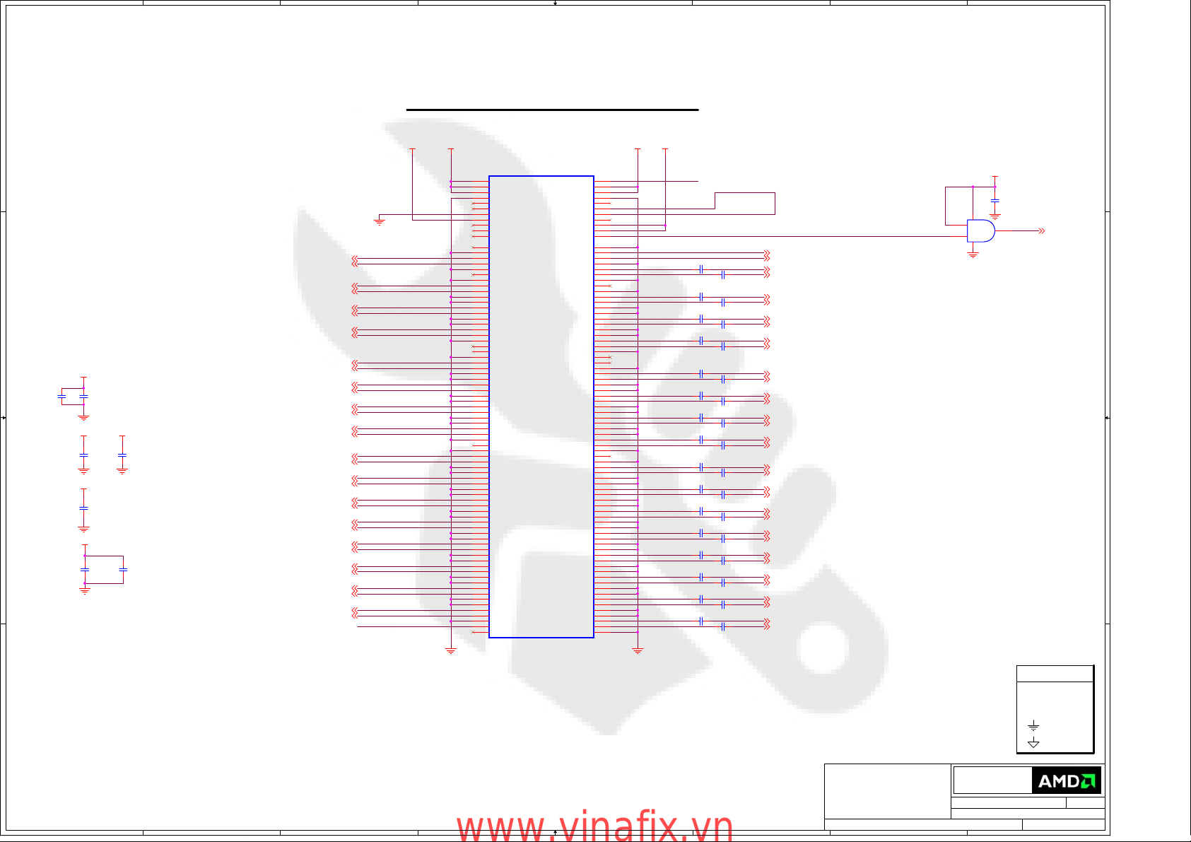
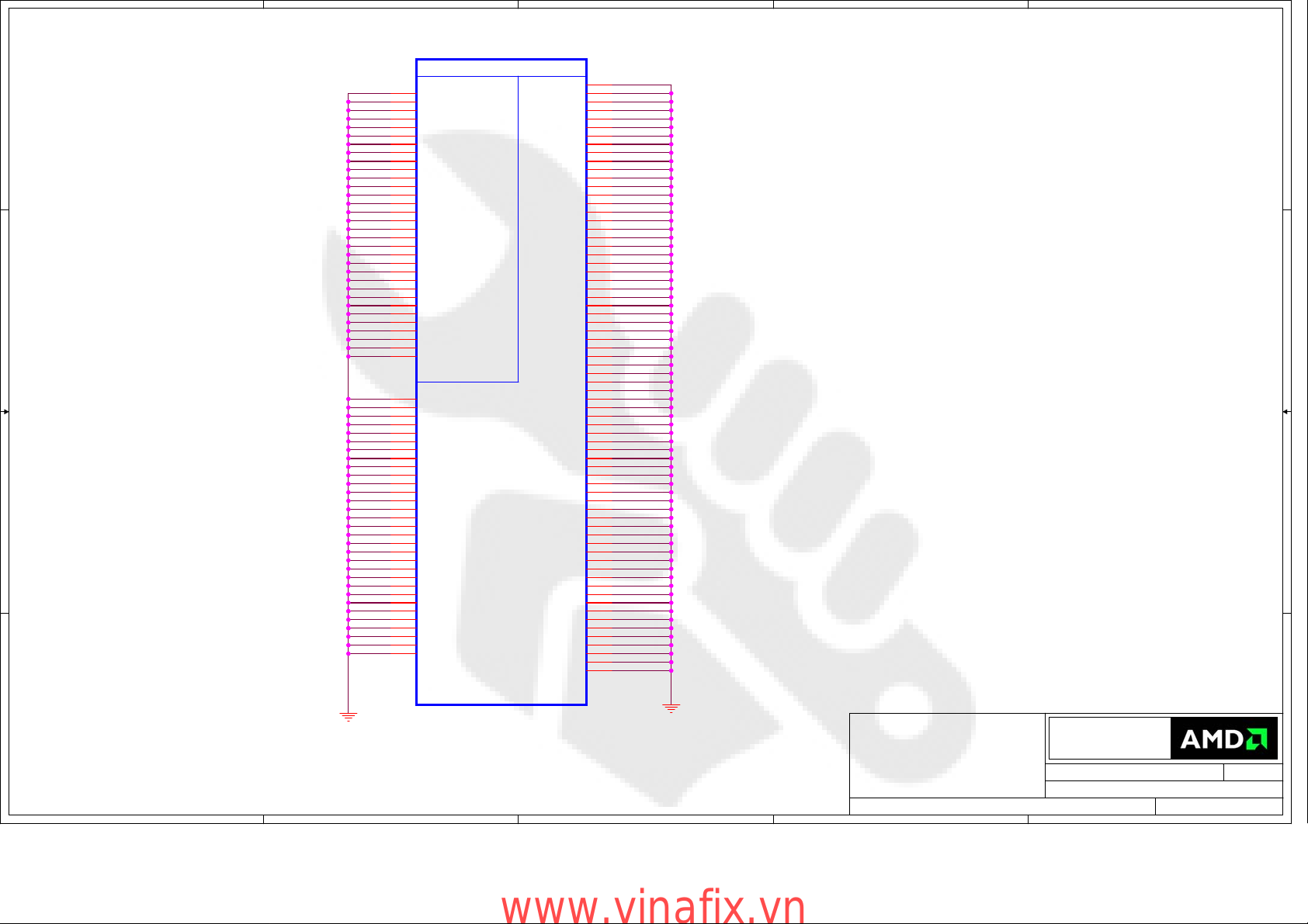
PCI-EXPRESS EDGE CONNECTOR
+12V_BUS+3.3V_BUS +3.3V_BUS+12V_BUS
x16 PCIe
B1
B2
B3
B4
B5
B6
B7
B8
B9
B10
B11
B12
B13
B14
B15
B16
B17
B18
B19
B20
B21
B22
B23
B24
B25
B26
B27
B28
B29
B30
B31
B32
B33
B34
B35
B36
B37
B38
B39
B40
B41
B42
B43
B44
B45
B46
B47
B48
B49
B50
B51
B52
B53
B54
B55
B56
B57
B58
B59
B60
B61
B62
B63
B64
B65
B66
B67
B68
B69
B70
B71
B72
B73
B74
B75
B76
B77
B78
B79
B80
B81
B82
+12V#B1
+12V#B2
+12V#B3
GND#B4
SMCLK
SMDAT
GND#B7
+3.3V#B8
JTAG1
3.3Vaux
WAKE#
RSVD#B12
GND#B13
PETp0
PETn0
GND#B16
PRSNT2#B17
GND#B18
PETp1
PETn1
GND#B21
GND#B22
PETp2
PETn2
GND#B25
GND#B26
PETp3
PETn3
GND#B29
RSVD#B30
PRSNT2#B31
GND#B32
PETp4
PETn4
GND#B35
GND#B36
PETp5
PETn5
GND#B39
GND#B40
PETp6
PETn6
GND#B43
GND#B44
PETp7
PETn7
GND#B47
PRSNT2#B48
GND#B49
PETp8
PETn8
GND#B52
GND#B53
PETp9
PETn9
GND#B56
GND#B57
PETp10
PETn10
GND#B60
GND#B61
PETp11
PETn11
GND#B64
GND#B65
PETp12
PETn12
GND#B68
GND#B69
PETp13
PETn13
GND#B72
GND#B73
PETp14
PETn14
GND#B76
GND#B77
PETp15
PETn15
GND#B80
PRSNT2#B81
RSVD#B82
Mechanical Key
Mechanical Key
x16 PCIe
PRSNT1#A1
+12V#A2
+12V#A3
GND#A4
JTAG2
JTAG3
JTAG4
JTAG5
+3.3V#A9
+3.3V#A10
PERST#
GND#A12
REFCLK+
REFCLKGND#A15
PERp0
PERn0
GND#A18
RSVD#A19
GND#A20
PERp1
PERn1
GND#A23
GND#A24
PERp2
PERn2
GND#A27
GND#A28
PERp3
PERn3
GND#A31
RSVD#A32
RSVD#A33
GND#A34
PERp4
PERn4
GND#A37
GND#A38
PERp5
PERn5
GND#A41
GND#A42
PERp6
PERn6
GND#A45
GND#A46
PERp7
PERn7
GND#A49
RSVD#A50
GND#A51
PERp8
PERn8
GND#A54
GND#A55
PERp9
PERn9
GND#A58
GND#A59
PERp10
PERn10
GND#A62
GND#A63
PERp11
PERn11
GND#A66
GND#A67
PERp12
PERn12
GND#A70
GND#A71
PERp13
PERn13
GND#A74
GND#A75
PERp14
PERn14
GND#A78
GND#A79
PERp15
PERn15
GND#A82
MPCIE1
MPCIE1
A1
A2
A3
A4
A5
A6
A7
A8
A9
A10
A11
A12
A13
A14
A15
A16
A17
A18
A19
A20
A21
A22
A23
A24
A25
A26
A27
A28
A29
A30
A31
A32
A33
A34
A35
A36
A37
A38
A39
A40
A41
A42
A43
A44
A45
A46
A47
A48
A49
A50
A51
A52
A53
A54
A55
A56
A57
A58
A59
A60
A61
A62
A63
A64
A65
A66
A67
A68
A69
A70
A71
A72
A73
A74
A75
A76
A77
A78
A79
A80
A81
A82
PERp0
PERn0
PERp1
PERn1
PERp2
PERn2
PERp3
PERn3
PERp4
PERn4
PERp5
PERn5
PERp6
PERn6
PERp7
PERn7
PERp8
PERn8
PERp9
PERn9
PERp10
PERn10
PERp11
PERn11
PERp12
PERn12
PERp13
PERn13
PERp14
PERn14
PERp15
PERn15
PRESENCE
JTDI
JTDO
C7
100nFC7100nF
C9
100nFC9100nF
C11
C11
100nF
100nF
C13
C13
100nF
100nF
C15
C15
100nF
100nF
C17
C17
100nF
100nF
C19
C19
100nF
100nF
C21
C21
100nF
100nF
C23
C23
100nF
100nF
C25
C25
100nF
100nF
C27
C27
100nF
100nF
C29
C29
100nF
100nF
C31
C31
100nF
100nF
C33
C33
100nF
100nF
C35
C35
100nF
100nF
C37
C37
100nF
100nF
C8
100nFC8100nF
C10
C10
100nF
100nF
C12
C12
100nF
100nF
C14
C14
100nF
100nF
C16
C16
100nF
100nF
C18
C18
100nF
100nF
C20
C20
100nF
100nF
C22
C22
100nF
100nF
C24
C24
100nF
100nF
C26
C26
100nF
100nF
C28
C28
100nF
100nF
C30
C30
100nF
100nF
C32
C32
100nF
100nF
C34
C34
100nF
100nF
C36
C36
100nF
100nF
C38
C38
100nF
100nF
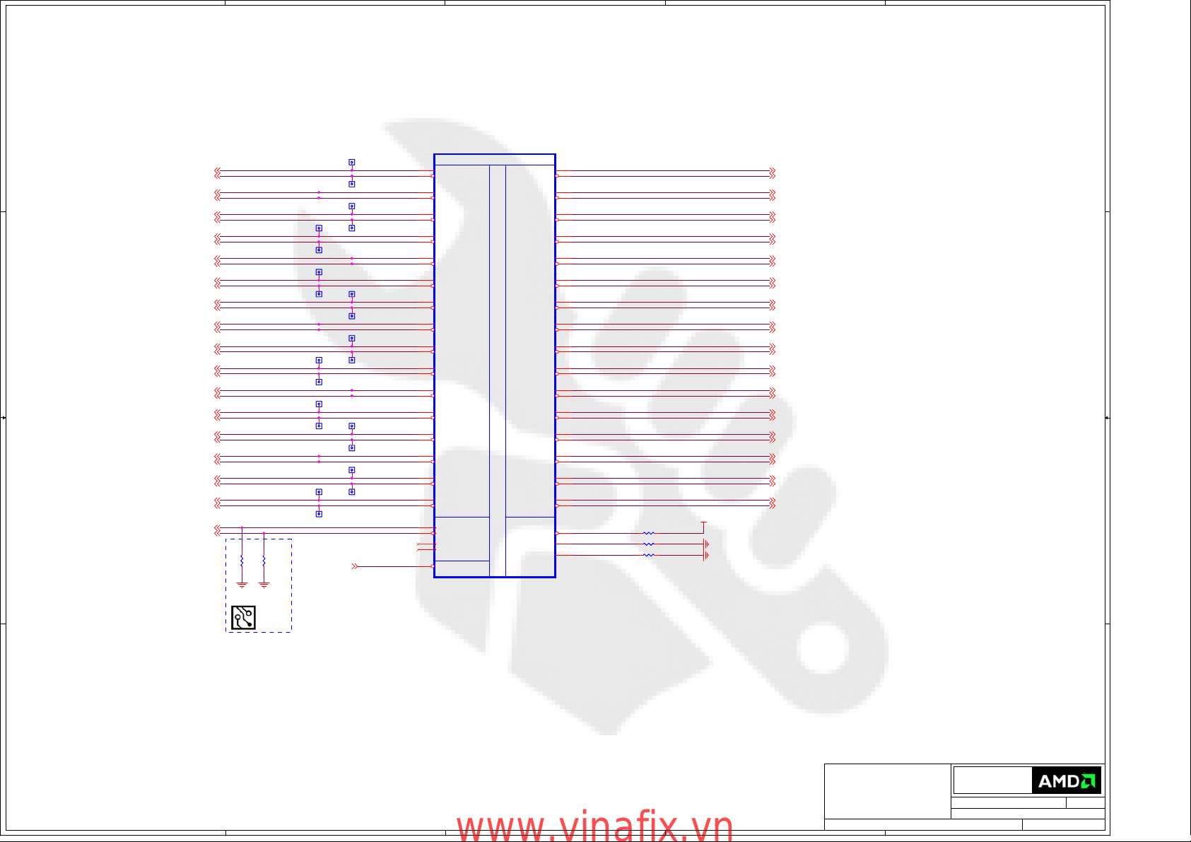
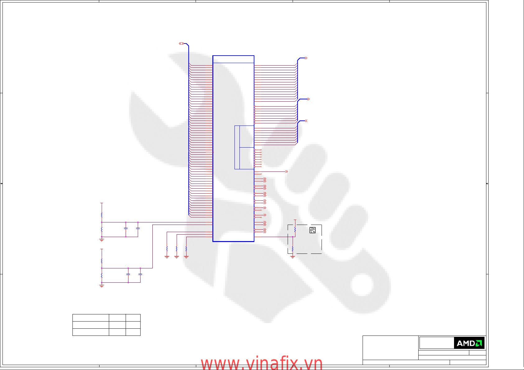
PCIE_REFCLKP {2}
PCIE_REFCLKN {2}PETp0_GFXRp0{2}
GFXTp0_PERp0 {2}
GFXTn0_PERn0 {2}
GFXTp1_PERp1 {2}
GFXTn1_PERn1 {2}
GFXTp2_PERp2 {2}
GFXTn2_PERn2 {2}
GFXTp3_PERp3 {2}
GFXTn3_PERn3 {2}
GFXTp4_PERp4 {2}
GFXTn4_PERn4 {2}
GFXTp5_PERp5 {2}
GFXTn5_PERn5 {2}
GFXTp6_PERp6 {2}
GFXTn6_PERn6 {2}
GFXTp7_PERp7 {2}
GFXTn7_PERn7 {2}
GFXTp8_PERp8 {2}
GFXTn8_PERn8 {2}
GFXTp9_PERp9 {2}
GFXTn9_PERn9 {2}
GFXTp10_PERp10 {2}
GFXTn10_PERn10 {2}
GFXTp11_PERp11 {2}
GFXTn11_PERn11 {2}
GFXTp12_PERp12 {2}
GFXTn12_PERn12 {2}
GFXTp13_PERp13 {2}
GFXTn13_PERn13 {2}
GFXTp14_PERp14 {2}
GFXTn14_PERn14 {2}
GFXTp15_PERp15 {2}
GFXTn15_PERn15 {2}
PERST#
+3.3V
C39
C39
100nF
100nF
53
1
4
2
U5
U5
NC7SZ08P5X_NL
NC7SZ08P5X_NL
PERST#_buf {2}
SYMBOL LEGEND
DNI
DO NOT
INSTALL
#
ACTIVE
LOW
DIGITAL
Doc No.
Doc No.
Doc No.
1
GROUND
ANALOG
GROUND
RevDate:
RevDate:
RevDate:
17
17
17
105-B350xx-00C
105-B350xx-00C
105-B350xx-00C
A A
CONFIDENTIAL & PROPRIETARY TO ADVANCED MICRO DEVICES INC.
CONFIDENTIAL & PROPRIETARY TO ADVANCED MICRO DEVICES INC.
CONFIDENTIAL & PROPRIETARY TO ADVANCED MICRO DEVICES INC.
?2007 Advanced Micro Devices
?2007 Advanced Micro Devices
?2007 Advanced Micro Devices
This AMD Board schematic and design is the exclusive property of AMD,
This AMD Board schematic and design is the exclusive property of AMD,
This AMD Board schematic and design is the exclusive property of AMD,
and is provided only to entities under a non-disclosure agreement
and is provided only to entities under a non-disclosure agreement
and is provided only to entities under a non-disclosure agreement
with AMD for evaluation purposes. Further distribution or disclosure
with AMD for evaluation purposes. Further distribution or disclosure
with AMD for evaluation purposes. Further distribution or disclosure
is strictly prohibited. Use of this schematic and design for any purpose
is strictly prohibited. Use of this schematic and design for any purpose
is strictly prohibited. Use of this schematic and design for any purpose
other than evaluation requires a Board Technology License Agreement
other than evaluation requires a Board Technology License Agreement
other than evaluation requires a Board Technology License Agreement
with AMD. AMD makes no representations or warranties of any kind
with AMD. AMD makes no representations or warranties of any kind
with AMD. AMD makes no representations or warranties of any kind
regarding this schematic and design, including, not limited to,
regarding this schematic and design, including, not limited to,
regarding this schematic and design, including, not limited to,
any implied warranty of merchantibility or fitness for a particular
any implied warranty of merchantibility or fitness for a particular
any implied warranty of merchantibility or fitness for a particular
purpose, and disclaims responsibility forany consequences resulting
purpose, and disclaims responsibility forany consequences resulting
purpose, and disclaims responsibility forany consequences resulting
from use of the information included herein.
from use of the information included herein.
from use of the information included herein.
Title
Title
Title
RH RV620 256/128MB DDR2-BGA84 32/16Mx16 VO dDVI
RH RV620 256/128MB DDR2-BGA84 32/16Mx16 VO dDVI
8
7
6
5
www.vinafix.vn
4
3
RH RV620 256/128MB DDR2-BGA84 32/16Mx16 VO dDVI
2
Advanced Micro Devices Inc.
Advanced Micro Devices Inc.
Advanced Micro Devices Inc.
1 Commerce Valley Drive East
1 Commerce Valley Drive East
1 Commerce Valley Drive East
Markham, Ontario
Markham, Ontario
Markham, Ontario
Wednesday, February 13, 2008
Wednesday, February 13, 2008
Wednesday, February 13, 2008
Sheet
Sheet
Sheet
of
120
of
120
of
120
Page 2
5
D D
4
3
2
1
NOTE: some of the PCIE testpoints will
be available through via on traces.
PETp0_GFXRp0{1}
PETn0_GFXRn0{1}
PETp1_GFXRp1{1}
PETn1_GFXRn1{1}
PETp2_GFXRp2{1}
PETn2_GFXRn2{1}
PETp3_GFXRp3{1}
PETn3_GFXRn3{1}
PETp4_GFXRp4{1}
PETn4_GFXRn4{1}
PETp5_GFXRp5{1}
PETn5_GFXRn5{1}
PETp6_GFXRp6{1}
C C
B B
PETn6_GFXRn6{1}
PETp7_GFXRp7{1}
PETn7_GFXRn7{1}
PETp8_GFXRp8{1}
PETn8_GFXRn8{1}
PETp9_GFXRp9{1}
PETn9_GFXRn9{1}
PETp10_GFXRp10{1}
PETn10_GFXRn10{1}
PETp11_GFXRp11{1}
PETn11_GFXRn11{1}
PETp12_GFXRp12{1}
PETn12_GFXRn12{1}
PETp13_GFXRp13{1}
PETn13_GFXRn13{1}
PETp14_GFXRp14{1}
PETn14_GFXRn14{1}
PETp15_GFXRp15{1}
PETn15_GFXRn15{1}
PCIE_REFCLKP{1}
PCIE_REFCLKN{1}
DNI DNI
R13
R13
51R
51R
402 402
R14
R14
51R
51R
TP7TP7
TP8TP8
TP9TP9
TP10TP10
TP11TP11
TP12TP12
TP13TP13
TP14TP14
TP15TP15
TP16TP16
TP17TP17
TP19TP19
TP18TP18
TP20TP20
TP21TP21
TP23TP23TP22TP22
TP24TP24
TP25TP25
TP26TP26
TP27TP27
TP28TP28
PERST#_buf{1}
AC30
AC31
AC29
AB29
AB31
AB30
AA31
AA30
AD29
AD30
AC28
AC27
AG25
W30
W31
W29
V29
V31
V30
U31
U30
P30
P31
P29
N29
N31
N30
M31
M30
K30
K31
K29
J29
J31
J30
H31
H30
U1A
U1A
PCIE_RX0P
PCIE_RX0N
PCIE_RX1P
PCIE_RX1N
PCIE_RX2P
PCIE_RX2N
PCIE_RX3P
PCIE_RX3N
PCIE_RX4P
PCIE_RX4N
PCIE_RX5P
PCIE_RX5N
PCIE_RX6P
PCIE_RX6N
PCIE_RX7P
PCIE_RX7N
PCIE_RX8P
PCIE_RX8N
PCIE_RX9P
PCIE_RX9N
PCIE_RX10P
PCIE_RX10N
PCIE_RX11P
PCIE_RX11N
PCIE_RX12P
PCIE_RX12N
PCIE_RX13P
PCIE_RX13N
PCIE_RX14P
PCIE_RX14N
PCIE_RX15P
PCIE_RX15N
Clock
Clock
PCIE_REFCLKP
PCIE_REFCLKN
NC_SMBCLK
NC_SMBDATA
PERSTB
RV620 GL A11 RH
RV620 GL A11 RH
PART 1 OF 6
PART 1 OF 6
P
P
C
C
I
I
-
E
E
X
X
P
P
R
R
E
E
S
S
S
S
I
I
N
N
T
T
E
E
R
R
F
F
A
A
C
C
E
E
PCIE_TX0P
PCIE_TX0N
PCIE_TX1P
PCIE_TX1N
PCIE_TX2P
PCIE_TX2N
PCIE_TX3P
PCIE_TX3N
PCIE_TX4P
PCIE_TX4N
PCIE_TX5P
PCIE_TX5N
PCIE_TX6P
PCIE_TX6N
PCIE_TX7P
PCIE_TX7N
PCIE_TX8P
PCIE_TX8N
PCIE_TX9P
PCIE_TX9N
PCIE_TX10P
PCIE_TX10N
PCIE_TX11P
PCIE_TX11N
PCIE_TX12P
PCIE_TX12N
PCIE_TX13P
PCIE_TX13N
PCIE_TX14P
PCIE_TX14N
PCIE_TX15P
PCIE_TX15N
Calibration
Calibration
PCIE_CALRN
PCIE_CALRP
AA28
AA27
AA25
AA24
Y28
Y27
Y25
Y24
V28
V27
V25
V24
T28
T27
T25
T24
P28
P27
P25
P24
M28
M27
M25
M24
L28
L27
L25
L24
J28
J27
G28
G27
+1.1V
PCIE_CALRN
AF25
PCIE_CALRP
AE25
PCIE_CALI
AE23
NC
402
R82.0K R82.0K
402
R91.27K R91.27K
402
R1010K R1010K
GFXTp0_PERp0 {1}
GFXTn0_PERn0 {1}
GFXTp1_PERp1 {1}
GFXTn1_PERn1 {1}
GFXTp2_PERp2 {1}
GFXTn2_PERn2 {1}
GFXTp3_PERp3 {1}
GFXTn3_PERn3 {1}
GFXTp4_PERp4 {1}
GFXTn4_PERn4 {1}
GFXTp5_PERp5 {1}
GFXTn5_PERn5 {1}
GFXTp6_PERp6 {1}
GFXTn6_PERn6 {1}
GFXTp7_PERp7 {1}
GFXTn7_PERn7 {1}
GFXTp8_PERp8 {1}
GFXTn8_PERn8 {1}
GFXTp9_PERp9 {1}
GFXTn9_PERn9 {1}
GFXTp10_PERp10 {1}
GFXTn10_PERn10 {1}
GFXTp11_PERp11 {1}
GFXTn11_PERn11 {1}
GFXTp12_PERp12 {1}
GFXTn12_PERn12 {1}
GFXTp13_PERp13 {1}
GFXTn13_PERn13 {1}
GFXTp14_PERp14 {1}
GFXTn14_PERn14 {1}
GFXTp15_PERp15 {1}
GFXTn15_PERn15 {1}
For Tektronix LA only
Place close
to ASIC
A A
CONFIDENTIAL & PROPRIETARY TO ADVANCED MICRO DEVICES INC.
CONFIDENTIAL & PROPRIETARY TO ADVANCED MICRO DEVICES INC.
CONFIDENTIAL & PROPRIETARY TO ADVANCED MICRO DEVICES INC.
?2007 Advanced Micro Devices
?2007 Advanced Micro Devices
?2007 Advanced Micro Devices
This AMD Board schematic and design is the exclusive property of AMD,
This AMD Board schematic and design is the exclusive property of AMD,
This AMD Board schematic and design is the exclusive property of AMD,
and is provided only to entities under a non-disclosure agreement
and is provided only to entities under a non-disclosure agreement
and is provided only to entities under a non-disclosure agreement
with AMD for evaluation purposes. Further distribution or disclosure
with AMD for evaluation purposes. Further distribution or disclosure
with AMD for evaluation purposes. Further distribution or disclosure
is strictly prohibited. Use of this schematic and design for any purpose
is strictly prohibited. Use of this schematic and design for any purpose
is strictly prohibited. Use of this schematic and design for any purpose
other than evaluation requires a Board Technology License Agreement
other than evaluation requires a Board Technology License Agreement
other than evaluation requires a Board Technology License Agreement
with AMD. AMD makes no representations or warranties of any kind
with AMD. AMD makes no representations or warranties of any kind
with AMD. AMD makes no representations or warranties of any kind
regarding this schematic and design, including, not limited to,
regarding this schematic and design, including, not limited to,
regarding this schematic and design, including, not limited to,
any implied warranty of merchantibility or fitness for a particular
any implied warranty of merchantibility or fitness for a particular
any implied warranty of merchantibility or fitness for a particular
purpose, and disclaims responsibility forany consequences resulting
purpose, and disclaims responsibility forany consequences resulting
purpose, and disclaims responsibility forany consequences resulting
from use of the information included herein.
from use of the information included herein.
from use of the information included herein.
Title
Title
Title
RH RV620 256/128MB DDR2-BGA84 32/16Mx16 VO dDVI
RH RV620 256/128MB DDR2-BGA84 32/16Mx16 VO dDVI
5
4
www.vinafix.vn
3
2
RH RV620 256/128MB DDR2-BGA84 32/16Mx16 VO dDVI
Advanced Micro Devices Inc.
Advanced Micro Devices Inc.
Advanced Micro Devices Inc.
1 Commerce Valley Drive East
1 Commerce Valley Drive East
1 Commerce Valley Drive East
Markham, Ontario
Markham, Ontario
Markham, Ontario
Wednesday, February 13, 2008
Wednesday, February 13, 2008
Wednesday, February 13, 2008
Sheet
Sheet
Sheet
of
220
of
220
of
220
1
Doc No.
Doc No.
Doc No.
RevDate:
RevDate:
RevDate:
17
17
17
105-B350xx-00C
105-B350xx-00C
105-B350xx-00C
Page 3
5
PSYNC{4,13}
VID_6{13}
VID_7{13}
D D
+3.3V
PSYNC
VID_6
VID_7
4
U1B
AE7
AH6
AG6
U1B
PSYNC_NEW
GEN_D_HPD4
GEN_E
MISC/I2C
MISC/I2C
PART 2 OF 6
PART 2 OF 6
PLL Power
PLL Power
DPLL_PVDD
DPLL_PVSS
PCIE_PVDD
AH12
AG12
AH31
+DPLL_PVDD
GND_PVSS
+PCIE_PVDD
1uF_6.3V
1uF_6.3V
C72
C72
10uF_X6S
10uF_X6S
GND_PVSS
C933
C933
C932
C932
10uF_X6S
10uF_X6S
100nF
100nF
3
2
1
+DPLL_PVDD
C70
C70
C71
C71
10nF
C931
C931
100nF
100nF
10nF
NS70NS_VIA NS70NS_VIA
12
+1.8V_D2
B931
B931
BLM15BD121SN1
BLM15BD121SN1
R47
R47
R48
R48
4.7K
4.7K
4.7K
4.7K
C C
GPIO_[13..0]{13}
FLOW_CONTROL_1 - Lower Cable
FLOW_CONTROL_2 - Upper Cable
SWAP_LOCK_1 - Lower Cable
SWAP_LOCK_2 - Upper Cable
GPIO_8
R30 33RR30 33R
GPIO_9
R31 33RR31 33R
GPIO_10
R32 33RR32 33R
GPIO_16 IS OUT ONLY
B B
PWRCNTL_0{13}
GPIO21_BB_EN{13}
GPIO_22{13}
R33 33RR33 33R
MR51KMR5
1K
+1.8V_D2
TP50TP50
R43 221RR43 221R
R44 110RR44 110R
C46 100nFC46 100nF
R_RTCLK
EC82 20PFEC82 20PF
EY82
EY82
27_MHZ
27_MHZ
2 1
EC83 20PFEC83 20PF
Change to 10ppm/10ppm p/n 5028270000G
A A
R84
R84
1.0M
1.0M
Place R_RTCLK close to XTAL so the
main clock line has shortest stub
DVALID
SCL
SDA
GPIO_0
GPIO_1
GPIO_2
GPIO_3
GPIO_4
GPIO_5
GPIO_6
GPIO_7
GPIO8_SO
GPIO9_SI
GPIO10_SCK
GPIO_11
GPIO_12
GPIO_13
PWRCNTL_0
GPIO_18
GPIO21_BB_EN
GPIO22_CS
GENERICA
GENERICB
GENERICC
VREFG
XTALIN
XTALOUT
AD9
DVALID
AA4
SDA
AA5
SCL
AK4
DVPCNTL_MVP_0
AL3
DVPCNTL_MVP_1
V2
DVPCNTL_0
V1
DVPCNTL_1
W3
DVPCNTL_2
W1
DVPCLK
Y1
DVPDATA_0
Y2
DVPDATA_1
Y3
DVPDATA_2
AA2
DVPDATA_3
AA3
DVPDATA_4
AB1
DVPDATA_5
AB2
DVPDATA_6
AB3
DVPDATA_7
AC1
DVPDATA_8
AC3
DVPDATA_9
AD1
DVPDATA_10
AD2
DVPDATA_11
AD3
DVPDATA_12
AF3
DVPDATA_13
AG3
DVPDATA_14
AH3
DVPDATA_15
AG1
DVPDATA_16
AH2
DVPDATA_17
AH1
DVPDATA_18
AJ3
DVPDATA_19
AJ1
DVPDATA_20
AJ2
DVPDATA_21
AK2
DVPDATA_22
AK3
DVPDATA_23
Y4
GPIO_0
V3
GPIO_1
V4
GPIO_2
V5
GPIO_3
U3
GPIO_4
U2
GPIO_5
T4
GPIO_6
T5
GPIO_7_BLON
T7
GPIO_8_ROMSO
T8
GPIO_9_ROMSI
R1
GPIO_10_ROMSCK
R2
GPIO_11
R3
GPIO_12
P1
GPIO_13
P3
GPIO_14_HPD2
N1
GPIO_15_PWRCNTL0
N2
GPIO_16_SSIN
P4
GPIO_17_THERMAL_INT
P7
GPIO_18_HPD3
P8
GPIO_19_CTFB
P5
GPIO_20_PWRCNTL1
V7
GPIO_21_BB_EN
N3
GPIO_22_ROMCSB
Y5
GPIO_23_CLKREQB
M4
GPIO_24_JMODE
M5
GPIO_25_TDI
M7
GPIO_26_TCK
M8
GPIO_27_TMS
L8
GPIO_28_TDO
Y8
GENERICA
Y7
GENERICB
V8
GENERICC
AC11
VREFG
AJ31
XTALIN
AJ30
XTALOUT
RV620 GL A11 RH
RV620 GL A11 RH
External
External
TMDS
TMDS
General
General
Purpose
Purpose
I/O
I/O
XTAL
XTAL
DPLL_VDDC
DAC / CRT
DAC / CRT
DAC2 (TV/CRT2)
DAC2 (TV/CRT2)
V2SYNC
H2SYNC
A2VDDQ
A2VSSQ
DDC1DATA
DDC1CLK
Monitor
Monitor
Interface
Interface
DDC2DATA
DDC2CLK
DDC3DATA_DP3_AUXN
DDC3CLK_DP3_AUXP
TS_FDO
Thermal
Thermal
DMINUS
TESTEN
Test
Test
PLLTEST
DVALID{13}
GPIO_18{13}
PCIE_CLK_REQb
JTAG_MODE
GENERICA{16}
GENERICB{13}
GENERICC{13}
XTALIN
MPVDD
MPVSS
HSYNC
VSYNC
RSET
AVDD
AVSSQ
VDD1DI
VSS1DI
COMP
A2VDD
VDD2DI
VSS2DI
R2SET
HPD1
DPLUS
+MPVDD
A9
C84
C84
C85
C85
C86
C86
C76
C76
100nF
100nF
10nF
GND_MPVSS
B9
+DPLL_VDDC
AE12
AL28
AK28
AL27
AK27
AL26
AK26
AK29
AK30
AJ28
AL29
AH28
AJ27
AJ26
AL17
AK17
AL15
AK15
AL14
AK14
AJ17
AJ15
AJ14
AE16
AF16
AH14
AH16
AG16
AF18
AE18
AG14
AA8
AJ29
AH29
AC5
AC4
AF4
AH4
AE14
AE5
AE4
AH26
AD12
A_R_DAC1 {14}
A_RB_DAC1 {14}
A_G_DAC1 {14}
A_GB_DAC1 {14}
A_B_DAC1 {14}
A_BB_DAC1 {14}
A_HSYNC_DAC1 {13,14}
A_VSYNC_DAC1 {13,14}
RSET
R1030 499RR1030 499R
+AVDD
+VDD1DI
A_VSYNC_DAC2 {13,15}
A_HSYNC_DAC2 {13,15}
+A2VDDQ
TEST_EN
C1020
C1020
10nF
10nF
10V X7R
402 10%
C1023
C1023
10nF
10nF
A_R_DAC2 {15}
A_RB_DAC2 {15}
A_G_DAC2 {15}
A_GB_DAC2 {15}
A_B_DAC2 {15}
A_BB_DAC2 {15}
DAC2_C {16}
DAC2_Y {16}
DAC2_COMP {16}
C2021
C2021
100nF
100nF
C2024
C2024
10nF
10nF
R2SET
HPD1 {14}
CRT1DDCDATA {14}
CRT1DDCCLK {14}
CRT2DDCDATA {15}
CRT2DDCCLK {15}
C1021
C1021
100nF
100nF
10V X5R
402 10%
C1024
C1024
100nF
100nF
C2022
C2022
1uF_6.3V
1uF_6.3V
MR71KMR7
1K
GND_PVSS
C2025
C2025
100nF
100nF
R2030 715RR2030 715R
R
RB
G
GB
B
BB
R2
R2B
G2
G2B
B2
B2B
C
Y
10nF
C60
C60
C61
C61
10nF
10nF
100nF
100nF
C1022
C1022
NS1020NS_VIANS1020NS_VIA
1uF_6.3V
1uF_6.3V
6.3V X5R
402 10%
NS1021NS_VIANS1021NS_VIA
C1025
C1025
1uF_6.3V
1uF_6.3V
GND_VSS1DI
+A2VDD +3.3V
B2030 120R_300mAB2030 120R_300mA
C2031
C2031
C2032
C2032
100nF
100nF
1uF_6.3V
1uF_6.3V
+VDD2DI
C2026
C2026
1uF_6.3V
1uF_6.3V
+3.3V
R41
R41
R40
R40
4.7K
4.7K
4.7K
4.7K
402 402
1uF_6.3V
1uF_6.3V
1uF_6.3V
1uF_6.3V
GND_MPVSS
C63
C63
C62
C62
10uF_X6S
10uF_X6S
1uF_6.3V
1uF_6.3V
GND_AVSSQ
12
GND_AVSSQ
12
Possible alternate 5150005600G
NS2020NS_VIANS2020NS_VIA
12
GND_A2VSSQ
NS2021NS_VIANS2021NS_VIA
12
GND_VSS2DI
GND_A2VSSQ
I2C DEVICE ADDRESS' ON DDC3
DEVICE
ADDRESS
LM63
x100 1100
DDC3DATA
DDC3CLK
XTALOUT
+VDDC
B6760R B6760R
NS64NS_VIA NS64NS_VIA
12
+1.1V
B60
B60
BLM15BD121SN1
BLM15BD121SN1
GPIO_22
GPIO_8
+3.3V
ROM_WP
+3.3V
R46
R46
10K
10K
U2
U2
1
CE#
2
SO
3
WP#
GND4SI
PM25LV512A-100SCE
PM25LV512A-100SCE
NEW CHINGIS SERIAL FLASH
8
VCC
7
HOLD#
GPIO_10
6
SCK
GPIO_9
5
BIOS1
BIOS1
BIOS
BIOS
113-XXXXXX-XXX
113-XXXXXX-XXX
VIDEO BIOS
FIRMWARE
+3.3V
C47
C47
100nF
100nF
CONFIDENTIAL & PROPRIETARY TO ADVANCED MICRO DEVICES INC.
CONFIDENTIAL & PROPRIETARY TO ADVANCED MICRO DEVICES INC.
CONFIDENTIAL & PROPRIETARY TO ADVANCED MICRO DEVICES INC.
?2007 Advanced Micro Devices
?2007 Advanced Micro Devices
?2007 Advanced Micro Devices
This AMD Board schematic and design is the exclusive property of AMD,
This AMD Board schematic and design is the exclusive property of AMD,
This AMD Board schematic and design is the exclusive property of AMD,
and is provided only to entities under a non-disclosure agreement
and is provided only to entities under a non-disclosure agreement
and is provided only to entities under a non-disclosure agreement
with AMD for evaluation purposes. Further distribution or disclosure
with AMD for evaluation purposes. Further distribution or disclosure
with AMD for evaluation purposes. Further distribution or disclosure
is strictly prohibited. Use of this schematic and design for any purpose
is strictly prohibited. Use of this schematic and design for any purpose
is strictly prohibited. Use of this schematic and design for any purpose
other than evaluation requires a Board Technology License Agreement
other than evaluation requires a Board Technology License Agreement
other than evaluation requires a Board Technology License Agreement
with AMD. AMD makes no representations or warranties of any kind
with AMD. AMD makes no representations or warranties of any kind
with AMD. AMD makes no representations or warranties of any kind
regarding this schematic and design, including, not limited to,
regarding this schematic and design, including, not limited to,
regarding this schematic and design, including, not limited to,
any implied warranty of merchantibility or fitness for a particular
any implied warranty of merchantibility or fitness for a particular
any implied warranty of merchantibility or fitness for a particular
purpose, and disclaims responsibility forany consequences resulting
purpose, and disclaims responsibility forany consequences resulting
purpose, and disclaims responsibility forany consequences resulting
from use of the information included herein.
from use of the information included herein.
from use of the information included herein.
Title
Title
Title
RH RV620 256/128MB DDR2-BGA84 32/16Mx16 VO dDVI
RH RV620 256/128MB DDR2-BGA84 32/16Mx16 VO dDVI
5
4
3
2
RH RV620 256/128MB DDR2-BGA84 32/16Mx16 VO dDVI
Advanced Micro Devices Inc.
Advanced Micro Devices Inc.
Advanced Micro Devices Inc.
1 Commerce Valley Drive East
1 Commerce Valley Drive East
1 Commerce Valley Drive East
Markham, Ontario
Markham, Ontario
Markham, Ontario
Wednesday, February 13, 2008
Wednesday, February 13, 2008
Wednesday, February 13, 2008
Sheet
Sheet
Sheet
of
320
of
320
of
320
1
Doc No.
Doc No.
Doc No.
RevDate:
RevDate:
RevDate:
17
17
17
105-B350xx-00C
105-B350xx-00C
105-B350xx-00C
www.vinafix.vn
Page 4
5
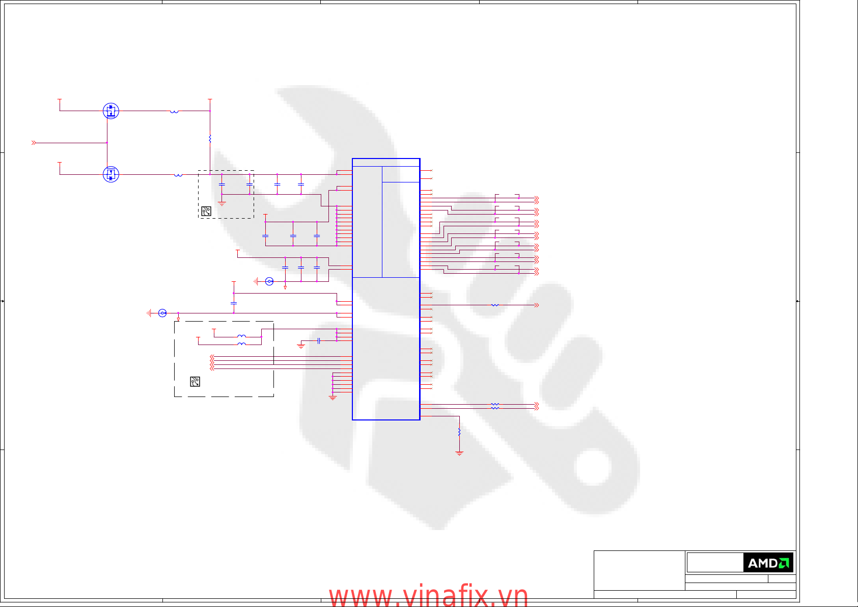
D D
+1.8V_D2
1
Q100
Q100
SI2304DS
SI2304DS
LTVDD18_IN
32
B100
B100
BLM15BD121SN1
BLM15BD121SN1
+LTVDD18
LVT_EN{9}
SI2304DS
+3.3V_BUS
C C
B B
SI2304DS
1
Q101
Q101
LTVDD33_IN
32
GND_TPVSS
PLEASE SEE p.13 FOR STRAP DETAILS
1 2
B101
B101
BLM15BD121SN1
BLM15BD121SN1
NS110NS_VIA NS110NS_VIA
C119
C119
4.7uF_6.3V
4.7uF_6.3V
+1.8V_D2
+1.1V
DPAVSS-VID5{13}
DPAVSS-VID4{13}
DPVSS-VID0{13}
DPAVSS-VID3{13}
OVERLAP
4
R1100RR110
0R
C118
C118
10uF_X6S
10uF_X6S
OVERLAP C119 & C118
+1.8V_D2
+TPVDD
C110
C110
10nF
10nF
BLM15BD121SN1
BLM15BD121SN1
BLM15BD121SN1
BLM15BD121SN1
INSTALL B888 FOR RV610
INSTALL B881 FOR RV620
RV620: INSTALL R110, DNI B101, Q101.
RV610: DNI R110
RV620 DECOUPLING RECOMMENDATIONS FOR T2XVDDR/C WILL
BE AVAILABLE AFTER BU. C118 AND C103 WILL NOT BOTH BE
INSTALLED.
C106
C106
1uF_6.3V
1uF_6.3V
C105
C105
100nF
100nF
LVDDR
AG20
AH20
+LTVDD18
AK18
AK23
+TPVDD
AK25
AG18
AH18
AE11
AK13
C11410nF C11410nF
C103
C103
10uF_X6S
10uF_X6S
B888
B888
B881
B881
10uF_X6S
10uF_X6S
1 2
1uF_6.3V
1uF_6.3V
C102
C102
NS100NS_VIA NS100NS_VIA
C108
C108
C101
C101
100nF
100nF
GND_T2PVSS
C109
C109
100nF
100nF
C100
C100
1uF_6.3V
1uF_6.3V
GND_TPVSS
DPAB_VDDR
DPAVSS-VID5
DPAVSS-VID4
DPVSS-VID0
DPAVSS-VID3
AH11
AK12
U1F
U1F
AF20
T2XVDDR_1
T2XVDDR_2
AJ18
T2XVDDC_1
T2XVDDC_2
AF23
T2XVSSR_1
AF21
T2XVSSR_2
AL18
T2XVSSR_3
AJ22
T2XVSSR_4
AJ25
T2XVSSR_5
T2XVSSR_6
T2XVSSR_7
T2XVSSR_8
AJ21
T2XVSSR_9
AL23
T2XVSSR_10
AL25
T2XVSSR_11
T2PVDD
T2PVSS
AL7
DPA_PVDD
DPB_PVDD
AK7
DPA_PVSS
AF11
DPB_PVSS
AJ12
DPA_VDDR_1
AJ13
DPA_VDDR_2
DPB_VDDR_2
AL13
DPB_VDDR_1
AF7
DPA_VSSR_1
AG7
DPA_VSSR_2
AH7
DPA_VSSR_3
AJ7
DPA_VSSR_4
AJ8
DPA_VSSR_5
DPB_VSSR_1
AL12
DPB_VSSR_2
AH9
DPB_VSSR_3
AJ11
DPB_VSSR_4
DPB_VSSR_5
RV620 GL A11 RH
RV620 GL A11 RH
PART 6 OF 6
PART 6 OF 6
Control
Control
LVTM channel
LVTM channel
Integrated TMDP
Integrated TMDP
DDC4CLK_DP4_AUXP
DDC4DATA_DP4_AUXN
3
RSVD_7
RSVD
RSVD_1
RSVD_2
T2X4P
T2X4M
T2X5P
T2X5M
RSVD_4
RSVD_3
RSVD_6
RSVD_5
T2XCP
T2XCM
T2X0P
T2X0M
T2X1P
T2X1M
T2X2P
T2X2M
T2X3P
T2X3M
TXCM_DPA0P
TXCP_DPA0N
TX0M_DPA1P
TX0P_DPA1N
TX1M_DPA2P
TX1P_DPA2N
TX2M_DPA3P
TX2P_DPA3N
TXCM_DPB0P
TXCP_DPB0N
TX0M_DPB1P
TX0P_DPB1N
TX1M_DPB2P
TX1P_DPB2N
TX2M_DPB3P
TX2P_DPB3N
DP_CALR
AA7
AC6
AD21
AE21
AJ24
AJ23
AK24
AL24
AG21
AH21
AG23
AH23
AL19
AK19
AJ20
AJ19
AK20
AL20
AK21
AL21
AK22
AL22
AJ4
AJ5
AL5
AK5
AL6
AK6
AK8
AL8
AK9
AL9
AJ9
AJ10
AL10
AK10
AL11
AK11
AG9
AF9
AG11
DP_CALR
TjXCP
RV610_PSYNC
DPX-VID1
DPX-VID2
TjX4P
TjX4M
TjX5P
TjX5M
TjXCM
TjX0P
TjX0M
TjX1P
TjX1M
TjX2P
TjX2M
TjX3P
TjX3M
R150 0RR150 0R
RV610 - INSTALL R150-R152
RV620 - DO NOT INSTALL R150-R152
R151 0RR151 0R
R152 0RR152 0R
R153
R153
150R
150R
2
TjX4P {14}
TjX4M {14}
TjX5P {14}
TjX5M {14}
TjXCP {14}
TjXCM {14}
TjX0P {14}
TjX0M {14}
TjX1P {14}
TjX1M {14}
TjX2P {14}
TjX2M {14}
TjX3P {14}
TjX3M {14}
PSYNC {3,13}
VID_1 {13}
VID_2 {13}
1
A A
CONFIDENTIAL & PROPRIETARY TO ADVANCED MICRO DEVICES INC.
CONFIDENTIAL & PROPRIETARY TO ADVANCED MICRO DEVICES INC.
CONFIDENTIAL & PROPRIETARY TO ADVANCED MICRO DEVICES INC.
?2007 Advanced Micro Devices
?2007 Advanced Micro Devices
?2007 Advanced Micro Devices
This AMD Board schematic and design is the exclusive property of AMD,
This AMD Board schematic and design is the exclusive property of AMD,
This AMD Board schematic and design is the exclusive property of AMD,
and is provided only to entities under a non-disclosure agreement
and is provided only to entities under a non-disclosure agreement
and is provided only to entities under a non-disclosure agreement
with AMD for evaluation purposes. Further distribution or disclosure
with AMD for evaluation purposes. Further distribution or disclosure
with AMD for evaluation purposes. Further distribution or disclosure
is strictly prohibited. Use of this schematic and design for any purpose
is strictly prohibited. Use of this schematic and design for any purpose
is strictly prohibited. Use of this schematic and design for any purpose
other than evaluation requires a Board Technology License Agreement
other than evaluation requires a Board Technology License Agreement
other than evaluation requires a Board Technology License Agreement
with AMD. AMD makes no representations or warranties of any kind
with AMD. AMD makes no representations or warranties of any kind
with AMD. AMD makes no representations or warranties of any kind
regarding this schematic and design, including, not limited to,
regarding this schematic and design, including, not limited to,
regarding this schematic and design, including, not limited to,
any implied warranty of merchantibility or fitness for a particular
any implied warranty of merchantibility or fitness for a particular
any implied warranty of merchantibility or fitness for a particular
purpose, and disclaims responsibility forany consequences resulting
purpose, and disclaims responsibility forany consequences resulting
purpose, and disclaims responsibility forany consequences resulting
from use of the information included herein.
from use of the information included herein.
from use of the information included herein.
Title
Title
Title
RH RV620 256/128MB DDR2-BGA84 32/16Mx16 VO dDVI
RH RV620 256/128MB DDR2-BGA84 32/16Mx16 VO dDVI
5
4
www.vinafix.vn
3
2
RH RV620 256/128MB DDR2-BGA84 32/16Mx16 VO dDVI
Advanced Micro Devices Inc.
Advanced Micro Devices Inc.
Advanced Micro Devices Inc.
1 Commerce Valley Drive East
1 Commerce Valley Drive East
1 Commerce Valley Drive East
Markham, Ontario
Markham, Ontario
Markham, Ontario
Wednesday, February 13, 2008
Wednesday, February 13, 2008
Wednesday, February 13, 2008
Sheet
Sheet
Sheet
of
420
of
420
of
420
1
Doc No.
Doc No.
Doc No.
RevDate:
RevDate:
RevDate:
17
17
17
105-B350xx-00C
105-B350xx-00C
105-B350xx-00C
Page 5
5
D D
C C
B B
A A
5
4
U1E
U1E
AA26
PCIE_VSS_1
AA29
PCIE_VSS_2
AC26
PCIE_VSS_3
AD31
PCIE_VSS_4
AE29
PCIE_VSS_5
AE30
PCIE_VSS_6
AE31
PCIE_VSS_7
F28
PCIE_VSS_8
G26
PCIE_VSS_9
G29
PCIE_VSS_10
G30
PCIE_VSS_11
G31
PCIE_VSS_12
H29
PCIE_VSS_13
J25
PCIE_VSS_14
J26
PCIE_VSS_15
L26
PCIE_VSS_16
L29
PCIE_VSS_17
L30
PCIE_VSS_18
L31
PCIE_VSS_19
M26
PCIE_VSS_20
M29
PCIE_VSS_21
P26
PCIE_VSS_22
R29
PCIE_VSS_23
R30
PCIE_VSS_24
R31
PCIE_VSS_25
T26
PCIE_VSS_26
U29
PCIE_VSS_27
V26
PCIE_VSS_28
Y26
PCIE_VSS_29
Y29
PCIE_VSS_30
Y30
PCIE_VSS_31
Y31
PCIE_VSS_32
A13
VSS_1
A2
VSS_2
C18
VSS_3
A24
VSS_4
A30
VSS_5
AA1
VSS_6
AA11
VSS_7
AA14
VSS_8
AA17
VSS_9
AA20
VSS_10
AA6
VSS_11
AC2
VSS_12
AC7
VSS_13
AE3
VSS_15
AL4
VSS_16
AD14
VSS_17
AF12
VSS_18
AF14
VSS_19
AD16
VSS_20
AD18
VSS_21
AE6
VSS_22
AG2
VSS_23
AE9
VSS_24
AH25
VSS_25
AK1
VSS_26
AK31
VSS_27
AJ6
VSS_28
AL2
VSS_29
AL30
VSS_30
B1
VSS_31
C13
VSS_32
CORE GND
CORE GND
RV620 GL A11 RH
RV620 GL A11 RH
4
Part 5 of 6
Part 5 of 6
PCI-Express GND
PCI-Express GND
VSS_33
VSS_34
VSS_35
VSS_36
VSS_37
VSS_38
VSS_39
VSS_40
VSS_41
VSS_42
VSS_43
VSS_44
VSS_45
VSS_46
VSS_47
VSS_48
VSS_49
VSS_50
VSS_51
VSS_52
VSS_53
VSS_54
VSS_55
VSS_56
VSS_57
VSS_58
VSS_59
VSS_60
VSS_61
VSS_62
VSS_63
VSS_64
VSS_65
VSS_66
VSS_67
VSS_68
VSS_69
VSS_70
VSS_71
VSS_72
VSS_73
VSS_74
VSS_75
VSS_76
VSS_77
VSS_78
VSS_79
VSS_80
VSS_81
VSS_82
VSS_83
VSS_84
VSS_85
VSS_86
VSS_87
VSS_88
VSS_89
VSS_90
VSS_91
VSS_92
VSS_93
VSS_94
VSS_95
VSS_96
VSS_97
VSS_98
VSS_99
VSS_100
VSS_101
VSS_102
B25
J8
B5
D11
C17
C22
C27
D29
C3
C6
D3
D28
F29
D4
F11
F12
F14
F16
F18
F20
F21
F23
F25
F7
F9
G3
G6
H23
J3
J4
J6
K1
L12
L15
L18
L21
L6
M11
M14
M17
M20
M6
P12
P15
P18
P21
P6
AC21
R14
R17
R20
T6
U1
U12
U15
U18
U21
AE20
V14
V17
V20
P2
V6
W2
Y12
Y15
Y18
Y21
Y6
M9
3
CONFIDENTIAL & PROPRIETARY TO ADVANCED MICRO DEVICES INC.
CONFIDENTIAL & PROPRIETARY TO ADVANCED MICRO DEVICES INC.
CONFIDENTIAL & PROPRIETARY TO ADVANCED MICRO DEVICES INC.
?2007 Advanced Micro Devices
?2007 Advanced Micro Devices
?2007 Advanced Micro Devices
This AMD Board schematic and design is the exclusive property of AMD,
This AMD Board schematic and design is the exclusive property of AMD,
This AMD Board schematic and design is the exclusive property of AMD,
and is provided only to entities under a non-disclosure agreement
and is provided only to entities under a non-disclosure agreement
and is provided only to entities under a non-disclosure agreement
with AMD for evaluation purposes. Further distribution or disclosure
with AMD for evaluation purposes. Further distribution or disclosure
with AMD for evaluation purposes. Further distribution or disclosure
is strictly prohibited. Use of this schematic and design for any purpose
is strictly prohibited. Use of this schematic and design for any purpose
is strictly prohibited. Use of this schematic and design for any purpose
other than evaluation requires a Board Technology License Agreement
other than evaluation requires a Board Technology License Agreement
other than evaluation requires a Board Technology License Agreement
with AMD. AMD makes no representations or warranties of any kind
with AMD. AMD makes no representations or warranties of any kind
with AMD. AMD makes no representations or warranties of any kind
regarding this schematic and design, including, not limited to,
regarding this schematic and design, including, not limited to,
regarding this schematic and design, including, not limited to,
any implied warranty of merchantibility or fitness for a particular
any implied warranty of merchantibility or fitness for a particular
any implied warranty of merchantibility or fitness for a particular
purpose, and disclaims responsibility forany consequences resulting
purpose, and disclaims responsibility forany consequences resulting
purpose, and disclaims responsibility forany consequences resulting
from use of the information included herein.
from use of the information included herein.
from use of the information included herein.
Title
Title
Title
3
2
Advanced Micro Devices Inc.
Advanced Micro Devices Inc.
Advanced Micro Devices Inc.
1 Commerce Valley Drive East
1 Commerce Valley Drive East
1 Commerce Valley Drive East
Markham, Ontario
Markham, Ontario
Markham, Ontario
Wednesday, February 13, 2008
Wednesday, February 13, 2008
Wednesday, February 13, 2008
Sheet
Sheet
Sheet
RH RV620 256/128MB DDR2-BGA84 32/16Mx16 VO dDVI
RH RV620 256/128MB DDR2-BGA84 32/16Mx16 VO dDVI
RH RV620 256/128MB DDR2-BGA84 32/16Mx16 VO dDVI
2
of
520
of
520
of
520
1
Doc No.
Doc No.
Doc No.
105-B350xx-00C
105-B350xx-00C
105-B350xx-00C
1
RevDate:
RevDate:
RevDate:
17
17
17
www.vinafix.vn
Page 6
5
4
3
2
1
D D
C C
PLACE MVREF DIVIDERS
AND CAPS CLOSE TO ASIC
+MVDD
R291
R291
100R
100R
1%
C296
R292
+MVDD
R292
100R
100R
1%
R293
R293
100R
100R
1%
R294
R294
100R
100R
1%
B B
C295
C295
100nF
100nF
C297
C297
100nF
100nF
C296
10nF
10nF
C298
C298
10nF
10nF
M_MDA[63..0]{8}
U1C
MVREFD_0
MVREFS_0
R296
R296
4.7K
4.7K
U1C
Part 3 of 6
M_MDA0
E29
M_MDA1
E30
M_MDA2
E31
M_MDA3
D31
M_MDA4
C29
M_MDA5
B29
M_MDA6
B30
M_MDA7
A29
M_MDA8
E26
M_MDA9
D26
M_MDA10
E25
M_MDA11
D25
M_MDA12
G23
M_MDA13
G21
M_MDA14
E21
M_MDA15
D21
M_MDA16
C28
M_MDA17
B28
M_MDA18
B27
M_MDA19
A27
M_MDA20
C25
M_MDA21
A25
M_MDA22
C24
M_MDA23
B24
M_MDA24
C23
M_MDA25
B23
M_MDA26
A23
M_MDA27
B22
M_MDA28
C20
M_MDA29
B20
M_MDA30
A20
M_MDA31
C19
M_MDA32
M_MDA33
M_MDA34
M_MDA35
M_MDA36
M_MDA37
M_MDA38
M_MDA39
M_MDA40
G9
M_MDA41
M_MDA42
M_MDA43
G7
M_MDA44
G5
M_MDA45
M_MDA46
G4
M_MDA47
M_MDA48
M_MDA49
M_MDA50
M_MDA51
M_MDA52
M_MDA53
M_MDA54
M_MDA55
M_MDA56
G2
M_MDA57
G1
M_MDA58
M_MDA59
M_MDA60
M_MDA61
M_MDA62
M_MDA63
F30
F31
TEST_MCLK
TEST_YCLK
MEMTEST DRAM_RST
R297
R297
R298
R298
4.7K
4.7K
243R
243R
DQ_0
DQ_1
DQ_2
DQ_3
DQ_4
DQ_5
DQ_6
DQ_7
DQ_8
DQ_9
DQ_10
DQ_11
DQ_12
DQ_13
DQ_14
DQ_15
DQ_16
DQ_17
DQ_18
DQ_19
DQ_20
DQ_21
DQ_22
DQ_23
DQ_24
DQ_25
DQ_26
DQ_27
DQ_28
DQ_29
DQ_30
DQ_31
C8
DQ_32
C7
DQ_33
B7
DQ_34
A7
DQ_35
A5
DQ_36
C4
DQ_37
B4
DQ_38
A3
DQ_39
DQ_40
E9
DQ_41
D9
DQ_42
DQ_43
DQ_44
F5
DQ_45
DQ_46
F4
DQ_47
B3
DQ_48
B2
DQ_49
C2
DQ_50
C1
DQ_51
E3
DQ_52
F3
DQ_53
F2
DQ_54
F1
DQ_55
DQ_56
DQ_57
H3
DQ_58
H2
DQ_59
K2
DQ_60
L3
DQ_61
L2
DQ_62
L1
DQ_63
MVREFD
MVREFS
L5
TEST_MCLK
L7
TEST_YCLK
J7
MEMTEST
RV620 GL A11 RH
RV620 GL A11 RH
Part 3 of 6
MEMORY
MEMORY
INTERFACE
INTERFACE
write strobe read strobe
write strobe read strobe
MA_0
MA_1
MA_2
MA_3
MA_4
MA_5
MA_6
MA_7
MA_8
MA_9
MA_10
MA_11
MA_BA0
MA_BA1
MA_A12
MA_BA2
DQMb_0
DQMb_1
DQMb_2
DQMb_3
DQMb_4
DQMb_5
DQMb_6
DQMb_7
QS_0
QS_1
QS_2
QS_3
QS_4
QS_5
QS_6
QS_7
QS_0B
QS_1B
QS_2B
QS_3B
QS_4B
QS_5B
QS_6B
QS_7B
ODT0
ODT1
CLK0
CLK1
CLK0b
CLK1b
RAS0b
RAS1b
CAS0b
CAS1b
CS0b_0
CS0b_1
CS1b_0
CS1b_1
CKE0
CKE1
WE0b
WE1b
DRAM_RST
M_MAA0
B14
M_MAA1
A14
M_MAA2
B13
M_MAA3
E14
M_MAA4
B17
M_MAA5
A17
M_MAA6
C15
M_MAA7
G16
M_MAA8
E16
M_MAA9
C14
M_MAA10
A12
M_MAA11
B12
M_MAA14
C12
M_MAA15
D14
M_MAA12
B15
M_MAA13
G14
M_DQMA#0
D30
M_DQMA#1
G25
M_DQMA#2
C26
M_DQMA#3
C21
M_DQMA#4
C5
M_DQMA#5
D6
M_DQMA#6
D2
M_DQMA#7
K3
M_QSA0
C30
M_QSA1
D23
M_QSA2
B26
M_QSA3
B21
M_QSA4
B6
M_QSA5
E7
M_QSA6
E2
M_QSA7
J2
C31
E23
A26
A21
A6
D7
E1
J1
E20
C11
A18
CLKA0 {8}
A11
CLKA1 {8}
B18
CLKA#0 {8}
B11
CLKA#1 {8}
G20
RASA#0 {8}
D12
RASA#1 {8}
D20
CASA#0 {8}
E12
CASA#1 {8}
E18
CSA#0_0 {8}
G18
G11
CSA#1_0 {8}
E11
D18
CKEA0 {8}
G12
CKEA1 {8}
D16
WEA#0 {8}
C10
WEA#1 {8}
J5
ODT {8}
+MVDD
DNI
MR295
MR295
4.7K
4.7K
R295
R295
2.0K
2.0K
M_MAA[15..0] {8}
M_DQMA#[7..0] {8}
M_QSA[7..0] {8}
Overlap
A A
5
DIVIDER RESISTORS DDR2 GDDR3
MVREF TO 1.8V
MVREF TO GND
40.2R100R
100R100R
CONFIDENTIAL & PROPRIETARY TO ADVANCED MICRO DEVICES INC.
CONFIDENTIAL & PROPRIETARY TO ADVANCED MICRO DEVICES INC.
CONFIDENTIAL & PROPRIETARY TO ADVANCED MICRO DEVICES INC.
?2007 Advanced Micro Devices
?2007 Advanced Micro Devices
?2007 Advanced Micro Devices
This AMD Board schematic and design is the exclusive property of AMD,
This AMD Board schematic and design is the exclusive property of AMD,
This AMD Board schematic and design is the exclusive property of AMD,
and is provided only to entities under a non-disclosure agreement
and is provided only to entities under a non-disclosure agreement
and is provided only to entities under a non-disclosure agreement
with AMD for evaluation purposes. Further distribution or disclosure
with AMD for evaluation purposes. Further distribution or disclosure
with AMD for evaluation purposes. Further distribution or disclosure
is strictly prohibited. Use of this schematic and design for any purpose
is strictly prohibited. Use of this schematic and design for any purpose
is strictly prohibited. Use of this schematic and design for any purpose
other than evaluation requires a Board Technology License Agreement
other than evaluation requires a Board Technology License Agreement
other than evaluation requires a Board Technology License Agreement
with AMD. AMD makes no representations or warranties of any kind
with AMD. AMD makes no representations or warranties of any kind
with AMD. AMD makes no representations or warranties of any kind
regarding this schematic and design, including, not limited to,
regarding this schematic and design, including, not limited to,
regarding this schematic and design, including, not limited to,
any implied warranty of merchantibility or fitness for a particular
any implied warranty of merchantibility or fitness for a particular
any implied warranty of merchantibility or fitness for a particular
purpose, and disclaims responsibility forany consequences resulting
purpose, and disclaims responsibility forany consequences resulting
purpose, and disclaims responsibility forany consequences resulting
from use of the information included herein.
from use of the information included herein.
from use of the information included herein.
Title
Title
Title
RH RV620 256/128MB DDR2-BGA84 32/16Mx16 VO dDVI
RH RV620 256/128MB DDR2-BGA84 32/16Mx16 VO dDVI
4
www.vinafix.vn
3
2
RH RV620 256/128MB DDR2-BGA84 32/16Mx16 VO dDVI
Advanced Micro Devices Inc.
Advanced Micro Devices Inc.
Advanced Micro Devices Inc.
1 Commerce Valley Drive East
1 Commerce Valley Drive East
1 Commerce Valley Drive East
Markham, Ontario
Markham, Ontario
Markham, Ontario
Wednesday, February 13, 2008
Wednesday, February 13, 2008
Wednesday, February 13, 2008
Sheet
Sheet
Sheet
of
620
of
620
of
620
1
Doc No.
Doc No.
Doc No.
RevDate:
RevDate:
RevDate:
17
17
17
105-B350xx-00C
105-B350xx-00C
105-B350xx-00C
Page 7

5
D D
C134
C134
10uF_X6S
10uF_X6S
Recommended caps:
(see BOM for qualified values/vendors)
10uF , X6S, 10%, 0805, 6.3V, 1.4MM MAX THICK
1uF, X6S, 10%, 0402, 6.3V
100nF, X7R, 10%, 0402
10nF , X7R, 10%, 0402
C C
B B
C135
C135
10uF_X6S
10uF_X6S
+MVDD
C136
C136
10uF_X6S
10uF_X6S
C125
C125
C124
C124
10nF
10nF
10nF
10nF
C137
C137
C138
C138
10uF_X6S
10uF_X6S
1uF_6.3V
1uF_6.3V
+MVDD
B120 BLM15BD121SN1B120 BLM15BD121SN1
B121 BLM15BD121SN1B121 BLM15BD121SN1
NS121 NS_VIANS121 NS_VIA
C126
C126
10nF
10nF
C139
C139
1uF_6.3V
1uF_6.3V
C120
C120
1uF_6.3V
1uF_6.3V
12
GND_VSSRH0
+1.8V_D2
C127
C127
10nF
10nF
C140
C140
1uF_6.3V
1uF_6.3V
B70
B70
BLM15BD121SN1
BLM15BD121SN1
C121
C121
1uF_6.3V
1uF_6.3V
NS122 NS_VIANS122 NS_VIA
C128
C128
10nF
10nF
C141
C141
1uF_6.3V
1uF_6.3V
+3.3V
+3.3V
C129
C129
100nF
100nF
C142
C142
1uF_6.3V
1uF_6.3V
C123
C123
1uF_6.3V
1uF_6.3V
12
GND_VSSRH1
C68
C68
10uF_X6S
10uF_X6S
C91
C91
1uF_6.3V
1uF_6.3V
C130
C130
100nF
100nF
C143
C143
1uF_6.3V
1uF_6.3V
1uF_6.3V
1uF_6.3V
C122
C122
C69
C69
100nF
100nF
C131
C131
100nF
100nF
C144
C144
1uF_6.3V
1uF_6.3V
C92
C92
1uF_6.3V
1uF_6.3V
C95
C95
1uF_6.3V
1uF_6.3V
+VDDC
4
U1D
C78
C78
100nF
100nF
C132
C132
100nF
100nF
C145
C145
100nF
100nF
C93
C93
100nF
100nF
C97
C97
100nF
100nF
C133
C133
100nF
100nF
C146
C146
100nF
100nF
C79
C79
100nF
100nF
C99
C99
100nF
100nF
C96
C96
1uF_6.3V
1uF_6.3V
+VDDRH1
+VDDRH2
GND_VSSRH1
GND_VSSRH0
+VDD_CT
C59
C59
100nF
100nF
C98
C98
100nF
100nF
U1D
A15
A22
A28
A4
A8
B8
C9
D1
H1
H11
H12
H14
H16
H18
H20
H21
B31
M1
AA9
Y9
V9
T9
J11
J20
J21
L9
AC18
AC16
AC14
AC12
AF1
AF2
AE1
AE2
M2
M3
L4
AD11
AH30
A10
A19
B10
B19
V11
U11
R11
P11
RV620 GL A11 RH
RV620 GL A11 RH
VDDR1_1
VDDR1_2
VDDR1_3
VDDR1_4
VDDR1_5
VDDR1_6
VDDR1_7
VDDR1_8
VDDR1_9
VDDR1_10
VDDR1_11
VDDR1_12
VDDR1_13
VDDR1_14
VDDR1_15
VDDR1_16
VDDR1_17
VDDR1_18
VDD_CT_1
VDD_CT_2
VDD_CT_3
VDD_CT_4
VDD_CT_5
VDD_CT_6
VDD_CT_7
VDD_CT_8
VDDR3_1
VDDR3_2
VDDR3_3
VDDR3_4
VDDR4_1
VDDR4_2
VDDR5_1
VDDR5_2
NC_1
NC_2
NC_3
NC_4
NC_5
VDDRH_1
VDDRH_2
VSSRH_1
VSSRH_2
BBN_1
BBN_2
BBP_1
BBP_2
PART 4 OF 6
PART 4 OF 6
I/O Internal
I/O Internal
Memory
I/O
Clock
Memory
I/O
Clock
Memory I/O
Memory I/O
P
P
O
O
W
W
E
E
R
R
Back Bias
Back Bias
3
PCIE_VDDR_1
PCIE_VDDR_2
PCIE_VDDR_3
PCIE_VDDR_4
PCIE_VDDR_5
PCIE_VDDR_6
PCIE_VDDR_7
PCIE_VDDR_8
PCIE_VDDC_1
PCIE_VDDC_2
PCIE_VDDC_3
PCIE_VDDC_4
PCIE_VDDC_5
PCIE_VDDC_6
PCIE_VDDC_7
PCIE_VDDC_8
PCIE_VDDC_9
PCIE_VDDC_10
PCIE_VDDC_11
PCI-Express
PCI-Express
PCIE_VDDC_12
VDDC_1
VDDC_2
VDDC_3
VDDC_4
VDDC_5
VDDC_6
VDDC_7
VDDC_8
VDDC_9
VDDC_10
VDDC_11
VDDC_12
VDDC_13
VDDC_14
VDDC_15
VDDC_16
Core
Core
VDDC_17
VDDC_18
VDDC_19
VDDC_20
VDDC_21
VDDC_22
VDDC_23
VDDC_24
VDDC_25
VDDC_26
VDDC_27
VDDC_28
VDDC_29
VDDC_30
VDDC_31
VDDC_32
VDDC_33
VDDCI_1
VDDCI_2
VDDCI_3
VDDCI_4
AF30
AF31
AF29
AF27
AF28
AG29
AG30
AG31
AA23
AC24
AC25
AE26
AE27
AE28
L23
M23
P23
T23
V23
Y23
L11
L14
L17
L20
M12
M15
M18
M21
AC20
P14
P17
P20
R12
R15
R18
R21
AD20
U14
U17
U20
V12
V15
V18
V21
Y11
Y14
Y17
Y20
AA12
AA15
AA18
AA21
P9
J12
J14
J16
J18
C900
C900
1uF_6.3V
1uF_6.3V
+VDDCI
C901
C901
1uF_6.3V
1uF_6.3V
C920
C920
1uF_6.3V
1uF_6.3V
C161
C161
1uF_6.3V
1uF_6.3V
C171
C171
1uF_6.3V
1uF_6.3V
C74
C74
100nF
100nF
C902
C902
1uF_6.3V
1uF_6.3V
C921
C921
1uF_6.3V
1uF_6.3V
1uF_6.3V
1uF_6.3V
C162
C162
1uF_6.3V
1uF_6.3V
C173
C173
1uF_6.3V
1uF_6.3V
C75
C75
C903
C903
1uF_6.3V
1uF_6.3V
C922
C922
1uF_6.3V
1uF_6.3V
1uF_6.3V
1uF_6.3V
C163
C163
1uF_6.3V
1uF_6.3V
C73
C73
C904
C904
10uF_X6S
10uF_X6S
C174
C174
1uF_6.3V
1uF_6.3V
C923
C923
1uF_6.3V
1uF_6.3V
C167
C167
1uF_6.3V
1uF_6.3V
C175
C175
1uF_6.3V
1uF_6.3V
C77
C77
10uF_X6S
10uF_X6S
2
C905
C905
10nF
10nF
C924
C924
1uF_6.3V
1uF_6.3V
B78 220R_2AB78 220R_2A
C906
C906
100nF
100nF
C925
C925
1uF_6.3V
1uF_6.3V
C168
C168
1uF_6.3V
1uF_6.3V
C176
C176
1uF_6.3V
1uF_6.3V
C169
C169
1uF_6.3V
1uF_6.3V
C177
C177
1uF_6.3V
1uF_6.3V
C927
C927
1uF_6.3V
1uF_6.3V
+1.8V_D2
C178
C178
1uF_6.3V
1uF_6.3V
C928
C928
1uF_6.3V
1uF_6.3V
C181
C181
10uF_X6S
10uF_X6S
+VDDC
C926
C926
10uF_X6S
10uF_X6S
C182
C182
10uF_X6S
10uF_X6S
C179
C179
1uF_6.3V
1uF_6.3V
C183
C183
10uF_X6S
10uF_X6S
C180
C180
1uF_6.3V
1uF_6.3V
+1.1V
1
+VDDC
C184
C184
10uF_X6S
10uF_X6S
C192
C192
C193
C193
1uF_6.3V
1uF_6.3V
100nF
100nF
A A
CONFIDENTIAL & PROPRIETARY TO ADVANCED MICRO DEVICES INC.
CONFIDENTIAL & PROPRIETARY TO ADVANCED MICRO DEVICES INC.
CONFIDENTIAL & PROPRIETARY TO ADVANCED MICRO DEVICES INC.
?2007 Advanced Micro Devices
?2007 Advanced Micro Devices
?2007 Advanced Micro Devices
This AMD Board schematic and design is the exclusive property of AMD,
This AMD Board schematic and design is the exclusive property of AMD,
This AMD Board schematic and design is the exclusive property of AMD,
and is provided only to entities under a non-disclosure agreement
and is provided only to entities under a non-disclosure agreement
and is provided only to entities under a non-disclosure agreement
with AMD for evaluation purposes. Further distribution or disclosure
with AMD for evaluation purposes. Further distribution or disclosure
with AMD for evaluation purposes. Further distribution or disclosure
is strictly prohibited. Use of this schematic and design for any purpose
is strictly prohibited. Use of this schematic and design for any purpose
is strictly prohibited. Use of this schematic and design for any purpose
other than evaluation requires a Board Technology License Agreement
other than evaluation requires a Board Technology License Agreement
other than evaluation requires a Board Technology License Agreement
with AMD. AMD makes no representations or warranties of any kind
with AMD. AMD makes no representations or warranties of any kind
with AMD. AMD makes no representations or warranties of any kind
regarding this schematic and design, including, not limited to,
regarding this schematic and design, including, not limited to,
regarding this schematic and design, including, not limited to,
any implied warranty of merchantibility or fitness for a particular
any implied warranty of merchantibility or fitness for a particular
any implied warranty of merchantibility or fitness for a particular
purpose, and disclaims responsibility forany consequences resulting
purpose, and disclaims responsibility forany consequences resulting
purpose, and disclaims responsibility forany consequences resulting
from use of the information included herein.
from use of the information included herein.
from use of the information included herein.
Title
Title
Title
RH RV620 256/128MB DDR2-BGA84 32/16Mx16 VO dDVI
RH RV620 256/128MB DDR2-BGA84 32/16Mx16 VO dDVI
5
4
3
2
RH RV620 256/128MB DDR2-BGA84 32/16Mx16 VO dDVI
Advanced Micro Devices Inc.
Advanced Micro Devices Inc.
Advanced Micro Devices Inc.
1 Commerce Valley Drive East
1 Commerce Valley Drive East
1 Commerce Valley Drive East
Markham, Ontario
Markham, Ontario
Markham, Ontario
Wednesday, February 13, 2008
Wednesday, February 13, 2008
Wednesday, February 13, 2008
Sheet
Sheet
Sheet
of
720
of
720
of
720
1
Doc No.
Doc No.
Doc No.
RevDate:
RevDate:
RevDate:
17
17
17
105-B350xx-00C
105-B350xx-00C
105-B350xx-00C
www.vinafix.vn
Page 8

8
7
6
5
4
3
2
1
CHANNEL A: RANK 0 128MB DDR2
M_DQMA#[7..0]{6}
D D
M_MDA[63..0]{6}
M_MAA[15..0]{6}
M_MAA[15..0]{6}
C C
VREF_A0
+MVDD +MVDD +MVDD
R201
R201
4.99K
4.99K
R202
B B
R202
4.99K
4.99K
M_DQMA#0
M_DQMA#1
M_DQMA#2
M_DQMA#3
M_DQMA#4
M_DQMA#5
M_DQMA#6
M_DQMA#7
M_MAA14
L2
M_MAA15
L3
M_MAA12
R2
M_MAA11
P7
M_MAA10
M2
M_MAA9
P3
M_MAA8
P8
M_MAA7
P2
M_MAA6
N7
M_MAA5
N3
M_MAA4
N8
M_MAA3
N2
M_MAA2
M7
M_MAA1
M3
M_MAA0
M8
M_MAA13
K8
CLKA#0{6}
J8
CLKA0{6}
K2
CKEA0{6}
CSA#0_0{6}
ODT{6} ODT{6} ODT{6} ODT{6}
R211 10RR211 10R
R212 10RR212 10R
VREF_U20
C413
C413
100nF
100nF
L8
WEA#0{6}
K7
RASA#0{6}
L7
CASA#0{6}
M_DQMA#2
F3
M_DQMA#3 M_DQMA#7
B3
K9
M_QSA2
F7
E8
M_QSA3
B7
A8
J2
A2
E2
M_MAA13 M_MAA13 M_MAA13 M_MAA13
L1
R3
R7
R8
U201
U201
BA0
BA1
A12
A11
A10/AP
A9
A8
A7
A6
A5
A4
A3
A2
A1
A0
CK
VDDQ1
CK
VDDQ2
VDDQ3
CKE
VDDQ4
VDDQ5
VDDQ6
VDDQ7
CS
VDDQ8
VDDQ9
WEK3VDDQ10
RAS
CAS
LDM
UDM
VSSDL
ODT
LDQS
VSSQ1
LDQS
VSSQ2
VSSQ3
VSSQ4
VSSQ5
UDQS
VSSQ6
UDQS
VSSQ7
VSSQ8
VREF
VSSQ9
VSSQ10
NC#A2
NC#E2
NC#L1
NC#R3
NC#R7
NC#R8
HY5PS561621F-25
HY5PS561621F-25
M_QSA[7..0]{6}
DQ15
DQ14
DQ13
DQ12
DQ11
DQ10
DQ9
DQ8
DQ7
DQ6
DQ5
DQ4
DQ3
DQ2
DQ1
DQ0
VDD1
VDD2
VDD3
VDD4
VDD5
VDDL
VSS1
VSS2
VSS3
VSS4
VSS5
M_MDA27
B9
M_MDA30
B1
M_MDA24
D9
M_MDA29
D1
M_MDA31
D3
M_MDA26
D7
M_MDA28
C2
M_MDA25
C8
M_MDA18
F9
M_MDA21
F1
M_MDA17
H9
M_MDA22
H1
M_MDA23
H3
M_MDA16
H7
M_MDA20
G2
M_MDA19
G8
A9
C1
C3
C7
C9
E9
G1
G3
G7
G9
Possible alternate 5150005600G
A1
E1
J9
M9
R1
VDDL_U20
J1
J7
C411
C411
100nF
100nF
A7
B2
B8
D2
D8
E7
F2
F8
H2
H8
A3
E3
J3
N1
P9
M_QSA0
M_QSA1
M_QSA2
M_QSA3
M_QSA4
M_QSA5
M_QSA6
M_QSA7
C412
C412
1uF_6.3V
1uF_6.3V
+MVDD
+MVDD
VREF_A0
R213 10RR213 10R
R214 10RR214 10R
R203
R203
4.99K
4.99K
VREF_U21
R204
R204
4.99K
4.99K
M_MAA14
M_MAA15
M_MAA12
M_MAA11
M_MAA10
M_MAA9
M_MAA8
M_MAA7
M_MAA6
M_MAA5
M_MAA4
M_MAA3
M_MAA2
M_MAA1
M_MAA0
CLKA#0{6}
CLKA0{6}
CKEA0{6}
CSA#0_0{6}
WEA#0{6}
RASA#0{6}
CASA#0{6}
M_DQMA#0
M_DQMA#1
M_QSA0
M_QSA1
C438
C438
100nF
100nF
U202
U202
L2
BA0
L3
BA1
R2
A12
P7
A11
M2
A10/AP
P3
A9
P8
A8
P2
A7
N7
A6
N3
A5
N8
A4
N2
A3
M7
A2
M3
A1
M8
A0
K8
CK
J8
CK
K2
CKE
L8
CS
WEK3VDDQ10
K7
RAS
L7
CAS
F3
LDM
B3
UDM
K9
ODT
F7
LDQS
E8
LDQS
B7
UDQS
A8
UDQS
J2
VREF
A2
NC#A2
E2
NC#E2
L1
NC#L1
R3
NC#R3
R7
NC#R7
R8
NC#R8
HY5PS561621F-25
HY5PS561621F-25
DQ15
DQ14
DQ13
DQ12
DQ11
DQ10
VDDQ1
VDDQ2
VDDQ3
VDDQ4
VDDQ5
VDDQ6
VDDQ7
VDDQ8
VDDQ9
VDD1
VDD2
VDD3
VDD4
VDD5
VDDL
VSSDL
VSSQ1
VSSQ2
VSSQ3
VSSQ4
VSSQ5
VSSQ6
VSSQ7
VSSQ8
VSSQ9
VSSQ10
VSS1
VSS2
VSS3
VSS4
VSS5
U204
U203
U203
L2
BA0
L3
BA1
R2
A12
P7
A11
M2
A10/AP
P3
A9
P8
A8
P2
A7
N7
A6
N3
A5
N8
A4
N2
A3
M7
A2
M3
A1
M8
A0
K8
CK
J8
CK
K2
CKE
L8
CS
WEK3VDDQ10
K7
RAS
L7
CAS
F3
LDM
B3
UDM
K9
ODT
F7
LDQS
E8
LDQS
B7
UDQS
A8
UDQS
J2
VREF
A2
NC#A2
E2
NC#E2
L1
NC#L1
R3
NC#R3
R7
NC#R7
R8
NC#R8
HY5PS561621F-25
HY5PS561621F-25
DQ15
DQ14
DQ13
DQ12
DQ11
DQ10
VDDQ1
VDDQ2
VDDQ3
VDDQ4
VDDQ5
VDDQ6
VDDQ7
VDDQ8
VDDQ9
VDD1
VDD2
VDD3
VDD4
VDD5
VDDL
VSSDL
VSSQ1
VSSQ2
VSSQ3
VSSQ4
VSSQ5
VSSQ6
VSSQ7
VSSQ8
VSSQ9
VSSQ10
VSS1
VSS2
VSS3
VSS4
VSS5
R217 10RR217 10R
R218 10RR218 10R
R207
R207
4.99K
4.99K
VREF_U23
R208
R208
4.99K
4.99K
M_MAA14
M_MAA15
M_MAA12
M_MAA11
M_MAA10
M_MAA9
M_MAA8
M_MAA7
M_MAA6
M_MAA5
M_MAA4
M_MAA3
M_MAA2
M_MAA1
M_MAA0
CLKA#1{6}
CLKA1{6}
CKEA1{6}
CSA#1_0{6}
WEA#1{6}
RASA#1{6}
CASA#1{6}
M_DQMA#4
M_DQMA#5
M_QSA4
M_QSA5
C448
C448
100nF
100nF
M_MDA58
B9
M_MDA60
B1
M_MDA57
D9
M_MDA62
D1
M_MDA63
D3
M_MDA56
D7
M_MDA61
C2
DQ9
M_MDA59M_MDA15
C8
DQ8
M_MDA51
F9
DQ7
M_MDA53
F1
DQ6
M_MDA48
H9
DQ5
M_MDA52
H1
DQ4
M_MDA55
H3
DQ3
M_MDA49
H7
DQ2
M_MDA54
G2
DQ1
M_MDA50
G8
DQ0
A9
C1
C3
C7
C9
E9
G1
G3
G7
G9
A1
E1
J9
M9
R1
VDDL_U22
J1
J7
C461
C461
100nF
100nF
A7
B2
B8
D2
D8
E7
F2
F8
H2
H8
A3
E3
J3
N1
P9
C462
C462
1uF_6.3V
1uF_6.3V
+MVDD
+MVDD
VREF_A1
+MVDD
R215 10RR215 10R
R216 10RR216 10R
R205
R205
4.99K
4.99K
VREF_U22
R206
R206
4.99K
4.99K
M_MAA14
M_MAA15
M_MAA12
M_MAA11
M_MAA10
M_MAA9
M_MAA8
M_MAA7
M_MAA6
M_MAA5
M_MAA4
M_MAA3
M_MAA2
M_MAA1
M_MAA0
CLKA#1{6}
CLKA1{6}
CKEA1{6}
CSA#1_0{6}
WEA#1{6}
RASA#1{6}
CASA#1{6}
M_DQMA#6
M_QSA6
M_QSA7
C463
C463
100nF
100nF
M_MDA14
B9
M_MDA9
B1
M_MDA13
D9
M_MDA8
D1
M_MDA10
D3
M_MDA12
D7
M_MDA11
C2
DQ9
C8
DQ8
M_MDA6
F9
DQ7
M_MDA3
F1
DQ6
M_MDA4
H9
DQ5
M_MDA1
H1
DQ4
M_MDA2
H3
DQ3
M_MDA7
H7
DQ2
M_MDA0
G2
DQ1
M_MDA5
G8
DQ0
A9
C1
C3
C7
C9
E9
G1
G3
G7
G9
Possible alternate 5150005600G
A1
E1
J9
M9
R1
VDDL_U21
J1
J7
C436
C436
100nF
100nF
A7
B2
B8
D2
D8
E7
F2
F8
H2
H8
A3
E3
J3
N1
P9
C437
C437
1uF_6.3V
1uF_6.3V
+MVDD
+MVDD
VREF_A1
U204
L2
BA0
L3
BA1
R2
A12
P7
A11
M2
A10/AP
P3
A9
P8
A8
P2
A7
N7
A6
N3
A5
N8
A4
N2
A3
M7
A2
M3
A1
M8
A0
K8
CK
J8
CK
K2
CKE
L8
CS
WEK3VDDQ10
K7
RAS
L7
CAS
F3
LDM
B3
UDM
K9
ODT
F7
LDQS
E8
LDQS
B7
UDQS
A8
UDQS
J2
VREF
A2
NC#A2
E2
NC#E2
L1
NC#L1
R3
NC#R3
R7
NC#R7
R8
NC#R8
HY5PS561621F-25
HY5PS561621F-25
DQ15
DQ14
DQ13
DQ12
DQ11
DQ10
VDDQ1
VDDQ2
VDDQ3
VDDQ4
VDDQ5
VDDQ6
VDDQ7
VDDQ8
VDDQ9
VDD1
VDD2
VDD3
VDD4
VDD5
VDDL
VSSDL
VSSQ1
VSSQ2
VSSQ3
VSSQ4
VSSQ5
VSSQ6
VSSQ7
VSSQ8
VSSQ9
VSSQ10
VSS1
VSS2
VSS3
VSS4
VSS5
M_MDA46
B9
M_MDA40
B1
M_MDA45
D9
M_MDA43
D1
M_MDA41
D3
M_MDA47
D7
M_MDA42
C2
DQ9
M_MDA44
C8
DQ8
M_MDA36
F9
DQ7
M_MDA34
F1
DQ6
M_MDA39
H9
DQ5
M_MDA32
H1
DQ4
M_MDA33
H3
DQ3
M_MDA38
H7
DQ2
M_MDA35
G2
DQ1
M_MDA37
G8
DQ0
A9
C1
C3
C7
C9
E9
G1
G3
G7
G9
A1
E1
J9
M9
R1
VDDL_U23
J1
J7
A7
B2
B8
D2
D8
E7
F2
F8
H2
H8
A3
E3
J3
N1
P9
C446
C446
100nF
100nF
C447
C447
1uF_6.3V
1uF_6.3V
+MVDD
+MVDD
+MVDD
C402
C402
C401
C401
1uF_6.3V
1uF_6.3V
+MVDD
C406
C406
1uF_6.3V
1uF_6.3V
402
A A
8
C403
C403
1uF_6.3V
1uF_6.3V
1uF_6.3V
1uF_6.3V
402402402
C407
C407
C408
C408
1uF_6.3V
1uF_6.3V
1uF_6.3V
1uF_6.3V
402 402 402
7
C409
C409
1uF_6.3V
1uF_6.3V
C410
C410
1uF_6.3V
1uF_6.3V
402
CLKA0{6}
CLKA#0{6}
CLKA1{6}
CLKA#1{6}
R221
R221
56R
56R
402
R222
R222
56R
56R
402 402
R223
R223
56R
56R
402
R224
R224
56R
56R
402 402
6
+MVDD
C428
C426
C426
1uF_6.3V
1uF_6.3V
402 402402
+MVDD
C431
C431
1uF_6.3V
1uF_6.3V
402 402
C499
C499
10nF
10nF
C500
C500
10nF
10nF
C428
C427
C427
1uF_6.3V
1uF_6.3V
1uF_6.3V
1uF_6.3V
C432
C432
C433
C433
C434
1uF_6.3V
1uF_6.3V
402 402 402 402
C434
1uF_6.3V
1uF_6.3V
1uF_6.3V
1uF_6.3V
+MVDD +MVDD
R209
R209
4.99K
4.99K
VREF_A0 VREF_A1
R210
R210
4.99K
4.99K
5
C435
C435
1uF_6.3V
1uF_6.3V
R219
R219
4.99K
4.99K
R220
R220
4.99K
4.99K
+MVDD
C453
C451
C451
1uF_6.3V
1uF_6.3V
402 402402
+MVDD
C456
C456
1uF_6.3V
1uF_6.3V
4
C453
C452
C452
1uF_6.3V
1uF_6.3V
1uF_6.3V
1uF_6.3V
C458
C458
C457
C457
1uF_6.3V
1uF_6.3V
1uF_6.3V
1uF_6.3V
402 402 402
C459
C459
1uF_6.3V
1uF_6.3V
C460
C460
1uF_6.3V
1uF_6.3V
402
CONFIDENTIAL & PROPRIETARY TO ADVANCED MICRO DEVICES INC.
CONFIDENTIAL & PROPRIETARY TO ADVANCED MICRO DEVICES INC.
CONFIDENTIAL & PROPRIETARY TO ADVANCED MICRO DEVICES INC.
?2007 Advanced Micro Devices
?2007 Advanced Micro Devices
?2007 Advanced Micro Devices
This AMD Board schematic and design is the exclusive property of AMD,
This AMD Board schematic and design is the exclusive property of AMD,
This AMD Board schematic and design is the exclusive property of AMD,
and is provided only to entities under a non-disclosure agreement
and is provided only to entities under a non-disclosure agreement
and is provided only to entities under a non-disclosure agreement
with AMD for evaluation purposes. Further distribution or disclosure
with AMD for evaluation purposes. Further distribution or disclosure
with AMD for evaluation purposes. Further distribution or disclosure
is strictly prohibited. Use of this schematic and design for any purpose
is strictly prohibited. Use of this schematic and design for any purpose
is strictly prohibited. Use of this schematic and design for any purpose
other than evaluation requires a Board Technology License Agreement
other than evaluation requires a Board Technology License Agreement
other than evaluation requires a Board Technology License Agreement
with AMD. AMD makes no representations or warranties of any kind
with AMD. AMD makes no representations or warranties of any kind
with AMD. AMD makes no representations or warranties of any kind
regarding this schematic and design, including, not limited to,
regarding this schematic and design, including, not limited to,
regarding this schematic and design, including, not limited to,
any implied warranty of merchantibility or fitness for a particular
any implied warranty of merchantibility or fitness for a particular
any implied warranty of merchantibility or fitness for a particular
purpose, and disclaims responsibility forany consequences resulting
purpose, and disclaims responsibility forany consequences resulting
purpose, and disclaims responsibility forany consequences resulting
from use of the information included herein.
from use of the information included herein.
from use of the information included herein.
Title
Title
Title
RH RV620 256/128MB DDR2-BGA84 32/16Mx16 VO dDVI
RH RV620 256/128MB DDR2-BGA84 32/16Mx16 VO dDVI
3
RH RV620 256/128MB DDR2-BGA84 32/16Mx16 VO dDVI
+MVDD
C477
C477
C476
C476
1uF_6.3V
1uF_6.3V
402 402402
+MVDD
C481
C481
1uF_6.3V
1uF_6.3V
402
2
C478
C478
1uF_6.3V
1uF_6.3V
1uF_6.3V
1uF_6.3V
C482
C482
1uF_6.3V
1uF_6.3V
402 402 402 402
Advanced Micro Devices Inc.
Advanced Micro Devices Inc.
Advanced Micro Devices Inc.
1 Commerce Valley Drive East
1 Commerce Valley Drive East
1 Commerce Valley Drive East
Markham, Ontario
Markham, Ontario
Markham, Ontario
Sheet
Sheet
Sheet
C484
C484
C483
C483
1uF_6.3V
1uF_6.3V
1uF_6.3V
1uF_6.3V
Wednesday, February 13, 2008
Wednesday, February 13, 2008
Wednesday, February 13, 2008
of
820
of
820
of
820
Doc No.
Doc No.
Doc No.
C485
C485
1uF_6.3V
1uF_6.3V
105-B350xx-00C
105-B350xx-00C
105-B350xx-00C
1
RevDate:
RevDate:
RevDate:
17
17
17
www.vinafix.vn
Page 9

8
+12V_BUS
ER309
ER309
2R2
2R2
ED2
ED2
BAT54SLT1
D D
C C
ER191KER19
1K
ER18
ER18
10K
10K
BAT54SLT1
EC124
EC124
0.1uF
0.1uF
EMU42
EMU42
1
BOOT
2
UGATE
3
GND
LGATE4VCC
RT8108/RT8105
RT8108/RT8105
ER20
ER20
DNI
DNI
+12V_BUS+VDDC
ER17
ER17
10K
10K
DS
EQ107
EQ107
G
2N7002
Q993
Q993
1
MMBT3904
MMBT3904
2 3
2N7002
ER15960RER1596
0R
ER3070RER307
0R
PHASE
ER3080RER308
0R
7
ER1801
ER1801
DNI
DNI
EC1801
EC1801
DNI
DNI
EQ36
EQ36
8
7
OPS
6
FB
5
EC168
EC168
0.1uF
0.1uF
EC1692
EC1692
DNI
DNI
ER131KER13
1K
ER10
ER10
14.3K
14.3K
ER21
ER21
DNI
DNI
EC1693
EC1693
DNI
DNI
EQ37
EQ37
EC7
EC7
DNI
DNI
1234
1234
ER12
ER12
1.54K
1.54K
6
APM3023 SOT223
APM3023 SOT223
APM3023 SOT223
APM3023 SOT223
ER11
ER11
DNI
DNI
EL64
EL64
Dip 1.6uH
Dip 1.6uH
EC183
EC183
10uF
10uF
EC182
EC182
10uF
10uF
+12V_BUS
EC165
EC165
10uF
10uF
5
4
+MVDD = 0.8 * ( 1+ ( ER12 / ER13 ) )
EB16
EB16
Chock 1.2u
Chock 1.2u
EC181
EC181
10uF
10uF
+MVDD
EC169
EC160
EC160
10uF
10uF
EC169
10uF
10uF
EC805
EC805
1000uF
1000uF
1.2V_REF1
1.2V_REF1
3
ER113 DNIER113 DNI
ER115
ER115
DNI
DNI
2
+12V_BUS
EC100 DNIEC100 DNI EC340
U84A
U84A
3
+
+
1
2
-
-
DNI
DNI
4 8
C1029
C1029
DNI
DNI
R113 DNIR113 DNI
DNI
DNI
DS
EQ33
EQ33
G
DNI
DNI
EC1689
EC1689
DNI
DNI
D705
D705
+3.3V
+MVDD
12
+
+
EC339
EC339
DNI
DNI
D704
D704
DNI
DNI
C340
C340
DNI
DNI
EC340
DNI
DNI
C346
C346
DNI
DNI
1
EC341
EC341
DNI
DNI
Memory Power Seq
B B
+1.8V_D2
R9981KR998
1K
R997
R997
10K
10K
A A
8
1
+12V_BUS
2 3
R1000
R1000
5.1K
5.1K
402
5%
Q998
Q998
MMBT3904
MMBT3904
R999 5.1KR999 5.1K
+12V_BUS +3.3V_BUS
402
1
2 3
7
R990
R990
510K
510K
Q997
Q997
MMBT3904
MMBT3904
Q996
Q996
1234
R989
R989
100K
100K
C845
C845
100NF
100NF
402
X5R
16V
APM2054NVC
APM2054NVC
6
6.3V
1206
C994
C994
0.1uf
0.1uf
C1016
C1016
10uf
10uf
Y5V
12
+
+
C993
C993
C47u6.3TN3216
C47u6.3TN3216
LVT_EN {4}
+3.3V
+MVDD
EC346
EC346
10uf
EC164
EC164
10uF
10uF
+MVDD
C1027
C1027
C1026
C1026
10nF
10nF
5
C1028
C1028
10nF
10nF
10nF
10nF
+3.3V
C1030
C1030
10nF
10nF
EC159
EC159
10uF
10uF
4
10uf
+3.3V +3.3V
C995
C995
C996
C996
10uf
10uf
10uf
10uf
+3.3V
C998
C998
C999
C999
1000 pF
1000 pF
1000 pF
1000 pF
3
C997
C997
10uf
10uf
C1000
C1000
1000 pF
1000 pF
CONFIDENTIAL & PROPRIETARY TO ADVANCED MICRO DEVICES INC.
CONFIDENTIAL & PROPRIETARY TO ADVANCED MICRO DEVICES INC.
CONFIDENTIAL & PROPRIETARY TO ADVANCED MICRO DEVICES INC.
?2007 Advanced Micro Devices
?2007 Advanced Micro Devices
?2007 Advanced Micro Devices
This AMD Board schematic and design is the exclusive property of AMD,
This AMD Board schematic and design is the exclusive property of AMD,
This AMD Board schematic and design is the exclusive property of AMD,
and is provided only to entities under a non-disclosure agreement
and is provided only to entities under a non-disclosure agreement
and is provided only to entities under a non-disclosure agreement
with AMD for evaluation purposes. Further distribution or disclosure
with AMD for evaluation purposes. Further distribution or disclosure
with AMD for evaluation purposes. Further distribution or disclosure
is strictly prohibited. Use of this schematic and design for any purpose
is strictly prohibited. Use of this schematic and design for any purpose
is strictly prohibited. Use of this schematic and design for any purpose
other than evaluation requires a Board Technology License Agreement
other than evaluation requires a Board Technology License Agreement
other than evaluation requires a Board Technology License Agreement
with AMD. AMD makes no representations or warranties of any kind
with AMD. AMD makes no representations or warranties of any kind
with AMD. AMD makes no representations or warranties of any kind
regarding this schematic and design, including, not limited to,
regarding this schematic and design, including, not limited to,
regarding this schematic and design, including, not limited to,
any implied warranty of merchantibility or fitness for a particular
any implied warranty of merchantibility or fitness for a particular
any implied warranty of merchantibility or fitness for a particular
purpose, and disclaims responsibility forany consequences resulting
purpose, and disclaims responsibility forany consequences resulting
purpose, and disclaims responsibility forany consequences resulting
from use of the information included herein.
from use of the information included herein.
from use of the information included herein.
Title
Title
Title
RH RV620 256/128MB DDR2-BGA84 32/16Mx16 VO dDVI
RH RV620 256/128MB DDR2-BGA84 32/16Mx16 VO dDVI
RH RV620 256/128MB DDR2-BGA84 32/16Mx16 VO dDVI
2
C1011
C1011
100pF
100pF
+3.3V
C1017
C1017
10nF
10nF
Advanced Micro Devices Inc.
Advanced Micro Devices Inc.
Advanced Micro Devices Inc.
1 Commerce Valley Drive East
1 Commerce Valley Drive East
1 Commerce Valley Drive East
Markham, Ontario
Markham, Ontario
Markham, Ontario
Wednesday, February 13, 2008
Wednesday, February 13, 2008
Wednesday, February 13, 2008
Sheet
Sheet
Sheet
920
920
920
C1014
C1014
C1015
C1015
100pF
100pF
100pF
100pF
C1018
C1018
C1019
C1019
10nF
10nF
10nF
10nF
RevDate:
RevDate:
RevDate:
17
17
of
of
of
Doc No.
Doc No.
Doc No.
105-B350xx-00C
105-B350xx-00C
105-B350xx-00C
1
17
www.vinafix.vn
Page 10

8
D D
7
6
5
4
3
2
1
+12V_BUS
ER1593
ER1593
2R2
2R2
ED28
ED28
BAT54SLT1
BAT54SLT1
ER1800
ER1800
DNI
DNI
EC1800
PHASE
0R
ER15940RER1594
0R
0R
8
7
OPS
6
FB
SS_VDDC3
5
EC143
EC143
0.1uF
0.1uF
EC3
EC3
0.1uF
0.1uF
ER15920RER1592
EMU31
EMU31
1
BOOT
2
UGATE
3
GND
LGATE4VCC
RT8108/RT8105
RT8108/RT8105
C C
ER16180RER1618
ER8
ER8
DNI
DNI
+12V_BUS
+12V_BUS+3.3V_BUS
APM2512 TO-252
APM2512 TO-252
ER6
ER6
19K
19K
EC1690
EC1690
DNI
DNI
EC1800
DNI
DNI
G
G
ER9
ER9
DNI
DNI
EC1691
EC1691
DNI
DNI
DS
EQ28
EQ28
(TO-252)
DS
EQ31
EQ31
(TO-252)
APM2512 TO-252
APM2512 TO-252
ER5
ER5
9.31K
9.31K
Dip 1.6uH
Dip 1.6uH
EC116
EC116
10uF
10uF
EL21
EL21
EC1532
EC1532
1.0uF
1.0uF
EC1688
EC1688
DNI
DNI
EC1149
EC1149
10uF
10uF
ER1686
ER1686
4.02K
4.02K
EC117
EC117
10uF
10uF
EC1146
EC1146
10uF
10uF
ER7
ER7
DNI
DNI
+12V_BUS
820uF_6.3V
820uF_6.3V
EB1
EB1
Chock 1.2u
Chock 1.2u
EC301
EC301
470UF
470UF
EC323
EC323
+VDDC
EC321
EC321
820uF_6.3V
820uF_6.3V
+1.1V
EB62
EB62
60R
60R
ER151KER15
1K
B B
ER162KER16
2K
A A
8
7
ER14
ER14
10K
10K
Q992
Q992
1
MMBT3904
MMBT3904
2 3
6
DS
EQ106
EQ106
G
2N7002
2N7002
Core Power Delay
CONFIDENTIAL & PROPRIETARY TO ADVANCED MICRO DEVICES INC.
CONFIDENTIAL & PROPRIETARY TO ADVANCED MICRO DEVICES INC.
CONFIDENTIAL & PROPRIETARY TO ADVANCED MICRO DEVICES INC.
?2007 Advanced Micro Devices
?2007 Advanced Micro Devices
?2007 Advanced Micro Devices
This AMD Board schematic and design is the exclusive property of AMD,
This AMD Board schematic and design is the exclusive property of AMD,
This AMD Board schematic and design is the exclusive property of AMD,
and is provided only to entities under a non-disclosure agreement
and is provided only to entities under a non-disclosure agreement
and is provided only to entities under a non-disclosure agreement
with AMD for evaluation purposes. Further distribution or disclosure
with AMD for evaluation purposes. Further distribution or disclosure
with AMD for evaluation purposes. Further distribution or disclosure
is strictly prohibited. Use of this schematic and design for any purpose
is strictly prohibited. Use of this schematic and design for any purpose
is strictly prohibited. Use of this schematic and design for any purpose
other than evaluation requires a Board Technology License Agreement
other than evaluation requires a Board Technology License Agreement
other than evaluation requires a Board Technology License Agreement
with AMD. AMD makes no representations or warranties of any kind
with AMD. AMD makes no representations or warranties of any kind
with AMD. AMD makes no representations or warranties of any kind
regarding this schematic and design, including, not limited to,
regarding this schematic and design, including, not limited to,
regarding this schematic and design, including, not limited to,
any implied warranty of merchantibility or fitness for a particular
any implied warranty of merchantibility or fitness for a particular
any implied warranty of merchantibility or fitness for a particular
purpose, and disclaims responsibility forany consequences resulting
purpose, and disclaims responsibility forany consequences resulting
purpose, and disclaims responsibility forany consequences resulting
from use of the information included herein.
from use of the information included herein.
from use of the information included herein.
Title
Title
Title
RH RV620 256/128MB DDR2-BGA84 32/16Mx16 VO dDVI
RH RV620 256/128MB DDR2-BGA84 32/16Mx16 VO dDVI
5
4
3
RH RV620 256/128MB DDR2-BGA84 32/16Mx16 VO dDVI
2
Advanced Micro Devices Inc.
Advanced Micro Devices Inc.
Advanced Micro Devices Inc.
1 Commerce Valley Drive East
1 Commerce Valley Drive East
1 Commerce Valley Drive East
Markham, Ontario
Markham, Ontario
Markham, Ontario
Wednesday, February 13, 2008
Wednesday, February 13, 2008
Wednesday, February 13, 2008
Sheet
Sheet
Sheet
of
10 20
of
10 20
of
10 20
Doc No.
Doc No.
Doc No.
1
RevDate:
RevDate:
RevDate:
17
17
17
105-B350xx-00C
105-B350xx-00C
105-B350xx-00C
www.vinafix.vn
Page 11

8
D D
7
6
5
4
3
2
1
+5V
1
+12V_BUS
2 3
R843
R843
5.1K
5.1K
5%
Q840
Q840
MMBT3904
MMBT3904
R844 5.1KR844 5.1K
30
R84530R845
Q841
Q841
1
MMBT3904
5%
MMBT3904
2 3
U951_VCNTL {12}
C C
+VDDC
R8411KR841
1K
C841
C841
1uF_6.3V
1uF_6.3V
B B
A A
CONFIDENTIAL & PROPRIETARY TO ADVANCED MICRO DEVICES INC.
CONFIDENTIAL & PROPRIETARY TO ADVANCED MICRO DEVICES INC.
CONFIDENTIAL & PROPRIETARY TO ADVANCED MICRO DEVICES INC.
?2007 Advanced Micro Devices
?2007 Advanced Micro Devices
?2007 Advanced Micro Devices
This AMD Board schematic and design is the exclusive property of AMD,
This AMD Board schematic and design is the exclusive property of AMD,
This AMD Board schematic and design is the exclusive property of AMD,
and is provided only to entities under a non-disclosure agreement
and is provided only to entities under a non-disclosure agreement
and is provided only to entities under a non-disclosure agreement
with AMD for evaluation purposes. Further distribution or disclosure
with AMD for evaluation purposes. Further distribution or disclosure
with AMD for evaluation purposes. Further distribution or disclosure
is strictly prohibited. Use of this schematic and design for any purpose
is strictly prohibited. Use of this schematic and design for any purpose
is strictly prohibited. Use of this schematic and design for any purpose
other than evaluation requires a Board Technology License Agreement
other than evaluation requires a Board Technology License Agreement
other than evaluation requires a Board Technology License Agreement
with AMD. AMD makes no representations or warranties of any kind
with AMD. AMD makes no representations or warranties of any kind
with AMD. AMD makes no representations or warranties of any kind
regarding this schematic and design, including, not limited to,
regarding this schematic and design, including, not limited to,
regarding this schematic and design, including, not limited to,
any implied warranty of merchantibility or fitness for a particular
any implied warranty of merchantibility or fitness for a particular
any implied warranty of merchantibility or fitness for a particular
purpose, and disclaims responsibility forany consequences resulting
purpose, and disclaims responsibility forany consequences resulting
purpose, and disclaims responsibility forany consequences resulting
from use of the information included herein.
from use of the information included herein.
from use of the information included herein.
Title
Title
Title
RH RV620 256/128MB DDR2-BGA84 32/16Mx16 VO dDVI
RH RV620 256/128MB DDR2-BGA84 32/16Mx16 VO dDVI
8
7
6
5
4
3
RH RV620 256/128MB DDR2-BGA84 32/16Mx16 VO dDVI
2
Advanced Micro Devices Inc.
Advanced Micro Devices Inc.
Advanced Micro Devices Inc.
1 Commerce Valley Drive East
1 Commerce Valley Drive East
1 Commerce Valley Drive East
Markham, Ontario
Markham, Ontario
Markham, Ontario
Wednesday, February 13, 2008
Wednesday, February 13, 2008
Wednesday, February 13, 2008
Sheet
Sheet
Sheet
of
11 20
of
11 20
of
11 20
Doc No.
Doc No.
Doc No.
1
RevDate:
RevDate:
RevDate:
17
17
17
105-B350xx-00C
105-B350xx-00C
105-B350xx-00C
www.vinafix.vn
Page 12

8
7
6
5
4
3
2
1
+3.3V_BUS
D D
APL431BAC_SOT23
APL431BAC_SOT23
C C
+12V_BUS
EC133
EC133
10uF
10uF
B B
2
3 1
U4
U4
VIN3VOUT
RC1117S_SOT223
RC1117S_SOT223
I31-01117F9-A30
ER124
ER124
15R
15R
EREG9
EREG9
2.5V_REF1
EC109
EC109
10uF_6.3V
10uF_6.3V
DNI
DNI
ER125
ER125
R1
1.2K
1.2K
1%
ER126
ER126
1.1K
1.1K
1%
4
4
2
ADJ/GND
1
ER304
ER304
121
121
R11-1210T13-W08
ER305
ER305
365
365
R11-3650T13-Y01
1.2V_REF1
R2
EC135
EC135
10uF
10uF
1.2V_REF1
EC134
EC134
10uF
10uF
+5V
+3.3V_BUS +1.8V_D2
2.5V_REF1
R951
R951
383
383
R956
R956
1.2K
1.2K
R9541KR954
1K
R9521KR952
1K
U951_REFEN
C954
C954
1uF_6.3V
1uF_6.3V
U952_REFEN
C961
C961
1uF_6.3V
1uF_6.3V
+1.1V
R9551KR955
1K
C958
C958
1uF_6.3V
1uF_6.3V
+3.3V_BUS
D706
D706
DIODE SCHOTTKY SM32
DIODE SCHOTTKY SM32
C966
C966
1uF_6.3V
1uF_6.3V
C962
C962
10uF
10uF
C957
C957
10uF
10uF
C964
C964
10uF
10uF
C956
C956
10uF
10uF
2.5V_REF1
R9531KR953
1K
U951_VOUTU951_VIN
C952
C952
C953
C953
10uF
10uF
22uF
22uF
U952_VOUTU952_VIN
C963
C963
C959
C959
10uF
10uF
22uF
22uF
C965
C965
10uF
10uF
C951
C951
10uF
10uF
C960
C960
10uF
10uF
C955
C955
10uF
10uF
U951_VIN
U951_REFEN
U951_VOUT
U952_VIN
U952_REFEN
U952_VOUT
U952
U952
1
VIN
2
GND
3
VREF
VOUT4NC
APL5331
APL5331
U951
U951
1
VIN
2
GND
3
VREF
VOUT4NC
APL5331
APL5331
VCNTL
NC#8
NC#7
THM
NC#8
NC#7
VCNTL
THM
8
7
U951_VCNTL
6
5
9
8
7
U951_VCNTL
6
5
9
U951_VCNTL {11}
U951_VCNTL {11}
Vout=1.25V* [1+(ER305/ER304) ]
Shared Power Rails
B884
B884
BLM15BD121SN1
BLM15BD121SN1
+VDD2DI+VDD1DI +TPVDD+DPLL_PVDD+A2VDDQ
B885
B885
BLM15BD121SN1
BLM15BD121SN1
B886
B886
BLM15BD121SN1
BLM15BD121SN1
6
B887
B887
BLM15BD121SN1
BLM15BD121SN1
CONFIDENTIAL & PROPRIETARY TO ADVANCED MICRO DEVICES INC.
CONFIDENTIAL & PROPRIETARY TO ADVANCED MICRO DEVICES INC.
CONFIDENTIAL & PROPRIETARY TO ADVANCED MICRO DEVICES INC.
?2007 Advanced Micro Devices
?2007 Advanced Micro Devices
?2007 Advanced Micro Devices
This AMD Board schematic and design is the exclusive property of AMD,
This AMD Board schematic and design is the exclusive property of AMD,
This AMD Board schematic and design is the exclusive property of AMD,
and is provided only to entities under a non-disclosure agreement
and is provided only to entities under a non-disclosure agreement
and is provided only to entities under a non-disclosure agreement
with AMD for evaluation purposes. Further distribution or disclosure
with AMD for evaluation purposes. Further distribution or disclosure
with AMD for evaluation purposes. Further distribution or disclosure
is strictly prohibited. Use of this schematic and design for any purpose
is strictly prohibited. Use of this schematic and design for any purpose
is strictly prohibited. Use of this schematic and design for any purpose
other than evaluation requires a Board Technology License Agreement
other than evaluation requires a Board Technology License Agreement
other than evaluation requires a Board Technology License Agreement
with AMD. AMD makes no representations or warranties of any kind
with AMD. AMD makes no representations or warranties of any kind
with AMD. AMD makes no representations or warranties of any kind
regarding this schematic and design, including, not limited to,
regarding this schematic and design, including, not limited to,
regarding this schematic and design, including, not limited to,
any implied warranty of merchantibility or fitness for a particular
any implied warranty of merchantibility or fitness for a particular
any implied warranty of merchantibility or fitness for a particular
purpose, and disclaims responsibility forany consequences resulting
purpose, and disclaims responsibility forany consequences resulting
purpose, and disclaims responsibility forany consequences resulting
from use of the information included herein.
from use of the information included herein.
from use of the information included herein.
Title
Title
Title
RH RV620 256/128MB DDR2-BGA84 32/16Mx16 VO dDVI
RH RV620 256/128MB DDR2-BGA84 32/16Mx16 VO dDVI
5
4
3
RH RV620 256/128MB DDR2-BGA84 32/16Mx16 VO dDVI
2
Advanced Micro Devices Inc.
Advanced Micro Devices Inc.
Advanced Micro Devices Inc.
1 Commerce Valley Drive East
1 Commerce Valley Drive East
1 Commerce Valley Drive East
Markham, Ontario
Markham, Ontario
Markham, Ontario
Wednesday, February 13, 2008
Wednesday, February 13, 2008
Wednesday, February 13, 2008
Sheet
Sheet
Sheet
of
12 20
of
12 20
of
12 20
Doc No.
Doc No.
Doc No.
1
RevDate:
RevDate:
RevDate:
17
17
17
105-B350xx-00C
105-B350xx-00C
105-B350xx-00C
+1.8V_D2 +AVDD
B882
B882
BLM15BD121SN1
A A
8
BLM15BD121SN1
B883
B883
BLM15BD121SN1
BLM15BD121SN1
7
www.vinafix.vn
Page 13

5
D D
C C
B B
4
PSYNC
DVALID
PSYNC {3,4}
DVALID {3}
RV610: (DEFAULT) MR70, R73, MR74, MR75 INSTALLED
RV620: MR70, MR73, MR74, MR75 MUST BE INSTALLED
3
+3.3V
DNI
DNI
DNI
DNI
DNI
NTSC
DNI
DNI
DNI
DNI
DNI
DNI
DNI
DNI
DNI
DNI
DNI
DNI
DNI
DNI
R50 10KR50 10K
R51 10KR51 10K
R52 10KR52 10K
R53 10KR53 10K
R54 10KR54 10K
R55 10KR55 10K
R56 10KR56 10K
R57 10KR57 10K
R58 10KR58 10K
R59 10KR59 10K
R63 10KR63 10K
R62 10KR62 10K
R61 10KR61 10K
R65 10KR65 10K
R64 10KR64 10K
R66 10KR66 10K
R67 10KR67 10K
R68 10KR68 10K
R69 10KR69 10K
R70 10KR70 10K
R71 10KR71 10K
R72 10KR72 10K
R73 10KR73 10K
R74 10KR74 10K
R75 10KR75 10K
R76 10KR76 10K
R77 10KR77 10K
R80 10KR80 10K
R79 10KR79 10K
R60 10KR60 10K
R87 10KR87 10K
R88 10KR88 10K
DNI
DNI
DNI
DNI
DNI
DNI
DNI
DNI
MR50 10KMR50 10K
MR51 10KMR51 10K
MR52 10KMR52 10K
MR53 10KMR53 10K
MR54 10KMR54 10K
MR55 10KMR55 10K
MR56 10KMR56 10K
MR57 10KMR57 10K
MR58 10KMR58 10K
MR59 10KMR59 10K
MR63 10KMR63 10K
MR62 10KMR62 10K
MR61 10KMR61 10K
MR65 10KMR65 10K
MR64 10KMR64 10K
MR66 10KMR66 10K
MR67 10KMR67 10K
MR68 10KMR68 10K
MR69 10KMR69 10K
MR70 10KMR70 10K
MR71 10KMR71 10K
MR72 10KMR72 10K
MR73 10KMR73 10K
MR74 10KMR74 10K
MR75 10KMR75 10K
MR76 10KMR76 10K
MR77 10KMR77 10K
MR80 10KMR80 10K
MR79 10KMR79 10K
MR60 10KMR60 10K
MR87 10KMR87 10K
MR46 10KMR46 10K
MR88 10KMR88 10K
2
PIN BASED STRAPS
GPIO_0
GPIO_1
GPIO_1
GPIO_2
GPIO_2
GPIO_3
GPIO_3
GPIO_4
GPIO_5
GPIO_5
GPIO_6
GPIO_6
GPIO_7GPIO_7
GPIO_7GPIO_7
GPIO_8
RV610: INSTALL MR58
RV620: INSTALL R58
GPIO_9
GPIO_13
GPIO_13
GPIO_12
GPIO_12
GPIO_11GPIO_11
GPIO_11GPIO_11
GENERICC
GENERICB
A_VSYNC_DAC1
A_HSYNC_DAC1
PSYNC
PSYNC
GPIO21_BB_EN
A_VSYNC_DAC2
A_HSYNC_DAC2
DVALID
GPIO_22
GENERICC {3}
GENERICB {3}
A_VSYNC_DAC1 {3,14}
A_HSYNC_DAC1 {3,14}
GPIO21_BB_EN {3}
DPVSS-VID0 {4}
VID_1 {4}
VID_2 {4}
DPAVSS-VID3 {4}
DPAVSS-VID4 {4}
DPAVSS-VID5 {4}
VID_6 {3}
VID_7 {3}
A_VSYNC_DAC2 {3,15}
A_HSYNC_DAC2 {3,15}
PWRCNTL_0 {3}
GPIO_22 {3}
GPIO_18 {3}
1
GPIO(0) - TX_PWRS_ENB (Transmitter Power Savings Enable)
0: 50% Tx output swing for mobile mode
1: full Tx output swing (Default setting for Desktop)
GPIO(1) - TX_DEEMPH_EN (Transmitter De-emphasis Enable)
0: Tx de-emphasis disabled for mobile mode
1: Tx de-emphasis enabled (Default setting for Desktop)
GPIO(3:2) - ATI Internal Use Only - Reserved (Default: 00)
GPIO(4) - DEBUG_ACCESS
ATI Internal Use Only - Reserved (Default: 0)
GPIO(5) - ATI Internal Use Only - Reserved (Default: 0)
GPIO(6) - ATI Internal Use Only - Reserved (Default: 0)
GPIO(7) - TV OUT STANDARD (Jumper position overwrite resistor settings)
0 - PAL TVO (Jumper is closed)
1 - NTSC TVO (Jumper is open)
GPIO(8) - ATI Internal Use Only - Reserved (Default: 0)
GPIO(9,13:11) - CONFIG[3..0] IF
BIOS_ROM_EN=1 [default] (GPIO_22)
M25P10A (1 Mbit) 0101
M25P20 (2 Mbit) 0101
Chingis (formerly PMC) Pm25LV512 (512 kbit) 0100
Pm25LV010 (1 Mbit) 0101
GENERICC, GENERICB - ATI Internal Use Only - Reserved (Default: 0)
VSYNC - VIP_DEVICE_STRAP_EN
0: Slave VIP host port devices present (use if Theater is populated)
1: No slave VIP host port devices reporting presence during reset (use for
configurations without video-in)
HSYNC - ATI Internal Use Only - Reserved (Default 0)
PSYNC - VGA DISABLE : 1 for disable (set to 0 for normal operation)
GPIO_21 - ATI Internal Use Only - Reserved (Default: 0)
VID_0 - ATI Internal Use Only - Reserved (Default: 0)
VID_1 - MSI_DIS (Default: 0)
VID_2 - ATI Internal Use Only - Reserved (Default: 0)
VID_3 - ATI Internal Use Only - Reserved (Default: 0)
VID_4 - ATI Internal Use Only - Reserved (Default: 0)
VID_5 - 64BAR_EN_A (Default: 0)
Enable 64-bit BARS
VID_6:7 - ATI Internal Use Only - Reserved (Default: 00)
VSYNC - DDR2 VENDOR SELECT
(see GPIO_18)
HSYNC2 - ATI Internal Use Only - Reserved
BIF_CLK_PM_EN
0 - Disable CLKREQ# power management capability
1 - Enable CLKREQ# power management capability
GPIO_15 - FOR FUTURE EXPANSION
GPIO_22_ROMCSb - Enable external BIOS ROM device (Default 1)
GPIO_18 - DDR2 MEM VENDOR [V2SYNC:GPIO_18]
QUIMONDA [0:0]
HYNIX [0:1]
SAMSUNG [1:0]
tmel - AT25F512A (512 kbit)0010
AT25F1024A (1 Mbit)0011
ST Microelectronics- M25P05A ( 512 kbit) 0100
ATI Board Feature I
ATI PCIE FEATURE I
ATI PCIE FEATURE II
If BIOS_ROM_EN = 0, then Config[2:0]
defines the primary memory aperture size.
(Config 3 = don care).
x000 128MB
x001 256MB
x010 64MB
x011 32MB
x100 512MB
x101 1GB
x110 2GB
x111 4GB
(Default: 0)
ATI Board Feature I
GPIO_[13..0]{3}
A A
5
4
www.vinafix.vn
GPIO_0
GPIO_1
GPIO_2
GPIO_3
GPIO_4
GPIO_5
GPIO_6
GPIO_7
GPIO_8
GPIO_9
GPIO_10
GPIO_11
GPIO_12
GPIO_13
3
Pull-Down Resistors are for BU until built-in pull-downs are verified.
Overlap pads to save space
and to prevent assembly of
both resistors.
Layout
High logic voltageGround
Signal
CONFIDENTIAL & PROPRIETARY TO ADVANCED MICRO DEVICES INC.
CONFIDENTIAL & PROPRIETARY TO ADVANCED MICRO DEVICES INC.
CONFIDENTIAL & PROPRIETARY TO ADVANCED MICRO DEVICES INC.
?2007 Advanced Micro Devices
?2007 Advanced Micro Devices
?2007 Advanced Micro Devices
This AMD Board schematic and design is the exclusive property of AMD,
This AMD Board schematic and design is the exclusive property of AMD,
This AMD Board schematic and design is the exclusive property of AMD,
and is provided only to entities under a non-disclosure agreement
and is provided only to entities under a non-disclosure agreement
and is provided only to entities under a non-disclosure agreement
with AMD for evaluation purposes. Further distribution or disclosure
with AMD for evaluation purposes. Further distribution or disclosure
with AMD for evaluation purposes. Further distribution or disclosure
is strictly prohibited. Use of this schematic and design for any purpose
is strictly prohibited. Use of this schematic and design for any purpose
is strictly prohibited. Use of this schematic and design for any purpose
other than evaluation requires a Board Technology License Agreement
other than evaluation requires a Board Technology License Agreement
other than evaluation requires a Board Technology License Agreement
with AMD. AMD makes no representations or warranties of any kind
with AMD. AMD makes no representations or warranties of any kind
with AMD. AMD makes no representations or warranties of any kind
regarding this schematic and design, including, not limited to,
regarding this schematic and design, including, not limited to,
regarding this schematic and design, including, not limited to,
any implied warranty of merchantibility or fitness for a particular
any implied warranty of merchantibility or fitness for a particular
any implied warranty of merchantibility or fitness for a particular
purpose, and disclaims responsibility forany consequences resulting
purpose, and disclaims responsibility forany consequences resulting
purpose, and disclaims responsibility forany consequences resulting
from use of the information included herein.
from use of the information included herein.
from use of the information included herein.
Title
Title
Title
RH RV620 256/128MB DDR2-BGA84 32/16Mx16 VO dDVI
RH RV620 256/128MB DDR2-BGA84 32/16Mx16 VO dDVI
RH RV620 256/128MB DDR2-BGA84 32/16Mx16 VO dDVI
2
Advanced Micro Devices Inc.
Advanced Micro Devices Inc.
Advanced Micro Devices Inc.
1 Commerce Valley Drive East
1 Commerce Valley Drive East
1 Commerce Valley Drive East
Markham, Ontario
Markham, Ontario
Markham, Ontario
Wednesday, February 13, 2008
Wednesday, February 13, 2008
Wednesday, February 13, 2008
Sheet
Sheet
Sheet
of
13 20
of
13 20
of
13 20
RevDate:
RevDate:
RevDate:
17
17
17
Doc No.
Doc No.
Doc No.
105-B350xx-00C
105-B350xx-00C
1
105-B350xx-00C
Page 14

8
7
6
5
4
3
2
1
Place close to Connector
Pseudo differential RGB signals should be routed from the ASIC to the display connector without switching reference plane or running over split plane
Resistors are footprint options for the inductors. Footprints should be overlapped. (R1024-26)
A_R_DAC1{3}
A_RB_DAC1{3}
D D
A_G_DAC1{3}
A_GB_DAC1{3}
A_B_DAC1{3}
A_BB_DAC1{3}
R1002
R1002
R1003
R1003
R1001
R1001
75R
75R
75R
75R
75R
R1029
R1029
37.4R
37.4R
R1028
R1028
37.4R
37.4R
R1027
R1027
37.4R
37.4R
75R
A_R_DAC1_M
A_G_DAC1_M
C1001
C1001
C1002
C1002
8.0pF
8.0pF
8.0pF
8.0pF
402 402 402
L1004 47nHL1004 47nH
L1005 47nHL1005 47nH
L1006 47nHL1006 47nH
C1003
C1003
8.0pF
8.0pF
C1006
C1006
C1005
C1005
8.0pF
8.0pF
8.0pF
8.0pF
402 402 402
C1004
C1004
8.0pF
8.0pF
DDCDATA_DAC1_R
DDCCLK_DAC1_R
A_HSYNC_DAC1_R
A_VSYNC_DAC1_R
+3.3V +3.3V+3.3V
BAT54SLT1
BAT54SLT1
BAT54SLT1
BAT54SLT1
ED62
ED62
Place close to Connector
SHOULD BE A LOW INDUCTANCE PATH TO PIN 5
ED63
ED63
BAT54SLT1
BAT54SLT1
ED64
ED64
A_R_DAC1_F
A_G_DAC1_F
A_B_DAC1_F
C1010
C1010
100nF
100nF
+5V_VESA
+5V
EF1
EF1
0.2A
0.2A
MJ1001
MJ1001
1
R
2
G
3
B
11
MS0
12
MS1
4
MS2
15
MS3
9
NC
13
HS
14
VS
5
VSS
6
VSS#6
7
VSS#7
8
VSS#8
10
VSS#10
16
CASE
17
CASE#17
G3179C219-005
G3179C219-005
SLIM VGA
+3.3V
R1004
C C
A_HSYNC_DAC1{3,13}
A_VSYNC_DAC1{3,13}
B B
A A
CRT1DDCDATA{3}
CRT1DDCCLK{3}
C1999 100nFC1999 100nF
2 3
5 6
SYNC and DDC should be routed from the ASIC to the display connector without switching reference plane or running over split plane
R1004
10K
10K
402
+3.3V +5V
R1007
R1007
10K
10K
402
+5V
14
1
7
4
U1999A
U1999A
SN74HCT125D
SN74HCT125D
SN74HCT125D
SN74HCT125D
U1999B
U1999B
A_HSYNC_DAC1_B
A_VSYNC_DAC1_B
+5V
1
1
BSH111
BSH111
Q1001
Q1001
32
BSH111
BSH111
Q1002
Q1002
32
R1005
R1005
1.9K
1.9K
402
DDCDATA_DAC1_5V
R1008
R1008
1.9K
1.9K
402
DDCCLK_DAC1_5V
R1006 33RR1006 33R
R1009 33RR1009 33R
R1010
R1010
R1011
R1011
33R
33R
33R
33R
DDCCLK_DAC1_R
402
A_HSYNC_DAC1_R
402
A_VSYNC_DAC1_R
DDCDATA_DAC1_R
R107 0RR107 0R
TjX2M{4}
R108 0RR108 0R
TjX2P{4}
R109 0RR109 0R
TjX4M{4}
R111 0RR111 0R
TjX4P{4}
R112 0RR112 0R
TjX1M{4}
R114 0RR114 0R
TjX1P{4}
+3.3V
Q1021
Q1021
MMBT3904
MMBT3904
HPD1{3}
2 3
R1023
R1023
10K
10K
1
R1022 10KR1022 10K
R115 0RR115 0R
TjX3M{4}
R116 0RR116 0R
TjX3P{4}
R117 0RR117 0R
TjX0M{4}
R118 0RR118 0R
TjX0P{4}
R119 0RR119 0R
TjX5M{4}
R120 0RR120 0R
TjX5P{4}
R121 0RR121 0R
TjXCP{4}
R122 0RR122 0R
TjXCM{4}
R106 100RR106 100R
R102 100RR102 100R
R104 100RR104 100R
DDCCLK_DAC1_R
DDCDATA_DAC1_R
A_VSYNC_DAC1_R
R101 100RR101 100R
R103 100RR103 100R
HPD_DVI1
R100 100RR100 100R
R105 100RR105 100R
A_R_DAC1_F
A_G_DAC1_F
A_B_DAC1_F
A_HSYNC_DAC1_R
TMDS_2(Daul_Link) + DAC_1-CRT
DB15 pin
Standard VGA
Monitor ID bit 0
11
Monitor ID bit 1
12
Monitor ID bit 2
4
Monitor ID bit 3
15
N/C
9
Mechanical Key
Hardware
Support
No Yes Yes No Yes
Based on VESA Display Data Channel (DDC) Standard Ver. 3 Dec. 15, 1997
+5V_VESA
25
1
2
3
4
5
6
7
8
9
10
11
12
13
14
15
16
17
18
19
20
21
22
23
24
C1
C2
C3
C4
C5
C6
26
27
28
29
30
DDC1 Host
Monitor ID bit 0
Data from display
Monitor ID bit 2
Open
+5V
50mA min
1A max
J1001
J1001
CASE
TMDS Data2-
TMDS Data2+
TMDS Data2/4 Shield
TMDS Data4TMDS Data4+
DDC Clock
DDC Data
Analog VSYNC
TMDS Data1TMDS Data1+
TMDS Data1/3 Shield
TMDS Data3TMDS Data3+
+5V Power
GND (for +5V)
Hot Plug Detect
TMDS Data0TMDS Data0+
TMDS Data0/5 Shield
TMDS Data5TMDS Data5+
TMDS Clock Shield
TMDS Clock+
TMDS Clock-
Analog Red
Analog Green
Analog Blue
Analog HYNC
Analog GND
Analog GND#C6
CASE#26
CASE#27
CASE#28
CASE#29
CASE#30
DVI_CONNECTOR
DVI_CONNECTOR
DDC2B or
DDC2B+ Host
Monitor ID bit 0
SDA
Monitor ID bit 2
SCL
+5V
50mA min
1A max
DDC2AB Host
Monitor ID bit 0
SDA
Monitor ID bit 2
SCL
+5V
300mA min
1A max
DDC1/2 Display
Optional
SDA
Optional
SCL
Optional
CONFIDENTIAL & PROPRIETARY TO ADVANCED MICRO DEVICES INC.
CONFIDENTIAL & PROPRIETARY TO ADVANCED MICRO DEVICES INC.
CONFIDENTIAL & PROPRIETARY TO ADVANCED MICRO DEVICES INC.
?2007 Advanced Micro Devices
?2007 Advanced Micro Devices
?2007 Advanced Micro Devices
This AMD Board schematic and design is the exclusive property of AMD,
This AMD Board schematic and design is the exclusive property of AMD,
This AMD Board schematic and design is the exclusive property of AMD,
and is provided only to entities under a non-disclosure agreement
and is provided only to entities under a non-disclosure agreement
and is provided only to entities under a non-disclosure agreement
with AMD for evaluation purposes. Further distribution or disclosure
with AMD for evaluation purposes. Further distribution or disclosure
with AMD for evaluation purposes. Further distribution or disclosure
is strictly prohibited. Use of this schematic and design for any purpose
is strictly prohibited. Use of this schematic and design for any purpose
is strictly prohibited. Use of this schematic and design for any purpose
other than evaluation requires a Board Technology License Agreement
other than evaluation requires a Board Technology License Agreement
other than evaluation requires a Board Technology License Agreement
with AMD. AMD makes no representations or warranties of any kind
with AMD. AMD makes no representations or warranties of any kind
with AMD. AMD makes no representations or warranties of any kind
regarding this schematic and design, including, not limited to,
regarding this schematic and design, including, not limited to,
regarding this schematic and design, including, not limited to,
any implied warranty of merchantibility or fitness for a particular
any implied warranty of merchantibility or fitness for a particular
any implied warranty of merchantibility or fitness for a particular
purpose, and disclaims responsibility forany consequences resulting
purpose, and disclaims responsibility forany consequences resulting
purpose, and disclaims responsibility forany consequences resulting
from use of the information included herein.
from use of the information included herein.
from use of the information included herein.
Title
Title
Title
RH RV620 256/128MB DDR2-BGA84 32/16Mx16 VO dDVI
RH RV620 256/128MB DDR2-BGA84 32/16Mx16 VO dDVI
8
7
6
5
4
3
RH RV620 256/128MB DDR2-BGA84 32/16Mx16 VO dDVI
2
Advanced Micro Devices Inc.
Advanced Micro Devices Inc.
Advanced Micro Devices Inc.
1 Commerce Valley Drive East
1 Commerce Valley Drive East
1 Commerce Valley Drive East
Markham, Ontario
Markham, Ontario
Markham, Ontario
Wednesday, February 13, 2008
Wednesday, February 13, 2008
Wednesday, February 13, 2008
Sheet
Sheet
Sheet
of
14 20
of
14 20
of
14 20
Doc No.
Doc No.
Doc No.
1
RevDate:
RevDate:
RevDate:
17
17
17
105-B350xx-00C
105-B350xx-00C
105-B350xx-00C
www.vinafix.vn
Page 15

8
7
6
5
4
3
2
1
D D
C C
B B
Place close to Connector
Pseudo differential RGB signals should be routed from the ASIC to the display connector without switching reference plane or running over split plane
A_R_DAC2{3}
A_RB_DAC2{3}
A_G_DAC2{3}
A_GB_DAC2{3}
A_B_DAC2{3}
A_BB_DAC2{3}
R2029
R2029
37.4R
37.4R
A_HSYNC_DAC2{3,13}
A_VSYNC_DAC2{3,13}
R2028
R2028
37.4R
37.4R
+3.3V
CRT2DDCDATA{3}
CRT2DDCCLK{3}
+3.3V +5V
9 8
U1999C
U1999C
SN74HCT125D
SN74HCT125D
10
13
SN74HCT125D
SN74HCT125D
U1999D
U1999D
12 11
R2027
R2027
37.4R
37.4R
R2004
R2004
10K
10K
402
R2007
R2007
10K
10K
402
R2003
R2003
75R
75R
1
1
A_HSYNC_DAC2_B
A_VSYNC_DAC2_B
32
BSH111
BSH111
Q2001
Q2001
32
BSH111
BSH111
Q2002
Q2002
R2002
R2002
75R
75R
402
R2001
R2001
75R
75R
+5V
R2005
R2005
2.2K
2.2K
402
R2008
R2008
2.2K
2.2K
402
C2001
C2001
8.0pF
8.0pF
402 402
DDCDATA_DAC2_5V
DDCCLK_DAC2_5V
A_B_DAC2_M
C2002
C2002
8.0pF
8.0pF
A_R_DAC2_M
A_G_DAC2_M
C2003
C2003
8.0pF
8.0pF
402
R2006 33RR2006 33R
R2009 33RR2009 33R
R2010
R2010
R2011
R2011
L2004 47nHL2004 47nH
L2005 47nHL2005 47nH
L2006 47nHL2006 47nH
OVERLAP
402
DDCDATA_DAC2_R
402
DDCCLK_DAC2_R
402
A_HSYNC_DAC2_R
33R
33R
402
A_VSYNC_DAC2_R
33R
33R
C2004
C2004
C2005
C2005
8.0pF
8.0pF
8.0pF
8.0pF
402 402 402
C2006
C2006
8.0pF
8.0pF
A_G_DAC2_F
DDCDATA_DAC2_R
A_VSYNC_DAC2_R
A_R_DAC2_F
A_B_DAC2_F
DDCCLK_DAC2_R
A_HSYNC_DAC2_R
BAT54SLT1
BAT54SLT1
+3.3V +3.3V+3.3V
BAT54SLT1
BAT54SLT1
ED67
ED67
A_R_DAC2_F
A_G_DAC2_F
A_B_DAC2_F
A_HSYNC_DAC2_R
A_VSYNC_DAC2_R
DDCDATA_DAC2_R
DDCCLK_DAC2_R
ED66
ED66
BAT54SLT1
BAT54SLT1
ED65
ED65
Place close to Connector
J1J1
1
8
2
9
3
10
4
11
5
12
6
13
7 14
+5V_VESA
SYNC and DDC should be routed from the ASIC to the display connector without switching reference plane or running over split plane
A A
CONFIDENTIAL & PROPRIETARY TO ADVANCED MICRO DEVICES INC.
CONFIDENTIAL & PROPRIETARY TO ADVANCED MICRO DEVICES INC.
CONFIDENTIAL & PROPRIETARY TO ADVANCED MICRO DEVICES INC.
?2007 Advanced Micro Devices
?2007 Advanced Micro Devices
?2007 Advanced Micro Devices
This AMD Board schematic and design is the exclusive property of AMD,
This AMD Board schematic and design is the exclusive property of AMD,
This AMD Board schematic and design is the exclusive property of AMD,
and is provided only to entities under a non-disclosure agreement
and is provided only to entities under a non-disclosure agreement
and is provided only to entities under a non-disclosure agreement
with AMD for evaluation purposes. Further distribution or disclosure
with AMD for evaluation purposes. Further distribution or disclosure
with AMD for evaluation purposes. Further distribution or disclosure
is strictly prohibited. Use of this schematic and design for any purpose
is strictly prohibited. Use of this schematic and design for any purpose
is strictly prohibited. Use of this schematic and design for any purpose
other than evaluation requires a Board Technology License Agreement
other than evaluation requires a Board Technology License Agreement
other than evaluation requires a Board Technology License Agreement
with AMD. AMD makes no representations or warranties of any kind
with AMD. AMD makes no representations or warranties of any kind
with AMD. AMD makes no representations or warranties of any kind
regarding this schematic and design, including, not limited to,
regarding this schematic and design, including, not limited to,
regarding this schematic and design, including, not limited to,
any implied warranty of merchantibility or fitness for a particular
any implied warranty of merchantibility or fitness for a particular
any implied warranty of merchantibility or fitness for a particular
purpose, and disclaims responsibility forany consequences resulting
purpose, and disclaims responsibility forany consequences resulting
purpose, and disclaims responsibility forany consequences resulting
from use of the information included herein.
from use of the information included herein.
8
7
6
5
4
3
TMDS_1(Single_Link) + DAC_2-CRT
from use of the information included herein.
Title
Title
Title
RH RV620 256/128MB DDR2-BGA84 32/16Mx16 VO dDVI
RH RV620 256/128MB DDR2-BGA84 32/16Mx16 VO dDVI
RH RV620 256/128MB DDR2-BGA84 32/16Mx16 VO dDVI
2
Advanced Micro Devices Inc.
Advanced Micro Devices Inc.
Advanced Micro Devices Inc.
1 Commerce Valley Drive East
1 Commerce Valley Drive East
1 Commerce Valley Drive East
Markham, Ontario
Markham, Ontario
Markham, Ontario
Wednesday, February 13, 2008
Wednesday, February 13, 2008
Wednesday, February 13, 2008
Sheet
Sheet
Sheet
of
15 20
of
15 20
of
15 20
Doc No.
Doc No.
Doc No.
1
RevDate:
RevDate:
RevDate:
17
17
17
105-B350xx-00C
105-B350xx-00C
105-B350xx-00C
www.vinafix.vn
Page 16

8
7
6
5
4
3
2
1
DAC2_Y{3}
R3001
R3001
75R
75R
D D
DAC2_C{3}
R3002
R3002
75R
75R
DAC2_COMP{3}
R3003
R3003
75R
75R
C C
+3.3V
R3008
R3008
10K
10K
Component (Y)
B B
Component (Pr)
Component (Pb)
DAC2_COMP_F DAC2_COMP_DIN
GENERICA{3}
STV/HDTV#_DET PIN6
DAC2_Y_DINDAC2_Y_F
DAC2_C_DINDAC2_C_F
402
402
R3009 0RR3009 0R
402
BAT54SLT1
BAT54SLT1
ED78
ED78
+3.3V +3.3V+3.3V
BAT54SLT1
BAT54SLT1
L3001 470nH_250mAL3001 470nH_250mA
C3001
C3001
47pF_50V
47pF_50V
L3002 470nH_250mAL3002 470nH_250mA
C3002
C3002
47pF_50V
47pF_50V
L3003 470nH_250mAL3003 470nH_250mA
C3003
C3003
47pF_50V
47pF_50V
BAT54SLT1
BAT54SLT1
ED77
ED77
ED76
ED76
Rpin5
DAC2_Y_F
C3004
C3004
47pF_50V
47pF_50V
DAC2_C_F
C3005
C3005
47pF_50V
47pF_50V
DAC2_COMP_F
C3006
C3006
47pF_50V
47pF_50V
TV Out
J3001
J3001
6
HDTV_OUT_DET#
3
Y-OUT
4
C-OUT
7
Comp_out
5
SYNC
1
GND
2
GND#2
8
CASE
9
CASE#9
10
CASE#10
Conn_DIN_Mini_Circular_7_Pin_with_O_Ring
Conn_DIN_Mini_Circular_7_Pin_with_O_Ring
The 7-pin MiniDIN footprint allows one of the two MiniDINs:
- 7-pin Svideo/Composite MiniDIN P/N 6071001500G
- 4-pin Svideo MiniDIN P/N 6070001000G
A A
8
7
6
5
4
CONFIDENTIAL & PROPRIETARY TO ADVANCED MICRO DEVICES INC.
CONFIDENTIAL & PROPRIETARY TO ADVANCED MICRO DEVICES INC.
CONFIDENTIAL & PROPRIETARY TO ADVANCED MICRO DEVICES INC.
?2007 Advanced Micro Devices
?2007 Advanced Micro Devices
?2007 Advanced Micro Devices
This AMD Board schematic and design is the exclusive property of AMD,
This AMD Board schematic and design is the exclusive property of AMD,
This AMD Board schematic and design is the exclusive property of AMD,
and is provided only to entities under a non-disclosure agreement
and is provided only to entities under a non-disclosure agreement
and is provided only to entities under a non-disclosure agreement
with AMD for evaluation purposes. Further distribution or disclosure
with AMD for evaluation purposes. Further distribution or disclosure
with AMD for evaluation purposes. Further distribution or disclosure
is strictly prohibited. Use of this schematic and design for any purpose
is strictly prohibited. Use of this schematic and design for any purpose
is strictly prohibited. Use of this schematic and design for any purpose
other than evaluation requires a Board Technology License Agreement
other than evaluation requires a Board Technology License Agreement
other than evaluation requires a Board Technology License Agreement
with AMD. AMD makes no representations or warranties of any kind
with AMD. AMD makes no representations or warranties of any kind
with AMD. AMD makes no representations or warranties of any kind
regarding this schematic and design, including, not limited to,
regarding this schematic and design, including, not limited to,
regarding this schematic and design, including, not limited to,
any implied warranty of merchantibility or fitness for a particular
any implied warranty of merchantibility or fitness for a particular
any implied warranty of merchantibility or fitness for a particular
purpose, and disclaims responsibility forany consequences resulting
purpose, and disclaims responsibility forany consequences resulting
purpose, and disclaims responsibility forany consequences resulting
from use of the information included herein.
from use of the information included herein.
from use of the information included herein.
Title
Title
Title
RH RV620 256/128MB DDR2-BGA84 32/16Mx16 VO dDVI
RH RV620 256/128MB DDR2-BGA84 32/16Mx16 VO dDVI
RH RV620 256/128MB DDR2-BGA84 32/16Mx16 VO dDVI
3
Advanced Micro Devices Inc.
Advanced Micro Devices Inc.
Advanced Micro Devices Inc.
1 Commerce Valley Drive East
1 Commerce Valley Drive East
1 Commerce Valley Drive East
Markham, Ontario
Markham, Ontario
Markham, Ontario
Wednesday, February 13, 2008
Wednesday, February 13, 2008
Wednesday, February 13, 2008
Sheet
Sheet
Sheet
2
of
16 20
of
16 20
of
16 20
Doc No.
Doc No.
Doc No.
105-B350xx-00C
105-B350xx-00C
105-B350xx-00C
RevDate:
RevDate:
RevDate:
17
17
17
1
www.vinafix.vn
Page 17

8
D D
7
6
5
4
3
2
1
+12V_BUS
B31
B31
Bead
Bead
JU1JU1
1
2
JUl2
DUAL FOOTPRINT
JUl1
C4008
H2
C C
HEATSINKH2HEATSINK
H3C
H3C
RV610_FANSINK
RV610_FANSINK
17181920212223
B B
C4008
100nF
100nF
603
X7R
5%
MJU1
402
MJU1
1
2
3
Header_1X3
Header_1X3
A A
CONFIDENTIAL & PROPRIETARY TO ADVANCED MICRO DEVICES INC.
CONFIDENTIAL & PROPRIETARY TO ADVANCED MICRO DEVICES INC.
CONFIDENTIAL & PROPRIETARY TO ADVANCED MICRO DEVICES INC.
?2007 Advanced Micro Devices
?2007 Advanced Micro Devices
?2007 Advanced Micro Devices
This AMD Board schematic and design is the exclusive property of AMD,
This AMD Board schematic and design is the exclusive property of AMD,
This AMD Board schematic and design is the exclusive property of AMD,
and is provided only to entities under a non-disclosure agreement
and is provided only to entities under a non-disclosure agreement
and is provided only to entities under a non-disclosure agreement
with AMD for evaluation purposes. Further distribution or disclosure
with AMD for evaluation purposes. Further distribution or disclosure
with AMD for evaluation purposes. Further distribution or disclosure
is strictly prohibited. Use of this schematic and design for any purpose
is strictly prohibited. Use of this schematic and design for any purpose
is strictly prohibited. Use of this schematic and design for any purpose
other than evaluation requires a Board Technology License Agreement
other than evaluation requires a Board Technology License Agreement
other than evaluation requires a Board Technology License Agreement
with AMD. AMD makes no representations or warranties of any kind
with AMD. AMD makes no representations or warranties of any kind
with AMD. AMD makes no representations or warranties of any kind
regarding this schematic and design, including, not limited to,
regarding this schematic and design, including, not limited to,
regarding this schematic and design, including, not limited to,
any implied warranty of merchantibility or fitness for a particular
any implied warranty of merchantibility or fitness for a particular
any implied warranty of merchantibility or fitness for a particular
purpose, and disclaims responsibility forany consequences resulting
purpose, and disclaims responsibility forany consequences resulting
purpose, and disclaims responsibility forany consequences resulting
from use of the information included herein.
from use of the information included herein.
from use of the information included herein.
Title
Title
Title
RH RV620 256/128MB DDR2-BGA84 32/16Mx16 VO dDVI
RH RV620 256/128MB DDR2-BGA84 32/16Mx16 VO dDVI
8
7
6
5
www.vinafix.vn
4
3
RH RV620 256/128MB DDR2-BGA84 32/16Mx16 VO dDVI
2
Advanced Micro Devices Inc.
Advanced Micro Devices Inc.
Advanced Micro Devices Inc.
1 Commerce Valley Drive East
1 Commerce Valley Drive East
1 Commerce Valley Drive East
Markham, Ontario
Markham, Ontario
Markham, Ontario
Wednesday, February 13, 2008
Wednesday, February 13, 2008
Wednesday, February 13, 2008
Sheet
Sheet
Sheet
of
17 20
of
17 20
of
17 20
Doc No.
Doc No.
Doc No.
1
RevDate:
RevDate:
RevDate:
17
17
17
105-B350xx-00C
105-B350xx-00C
105-B350xx-00C
Page 18

5
D D
ASSY1
ASSY1
BRACKET
BRACKET
8020040100G
8020040100G
C C
ASSY2
ASSY2
BRACKET
BRACKET
LP
LP
8020040400G
8020040400G
4
SK1
SK1
BGA_Socket_RV620
BGA_Socket_RV620
J4
J3
J3
X_PIN1*2
X_PIN1*2
J4
341
2
impedence
impedence
3
FM1
FM1
SW_FB
SW_FB
1
FM2
FM2
SW_FB
SW_FB
1
FM3
FM3
SW_FB
SW_FB
1
FM4
FM4
SW_FB
SW_FB
1
2
FM5
FM5
SW_FB
SW_FB
1
FM6
FM6
SW_FB
SW_FB
1
1
+MVDD
B B
A A
5
4
+MVDD +MVDD
J2
J2
X_PIN1*2
X_PIN1*2
J5
J5
341
2
impedence
impedence
CONFIDENTIAL & PROPRIETARY TO ADVANCED MICRO DEVICES INC.
CONFIDENTIAL & PROPRIETARY TO ADVANCED MICRO DEVICES INC.
CONFIDENTIAL & PROPRIETARY TO ADVANCED MICRO DEVICES INC.
?2007 Advanced Micro Devices
?2007 Advanced Micro Devices
?2007 Advanced Micro Devices
This AMD Board schematic and design is the exclusive property of AMD,
This AMD Board schematic and design is the exclusive property of AMD,
This AMD Board schematic and design is the exclusive property of AMD,
and is provided only to entities under a non-disclosure agreement
and is provided only to entities under a non-disclosure agreement
and is provided only to entities under a non-disclosure agreement
with AMD for evaluation purposes. Further distribution or disclosure
with AMD for evaluation purposes. Further distribution or disclosure
with AMD for evaluation purposes. Further distribution or disclosure
is strictly prohibited. Use of this schematic and design for any purpose
is strictly prohibited. Use of this schematic and design for any purpose
is strictly prohibited. Use of this schematic and design for any purpose
other than evaluation requires a Board Technology License Agreement
other than evaluation requires a Board Technology License Agreement
other than evaluation requires a Board Technology License Agreement
with AMD. AMD makes no representations or warranties of any kind
with AMD. AMD makes no representations or warranties of any kind
with AMD. AMD makes no representations or warranties of any kind
regarding this schematic and design, including, not limited to,
regarding this schematic and design, including, not limited to,
regarding this schematic and design, including, not limited to,
any implied warranty of merchantibility or fitness for a particular
any implied warranty of merchantibility or fitness for a particular
any implied warranty of merchantibility or fitness for a particular
purpose, and disclaims responsibility forany consequences resulting
purpose, and disclaims responsibility forany consequences resulting
purpose, and disclaims responsibility forany consequences resulting
from use of the information included herein.
from use of the information included herein.
from use of the information included herein.
Title
Title
Title
RH RV620 256/128MB DDR2-BGA84 32/16Mx16 VO dDVI
RH RV620 256/128MB DDR2-BGA84 32/16Mx16 VO dDVI
3
RH RV620 256/128MB DDR2-BGA84 32/16Mx16 VO dDVI
2
Advanced Micro Devices Inc.
Advanced Micro Devices Inc.
Advanced Micro Devices Inc.
1 Commerce Valley Drive East
1 Commerce Valley Drive East
1 Commerce Valley Drive East
Markham, Ontario
Markham, Ontario
Markham, Ontario
Wednesday, February 13, 2008
Wednesday, February 13, 2008
Wednesday, February 13, 2008
Sheet
Sheet
Sheet
of
18 20
of
18 20
of
18 20
Doc No.
Doc No.
Doc No.
105-B350xx-00C
105-B350xx-00C
105-B350xx-00C
1
RevDate:
RevDate:
RevDate:
17
17
17
www.vinafix.vn
Page 19

5
<Variant Name>
<Variant Name>
<Variant Name>
Title
Title
Title
RH RV620 256/128MB DDR2-BGA84 32/16Mx16 VO dDVI
RH RV620 256/128MB DDR2-BGA84 32/16Mx16 VO dDVI
RH RV620 256/128MB DDR2-BGA84 32/16Mx16 VO dDVI
REVISION HISTORY
REVISION HISTORY
REVISION HISTORY
D D
Sch
Sch
Sch
Rev
Rev
Rev
PCB
PCB
PCB
Rev
Rev
Rev
00A01
Date
Date
Date
2007.05.07
REAL
START NEW SCHEMATIC. DERIVED FROM B170 (RV610) SCHEMATIC.
4
NOTE:
NOTE:
NOTE:
3
Schematic No.
Schematic No.
Schematic No.
105-B350xx-00C
105-B350xx-00C
105-B350xx-00C
This schematic represents the PCB, it does not represent any specific SKU.
This schematic represents the PCB, it does not represent any specific SKU.
This schematic represents the PCB, it does not represent any specific SKU.
For Stuffing options (component values, DNI , ? please consult the product specific BOM.
For Stuffing options (component values, DNI , ? please consult the product specific BOM.
For Stuffing options (component values, DNI , ? please consult the product specific BOM.
Please contact AMD representative to obtain latest BOM closest to the application desired.
Please contact AMD representative to obtain latest BOM closest to the application desired.
Please contact AMD representative to obtain latest BOM closest to the application desired.
REVISION DESCRIPTION
REVISION DESCRIPTION
REVISION DESCRIPTION
2
Date:
Date:
Date:
Monday, January 28, 2008
Monday, January 28, 2008
Monday, January 28, 2008
1
Rev
Rev
Rev
17
17
17
02 00A
04 00A
05
C C
06
07
08 00A
010 00A
011
012
B B
014
00A03
00A
00A
00A
00A09
00A
00A
00A013
00A
2007.05.17
2007.05.22
2007.05.24
2007.05.25
2007.05.28
2007.05.28
2007.05.29
2007.05.30
2007.05.30
2007.05.31
2007.05.31
2007.05.32
p. 4 MR155/R155 FIX SHORT
RM R7, NR7, R5, MB60, MR45, R45, R890, R1248, R1247, R1242, R1243, C853, C863; ADD R2, B890, MR890, C846; CHANGE R1022, R1023;2007.05.17
REMOVE GND_TXVSSR, GND_PVSS; AG23 NOW NC - WAS SCHEM MISTAKE; ADD R858 FOR BUO; R858 CHANGE TO 1210;
CTF: ADD Q1252, R1254, R1255, R1256, R1258, Q1253, Q1254, CHANGE U1250 TO SINGLE FF; UPDATE BLOCK DIAGRAM.
LVTM: ADD R110, RM R109, MR109, R108, R107;
LVTM: ADD C118, RM C104; REMOVE MR85, MR86 FOR SIMPLIFICATION;
XTALIN/OUT: LAYOUT EASEMENT; REMOVE MR108 (R849 ALREADY THERE); LVTM: ADD C119 (LOWER COST OPTION); POWER SUPPLY: REMOVE R706, MR707, R606 & MR607;
REMOVAL OF +5V: ADD R861, MR861, R862, REG861, R869, R863, R867; REMOVE MU830, U830, C830. R833, R834, C831, R832, MR832, R831, MR831; CONNECT DDC TO 5V_VESA;
CHNG C858 TO 3.3VBUS; CONNECTION TO R845 CHNG; ADD R870, MR870, C867;
REMOVE R4033; REMOVE B201-204; ADD R30-33 [PLACE NEAR ASIC]; REMOVE R3004, R3005;
REMOVE C164-C166, C170, C172 PER SIMULATION RESULTS - THESE CAPS DO NOT IMPROVE DECOUPLING. RM TP860 (LAYOUT CONSTRAINTS. ALREADY ICT TP ON THAT NET);
RM R154-R157, MR154-157 -> FUNCTIONALITY TAKEN BY EXISTING STRAPS. LAYOUT USE PLACE OF M/R154-7; ADD R7; RM MR706, MR606, B889, R863; ADD D861;
ADD SOCKET SK1
015
00A
2007.06.1
00B
016
017
A A
00C
2007.06.25
2007.10.01
5
SK? CORRECTED TO SK1.
NO NETLIST CHANGES; - MOUNTING HOLES CHANGED TO 3.175mm;
p. 1 - CONNECT B7 TO GND (SEE PA RV6XX H1)
- REMOVE R2. IT IS ALWAYS POPULATED, NO NEED TO ZERO OHM. THIS BOARD DOES NOT SUPPORT JTAG DEBUG;
p. 11 - REMOVE R839. THIS CIRCUIT IS VERIFIED, THERE IS NO NEED TO BE ABLE TO DISCONNECT IT;
p. 12 - REMOVE R870 - THIS OPTION NOT USED, VCNTRL MUST BE HIGHER THAN +3.3V;
- MR870 REMOVED - ALWAYS POPULATED, DO NOT NEED ZERO OHM RESISTOR OPTION;
- REMOVE R860 - WAS BRING UP ONLY OPTION;
p. 17 - REPLACED FAN CIRCUIT WITH ONE THAT HAS FEEDBACK:
- ADD R4033, R4031, R4019, R4034, R4006, R4035, Q4004, R4035, Q40002. R4009, R4011, Q4003, R4012, R4013;
4
www.vinafix.vn
3
2
1
Page 20

5
4
3
2
1
MEMORY CHANNEL A
D D
64bit DDR2 32M/16Mx16
MEMORY CHANNEL B
64bit DDR2 32M/16Mx16
MEM A MEM B
POWER REGULATION
From +12V SMPS
ASIC Core:
ASIC Core I/O:
Memory:
From +12V LIN.REG.
+5V, +5V_VESA
C C
B B
From +12V_BUS DIRECT
FAN
From +3.3V LIN.REG.
Memory PLL:
PCIe:
I/O Level Shift:
PLL_Analog:
DVP:
DAC1:
TMDS1:
DAC2:
From +3.3V DIRECT
3.3V I/O:
VDDC
VDDCI
MVDD, VDDR1, VDDRH
MPVDD
PCIE_VDDC, PCIE_VDDR, PCIE_PVDD
VDD_CT
DPLL_PVDD
VDDR4, VDDR5
AVDD, VDD1DI
TPVDD, TXVDDR
A2VDD, VDD2DI, A2VDDQ
VDDR3
+PCIE_SOURCE
+12V_BUS+3.3V_BUS
FAN
Straps
BIOS
Built-in PWM
External
Fan
Controller
Critical Temp.
Fault Circuit
Settings
Flash ROM
Temperature
Sensor Output
Interrupt
CFTb
GPIO0..7
GPIO9, 11..13
GPIO8..10
GPIO22
TS_FDO
DDC3CLK
DDC3DATA
GPIO17
D+/D-
GPIO19
Dual-Link TMDS
HPD1
DAC1
CRT
H/VSync
DDC1
DAC2
TVO
RV620 ASIC
CRT2
H/V2Sync
DDC2
XTALIN/OUT
TMDS matching
XTAL / Oscillator
RGB Filters
TVO Filters
RGB Filters
DVI-I or Slim VGA
Connector
TVO
Connector
VGA Ribbon
Connector
(optional)
PCI-Express
Power Up/Down
Sequencing Circuit
+3.3V_BUS
+12V_BUS
PCI-Express Bus
RV620 B350 DDR2-BGA84 LP 4-Layer
REV 01
A A
CONFIDENTIAL & PROPRIETARY TO ADVANCED MICRO DEVICES INC.
CONFIDENTIAL & PROPRIETARY TO ADVANCED MICRO DEVICES INC.
CONFIDENTIAL & PROPRIETARY TO ADVANCED MICRO DEVICES INC.
?2007 Advanced Micro Devices
?2007 Advanced Micro Devices
?2007 Advanced Micro Devices
This AMD Board schematic and design is the exclusive property of AMD,
This AMD Board schematic and design is the exclusive property of AMD,
This AMD Board schematic and design is the exclusive property of AMD,
and is provided only to entities under a non-disclosure agreement
and is provided only to entities under a non-disclosure agreement
and is provided only to entities under a non-disclosure agreement
with AMD for evaluation purposes. Further distribution or disclosure
with AMD for evaluation purposes. Further distribution or disclosure
with AMD for evaluation purposes. Further distribution or disclosure
is strictly prohibited. Use of this schematic and design for any purpose
is strictly prohibited. Use of this schematic and design for any purpose
is strictly prohibited. Use of this schematic and design for any purpose
other than evaluation requires a Board Technology License Agreement
other than evaluation requires a Board Technology License Agreement
other than evaluation requires a Board Technology License Agreement
with AMD. AMD makes no representations or warranties of any kind
with AMD. AMD makes no representations or warranties of any kind
with AMD. AMD makes no representations or warranties of any kind
regarding this schematic and design, including, not limited to,
regarding this schematic and design, including, not limited to,
regarding this schematic and design, including, not limited to,
any implied warranty of merchantibility or fitness for a particular
any implied warranty of merchantibility or fitness for a particular
any implied warranty of merchantibility or fitness for a particular
purpose, and disclaims responsibility forany consequences resulting
purpose, and disclaims responsibility forany consequences resulting
purpose, and disclaims responsibility forany consequences resulting
from use of the information included herein.
from use of the information included herein.
from use of the information included herein.
Title
Title
Title
RH RV620 256/128MB DDR2-BGA84 32/16Mx16 VO dDVI
RH RV620 256/128MB DDR2-BGA84 32/16Mx16 VO dDVI
5
4
www.vinafix.vn
3
2
RH RV620 256/128MB DDR2-BGA84 32/16Mx16 VO dDVI
Advanced Micro Devices Inc.
Advanced Micro Devices Inc.
Advanced Micro Devices Inc.
1 Commerce Valley Drive East
1 Commerce Valley Drive East
1 Commerce Valley Drive East
Markham, Ontario
Markham, Ontario
Markham, Ontario
Monday, January 28, 2008
Monday, January 28, 2008
Monday, January 28, 2008
Sheet
Sheet
Sheet
of
20 20
of
20 20
of
20 20
1
Doc No.
Doc No.
Doc No.
RevDate:
RevDate:
RevDate:
17
17
17
105-B350xx-00C
105-B350xx-00C
105-B350xx-00C
 Loading...