

Page 1
8
7
6
5
4
3
2
1
+12V_BUS
C1
CAP CER 10UF 20% 16V X5R
10UFC110UF
(1206)1.8MM H MAX
+12V_BUS
+12V_BUS
C3
D D
C C
B B
C2
150nF_16VC3150nF_16V
150nF_16VC2150nF_16V
CAP CER 10UF 10% 6.3V X6S
(0805)1.4MM MAX THICK
Overlap footprints
+3.3V_BUS
MC4
DNI
+3.3V_BUS
MC4
4.7uF_6.3V
4.7uF_6.3V
C5
C6
100nF_6.3VC5100nF_6.3V
1uF_6.3VC61uF_6.3V
Place these caps as close to the PCIE
connector as possible
SMBCLK(7)
SMBDATA(7) DDC1DATA_TDI (3)
PETn0_GFXRn0(2)
PETp1_GFXRp1(2)
PETn1_GFXRn1(2)
PETp2_GFXRp2(2)
PETn2_GFXRn2(2)
PETp3_GFXRp3(2)
C0
10nFC010nF
PETn3_GFXRn3(2)
PETp4_GFXRp4(2)
PETn4_GFXRn4(2)
PETp5_GFXRp5(2)
PETn5_GFXRn5(2)
PETp6_GFXRp6(2)
PETn6_GFXRn6(2)
PETp7_GFXRp7(2)
PETn7_GFXRn7(2)
PETp8_GFXRp8(2)
PETn8_GFXRn8(2)
PETp9_GFXRp9(2)
PETn9_GFXRn9(2)
PETp10_GFXRp10(2)
PETn10_GFXRn10(2)
PETp11_GFXRp11(2)
PETn11_GFXRn11(2)
PETp12_GFXRp12(2)
PETn12_GFXRn12(2)
PETp13_GFXRp13(2)
PETn13_GFXRn13(2)
PETp14_GFXRp14(2)
PETn14_GFXRn14(2)
PETp15_GFXRp15(2)
PETn15_GFXRn15(2)
TEST_EN_J
JTAG_TRST#
PRESENCE
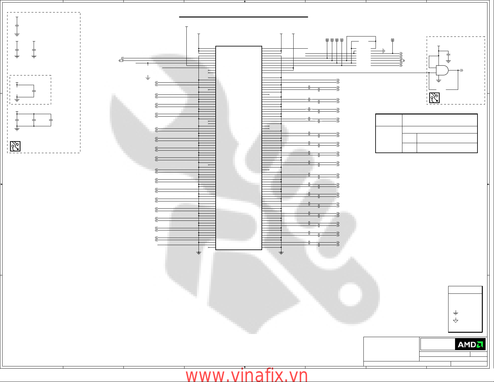
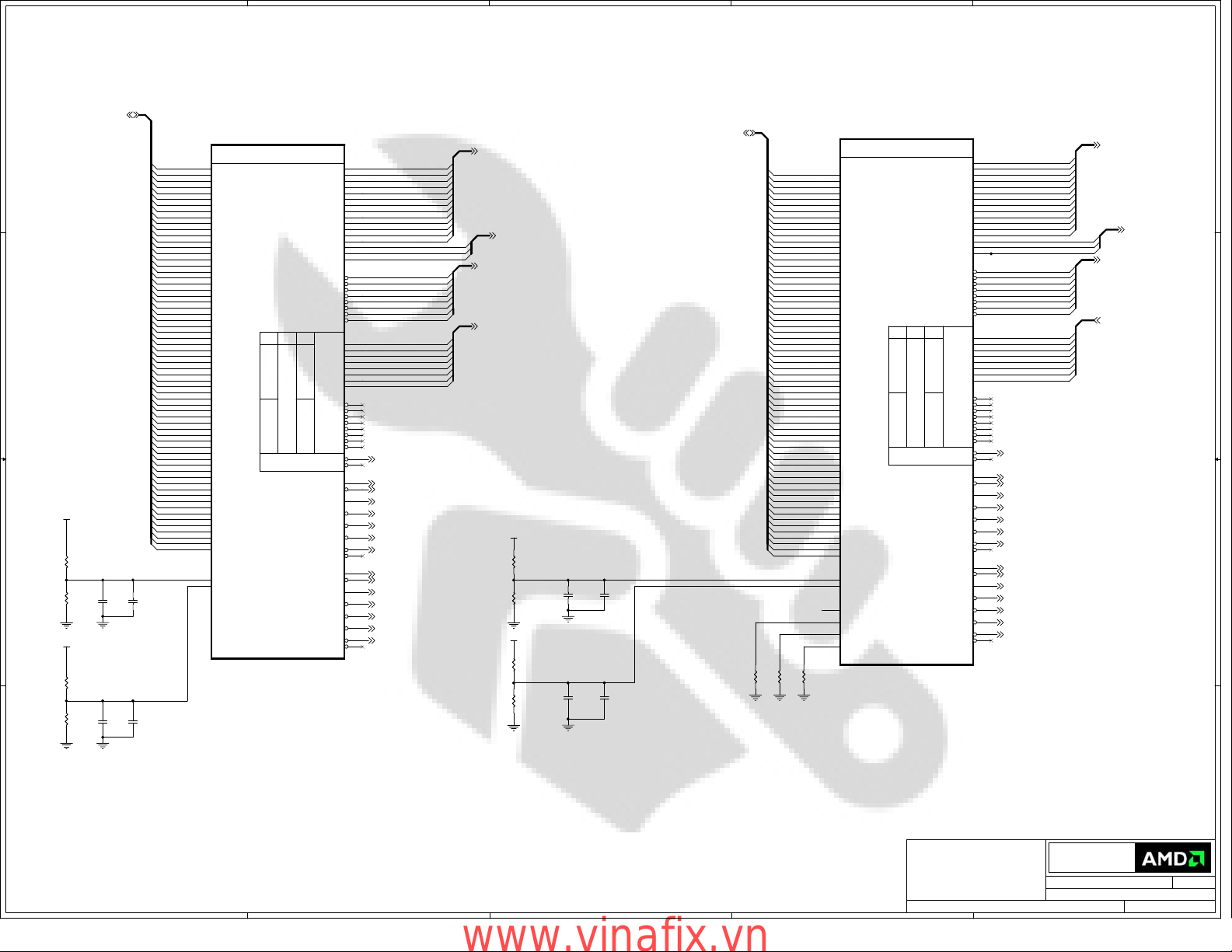
PCI-EXPRESS EDGE CONNECTOR
+3.3V_BUS
+12V_BUS
B1
B2
B3
B4
B5
B6
B7
B8
B9
B10
B11
B12
B13
B14
B15
B16
B17
B18
B19
B20
B21
B22
B23
B24
B25
B26
B27
B28
B29
B30
B31
B32
B33
B34
B35
B36
B37
B38
B39
B40
B41
B42
B43
B44
B45
B46
B47
B48
B49
B50
B51
B52
B53
B54
B55
B56
B57
B58
B59
B60
B61
B62
B63
B64
B65
B66
B67
B68
B69
B70
B71
B72
B73
B74
B75
B76
B77
B78
B79
B80
B81
B82
+12V#B1
+12V#B2
+12V#B3
GND#B4
SMCLK
SMDAT
GND#B7
+3.3V#B8
JTAG1
3.3Vaux
WAKE#
RSVD#B12
GND#B13
PETp0
PETn0
GND#B16
PRSNT2#B17
GND#B18
PETp1
PETn1
GND#B21
GND#B22
PETp2
PETn2
GND#B25
GND#B26
PETp3
PETn3
GND#B29
RSVD#B30
PRSNT2#B31
GND#B32
PETp4
PETn4
GND#B35
GND#B36
PETp5
PETn5
GND#B39
GND#B40
PETp6
PETn6
GND#B43
GND#B44
PETp7
PETn7
GND#B47
PRSNT2#B48
GND#B49
PETp8
PETn8
GND#B52
GND#B53
PETp9
PETn9
GND#B56
GND#B57
PETp10
PETn10
GND#B60
GND#B61
PETp11
PETn11
GND#B64
GND#B65
PETp12
PETn12
GND#B68
GND#B69
PETp13
PETn13
GND#B72
GND#B73
PETp14
PETn14
GND#B76
GND#B77
PETp15
PETn15
GND#B80
PRSNT2#B81
RSVD#B82
x16 PCIe
x16 PCIe
Mechanical Key
Mechanical Key
PRSNT1#A1
+12V#A2
+12V#A3
GND#A4
JTAG2
JTAG3
JTAG4
JTAG5
+3.3V#A9
+3.3V#A10
PERST#
GND#A12
REFCLK+
REFCLKGND#A15
PERp0
PERn0
GND#A18
RSVD#A19
GND#A20
PERp1
PERn1
GND#A23
GND#A24
PERp2
PERn2
GND#A27
GND#A28
PERp3
PERn3
GND#A31
RSVD#A32
RSVD#A33
GND#A34
PERp4
PERn4
GND#A37
GND#A38
PERp5
PERn5
GND#A41
GND#A42
PERp6
PERn6
GND#A45
GND#A46
PERp7
PERn7
GND#A49
RSVD#A50
GND#A51
PERp8
PERn8
GND#A54
GND#A55
PERp9
PERn9
GND#A58
GND#A59
PERp10
PERn10
GND#A62
GND#A63
PERp11
PERn11
GND#A66
GND#A67
PERp12
PERn12
GND#A70
GND#A71
PERp13
PERn13
GND#A74
GND#A75
PERp14
PERn14
GND#A78
GND#A79
PERp15
PERn15
GND#A82
MPCIE1
MPCIE1
A1
A2
A3
A4
A5
A6
A7
A8
A9
A10
A11
A12
A13
A14
A15
A16
A17
A18
A19
A20
A21
A22
A23
A24
A25
A26
A27
A28
A29
A30
A31
A32
A33
A34
A35
A36
A37
A38
A39
A40
A41
A42
A43
A44
A45
A46
A47
A48
A49
A50
A51
A52
A53
A54
A55
A56
A57
A58
A59
A60
A61
A62
A63
A64
A65
A66
A67
A68
A69
A70
A71
A72
A73
A74
A75
A76
A77
A78
A79
A80
A81
A82
PERp0
PERn0
PERp1
PERn1
PERp2
PERn2
PERp3
PERn3
PERp4
PERn4
PERp5
PERn5
PERp6
PERn6
PERp7
PERn7
PERp8
PERn8
PERp9
PERn9
PERp10
PERn10
PERp11
PERn11
PERp12
PERn12
PERp13
PERn13
PERp14
PERn14
PERp15
PERn15
+3.3V_BUS+12V_BUS
PRESENCE
JTCK
JTDI
JTDO
JTMS
TEST_EN_J
JTAG_TRST#
C7
100nF_6.3VC7100nF_6.3V
C9
100nF_6.3VC9100nF_6.3V
C11
C11
100nF_6.3V
100nF_6.3V
C13
C13
100nF_6.3V
100nF_6.3V
C15
C15
100nF_6.3V
100nF_6.3V
C17
C17
100nF_6.3V
100nF_6.3V
C19
C19
100nF_6.3V
100nF_6.3V
C21
C21
100nF_6.3V
100nF_6.3V
C23
C23
100nF_6.3V
100nF_6.3V
C25
C25
100nF_6.3V
100nF_6.3V
C27
C27
100nF_6.3V
100nF_6.3V
C29
C29
100nF_6.3V
100nF_6.3V
C31
C31
100nF_6.3V
100nF_6.3V
C33
C33
100nF_6.3V
100nF_6.3V
C35
C35
100nF_6.3V
100nF_6.3V
C37
C37
100nF_6.3V
100nF_6.3V
PERST#
TP3TP3
TP4TP4
C8
100nF_6.3VC8100nF_6.3V
C10
C10
100nF_6.3V
100nF_6.3V
C12
C12
100nF_6.3V
100nF_6.3V
C14
C14
100nF_6.3V
100nF_6.3V
C16
C16
100nF_6.3V
100nF_6.3V
C18
C18
100nF_6.3V
100nF_6.3V
C20
C20
100nF_6.3V
100nF_6.3V
C22
C22
100nF_6.3V
100nF_6.3V
C24
C24
100nF_6.3V
100nF_6.3V
C26
C26
100nF_6.3V
100nF_6.3V
C28
C28
100nF_6.3V
100nF_6.3V
C30
C30
100nF_6.3V
100nF_6.3V
C32
C32
100nF_6.3V
100nF_6.3V
C34
C34
100nF_6.3V
100nF_6.3V
C36
C36
100nF_6.3V
100nF_6.3V
C38
C38
100nF_6.3V
100nF_6.3V
TP2TP2
TP1TP1
PCIE_REFCLKP (2)
PCIE_REFCLKN (2)PETp0_GFXRp0(2)
GFXTp0_PERp0 (2)
GFXTn0_PERn0 (2)
GFXTp1_PERp1 (2)
GFXTn1_PERn1 (2)
GFXTp2_PERp2 (2)
GFXTn2_PERn2 (2)
GFXTp3_PERp3 (2)
GFXTn3_PERn3 (2)
GFXTp4_PERp4 (2)
GFXTn4_PERn4 (2)
GFXTp5_PERp5 (2)
GFXTn5_PERn5 (2)
GFXTp6_PERp6 (2)
GFXTn6_PERn6 (2)
GFXTp7_PERp7 (2)
GFXTn7_PERn7 (2)
GFXTp8_PERp8 (2)
GFXTn8_PERn8 (2)
GFXTp9_PERp9 (2)
GFXTn9_PERn9 (2)
GFXTp10_PERp10 (2)
GFXTn10_PERn10 (2)
GFXTp11_PERp11 (2)
GFXTn11_PERn11 (2)
GFXTp12_PERp12 (2)
GFXTn12_PERn12 (2)
GFXTp13_PERp13 (2)
GFXTn13_PERn13 (2)
GFXTp14_PERp14 (2)
GFXTn14_PERn14 (2)
GFXTp15_PERp15 (2)
GFXTn15_PERn15 (2)
No JTAG
TP6TP6
TEST_EN_R (3)
HSYNC1_TRST (3)
VSYNC1_TCK (3)
GEN_D_HPD4_TDO (7)
DDC1CLK_TMS (3)
+3.3V
53
1
2
R_RST
Place R3 in U5
Table 1: Connection for JTAG
Production
(No JTAG)
Internal Use Only
TSW1 & R2 are located on the bottom side of the board close to PCIE connector.
Install R1 & R2 .Don't Install TSW1
Install TSW1 & Don't Install R2
TSW1 Switch #1, 2, 3, 4, 5 and 6 closed (ON)
JTAG
#7,8 open
TSW1 Switch #1, 2, 3, 4, 5 and 6 open
NO JTAG
#7,8 closed (ON)
C39
C39
100nF_6.3V
100nF_6.3V
NC7SZ08P5X_NL
NC7SZ08P5X_NL
4
U5
U5
PERST#_buf (2)
SYMBOL LEGEND
DO NOT
DNI
INSTALL
#
ACTIVE
LOW
DIGITAL
GROUND
ANALOG
A A
CONFIDENTIAL & PROPRIETARY TO ADVANCED MICRO DEVICES INC.
CONFIDENTIAL & PROPRIETARY TO ADVANCED MICRO DEVICES INC.
CONFIDENTIAL & PROPRIETARY TO ADVANCED MICRO DEVICES INC.
© 2007 Advanced Micro Devices
© 2007 Advanced Micro Devices
© 2007 Advanced Micro Devices
This AMD Board schematic and design is the exclusive property of AMD,
This AMD Board schematic and design is the exclusive property of AMD,
This AMD Board schematic and design is the exclusive property of AMD,
and is provided only to entities under a non-disclosure agreement
and is provided only to entities under a non-disclosure agreement
and is provided only to entities under a non-disclosure agreement
with AMD for evaluation purposes. Further distribution or disclosure
with AMD for evaluation purposes. Further distribution or disclosure
with AMD for evaluation purposes. Further distribution or disclosure
is strictly prohibited. Use of this schematic and design for any purpose
is strictly prohibited. Use of this schematic and design for any purpose
is strictly prohibited. Use of this schematic and design for any purpose
other than evaluation requires a Board Technology License Agreement
other than evaluation requires a Board Technology License Agreement
other than evaluation requires a Board Technology License Agreement
with AMD. AMD makes no representations or warranties of any kind
with AMD. AMD makes no representations or warranties of any kind
with AMD. AMD makes no representations or warranties of any kind
regarding this schematic and design, including, not limited to,
regarding this schematic and design, including, not limited to,
regarding this schematic and design, including, not limited to,
any implied warranty of merchantibility or fitness for a particular
any implied warranty of merchantibility or fitness for a particular
any implied warranty of merchantibility or fitness for a particular
purpose, and disclaims responsibility forany consequences resulting
purpose, and disclaims responsibility forany consequences resulting
purpose, and disclaims responsibility forany consequences resulting
from use of the information included herein.
from use of the information included herein.
from use of the information included herein.
Title
Title
Title
RV635 DDR2 - PCI-E Edge Connector
RV635 DDR2 - PCI-E Edge Connector
8
7
6
5
4
3
RV635 DDR2 - PCI-E Edge Connector
2
Advanced Micro Devices Inc.
Advanced Micro Devices Inc.
Advanced Micro Devices Inc.
1 Commerce Valley Drive East
1 Commerce Valley Drive East
1 Commerce Valley Drive East
Markham, Ontario
Markham, Ontario
Markham, Ontario
Thursday, January 24, 2008
Thursday, January 24, 2008
Thursday, January 24, 2008
Sheet
Sheet
Sheet
of
120
of
120
of
120
GROUND
BUO BRING UP
ONLY
Doc No.
Doc No.
Doc No.
102-B38101-00
102-B38101-00
102-B38101-00
1
RevDate:
RevDate:
RevDate:
13
13
13
www.vinafix.vn
Page 2
5
D D
NOTE: some of the PCIE testpoints will
be available trought via on traces.
PETp0_GFXRp0(1)
PETn0_GFXRn0(1)
PETp1_GFXRp1(1)
PETn1_GFXRn1(1)
PETp2_GFXRp2(1)
PETn2_GFXRn2(1)
PETp3_GFXRp3(1)
PETn3_GFXRn3(1)
PETp4_GFXRp4(1)
PETn4_GFXRn4(1)
PETp5_GFXRp5(1)
PETn5_GFXRn5(1)
PETp6_GFXRp6(1)
C C
B B
PCIE_REFCLKP(1)
PCIE_REFCLKN(1)
PETn6_GFXRn6(1)
PETp7_GFXRp7(1)
PETn7_GFXRn7(1)
PETp8_GFXRp8(1)
PETp9_GFXRp9(1)
PETn9_GFXRn9(1)
PETp10_GFXRp10(1)
PETn10_GFXRn10(1)
PETp11_GFXRp11(1)
PETn11_GFXRn11(1)
PETp12_GFXRp12(1)
PETn12_GFXRn12(1)
PETp13_GFXRp13(1)
PETn13_GFXRn13(1)
PETp14_GFXRp14(1)
PETn14_GFXRn14(1)
PETp15_GFXRp15(1)
PETn15_GFXRn15(1)
DNI DNI
402 402
TP11TP11
TP12TP12
TP13TP13
TP14TP14
TP19TP19
TP20TP20
TP21TP21
TP22TP22
TP27TP27
TP28TP28
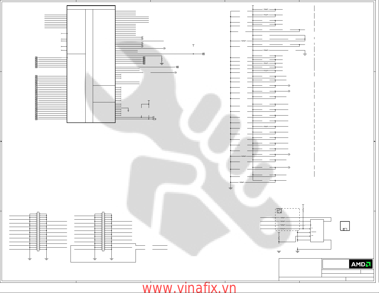
4
U1A
TP7TP7
TP8TP8
TP9TP9
TP10TP10
TP15TP15
TP16TP16
TP17TP17
TP18TP18
TP23TP23
TP24TP24
TP25TP25
TP26TP26
U1A
AK33
AJ33
AJ35
AJ34
AH35
AH34
AG35
AG34
AF33
AE33
AE35
AE34
AD35
AD34
AC35
AC34
AB33
AA33
AA35
AA34
Y35
Y34
W35
W34
V33
U33
U35
U34
T35
T34
R35
R34
AJ31
AJ30
PERST#_buf(1)
AM32
PCIE_RX0P
PCIE_RX0N
PCIE_RX1P
PCIE_RX1N
PCIE_RX2P
PCIE_RX2N
PCIE_RX3P
PCIE_RX3N
PCIE_RX4P
PCIE_RX4N
PCIE_RX5P
PCIE_RX5N
PCIE_RX6P
PCIE_RX6N
PCIE_RX7P
PCIE_RX7N
PCIE_RX8P
PCIE_RX8N
PCIE_RX9P
PCIE_RX9N
PCIE_RX10P
PCIE_RX10N
PCIE_RX11P
PCIE_RX11N
PCIE_RX12P
PCIE_RX12N
PCIE_RX13P
PCIE_RX13N
PCIE_RX14P
PCIE_RX14N
PCIE_RX15P
PCIE_RX15N
Clock
Clock
PCIE_REFCLKP
PCIE_REFCLKN
PERSTB
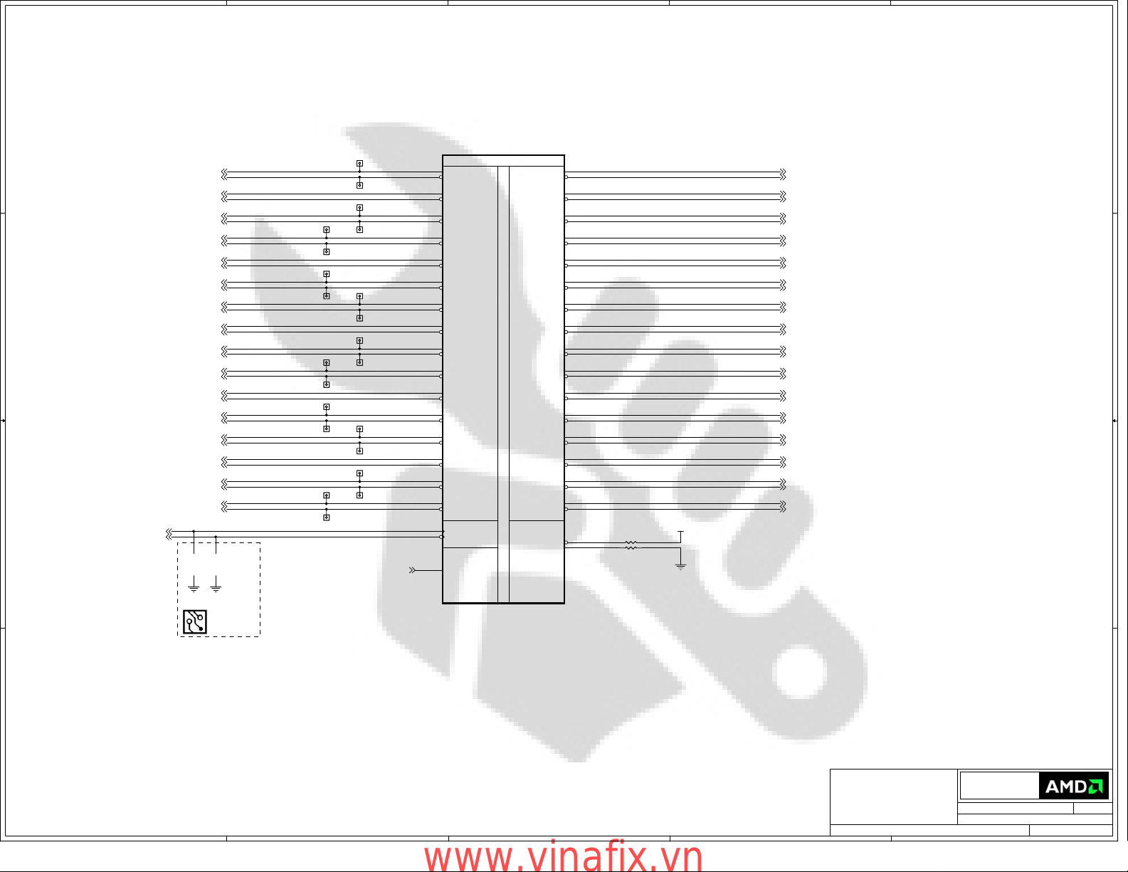
PART 1 OF 7
PART 1 OF 7
P
P
C
C
I
I
-
E
E
X
X
P
P
R
R
E
E
S
S
S
S
I
I
N
N
T
T
E
E
R
R
F
F
A
A
C
C
E
E
PCIE_TX0P
PCIE_TX0N
PCIE_TX1P
PCIE_TX1N
PCIE_TX2P
PCIE_TX2N
PCIE_TX3P
PCIE_TX3N
PCIE_TX4P
PCIE_TX4N
PCIE_TX5P
PCIE_TX5N
PCIE_TX6P
PCIE_TX6N
PCIE_TX7P
PCIE_TX7N
PCIE_TX8P
PCIE_TX8N
PCIE_TX9P
PCIE_TX9N
PCIE_TX10P
PCIE_TX10N
PCIE_TX11P
PCIE_TX11N
PCIE_TX12P
PCIE_TX12N
PCIE_TX13P
PCIE_TX13N
PCIE_TX14P
PCIE_TX14N
PCIE_TX15P
PCIE_TX15N
Calibration
Calibration
PCIE_CALRN
PCIE_CALRP
3
AG31
AG30
AF31
AF30
AF28
AF27
AD31
AD30
AD28
AD27
AB31
AB30
AB28
AB27
AA31
AA30
AA28
AA27
W31
W30
W28
W27
V31
V30
V28
V27
U31
U30
U28
U27
R31
R30
+PCIE_VDDC
402
AG26
AJ27
R9
1.27KR91.27K
R82.0K R82.0K
402
2
GFXTp0_PERp0 (1)
GFXTn0_PERn0 (1)
GFXTp1_PERp1 (1)
GFXTn1_PERn1 (1)
GFXTp2_PERp2 (1)
GFXTn2_PERn2 (1)
GFXTp3_PERp3 (1)
GFXTn3_PERn3 (1)
GFXTp4_PERp4 (1)
GFXTn4_PERn4 (1)
GFXTp5_PERp5 (1)
GFXTn5_PERn5 (1)
GFXTp6_PERp6 (1)
GFXTn6_PERn6 (1)
GFXTp7_PERp7 (1)
GFXTn7_PERn7 (1)
GFXTp8_PERp8 (1)
GFXTn8_PERn8 (1)PETn8_GFXRn8(1)
GFXTp9_PERp9 (1)
GFXTn9_PERn9 (1)
GFXTp10_PERp10 (1)
GFXTn10_PERn10 (1)
GFXTp11_PERp11 (1)
GFXTn11_PERn11 (1)
GFXTp12_PERp12 (1)
GFXTn12_PERn12 (1)
GFXTp13_PERp13 (1)
GFXTn13_PERn13 (1)
GFXTp14_PERp14 (1)
GFXTn14_PERn14 (1)
GFXTp15_PERp15 (1)
GFXTn15_PERn15 (1)
1
For Tektronix LA only
Place close
to ASIC
A A
5
4
RV635 PRO A11
RV635 PRO A11
CONFIDENTIAL & PROPRIETARY TO ADVANCED MICRO DEVICES INC.
CONFIDENTIAL & PROPRIETARY TO ADVANCED MICRO DEVICES INC.
CONFIDENTIAL & PROPRIETARY TO ADVANCED MICRO DEVICES INC.
© 2007 Advanced Micro Devices
© 2007 Advanced Micro Devices
© 2007 Advanced Micro Devices
This AMD Board schematic and design is the exclusive property of AMD,
This AMD Board schematic and design is the exclusive property of AMD,
This AMD Board schematic and design is the exclusive property of AMD,
and is provided only to entities under a non-disclosure agreement
and is provided only to entities under a non-disclosure agreement
and is provided only to entities under a non-disclosure agreement
with AMD for evaluation purposes. Further distribution or disclosure
with AMD for evaluation purposes. Further distribution or disclosure
with AMD for evaluation purposes. Further distribution or disclosure
is strictly prohibited. Use of this schematic and design for any purpose
is strictly prohibited. Use of this schematic and design for any purpose
is strictly prohibited. Use of this schematic and design for any purpose
other than evaluation requires a Board Technology License Agreement
other than evaluation requires a Board Technology License Agreement
other than evaluation requires a Board Technology License Agreement
with AMD. AMD makes no representations or warranties of any kind
with AMD. AMD makes no representations or warranties of any kind
with AMD. AMD makes no representations or warranties of any kind
regarding this schematic and design, including, not limited to,
regarding this schematic and design, including, not limited to,
regarding this schematic and design, including, not limited to,
any implied warranty of merchantibility or fitness for a particular
any implied warranty of merchantibility or fitness for a particular
any implied warranty of merchantibility or fitness for a particular
purpose, and disclaims responsibility forany consequences resulting
purpose, and disclaims responsibility forany consequences resulting
purpose, and disclaims responsibility forany consequences resulting
from use of the information included herein.
from use of the information included herein.
from use of the information included herein.
Title
Title
Title
RV635 DDR2 - ASIC PCIE_Interface
RV635 DDR2 - ASIC PCIE_Interface
3
2
RV635 DDR2 - ASIC PCIE_Interface
Advanced Micro Devices Inc.
Advanced Micro Devices Inc.
Advanced Micro Devices Inc.
1 Commerce Valley Drive East
1 Commerce Valley Drive East
1 Commerce Valley Drive East
Markham, Ontario
Markham, Ontario
Markham, Ontario
Thursday, January 24, 2008
Thursday, January 24, 2008
Thursday, January 24, 2008
Sheet
Sheet
Sheet
of
220
of
220
of
220
1
Doc No.
Doc No.
Doc No.
RevDate:
RevDate:
RevDate:
13
13
13
102-B38101-00
102-B38101-00
102-B38101-00
www.vinafix.vn
Page 3
5
Recommended caps:
(see BOM for qualified values/vendors)
10uF , X6S, 0805, 6.3V, 1.4MM MAX THICK
1uF, X6S, 0402, 6.3V
100nF, X7R, 0402
10nF , X7R, 0402
Overlap footprints
4.7uF_6.3V
4.7uF_6.3V
R1090RR109
0R
DNI
Place close to ASIC
MC100
MC100
4.7uF_6.3V
4.7uF_6.3V
GND_T2PVSS
MC103
MC103
+LTVDD33
+3.3V
R40
R40
4.7K
4.7K
402 402
1uF_6.3V
1uF_6.3V
1uF_6.3V
1uF_6.3V
DDC1DATA_TDI(1)
R41
R41
4.7K
4.7K
DDC2DATA
DDC2CLK
SDA
SCL
+1.8V
Share one pad
R85 0RR85 0R
R841MR84
1M
MR86 0RMR86 0R
Place R_RTCLK close to XTAL so the
main clock line has shortest stub
C108
C108
C107
C107
R43 221RR43 221R
R44 110RR44 110R
OSC_EN
R_RTCLK
100nF_6.3V
100nF_6.3V
CRT1DDCDATA(15)
CRT1DDCCLK(15)
DNI
C101
C101
C109
C109
100nF_6.3V
100nF_6.3V
C46
C46
100nF_6.3V
100nF_6.3V
+LTVDD18
C105
C105
100nF_6.3V
100nF_6.3V
GPU_DMINUS(18)
GPU_DPLUS(18)
TS_FDO(18)
TP42
TP42
35mil
35mil
PLL_TEST
TEST_EN
D D
+1.8V
B889
B889
BLM15BD121SN1
BLM15BD121SN1
C C
LVT_EN(13)
I2C DEVICE ADDRESS' ON DDC2
B B
DEVICE
LM63
DP
+1.8V
+3.3V
R35
R35
4.7K
4.7K
ADDRESS
x100 1100
TBD
+T2PVDD
Q100
Q100
SI2304DS
SI2304DS
1
T2XCM(15)
T2XCP(15)
T2X0M(15)
T2X0P(15)
T2X1M(15)
T2X1P(15)
T2X2M(15)
T2X2P(15)
T2X3M(15)
T2X3P(15)
T2X4M(15)
T2X4P(15)
T2X5M(15)
T2X5P(15)
NS100
NS100
NS_VIA
NS_VIA
1 2
Use 0R
B1000RB100
32
0R
DDC2DATA(13,18)
DDC2CLK(13,18)
DDC3_DATA_DP3_AUXN(16)
DDC3_CLK_DP3_AUXP(16)
DDC4_DATA_DP4_AUXN(17)
DDC4_CLK_DP4_AUXP(17)
R36
R36
DDC1CLK_TMS(1)
4.7K
4.7K
What happens to all the JTAG resistors especially R7 and also the TRs?
Do Not Share PADs
TEST_EN_R(1)
XTALOUT_S
Y82
Y82
27.000MHz_10PPM
27.000MHz_10PPM
XTALOUT_S
is done for
ease of layout
5
XTALIN_S
XTALOUT_S
+3.3V_BUS
A A
C82
C82
10pF_50V
10pF_50V
2 1
C83
C83
10pF_50V
10pF_50V
HPD1(16)
T2XCM
T2XCP
T2X0M
T2X0P
T2X1M
T2X1P
T2X2M
T2X2P
T2X3M
T2X3P
T2X4M
T2X4P
T2X5M
T2X5P
C102
C102
1uF_6.3V
1uF_6.3V
DNI
VREFG
XTALIN
XTALOUT
4
AP22
AR22
AN22
AN23
AR23
AP23
AR24
AP24
AR25
AP25
AN26
AN27
AR27
AP27
AL22
AK22
AK27
AL27
AJ26
AH26
AJ22
AN21
AN24
AN25
AN28
AP21
AP26
AR21
AR26
AJ24
AM22
AM24
AM26
AM27
AM29
AL29
AJ15
AH15
AJ5
AJ4
AH14
AG14
AG6
AK6
AM6
AK4
AM4
AG21
AH19
AM30
AD12
AR33
AP33
Share one pad
OSC_EN (13,14)
4
U1B
U1B
Integrated
Integrated
LVTM/TMDS2
LVTM/TMDS2
T2XCM
T2XCP
T2X0M
T2X0P
T2X1M
T2X1P
T2X2M
T2X2P
T2X3M
T2X3P
T2X4M
T2X4P
T2X5M
T2X5P
T2PVDD
T2PVSS
T2XVDDC_1
T2XVDDC_2
T2XVDDR_1
T2XVDDR_2
T2XVSSR_1
T2XVSSR_2
T2XVSSR_3
T2XVSSR_4
T2XVSSR_5
T2XVSSR_6
T2XVSSR_7
T2XVSSR_8
T2XVSSR_9
T2XVSSR_10
T2XVSSR_11
T2XVSSR_12
T2XVSSR_13
T2XVSSR_14
Monitor
Monitor
DDC1DATA
Interface
Interface
DDC1CLK
DDC2DATA
DDC2CLK
DDC3DATA_DP3_AUXN
DDC3CLK_DP3_AUXP
DDC4DATA_DP4_AUXN
DDC4CLK_DP4_AUXP
HPD1
SDA
MMI2C
MMI2C
SCL
DMINUS
Thermal
Thermal
DPLUS
Diode
Diode
TS_FDO
PLLTEST
Test
Test
TESTEN
VREFG
XTALIN
XTALOUT
RV635 PRO A11
RV635 PRO A11
PART 2 OF 7
PART 2 OF 7
V
V
I
I
D
D
E
E
O
O
&
&
M
M
U
U
L
L
T
T
I
I
M
M
E
E
D
D
I
I
A
A
Integrated
Integrated
DP/TMDS
DP/TMDS
TXCAM_DPA3N
TXCAP_DPA3P
TX0M_DPA2N
TX0P_DPA2P
TX1M_DPA1N
TX1P_DPA1P
TX2M_DPA0N
TX2P_DPA0P
TXCBM_DPB3N
TXCBP_DPB3P
TX3M_DPB2N
TX3P_DPB2P
TX4M_DPB1N
TX4P_DPB1P
TX5M_DPB0N
TX5P_DPB0P
DPA_PVDD
DPA_PVSS
DPB_PVDD
DPB_PVSS
DPA_VDDR_1
DPA_VDDR_2
DPA_VSSR_1
DPA_VSSR_2
DPA_VSSR_3
DPA_VSSR_4
DPA_VSSR_5
DPB_VDDR_1
DPB_VDDR_2
DPB_VSSR_1
DPB_VSSR_2
DPB_VSSR_3
DPB_VSSR_4
DPB_VSSR_5
DAC / CRT
DAC / CRT
DAC2 (TV/CRT2)
DAC2 (TV/CRT2)
DP_CALR
HSYNC
VSYNC
RSET
AVDD
AVSSQ
VDD1DI
VSS1DI
H2SYNC
V2SYNC
COMP
R2SET
A2VDDQ
A2VSSQ
VDD2DI
VSS2DI
A2VDD
AN9
AN10
AR10
AP10
AR11
AP11
AR12
AP12
AR14
AP14
AR15
AP15
AR16
AP16
AR17
AP17
DP_CALR
AG15
AM14
AL14
AH17
AG17
AP19
AR19
AN11
AN12
AN13
AN14
AN15
AN19
AN20
AN16
AN17
AN18
AR18
AP18
AR31
R
AP31
RB
AR30
G
AP30
GB
AR29
B
AP29
BB
AN29
AN30
AN31
AR32
AP32
AR28
AP28
AM19
R2
AL19
R2B
AM18
G2
AL18
G2B
AM17
B2
AL17
B2B
AM15
AL15
AK18
Y
AK19
C
AK17
R2SET GND_A2VSSQ
AJ21
AL21
AK21
AH22
AG22
AM21
C2030
C2030
10nF
10nF
3
R128 150RR128 150R
GND_DPAVSS
GND_DBPVSS
R1030 499RR1030 499R
C1023
C1023
10nF
10nF
R2030 715RR2030 715R
C2021
C2021
100nF_6.3V
100nF_6.3V
C2024
C2024
10nF
10nF
C2031
C2031
100nF_6.3V
100nF_6.3V
3
DPA_C_3N
DPA_C_3P
DPA_C_2N
DPA_C_2P
DPA_C_1N
DPA_C_1P
DPA_C_0N
DPA_C_0P
DPB_C_3N
DPB_C_3P
DPB_C_2N
DPB_C_2P
DPB_C_1N
DPB_C_1P
DPB_C_0N
DPB_C_0P
C111
C111
100nF
100nF
C190
C190
100nF
100nF
C115
C115
100nF
100nF
C193
C193
100nF
100nF
C2025
C2025
100nF_6.3V
100nF_6.3V
GND_AVSSQRSET
C1024
C1024
100nF_6.3V
100nF_6.3V
C2032
C2032
1uF_6.3V
1uF_6.3V
C112
C112
1uF_6.3V
1uF_6.3V
C191
C191
1uF_6.3V
1uF_6.3V
C116
C116
1uF_6.3V
1uF_6.3V
C194
C194
1uF_6.3V
1uF_6.3V
C2022
C2022
1uF_6.3V
1uF_6.3V
+VDD2DI
C2026
C2026
1uF_6.3V
1uF_6.3V
GND_VSS2DI
C1025
C1025
1uF_6.3V
1uF_6.3V
Overlap footprints
Place close to Connector
C1127 100nF_6.3VC1127 100nF_6.3V
C1126 100nF_6.3VC1126 100nF_6.3V
C1125 100nF_6.3VC1125 100nF_6.3V
C1124 100nF_6.3VC1124 100nF_6.3V
C1123 100nF_6.3VC1123 100nF_6.3V
C1122 100nF_6.3VC1122 100nF_6.3V
C1121 100nF_6.3VC1121 100nF_6.3V
C1120 100nF_6.3VC1120 100nF_6.3V
C1137 100nF_6.3VC1137 100nF_6.3V
C1136 100nF_6.3VC1136 100nF_6.3V
C1135 100nF_6.3VC1135 100nF_6.3V
C1134 100nF_6.3VC1134 100nF_6.3V
C1133 100nF_6.3VC1133 100nF_6.3V
C1132 100nF_6.3VC1132 100nF_6.3V
C1131 100nF_6.3VC1131 100nF_6.3V
C1130 100nF_6.3VC1130 100nF_6.3V
Overlap footprints
MC113
MC113
4.7uF_6.3V
4.7uF_6.3V
Overlap footprints
MC192
MC192
4.7uF_6.3V
4.7uF_6.3V
Overlap footprints
MC117
MC117
4.7uF_6.3V
4.7uF_6.3V
Overlap footprints
MC195
MC195
4.7uF_6.3V
4.7uF_6.3V
C1020
C1020
C1021
C1021
10nF
10nF
100nF_6.3V
100nF_6.3V
+VDD1DI
NS1021 NS_VIANS1021 NS_VIA
GND_VSS1DI
+A2VDDQ
NS2020 NS_VIANS2020 NS_VIA
NS2021 NS_VIANS2021 NS_VIA
12
MC2033
MC2033
4.7uF_6.3V
4.7uF_6.3V
C1022
C1022
1uF_6.3V
1uF_6.3V
12
GND_A2VSSQ
12
+A2VDD
2
+DPA_PVDD
+DPB_PVDD
+DPA_VDDR
+DPB_VDDR
+AVDD
NS1020 NS_VIANS1020 NS_VIA
B887 BLM15BD121SN1B887 BLM15BD121SN1
NS110
NS110
NS_VIA
NS_VIA
12
B890 BLM15BD121SN1B890 BLM15BD121SN1
NS190
NS190
NS_VIA
NS_VIA
12
B881 BLM15BD121SN1B881 BLM15BD121SN1
B892 BLM15BD121SN1B892 BLM15BD121SN1
A_DAC1_R (15)
A_DAC1_RB (15)
A_DAC1_G (15)
A_DAC1_GB (15)
A_DAC1_B (15)
A_DAC1_BB (15) HSYNC1_TRST (1)
12
GND_AVSSQ
A_DAC2_R (16)
A_DAC2_RB (16)
A_DAC2_G (16)
A_DAC2_GB (16)
A_DAC2_B (16)
A_DAC2_BB (16)
HSYNC_DAC2 (7,16)
VSYNC_DAC2 (7,16)
B2030 26R_600mAB2030 26R_600mA
+3.3V
Title
Title
2
Title
+1.8V
+1.8V
+1.1V
+1.1V
DNI
DNI
+1.8V
B884
B884
BLM15BD121SN1
BLM15BD121SN1
+1.8V
B883
B883
BLM15BD121SN1
BLM15BD121SN1
+1.8V
B885
B885
BLM15BD121SN1
BLM15BD121SN1
CONFIDENTIAL & PROPRIETARY TO ADVANCED MICRO DEVICES INC.
CONFIDENTIAL & PROPRIETARY TO ADVANCED MICRO DEVICES INC.
CONFIDENTIAL & PROPRIETARY TO ADVANCED MICRO DEVICES INC.
© 2007 Advanced Micro Devices
© 2007 Advanced Micro Devices
© 2007 Advanced Micro Devices
This AMD Board schematic and design is the exclusive property of AMD,
This AMD Board schematic and design is the exclusive property of AMD,
This AMD Board schematic and design is the exclusive property of AMD,
and is provided only to entities under a non-disclosure agreement
and is provided only to entities under a non-disclosure agreement
and is provided only to entities under a non-disclosure agreement
with AMD for evaluation purposes. Further distribution or disclosure
with AMD for evaluation purposes. Further distribution or disclosure
with AMD for evaluation purposes. Further distribution or disclosure
is strictly prohibited. Use of this schematic and design for any purpose
is strictly prohibited. Use of this schematic and design for any purpose
is strictly prohibited. Use of this schematic and design for any purpose
other than evaluation requires a Board Technology License Agreement
other than evaluation requires a Board Technology License Agreement
other than evaluation requires a Board Technology License Agreement
with AMD. AMD makes no representations or warranties of any kind
with AMD. AMD makes no representations or warranties of any kind
with AMD. AMD makes no representations or warranties of any kind
regarding this schematic and design, including, not limited to,
regarding this schematic and design, including, not limited to,
regarding this schematic and design, including, not limited to,
any implied warranty of merchantibility or fitness for a particular
any implied warranty of merchantibility or fitness for a particular
any implied warranty of merchantibility or fitness for a particular
purpose, and disclaims responsibility forany consequences resulting
purpose, and disclaims responsibility forany consequences resulting
purpose, and disclaims responsibility forany consequences resulting
from use of the information included herein.
from use of the information included herein.
from use of the information included herein.
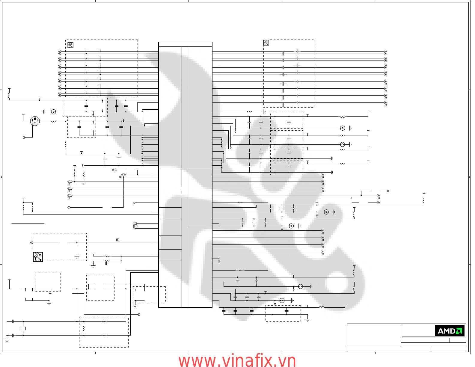
RV635 DDR2 - ASIC MAIN
RV635 DDR2 - ASIC MAIN
RV635 DDR2 - ASIC MAIN
DPA_3N (16)
DPA_3P (16)
DPA_2N (16)
DPA_2P (16)
DPA_1N (16)
DPA_1P (16)
DPA_0N (16)
DPA_0P (16)
DPB_3N (17)
DPB_3P (17)
DPB_2N (17)
DPB_2P (17)
DPB_1N (17)
DPB_1P (17)
DPB_0N (17)
DPB_0P (17)
HSYNC_DAC1 (7,15)
VSYNC_DAC1 (7,15)
VSYNC1_TCK (1)
1
+1.8V
Advanced Micro Devices Inc.
Advanced Micro Devices Inc.
Advanced Micro Devices Inc.
1 Commerce Valley Drive East
1 Commerce Valley Drive East
1 Commerce Valley Drive East
Markham, Ontario
Markham, Ontario
Markham, Ontario
Thursday, January 24, 2008
Thursday, January 24, 2008
Thursday, January 24, 2008
Sheet
Sheet
Sheet
of
320
of
320
of
320
1
B882
B882
BLM15BD121SN1
BLM15BD121SN1
Doc No.
Doc No.
Doc No.
RevDate:
RevDate:
RevDate:
13
13
13
102-B38101-00
102-B38101-00
102-B38101-00
www.vinafix.vn
Page 4
C151
C151
1uF_6.3V
1uF_6.3V
C131
C131
100nF_6.3V
100nF_6.3V
C141
C141
1uF_6.3V
1uF_6.3V
5
C152
C152
1uF_6.3V
1uF_6.3V
C132
C132
100nF_6.3V
100nF_6.3V
C142
C142
1uF_6.3V
1uF_6.3V
C133
C133
100nF_6.3V
100nF_6.3V
C143
C143
1uF_6.3V
1uF_6.3V
C154
C154
1uF_6.3V
1uF_6.3V
C134
C134
100nF_6.3V
100nF_6.3V
C144
C144
1uF_6.3V
1uF_6.3V
C155
C155
1uF_6.3V
1uF_6.3V
C135
C135
100nF_6.3V
100nF_6.3V
C145
C145
1uF_6.3V
1uF_6.3V
C136
C136
100nF_6.3V
100nF_6.3V
C146
C146
1uF_6.3V
1uF_6.3V
C157
C157
1uF_6.3V
1uF_6.3V
C137
C137
100nF_6.3V
100nF_6.3V
C147
C147
1uF_6.3V
1uF_6.3V
C158
C158
1uF_6.3V
1uF_6.3V
C138
C138
100nF_6.3V
100nF_6.3V
Recommended caps:
(see BOM for qualified values/vendors)
10uF , X6S, 0805, 6.3V, 1.4MM MAX THICK
1uF, X6S, 0402, 6.3V
100nF, X7R, 0402
10nF , X7R, 0402
+MVDD
C150
C150
1uF_6.3V
1uF_6.3V
D D
C156
C156
100nF_6.3V
100nF_6.3V
C153
C153
1uF_6.3V
1uF_6.3V
C130
C130
100nF_6.3V
100nF_6.3V
C140
C140
1uF_6.3V
1uF_6.3V
Overlap cap pair foorprints (0805 with 0603)
MC125
MC125
MC126
MC126
MC127
MC124
MC124
4.7uF_6.3V
4.7uF_6.3V
4.7uF_6.3V
4.7uF_6.3V
+MVDD
B120
B120
BLM15BD121SN1
BLM15BD121SN1
B121
B121
BLM15BD121SN1
C C
B B
DNI
A A
BLM15BD121SN1
NS121 NS_VIANS121 NS_VIA
1 2
GND_VSSRHA_2
B122
B122
BLM15BD121SN1
BLM15BD121SN1
B123
B123
BLM15BD121SN1
BLM15BD121SN1
+1.8V
NS70 NS_VIANS70 NS_VIA
1 2
GND_PVSS
B886
B886
BLM15BD121SN1
BLM15BD121SN1
C121
C121
1uF_6.3V
1uF_6.3V
+1.8V
MC127
4.7uF_6.3V
4.7uF_6.3V
4.7uF_6.3V
4.7uF_6.3V
C120
C120
1uF_6.3V
1uF_6.3V
NS120 NS_VIANS120 NS_VIA
1 2
GND_VSSRHA_1
+3.3V
C90
C90
1uF_6.3V
1uF_6.3V
Overlap footprints
MC94
MC94
4.7uF_6.3V
4.7uF_6.3V
Overlap footprints
MC70
MC70
4.7uF_6.3V
4.7uF_6.3V
MC128
MC128
4.7uF_6.3V
4.7uF_6.3V
NS122 NS_VIANS122 NS_VIA
C91
C91
100nF_6.3V
100nF_6.3V
C122
C122
1uF_6.3V
1uF_6.3V
1 2
GND_VSSRHB_1
NS123 NS_VIANS123 NS_VIA
GND_VSSRHB_2
C92
C92
1uF_6.3V
1uF_6.3V
C95
C95
1uF_6.3V
1uF_6.3V
+DPLL_PVDD
MC129
MC129
4.7uF_6.3V
4.7uF_6.3V
1 2
C71
C71
100nF_6.3V
100nF_6.3V
C93
C93
100nF_6.3V
100nF_6.3V
C97
C97
100nF_6.3V
100nF_6.3V
C148
C148
1uF_6.3V
1uF_6.3V
C72
C72
1uF_6.3V
1uF_6.3V
C123
C123
1uF_6.3V
1uF_6.3V
C96
C96
1uF_6.3V
1uF_6.3V
C159
C159
1uF_6.3V
1uF_6.3V
+DPLL_PVDD
GND_PVSS
4
C98
C98
100nF_6.3V
100nF_6.3V
AE14
AE15
AE17
AF12
AR20
AP20
AR35
A8
H35
L22
M1
M10
M35
P10
T1
Y1
A12
A16
A20
A24
A28
B1
B35
D1
D35
H1
K10
K12
K24
K26
L14
L15
L17
L18
L19
L21
A25
A32
B2
L1
B25
B32
C2
L2
AP2
AR2
AN1
AP1
A35
AR1
U1E
U1E
VDDR1_1
VDDR1_2
VDDR1_3
VDDR1_4
VDDR1_5
VDDR1_6
VDDR1_7
VDDR1_8
VDDR1_9
VDDR1_10
VDDR1_11
VDDR1_12
VDDR1_13
VDDR1_14
VDDR1_15
VDDR1_16
VDDR1_17
VDDR1_18
VDDR1_19
VDDR1_20
VDDR1_21
VDDR1_22
VDDR1_23
VDDR1_24
VDDR1_25
VDDR1_26
VDDR1_27
VDDR1_28
VDDR1_29
VDDRHA_1
VDDRHA_2
VDDRHB_1
VDDRHB_2
VSSRHA_1
VSSRHA_2
VSSRHB_1
VSSRHB_2
VDDR3_1
VDDR3_2
VDDR3_3
VDDR3_4
VDDR4_1
VDDR4_2
VDDR5_1
VDDR5_2
DPLL_PVDD
DPLL_PVSS
MECH_1
MECH_2
MECH_3
RV635 PRO A11
RV635 PRO A11
PART 5 OF 7
PART 5 OF 7
Memory I/O
Memory I/O
Selected PLL's
Selected PLL's
Mechanical Pins
Mechanical Pins
3
+MPVDD
GND_MPVSS
+DPLL_VDDC
+PCIE_PVDD
C930
C930
10nF
10nF
C900
C900
10nF
10nF
C161
C161
1uF_6.3V
1uF_6.3V
C171
C171
1uF_6.3V
1uF_6.3V
C160
C160
1uF_6.3V
1uF_6.3V
Overlap cap pair foorprints (0805 with 0603)
+VDDC
C78
C78
100nF_6.3V
100nF_6.3V
C65
C65
C64
C64
100nF_6.3V
100nF_6.3V
10nF
10nF
GND_PVSS
AM35
PCIE_PVDD
R26
PCIE_VDDC_1
W25
PCIE_VDDC_2
W26
PCIE_VDDC_3
AA25
PCIE_VDDC_4
AA26
PCIE_VDDC_5
AB25
PCIE_VDDC_6
AB26
PCIE_VDDC_7
AD26
PCIE_VDDC_8
AF26
PCIE_VDDC_9
U26
PCIE_VDDC_10
V25
PCIE_VDDC_11
V26
PCIE_VDDC_12
AL33
PCIE_VDDR_1
AM33
PCIE_VDDR_2
AN33
PCIE_VDDR_3
AN34
PCIE_VDDR_4
AN35
PCIE_VDDR_5
AP34
PCIE_VDDR_6
AP35
PCIE_VDDR_7
AR34
P
P
O
O
W
W
E
E
R
R
PCIE_VDDR_8
N13
VDDC_1
Core PCI-Express
Core PCI-Express
VDDC_2
VDDC_3
VDDC_4
VDDC_5
VDDC_6
VDDC_7
VDDC_8
VDDC_9
VDDC_10
VDDC_11
VDDC_12
VDDC_13
VDDC_14
VDDC_15
VDDC_16
VDDC_17
VDDC_18
VDDC_19
VDDC_20
VDDC_21
VDDC_22
VDDC_23
VDDC_24
VDDC_25
VDDC_26
VDDC_27
VDDC_28
VDDC_29
VDDC_30
VDDC_31
VDDC_32
VDDC_33
VDDC_34
VDDC_35
VDDC_36
VDDC_37
VDDC_38
VDDC_39
VDDC_40
VDDC_41
VDDC_42
VDDC_43
VDDC_44
BBP_1
BBP_2
VDDCI_1
VDDCI_2
VDDCI_3
VDDCI_4
VDD_CT_1
VDD_CT_2
VDD_CT_3
VDD_CT_4
VDD_CT_5
VDD_CT_6
VDD_CT_7
VDD_CT_8
MPVDD
MPVSS
DPLL_VDDC
R18
W11
AB19
AC23
AE18
AE19
AE21
AE22
N15
N18
N21
N23
P14
P17
P19
P22
R13
R15
R21
R23
U14
U17
U19
U22
V15
V18
V21
V23
W14
W17
W19
W22
AA15
AA18
AA21
AA23
AB14
AB17
AB22
AC13
AC15
AC18
AC21
U13
V13
M12
M24
P11
P25
R11
R25
U11
U25
AA11
AB11
AD10
AF10
A14
B15
AG19
C931
C931
100nF_6.3V
100nF_6.3V
C162
C162
1uF_6.3V
1uF_6.3V
C172
C172
1uF_6.3V
1uF_6.3V
C184
C184
1uF_6.3V
1uF_6.3V
MC181
MC181
4.7uF_6.3V
4.7uF_6.3V
C68
C68
100nF_6.3V
100nF_6.3V
1uF_6.3V
1uF_6.3V
C61
C61
100nF_6.3V
100nF_6.3V
Overlap footprints
C932
C932
1uF_6.3V
1uF_6.3V
C920
C920
1uF_6.3V
1uF_6.3V
C901
C901
100nF_6.3V
100nF_6.3V
C163
C163
1uF_6.3V
1uF_6.3V
C173
C173
1uF_6.3V
1uF_6.3V
C69
C69
100nF_6.3V
100nF_6.3V
+MPVDD
C66
C66
C62
C62
1uF_6.3V
1uF_6.3V
C921
C921
1uF_6.3V
1uF_6.3V
C902
C902
1uF_6.3V
1uF_6.3V
C164
C164
1uF_6.3V
1uF_6.3V
C174
C174
1uF_6.3V
1uF_6.3V
C185
C185
1uF_6.3V
1uF_6.3V
MC182
MC182
4.7uF_6.3V
4.7uF_6.3V
+VDD_CT
BLM15BD121SN1
BLM15BD121SN1
Overlap footprints
Overlap footprints
C922
C922
1uF_6.3V
1uF_6.3V
C903
C903
10nF
10nF
C165
C165
1uF_6.3V
1uF_6.3V
C175
C175
1uF_6.3V
1uF_6.3V
C186
C186
1uF_6.3V
1uF_6.3V
B69
B69
MC933
MC933
4.7uF_6.3V
4.7uF_6.3V
MC183
MC183
4.7uF_6.3V
4.7uF_6.3V
2
B930
B930
BLM15BD121SN1
BLM15BD121SN1
NS18 NS_VIANS18 NS_VIA
GND_PCIE_PVSS
C923
C923
1uF_6.3V
1uF_6.3V
C904
C904
100nF_6.3V
100nF_6.3V
C166
C166
1uF_6.3V
1uF_6.3V
C176
C176
1uF_6.3V
1uF_6.3V
C944
C944
1uF_6.3V
1uF_6.3V
+1.8V
MC67
MC67
4.7uF_6.3V
4.7uF_6.3V
MC63
MC63
4.7uF_6.3V
4.7uF_6.3V
+PCIE_VDDC
C924
C924
1uF_6.3V
1uF_6.3V
C905
C905
1uF_6.3V
1uF_6.3V
C167
C167
1uF_6.3V
1uF_6.3V
C177
C177
1uF_6.3V
1uF_6.3V
MC187
MC187
4.7uF_6.3V
4.7uF_6.3V
NS64NS_VIA NS64NS_VIA
GND_MPVSS
+1.8V
12
C925
C925
1uF_6.3V
1uF_6.3V
C906
C906
1uF_6.3V
1uF_6.3V
C168
C168
1uF_6.3V
1uF_6.3V
C178
C178
1uF_6.3V
1uF_6.3V
C946
C946
C945
C945
1uF_6.3V
1uF_6.3V
1uF_6.3V
1uF_6.3V
MC188
MC188
4.7uF_6.3V
4.7uF_6.3V
C74
C74
100nF_6.3V
100nF_6.3V
C73
C73
100nF_6.3V
100nF_6.3V
B67 60R_700mAB67 60R_700mA
12
+DPLL_VDDC
Overlap footprints
C907
C907
1uF_6.3V
1uF_6.3V
C169
C169
C170
C170
1uF_6.3V
1uF_6.3V
1uF_6.3V
1uF_6.3V
C179
C179
C180
C180
1uF_6.3V
1uF_6.3V
1uF_6.3V
1uF_6.3V
C947
C947
1uF_6.3V
1uF_6.3V
MC189
MC189
4.7uF_6.3V
4.7uF_6.3V
Overlap footprints
C75
C75
1uF_6.3V
1uF_6.3V
+VDDCI_2
C76
C76
1uF_6.3V
1uF_6.3V
+VDDC
Install only one of these two
MC926
MC926
4.7uF_6.3V
4.7uF_6.3V
+PCIE_VDDR
C942
C942
C941
C941
1uF_6.3V
1uF_6.3V
1uF_6.3V
1uF_6.3V
C948
C948
1uF_6.3V
1uF_6.3V
MC77
MC77
4.7uF_6.3V
4.7uF_6.3V
Overlap footprints
B60
B60
BLM15BD121SN1
BLM15BD121SN1
1
Share one pad
Install only one of these two
+1.8V
R9000RR900
0R
+VDDC
C943
C943
1uF_6.3V
1uF_6.3V
+VDDCI_1
MC79
MC79
4.7uF_6.3V
4.7uF_6.3V
R9200RR920
0R
B77 220R_2AB77 220R_2A
B78 220R_2AB78 220R_2A
+1.1V
+VDDC
+VDDC
+1.1V
+VDDC
CONFIDENTIAL & PROPRIETARY TO ADVANCED MICRO DEVICES INC.
CONFIDENTIAL & PROPRIETARY TO ADVANCED MICRO DEVICES INC.
CONFIDENTIAL & PROPRIETARY TO ADVANCED MICRO DEVICES INC.
© 2007 Advanced Micro Devices
© 2007 Advanced Micro Devices
© 2007 Advanced Micro Devices
This AMD Board schematic and design is the exclusive property of AMD,
This AMD Board schematic and design is the exclusive property of AMD,
This AMD Board schematic and design is the exclusive property of AMD,
and is provided only to entities under a non-disclosure agreement
and is provided only to entities under a non-disclosure agreement
and is provided only to entities under a non-disclosure agreement
with AMD for evaluation purposes. Further distribution or disclosure
with AMD for evaluation purposes. Further distribution or disclosure
with AMD for evaluation purposes. Further distribution or disclosure
is strictly prohibited. Use of this schematic and design for any purpose
is strictly prohibited. Use of this schematic and design for any purpose
is strictly prohibited. Use of this schematic and design for any purpose
other than evaluation requires a Board Technology License Agreement
other than evaluation requires a Board Technology License Agreement
other than evaluation requires a Board Technology License Agreement
with AMD. AMD makes no representations or warranties of any kind
with AMD. AMD makes no representations or warranties of any kind
with AMD. AMD makes no representations or warranties of any kind
regarding this schematic and design, including, not limited to,
regarding this schematic and design, including, not limited to,
regarding this schematic and design, including, not limited to,
any implied warranty of merchantibility or fitness for a particular
any implied warranty of merchantibility or fitness for a particular
any implied warranty of merchantibility or fitness for a particular
purpose, and disclaims responsibility forany consequences resulting
purpose, and disclaims responsibility forany consequences resulting
purpose, and disclaims responsibility forany consequences resulting
from use of the information included herein.
from use of the information included herein.
from use of the information included herein.
Title
Title
Title
RV635 DDR2 - ASIC Power
RV635 DDR2 - ASIC Power
5
4
3
2
RV635 DDR2 - ASIC Power
Advanced Micro Devices Inc.
Advanced Micro Devices Inc.
Advanced Micro Devices Inc.
1 Commerce Valley Drive East
1 Commerce Valley Drive East
1 Commerce Valley Drive East
Markham, Ontario
Markham, Ontario
Markham, Ontario
Thursday, January 24, 2008
Thursday, January 24, 2008
Thursday, January 24, 2008
Sheet
Sheet
Sheet
of
420
of
420
of
420
1
Doc No.
Doc No.
Doc No.
RevDate:
RevDate:
RevDate:
13
13
13
102-B38101-00
102-B38101-00
102-B38101-00
www.vinafix.vn
Page 5
5
4
3
2
1
+MVDD
+MVDD
R291
R291
100R
100R
1%
R292
R292
100R
100R
1%
R293
R293
100R
100R
1%
R294
R294
100R
100R
1%
DQA_[63..0](8)
C291
C291
100nF
100nF
C293
C293
100nF
100nF
C292
C292
10nF
10nF
C294
C294
10nF
10nF
DQA_0
DQA_1
DQA_2
DQA_3
DQA_4
DQA_5
DQA_6
DQA_7
DQA_8
DQA_9
DQA_10
DQA_11
DQA_12
DQA_13
DQA_14
DQA_15
DQA_16
DQA_17
DQA_18
DQA_19
DQA_20
DQA_21
DQA_22
DQA_23
DQA_24
DQA_25
DQA_26
DQA_27
DQA_28
DQA_29
DQA_30
DQA_31
DQA_32
DQA_33
DQA_34
DQA_35
DQA_36
DQA_37
DQA_38
DQA_39
DQA_40
DQA_41
DQA_42
DQA_43
DQA_44
DQA_45
DQA_46
DQA_47
DQA_48
DQA_49
DQA_50
DQA_51
DQA_52
DQA_53
DQA_54
DQA_55
DQA_56
DQA_57
DQA_58
DQA_59
DQA_60
DQA_61
DQA_62
DQA_63
MVREFS_0
U1C
U1C
P27
P28
P31
P32
M27
K29
K31
K32
M33
M34
L34
L35
J33
J34
H33
H34
K27
J29
J30
J31
F29
F32
D30
D32
G33
G34
G35
F34
D34
C34
C35
B34
C24
B24
B23
A23
C21
B21
C20
B20
J22
H22
F22
D21
J19
G19
F19
D19
C19
B19
A19
B18
C16
B16
C15
A15
H18
F18
E18
D18
J17
G15
E15
D15
N35
N34
RV635 PRO A11
RV635 PRO A11
DQA_0
DQA_1
DQA_2
DQA_3
DQA_4
DQA_5
DQA_6
DQA_7
DQA_8
DQA_9
DQA_10
DQA_11
DQA_12
DQA_13
DQA_14
DQA_15
DQA_16
DQA_17
DQA_18
DQA_19
DQA_20
DQA_21
DQA_22
DQA_23
DQA_24
DQA_25
DQA_26
DQA_27
DQA_28
DQA_29
DQA_30
DQA_31
DQA_32
DQA_33
DQA_34
DQA_35
DQA_36
DQA_37
DQA_38
DQA_39
DQA_40
DQA_41
DQA_42
DQA_43
DQA_44
DQA_45
DQA_46
DQA_47
DQA_48
DQA_49
DQA_50
DQA_51
DQA_52
DQA_53
DQA_54
DQA_55
DQA_56
DQA_57
DQA_58
DQA_59
DQA_60
DQA_61
DQA_62
DQA_63
MVREFDA
MVREFSA
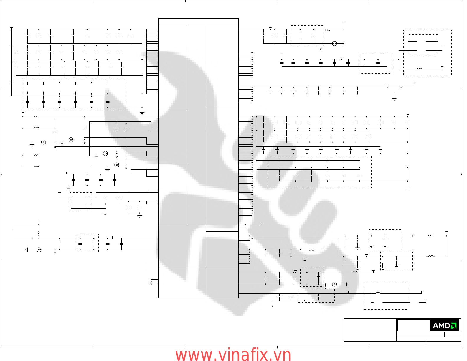
Part 3 of 7
Part 3 of 7
MEMORY INTERFACE A
MEMORY INTERFACE A
DDR1 DDR2 DDR3
DDR1 DDR2 DDR3
bidir. differential strobe
write strobe
bidir. differential strobe
write strobe
Not used
Not used
For DDR2
For DDR2
read strobe
read strobe
bidir. strobe
bidir. strobe
MAA_0
MAA_1
MAA_2
MAA_3
MAA_4
MAA_5
MAA_6
MAA_7
MAA_8
MAA_9
MAA_10
MAA_11
MAA_A12
MAA_BA0
MAA_BA1
MAA_BA2
DQMAB_0
DQMAB_1
DQMAB_2
DQMAB_3
DQMAB_4
DQMAB_5
DQMAB_6
DQMAB_7
QSA_0
QSA_1
QSA_2
QSA_3
QSA_4
QSA_5
QSA_6
QSA_7
QSA_0B
QSA_1B
QSA_2B
QSA_3B
QSA_4B
QSA_5B
QSA_6B
QSA_7B
ODTA0
ODTA1
CLKA0
CLKA0B
CKEA0
RASA0B
CASA0B
WEA0B
CSA0B_0
CSA0B_1
CLKA1
CLKA1B
CKEA1
RASA1B
CASA1B
WEA1B
CSA1B_0
CSA1B_1
DQB_[63..0](9)
MAA_0
C27
MAA_1
B28
MAA_2
B27
MAA_3
G26
MAA_4
F27
MAA_5
E27
MAA_6
D27
MAA_7
J27
MAA_8
E29
MAA_9
C30
MAA_10
E26
MAA_11
A27
MAA_12
G27
MAA_BA0
C28
MAA_BA1
B29
MAA_BA2
D26
DQMAb_0
M29
DQMAb_1
K33
DQMAb_2
G30
DQMAb_3
E33
DQMAb_4
C22
DQMAb_5
H21
DQMAb_6
C17
DQMAb_7
G17
QSA_0
M30
QSA_1
K34
QSA_2
G31
QSA_3
E34
QSA_4
B22
QSA_5
F21
QSA_6
B17
QSA_7
D17
M31
K35
G32
E35
A22
E21
A17
E17
C31
ODTA0 (8)
C25
A33
CLKA0 (8)
B33
CLKA0b (8)
B31
CKEA0 (8)
A31
RASA0b (8)
C32
CASA0b (8)
C29
WEA0b (8)
A30
CSA0b_0 (8)
B30
A26
CLKA1 (8)
B26
CLKA1b (8)
F24
CKEA1 (8)
D24
RASA1b (8)
H26
CASA1b (8)
D22
WEA1b (8)
G24
CSA1b_0 (8)
H24
MAA_[12..0] (8)
MAA_BA[2..0] (8)
DQMAb_[7..0] (8)
QSA_[7..0] (8)
+MVDD
+MVDD
R391
R391
100R
100R
1%
R392
R392
100R
100R
1%
R393
R393
100R
100R
1%
R394
R394
100R
100R
1%
C391
C391
100nF
100nF
C393
C393
100nF
100nF
C392
C392
10nF
10nF
C394
C394
10nF
10nF
MVREFD_1MVREFD_0
MVREFS_1
R296
R296
4.7K
4.7K
DQB_0
DQB_1
DQB_2
DQB_3
DQB_4
DQB_5
DQB_6
DQB_7
DQB_8
DQB_9
DQB_10
DQB_11
DQB_12
DQB_13
DQB_14
DQB_15
DQB_16
DQB_17
DQB_18
DQB_19
DQB_20
DQB_21
DQB_22
DQB_23
DQB_24
DQB_25
DQB_26
DQB_27
DQB_28
DQB_29
DQB_30
DQB_31
DQB_32
DQB_33
DQB_34
DQB_35
DQB_36
DQB_37
DQB_38
DQB_39
DQB_40
DQB_41
DQB_42
DQB_43
DQB_44
DQB_45
DQB_46
DQB_47
DQB_48
DQB_49
DQB_50
DQB_51
DQB_52
DQB_53
DQB_54
DQB_55
DQB_56
DQB_57
DQB_58
DQB_59
DQB_60
DQB_61
DQB_62
DQB_63
R297
R297
4.7K
4.7K
R298
R298
243R
243R
U1D
U1D
H15
G14
E14
D14
H12
G12
F12
D10
B13
C12
B12
B11
C9
B9
A9
B8
J10
H10
F10
D9
G7
G6
F6
D6
C8
C7
B7
A7
B5
A5
C4
B4
M3
M2
N2
N1
R3
R2
T3
T2
M8
M7
P5
P4
R9
R8
R6
U4
U3
U2
U1
V2
Y3
Y2
AA2
AA1
U9
U7
U6
V4
W9
W7
W6
W4
B14
A13
AA4
AA8
AA7
AA5
RV635 PRO A11
RV635 PRO A11
DQB_0
DQB_1
DQB_2
DQB_3
DQB_4
DQB_5
DQB_6
DQB_7
DQB_8
DQB_9
DQB_10
DQB_11
DQB_12
DQB_13
DQB_14
DQB_15
DQB_16
DQB_17
DQB_18
DQB_19
DQB_20
DQB_21
DQB_22
DQB_23
DQB_24
DQB_25
DQB_26
DQB_27
DQB_28
DQB_29
DQB_30
DQB_31
DQB_32
DQB_33
DQB_34
DQB_35
DQB_36
DQB_37
DQB_38
DQB_39
DQB_40
DQB_41
DQB_42
DQB_43
DQB_44
DQB_45
DQB_46
DQB_47
DQB_48
DQB_49
DQB_50
DQB_51
DQB_52
DQB_53
DQB_54
DQB_55
DQB_56
DQB_57
DQB_58
DQB_59
DQB_60
DQB_61
DQB_62
DQB_63
MVREFDB
MVREFSB
DRAM_RST
TEST_MCLK
TEST_YCLK
MEMTEST
Part 4 of 7
Part 4 of 7
MEMORY INTERFACE B
MEMORY INTERFACE B
DDR1 DDR2 DDR3
DDR1 DDR2 DDR3
write strobe
write strobe
Not used
Not used
bidir. differential strobe
bidir. differential strobe
For DDR2
For DDR2
bidir. strobe
read strobe
bidir. strobe
read strobe
MAB_0
MAB_1
MAB_2
MAB_3
MAB_4
MAB_5
MAB_6
MAB_7
MAB_8
MAB_9
MAB_10
MAB_11
MAB_A12
MAB_BA0
MAB_BA1
MAB_BA2
DQMBB_0
DQMBB_1
DQMBB_2
DQMBB_3
DQMBB_4
DQMBB_5
DQMBB_6
DQMBB_7
QSB_0
QSB_1
QSB_2
QSB_3
QSB_4
QSB_5
QSB_6
QSB_7
QSB_0B
QSB_1B
QSB_2B
QSB_3B
QSB_4B
QSB_5B
QSB_6B
QSB_7B
ODTB0
ODTB1
CLKB0
CLKB0B
CKEB0
RASB0B
CASB0B
WEB0B
CSB0B_0
CSB0B_1
CLKB1
CLKB1B
CKEB1
RASB1B
CASB1B
WEB1B
CSB1B_0
CSB1B_1
MAB_0
H2
MAB_1
H3
MAB_2
J3
MAB_3
J5
MAB_4
J4
MAB_5
J6
MAB_6
G5
MAB_7
J9
MAB_8
F3
MAB_9
F4
MAB_10
J1
MAB_11
J2
MAB_12
J7
MAB_BA0
G2
MAB_BA1
G3
MAB_BA2
F1
DQMBb_0
D12
DQMBb_1
C10
DQMBb_2
E7
DQMBb_3
C6
DQMBb_4
P3
DQMBb_5
R4
DQMBb_6
W3
DQMBb_7
V8
QSB_0
J14
QSB_1
B10
QSB_2
F9
QSB_3
B6
QSB_4
P2
QSB_5
P8
QSB_6
W2
QSB_7
V6
H14
A10
E9
A6
P1
P7
W1
V5
D2
ODTB0 (9)
K5
A3
CLKB0 (9)
B3
CLKB0b (9)
E3
CKEB0 (9)
D3
RASB0b (9)
C1
CASB0b (9)
F2
WEB0b (9)
E1
CSB0b_0 (9)
E2
K1
CLKB1 (9)
K2
CLKB1b (9)
K8
CKEB1 (9)
K7
RASB1b (9)
K4
CASB1b (9)
M6
WEB1b (9)
L3
CSB1b_0 (9)
M4
MAB_[12..0] (9)
MAB_BA[2..0] (9)
DQMBb_[7..0] (9)
QSB_[7..0] (9)
D D
C C
B B
A A
CONFIDENTIAL & PROPRIETARY TO ADVANCED MICRO DEVICES INC.
CONFIDENTIAL & PROPRIETARY TO ADVANCED MICRO DEVICES INC.
CONFIDENTIAL & PROPRIETARY TO ADVANCED MICRO DEVICES INC.
© 2007 Advanced Micro Devices
© 2007 Advanced Micro Devices
© 2007 Advanced Micro Devices
This AMD Board schematic and design is the exclusive property of AMD,
This AMD Board schematic and design is the exclusive property of AMD,
This AMD Board schematic and design is the exclusive property of AMD,
and is provided only to entities under a non-disclosure agreement
and is provided only to entities under a non-disclosure agreement
and is provided only to entities under a non-disclosure agreement
with AMD for evaluation purposes. Further distribution or disclosure
with AMD for evaluation purposes. Further distribution or disclosure
with AMD for evaluation purposes. Further distribution or disclosure
is strictly prohibited. Use of this schematic and design for any purpose
is strictly prohibited. Use of this schematic and design for any purpose
is strictly prohibited. Use of this schematic and design for any purpose
other than evaluation requires a Board Technology License Agreement
other than evaluation requires a Board Technology License Agreement
other than evaluation requires a Board Technology License Agreement
with AMD. AMD makes no representations or warranties of any kind
with AMD. AMD makes no representations or warranties of any kind
with AMD. AMD makes no representations or warranties of any kind
regarding this schematic and design, including, not limited to,
regarding this schematic and design, including, not limited to,
regarding this schematic and design, including, not limited to,
any implied warranty of merchantibility or fitness for a particular
any implied warranty of merchantibility or fitness for a particular
any implied warranty of merchantibility or fitness for a particular
purpose, and disclaims responsibility forany consequences resulting
purpose, and disclaims responsibility forany consequences resulting
purpose, and disclaims responsibility forany consequences resulting
from use of the information included herein.
from use of the information included herein.
from use of the information included herein.
Title
Title
Title
RV635 DDR2 - ASIC Memory Interface (Channel A & B)
RV635 DDR2 - ASIC Memory Interface (Channel A & B)
5
4
3
2
RV635 DDR2 - ASIC Memory Interface (Channel A & B)
Advanced Micro Devices Inc.
Advanced Micro Devices Inc.
Advanced Micro Devices Inc.
1 Commerce Valley Drive East
1 Commerce Valley Drive East
1 Commerce Valley Drive East
Markham, Ontario
Markham, Ontario
Markham, Ontario
Thursday, January 24, 2008
Thursday, January 24, 2008
Thursday, January 24, 2008
Sheet
Sheet
Sheet
of
520
of
520
of
520
1
Doc No.
Doc No.
Doc No.
RevDate:
RevDate:
RevDate:
13
13
13
102-B38101-00
102-B38101-00
102-B38101-00
www.vinafix.vn
Page 6
5
D D
C C
B B
A A
5
4
U1F
U1F
P33
PCIE_VSS_1
V29
PCIE_VSS_2
AB32
PCIE_VSS_3
AG29
PCIE_VSS_4
AJ29
PCIE_VSS_5
AJ32
PCIE_VSS_6
AK32
PCIE_VSS_7
AL34
PCIE_VSS_8
AL35
PCIE_VSS_9
P34
PCIE_VSS_10
P35
PCIE_VSS_11
R27
PCIE_VSS_12
R28
PCIE_VSS_13
R29
PCIE_VSS_14
R32
PCIE_VSS_15
R33
PCIE_VSS_16
T33
PCIE_VSS_17
U29
PCIE_VSS_18
U32
PCIE_VSS_19
V32
PCIE_VSS_20
V34
PCIE_VSS_21
V35
PCIE_VSS_22
W29
PCIE_VSS_23
W32
PCIE_VSS_24
W33
PCIE_VSS_25
Y33
PCIE_VSS_26
AA29
PCIE_VSS_27
AA32
PCIE_VSS_28
AB29
PCIE_VSS_29
AB34
PCIE_VSS_30
AB35
PCIE_VSS_31
AC33
PCIE_VSS_43
AD29
PCIE_VSS_32
AD32
PCIE_VSS_33
AD33
PCIE_VSS_34
AF29
PCIE_VSS_35
AF32
PCIE_VSS_36
AF34
PCIE_VSS_37
AF35
PCIE_VSS_38
AG27
PCIE_VSS_39
AG32
PCIE_VSS_40
AG33
PCIE_VSS_41
AH33
PCIE_VSS_42
A2
VSS_1
P15
VSS_2
R14
VSS_3
V1
VSS_4
W8
VSS_5
AA19
VSS_6
AC17
VSS_7
AF19
VSS_8
AK3
VSS_9
A4
VSS_10
C18
VSS_11
E22
VSS_12
G4
VSS_13
J18
VSS_14
K17
VSS_15
M28
VSS_16
P6
VSS_17
P9
VSS_18
P13
VSS_19
P18
VSS_20
P21
VSS_21
P23
VSS_22
P26
VSS_23
P29
VSS_24
P30
VSS_25
R1
VSS_26
R5
VSS_27
R7
VSS_28
R10
VSS_29
R17
VSS_30
R19
VSS_31
R22
VSS_32
U5
VSS_33
U8
VSS_34
U10
VSS_35
U15
VSS_36
U18
VSS_37
U21
VSS_38
U23
VSS_39
V3
VSS_40
V7
VSS_41
V9
VSS_42
V10
VSS_43
V11
VSS_44
V14
VSS_45
V17
VSS_46
V19
VSS_47
V22
VSS_48
W5
VSS_49
W10
VSS_50
W15
VSS_51
W18
VSS_52
W21
VSS_53
W23
VSS_54
AA3
VSS_55
AA6
VSS_56
AA10
VSS_57
AA14
VSS_58
AA17
VSS_59
AA22
VSS_60
AB5
VSS_61
AB8
VSS_62
AB10
VSS_63
AB13
VSS_64
AB15
VSS_65
AB18
VSS_66
AB21
VSS_67
AB23
VSS_68
AC14
VSS_69
AC19
VSS_70
AC22
VSS_71
AD6
VSS_72
AD24
VSS_73
AF6
VSS_74
AF9
VSS_75
AF14
VSS_76
AF15
VSS_77
AF17
VSS_78
AF18
VSS_79
AF21
VSS_80
AF22
VSS_81
AF24
VSS_82
AG10
VSS_83
AG12
VSS_84
AH21
VSS_85
RV635 PRO A11
RV635 PRO A11
4
Part 6 of 7
Part 6 of 7
PCI-Express GND
PCI-Express GND
CORE GND
CORE GND
3
VSS_100
VSS_101
VSS_102
VSS_103
VSS_104
VSS_105
VSS_106
VSS_107
VSS_108
VSS_109
VSS_110
VSS_111
VSS_112
VSS_113
VSS_114
VSS_115
VSS_116
VSS_117
VSS_118
VSS_119
VSS_120
VSS_121
VSS_122
VSS_123
VSS_124
VSS_125
VSS_126
VSS_127
VSS_128
VSS_129
VSS_130
VSS_131
VSS_132
VSS_133
VSS_134
VSS_135
VSS_136
VSS_137
VSS_138
VSS_139
VSS_140
VSS_141
VSS_142
VSS_143
VSS_144
VSS_145
VSS_146
VSS_147
VSS_148
VSS_149
VSS_150
VSS_151
VSS_152
VSS_153
VSS_154
VSS_155
VSS_156
VSS_157
VSS_158
VSS_159
VSS_160
VSS_161
VSS_162
VSS_163
VSS_164
VSS_165
VSS_166
3
VSS_86
VSS_87
VSS_88
VSS_89
VSS_90
VSS_91
VSS_92
VSS_93
VSS_94
VSS_95
VSS_96
VSS_97
VSS_98
VSS_99
BBN_1
BBN_2
AJ14
AJ17
AJ18
AJ19
AK9
AK10
AK12
AK15
AK30
AM1
AN3
AN6
AN32
AR8
A11
A18
A21
A29
A34
C3
C5
C11
C13
C14
C23
C26
C33
D4
D7
D29
D33
E10
E12
E19
E24
F7
F14
F15
F17
F26
F30
F33
F35
G1
G9
G10
G18
G21
G22
G29
H17
H19
J12
J15
J21
J24
J26
J32
J35
K3
K6
K9
K14
K15
K18
K19
K21
K22
K28
K30
L33
M5
M9
M26
M32
N3
N14
N17
N19
N22
N33
W13
AA13
2
CONFIDENTIAL & PROPRIETARY TO ADVANCED MICRO DEVICES INC.
CONFIDENTIAL & PROPRIETARY TO ADVANCED MICRO DEVICES INC.
CONFIDENTIAL & PROPRIETARY TO ADVANCED MICRO DEVICES INC.
© 2007 Advanced Micro Devices
© 2007 Advanced Micro Devices
© 2007 Advanced Micro Devices
This AMD Board schematic and design is the exclusive property of AMD,
This AMD Board schematic and design is the exclusive property of AMD,
This AMD Board schematic and design is the exclusive property of AMD,
and is provided only to entities under a non-disclosure agreement
and is provided only to entities under a non-disclosure agreement
and is provided only to entities under a non-disclosure agreement
with AMD for evaluation purposes. Further distribution or disclosure
with AMD for evaluation purposes. Further distribution or disclosure
with AMD for evaluation purposes. Further distribution or disclosure
is strictly prohibited. Use of this schematic and design for any purpose
is strictly prohibited. Use of this schematic and design for any purpose
is strictly prohibited. Use of this schematic and design for any purpose
other than evaluation requires a Board Technology License Agreement
other than evaluation requires a Board Technology License Agreement
other than evaluation requires a Board Technology License Agreement
with AMD. AMD makes no representations or warranties of any kind
with AMD. AMD makes no representations or warranties of any kind
with AMD. AMD makes no representations or warranties of any kind
regarding this schematic and design, including, not limited to,
regarding this schematic and design, including, not limited to,
regarding this schematic and design, including, not limited to,
any implied warranty of merchantibility or fitness for a particular
any implied warranty of merchantibility or fitness for a particular
any implied warranty of merchantibility or fitness for a particular
purpose, and disclaims responsibility forany consequences resulting
purpose, and disclaims responsibility forany consequences resulting
purpose, and disclaims responsibility forany consequences resulting
from use of the information included herein.
from use of the information included herein.
from use of the information included herein.
Title
Title
Title
RV635 DDR2 - ASIC Grounds
RV635 DDR2 - ASIC Grounds
2
RV635 DDR2 - ASIC Grounds
Sheet
Sheet
Sheet
1
Advanced Micro Devices Inc.
Advanced Micro Devices Inc.
Advanced Micro Devices Inc.
1 Commerce Valley Drive East
1 Commerce Valley Drive East
1 Commerce Valley Drive East
Markham, Ontario
Markham, Ontario
Markham, Ontario
Thursday, January 24, 2008
Thursday, January 24, 2008
Thursday, January 24, 2008
of
620
of
620
of
620
1
Doc No.
Doc No.
Doc No.
RevDate:
RevDate:
RevDate:
13
13
13
102-B38101-00
102-B38101-00
102-B38101-00
www.vinafix.vn
Page 7
5
VID_0
VID_1
VID_2
VID_3
VID_4
VID_5
VID_6
VID_7
D D
DVOCLK
TP84 35milTP84 35mil
DVPCNTL_0
TP85 35milTP85 35mil
DVPCNTL_1
TP86 35milTP86 35mil
DVPCNTL_2
TP87 35milTP87 35mil
DVP_MVP_CNTL_0
TP88 35milTP88 35mil
DVP_MVP_CNTL_1
CrossFire
DVP_MVP_CNTL_0 : DE for bits D[12..23]
DVP_MVP_CNTL_1 : CLK for bits D[12..23]
C C
B B
TP89 35milTP89 35mil
TP60 35milTP60 35mil
TP61 35milTP61 35mil
TP62 35milTP62 35mil
TP63 35milTP63 35mil
TP64 35milTP64 35mil
TP65 35milTP65 35mil
TP66 35milTP66 35mil
TP67 35milTP67 35mil
TP68 35milTP68 35mil
TP69 35milTP69 35mil
TP70 35milTP70 35mil
TP71 35milTP71 35mil
TP72 35milTP72 35mil
TP73 35milTP73 35mil
TP74 35milTP74 35mil
TP75 35milTP75 35mil
TP76 35milTP76 35mil
TP77 35milTP77 35mil
TP78 35milTP78 35mil
TP79 35milTP79 35mil
TP80 35milTP80 35mil
TP81 35milTP81 35mil
TP82 35milTP82 35mil
TP83 35milTP83 35mil
DVPDATA_0
DVPDATA_1
DVPDATA_2
DVPDATA_3
DVPDATA_4
DVPDATA_5
DVPDATA_6
DVPDATA_7
DVPDATA_8
DVPDATA_9
DVPDATA_10
DVPDATA_11
DVPDATA_12
DVPDATA_13
DVPDATA_14
DVPDATA_15
DVPDATA_16
DVPDATA_17
DVPDATA_18
DVPDATA_19
DVPDATA_20
DVPDATA_21
DVPDATA_22
DVPDATA_23
AM12
AL12
AJ12
AH12
AM10
AL10
AJ10
AH10
AL7
AM9
AL9
AJ9
AK7
AH1
AG1
AH3
AH2
AN8
AP8
AJ3
AJ2
AJ1
AK2
AK1
AL3
AL2
AL1
AM3
AM2
AN2
AP3
AR3
AN4
AR4
AP4
AN5
AR5
AP5
AP6
AR6
AN7
AP7
AR7
U1G
U1G
VIP_0
VIP_1
VIP_2
VIP_3
VIP_4
VIP_5
VIP_6
VIP_7
VPCLK0
VHAD_0
VHAD_1
VPHCTL
VIPCLK
DVPCLK
DVPCNTL_0
DVPCNTL_1
DVPCNTL_2
DVPCNTL_MVP_0
DVPCNTL_MVP_1
DVPDATA_0
DVPDATA_1
DVPDATA_2
DVPDATA_3
DVPDATA_4
DVPDATA_5
DVPDATA_6
DVPDATA_7
DVPDATA_8
DVPDATA_9
DVPDATA_10
DVPDATA_11
DVPDATA_12
DVPDATA_13
DVPDATA_14
DVPDATA_15
DVPDATA_16
DVPDATA_17
DVPDATA_18
DVPDATA_19
DVPDATA_20
DVPDATA_21
DVPDATA_22
DVPDATA_23
RV635 PRO A11
RV635 PRO A11
VIP
VIP
Capture
Capture
VIP
VIP
Host
Host
PART 7 OF 7
PART 7 OF 7
General
General
Purpose
Purpose
I/O
I/O
GPIO_15_PWRCNTL_0
GPIO_17_THERMAL_INT
GPIO_20_PWRCNTL_1
GPIO_23_CLKREQB
RESERVED
RESERVED
No Connect
No Connect
GPIO_0
GPIO_1
GPIO_2
GPIO_3
GPIO_4
GPIO_5
GPIO_6
GPIO_7_BLON
GPIO_8_ROMSO
GPIO_9_ROMSI
GPIO_10_ROMSCK
GPIO_11
GPIO_12
GPIO_13
GPIO_14_HPD2
GPIO_16_SSIN
GPIO_18_HPD3
GPIO_19_CTF
GPIO_21_BB_EN
GPIO_22_ROMCSB
GPIO_24_TRST
GPIO_25_TDI
GPIO_26_TCK
GPIO_27_TMS
GPIO_28_TDO
GEN_A
GEN_B
GEN_C
GEN_D_HPD4
GEN_E
GEN_F
GEN_G
DVALID
PSYNC
RSVD_1
RSVD_2
RSVD_3
RSVD_4
RSVD_5
RSVD_6
RSVD_7
RSVD_8
NC_1
NC_2
NC_3
NC_DRM_0
NC_DRM_1
NC_FAN_TACH
NC_AC_BATT
NC_SMBCLK
NC_SMBDATA
4
GPIO_0
AG2
GPIO_1
AF2
GPIO_2
AF1
AE3
AE2
AE1
AD3
AD2
AD1
AD5
AD4
AC3
AC2
AC1
AB3
AB2
AB1
AF5
AF4
AG4
AG3
AD9
AD8
AD7
AB4
AB6
AB7
AB9
AA9
AF8
AF7
AG5
AP9
AR9
AP13
AR13
AJ7
AM7
AG24
AH24
AK24
AK26
AL24
AL26
AG7
AJ6
AG18
AH18
AM34
AF3
AG9
AK14
AK29
AK34
AK35
JTAG_TDI
JTAG_TCK
JTAG_TMS
JTAG_TDO
GND_PCIE_PVSS
GPIO_3
GPIO_4
GPIO_5
GPIO_6
GPIO_7 GPIO_3
GPIO_8
GPIO_9
GPIO_10
GPIO_11
GPIO_12
GPIO_13
HPD2
PWRCNTL_0
GPIO_16
ThermINT
GPIO_18_HPD3
CTF
PWRCNTL_1
GPIO21_BB_EN
GPIO_22
GENERICA
GENERICB
GENERICC
GEN_D_HPD4
DVALID
PSYNC
CrossFire
FLOW_CONTROL_1 - Lower Cable
FLOW_CONTROL_2 - Upper Cable
SWAP_LOCK_1 - Lower Cable
SWAP_LOCK_2 - Upper Cable
HPD2 (15)
PWRCNTL_0 (13)
ThermINT (18)
GPIO_18_HPD3 (17)
CTF (18)
PCIE_CLK_REQb
JTAG_MODE
TP52TP52
TP53TP53
TP54TP54
TP55TP55
DNI
+3.3V
SMBCLK (1)
SMBDATA (1)
PWRCNTL_1 (13)
MR51KMR5
1K
3
BUO
TP51TP51
GEN_D_HPD4_TDO (1)
+3.3V
DNI
DNI
MR55 10KMR55 10K
TP50TP50
DNI
MR78 10KMR78 10K
DNI
MR87 10KMR87 10K
+3.3V
DNI
DNI
DNI
DNI
NTSC
DNI
DNI
DNI
DNI
DNI
DNI
DNI
DNI
BUO
DNI
DNI
DNI
DNI
DNI
DNI
2
R50 10KR50 10K
R51 10KR51 10K
R57 10KR57 10K
R63 10KR63 10K
R61 10KR61 10K
R73 10KR73 10K
PIN BASED STRAPS
GPIO_0
GPIO_1
GPIO_1
GPIO_2
GPIO_2
GPIO_3
GPIO_5
GPIO_7GPIO_7
GPIO_8_R
GPIO_9_R
CONFIG[3]
GPIO_13
GPIO_13
CONFIG[2]
GPIO_12
GPIO_12
CONFIG[1]
GPIO_11
GPIO_11
CONFIG[0]
GENERICC
GENERICB
VSYNC_DAC1
VSYNC_DAC1
HSYNC_DAC1
PSYNC
PSYNC
GPIO21_BB_EN
GPIO21_BB_EN
VID_0
VID_0
VID_1
VID_1
VID_2
VID_2
VID_3
VID_3
VID_4
VID_4
VID_5
VID_5
VID_6
VID_6
VID_7
VID_7
VSYNC_DAC2
VSYNC_DAC2
VSYNC_DAC1 (3,15)
HSYNC_DAC1 (3,15)
VSYNC_DAC2 (3,16)
GPIO_18_HPD3
HSYNC_DAC2
HSYNC_DAC2
HSYNC_DAC2 (3,16)
DVALIDDVALID
GPIO_16
GPIO_4
GPIO_6
1
GPIO(0) - TX_PWRS_ENB (Transmitter Power Savings Enable)
0: 50% Tx output swing for mobile mode
1: full Tx output swing (Default setting for Desktop)
GPIO(1) - TX_DEEMPH_EN (Transmitter De-emphasis Enable)
0: Tx de-emphasis disabled for mobile mode
1: Tx de-emphasis enabled (Default setting for Desktop)
AMD Internal Use Only - Reserved (Default: 00)
DEBUG_ACCESS
AMD Internal Use Only - Reserved (Default: 0)
AMD Internal Use Only - Reserved (Default: G1=0, G2=1)
AMD Internal Use Only - Reserved (Default: 0)
TV OUT STANDARD (Jumper position overwrite resistor settings)
0 - PAL TVO (Jumper is closed)
1 - NTSC TVO (Jumper is open)
AMD Internal Use Only - Reserved (Default: 0)
GPIO(9,13:11) - CONFIG[3..0]
0010 - 512Kbit AT25F512A (Atmel)
0011 - 1Mbit AT25F1024A (Atmel)
0100 - 512Kbit M25P05A (ST)
0101 - 1Mbit M25P10A (ST)
0101 - 2Mbit M25P20 (ST)
0100 - 512Kbit Pm25LV512 (Chingis)
0101 - 1Mbit Pm25LV010 (Chingis)
AMD Internal Use Only - Reserved (Default: 0)
VIP_DEVICE_STRAP_EN
0: Slave VIP host port devices present (use if Theater is populated)
1: No slave VIP host port devices reporting presence during reset (use for
configurations without video-in)
AMD Internal Use Only - Reserved (HDMI_EN =1 )
VGA DISABLE : 1 for disable (set to 0 for normal operation)
AMD Internal Use Only - Reserved (Default: 0)
AMD Internal Use Only - Reserved (Default: 0)
MSI_DIS (Default: 0)
AMD Internal Use Only - Reserved (Default: 0)
BIF_AUDIO_EN
0 - Disable HD Audio 1- Enable HD Audio (Default 1 for RV635)
AMD Internal Use Only - Reserved (Default: 0)
64BAR_EN_A (Default: 0)
AMD Internal Use Only - Reserved (Default: 0)
AMD Internal Use Only - Reserved (Default: 0)
MEMORY CONFIG
[V2SYNC: GPIO_18_HDP3]
Quimonda [0:0]
Hynix [0:1]
Samsung [1:0]
AMD Internal Use Only - Reserved
BIF_CLK_PM_EN
0 - Disable CLKREQ# power management capability
1 - Enable CLKREQ# power management capability
ATI Board Feature I
Default: 0
ATI PCIE FEATURE I
ATI PCIE FEATURE II
CrossFire Card-Edge
GPIO_8_R
GPIO_9_R
GPIO_10_R
GPIO_22_R
+3.3V
+3.3V
R46
R46
10K
10K
U2
U2
5
6
1
7
3
8
M25P05-AVNM6P
M25P05-AVNM6P
D
C
S
HOLD
W
VCC
2
Q
4
VSS
Advanced Micro Devices Inc.
Advanced Micro Devices Inc.
Advanced Micro Devices Inc.
1 Commerce Valley Drive East
1 Commerce Valley Drive East
1 Commerce Valley Drive East
Markham, Ontario
Markham, Ontario
Markham, Ontario
Thursday, January 24, 2008
Thursday, January 24, 2008
Thursday, January 24, 2008
Sheet
Sheet
Sheet
of
720
of
720
of
720
1
BIOS1
BIOS1
VIDEO BIOS
FIRMWARE
BIOS
BIOS
113-B381XX-XXX
113-B381XX-XXX
Doc No.
Doc No.
Doc No.
RevDate:
RevDate:
RevDate:
13
13
13
102-B38101-00
102-B38101-00
102-B38101-00
Lower Cable Card Edge
J8002J8002
1
DVOCLK
DVPCNTL_2
DVPDATA_1
DVPDATA_3
DVPDATA_5
DVPDATA_7
DVPDATA_9
DVPDATA_11
DVPCNTL_1
A A
GPIO_3
3
5
7
9
11
13
15
17
19
21
23
25
27
29 30
31
33
35
37
39
2
4
6
8
DVPDATA_0
10
12
DVPDATA_2
14
16
DVPDATA_4
18
20
DVPDATA_6
22
24
DVPDATA_8
26
28
DVPDATA_10
32
DVPCNTL_0
34
36
GPIO_5
38
40
Bundle A
5
Upper Cable Card Edge
J8001J8001
1
DVP_MVP_CNTL_1
DVP_MVP_CNTL_0
DVPDATA_13
DVPDATA_15
DVPDATA_17
DVPDATA_19
DVPDATA_21
DVPDATA_23
GENERICB_R
GPIO_4
3
5
7
9
11
13
15
17
19
21
23
25
27
29 30
31
33
35
37
39
2
4
6
8
DVPDATA_12
10
12
DVPDATA_14
14
16
DVPDATA_16
18
20
DVPDATA_18
22
24
DVPDATA_20
26
28
DVPDATA_22
32
DVALID_R
34
36
GPIO_6
38
40
Bundle B (closer to the bracket)
4
Do not install for BU
DVALID
GENERICB
GENERICB: Generic I2C_SDA
DVALID: Generic I2C_SCL
Place close to ASIC
GPIO_8
R37 33RR37 33R
GPIO_9
R47 33RR47 33R
GPIO_10
R48 33RR48 33R
GPIO_22
R49 33RR49 33R
+3.3V
R45
R45
10K
10K
CONFIDENTIAL & PROPRIETARY TO ADVANCED MICRO DEVICES INC.
CONFIDENTIAL & PROPRIETARY TO ADVANCED MICRO DEVICES INC.
CONFIDENTIAL & PROPRIETARY TO ADVANCED MICRO DEVICES INC.
© 2007 Advanced Micro Devices
© 2007 Advanced Micro Devices
© 2007 Advanced Micro Devices
This AMD Board schematic and design is the exclusive property of AMD,
This AMD Board schematic and design is the exclusive property of AMD,
This AMD Board schematic and design is the exclusive property of AMD,
and is provided only to entities under a non-disclosure agreement
and is provided only to entities under a non-disclosure agreement
and is provided only to entities under a non-disclosure agreement
with AMD for evaluation purposes. Further distribution or disclosure
with AMD for evaluation purposes. Further distribution or disclosure
with AMD for evaluation purposes. Further distribution or disclosure
is strictly prohibited. Use of this schematic and design for any purpose
is strictly prohibited. Use of this schematic and design for any purpose
is strictly prohibited. Use of this schematic and design for any purpose
other than evaluation requires a Board Technology License Agreement
other than evaluation requires a Board Technology License Agreement
other than evaluation requires a Board Technology License Agreement
with AMD. AMD makes no representations or warranties of any kind
with AMD. AMD makes no representations or warranties of any kind
with AMD. AMD makes no representations or warranties of any kind
regarding this schematic and design, including, not limited to,
regarding this schematic and design, including, not limited to,
regarding this schematic and design, including, not limited to,
any implied warranty of merchantibility or fitness for a particular
any implied warranty of merchantibility or fitness for a particular
any implied warranty of merchantibility or fitness for a particular
purpose, and disclaims responsibility forany consequences resulting
purpose, and disclaims responsibility forany consequences resulting
purpose, and disclaims responsibility forany consequences resulting
from use of the information included herein.
from use of the information included herein.
from use of the information included herein.
Title
Title
Title
RV635 DDR2 - ASIC DVO & GPIOs
RV635 DDR2 - ASIC DVO & GPIOs
3
2
RV635 DDR2 - ASIC DVO & GPIOs
www.vinafix.vn
Page 8

5
4
3
2
1
CHANNEL A: 128MB/256MB DDR2
DQA_[63..0](5)
D D
C C
MAA_BA[2..0](5)
MAA_[12..0](5)
+MVDD +MVDD +MVDD
R201
R201
4.99K
4.99K
VREF_U201
C202
C202
R202
R202
100nF_6.3V
100nF_6.3V
4.99K
4.99K
MAA_BA0
MAA_BA1
MAA_BA2 MAA_BA2 MAA_BA2 MAA_BA2
MAA_12
MAA_11
MAA_10
MAA_9
MAA_8
MAA_7
MAA_6
MAA_5
MAA_4
MAA_3
MAA_2
MAA_1
MAA_0
CLKA0b(5)
CLKA0(5)
CKEA0(5)
CSA0b_0(5)
WEA0b(5)
RASA0b(5)
CASA0b(5)
DQMAb_3
DQMAb_0
ODTA0(5)
QSA_3
VREF_A0
QSA_0
VREF_A0
U201
U201
L2
BA0
L3
BA1
L1
BA2
R2
A12
P7
A11
M2
A10/AP
P3
A9
P8
A8
P2
A7
N7
A6
N3
A5
N8
A4
N2
A3
M7
A2
M3
A1
M8
A0
K8
CK
J8
CK
K2
CKE
L8
CS
WEK3VDDQ10
K7
RAS
L7
CAS
F3
LDM
B3
UDM
K9
ODT
F7
LDQS
E8
LDQS
B7
UDQS
A8
UDQS
J2
VREF
A2
NC#A2
E2
NC#E2
R3
NC#R3
R7
NC#R7
R8
NC#R8
23BC1147SP02
23BC1147SP02
DQ15
DQ14
DQ13
DQ12
DQ11
DQ10
VDDQ1
VDDQ2
VDDQ3
VDDQ4
VDDQ5
VDDQ6
VDDQ7
VDDQ8
VDDQ9
VDD1
VDD2
VDD3
VDD4
VDD5
VDDL
VSSDL
VSSQ1
VSSQ2
VSSQ3
VSSQ4
VSSQ5
VSSQ6
VSSQ7
VSSQ8
VSSQ9
VSSQ10
VSS1
VSS2
VSS3
VSS4
VSS5
U202
DQA_3
B9
DQA_5
B1
DQA_0
D9
DQA_4
D1
DQA_7
D3
DQA_1
D7
DQA_6
C2
DQ9
DQA_2
C8
DQ8
DQA_27
F9
DQ7
DQA_28
F1
DQ6
DQA_26
H9
DQ5
DQA_31
H1
DQ4
DQA_30
H3
DQ3
DQA_24
H7
DQ2
DQA_29
G2
DQ1
DQA_25
G8
DQ0
A9
C1
C3
C7
C9
E9
G1
G3
G7
G9
A1
E1
J9
M9
R1
J1
J7
A7
B2
B8
D2
D8
E7
F2
F8
H2
H8
A3
E3
J3
N1
P9
B201
B201
220R_200mA
220R_200mA
C200
C200
100nF_6.3V
100nF_6.3V
R203
R203
4.99K
4.99K
R204
R204
4.99K
4.99K
+MVDD
+MVDD
C201
C201
1uF_6.3V
1uF_6.3V
VREF_U202
C205
C205
100nF_6.3V
100nF_6.3V
MAA_BA0
MAA_BA1
MAA_12
MAA_11
MAA_10
MAA_9
MAA_8
MAA_7
MAA_6
MAA_5
MAA_4
MAA_3
MAA_2
MAA_1
MAA_0
CLKA0b(5)
CLKA0(5)
CKEA0(5)
CSA0b_0(5)
WEA0b(5)
RASA0b(5)
CASA0b(5)
DQMAb_1
DQMAb_2
ODTA0(5) ODTA0(5)
QSA_1 QSA_5
VREF_A0
QSA_2
VREF_A0
U202
L2
BA0
L3
BA1
L1
BA2
R2
A12
P7
A11
M2
A10/AP
P3
A9
P8
A8
P2
A7
N7
A6
N3
A5
N8
A4
N2
A3
M7
A2
M3
A1
M8
A0
K8
CK
J8
CK
K2
CKE
L8
CS
WEK3VDDQ10
K7
RAS
L7
CAS
F3
LDM
B3
UDM
K9
ODT
F7
LDQS
E8
LDQS
B7
UDQS
A8
UDQS
J2
VREF
A2
NC#A2
E2
NC#E2
R3
NC#R3
R7
NC#R7
R8
NC#R8
23BC1147SP02
23BC1147SP02
DQ15
DQ14
DQ13
DQ12
DQ11
DQ10
VDDQ1
VDDQ2
VDDQ3
VDDQ4
VDDQ5
VDDQ6
VDDQ7
VDDQ8
VDDQ9
VDD1
VDD2
VDD3
VDD4
VDD5
VDDL
VSSDL
VSSQ1
VSSQ2
VSSQ3
VSSQ4
VSSQ5
VSSQ6
VSSQ7
VSSQ8
VSSQ9
VSSQ10
VSS1
VSS2
VSS3
VSS4
VSS5
DQA_18
B9
DQA_23
B1
DQA_16
D9
DQA_19
D1
DQA_22
D3
DQA_17
D7
DQA_21
C2
DQ9
DQA_20
C8
DQ8
DQA_12
F9
DQ7
DQA_11
F1
DQ6
DQA_15
H9
DQ5
DQA_9
H1
DQ4
DQA_8
H3
DQ3
DQA_14
H7
DQ2
DQA_10
G2
DQ1
DQA_13
G8
DQ0
A9
C1
C3
C7
C9
E9
G1
G3
G7
G9
A1
E1
J9
M9
R1
J1
J7
C203
C203
100nF_6.3V
100nF_6.3V
A7
B2
B8
D2
D8
E7
F2
F8
H2
H8
A3
E3
J3
N1
P9
B202
B202
220R_200mA
220R_200mA
R205
R205
4.99K
4.99K
R206
R206
4.99K
4.99K
C204
C204
1uF_6.3V
1uF_6.3V
VREF_U203
+MVDD
+MVDD
C208
C208
100nF_6.3V
100nF_6.3V
U203
MAA_BA0
MAA_BA1
MAA_12
MAA_11
MAA_10
MAA_9
MAA_8
MAA_7
MAA_6
MAA_5
MAA_4
MAA_3
MAA_2
MAA_1
MAA_0
CLKA1b(5)
CLKA1(5)
CKEA1(5)
CSA1b_0(5)
WEA1b(5)
RASA1b(5)
CASA1b(5)
DQMAb_4 DQMAb_7
VREF_A1
QSA_4
VREF_A1
U203
L2
BA0
L3
BA1
L1
BA2
R2
A12
P7
A11
M2
A10/AP
P3
A9
P8
A8
P2
A7
N7
A6
N3
A5
N8
A4
N2
A3
M7
A2
M3
A1
M8
A0
K8
CK
J8
CK
K2
CKE
L8
CS
WEK3VDDQ10
K7
RAS
L7
CAS
F3
LDM
B3
UDM
K9
ODT
F7
LDQS
E8
LDQS
B7
UDQS
A8
UDQS
J2
VREF
A2
NC#A2
E2
NC#E2
R3
NC#R3
R7
NC#R7
R8
NC#R8
23BC1147SP02
23BC1147SP02
DQ15
DQ14
DQ13
DQ12
DQ11
DQ10
VDDQ1
VDDQ2
VDDQ3
VDDQ4
VDDQ5
VDDQ6
VDDQ7
VDDQ8
VDDQ9
VDD1
VDD2
VDD3
VDD4
VDD5
VDDL
VSSDL
VSSQ1
VSSQ2
VSSQ3
VSSQ4
VSSQ5
VSSQ6
VSSQ7
VSSQ8
VSSQ9
VSSQ10
VSS1
VSS2
VSS3
VSS4
VSS5
DQA_34
B9
DQA_38
B1
DQA_33
D9
DQA_37
D1
DQA_39
D3
DQA_32
D7
DQA_36
C2
DQ9
DQA_35
C8
DQ8
DQA_43
F9
DQ7
DQA_45
F1
DQ6
DQA_41
H9
DQ5
DQA_47
H1
DQ4
DQA_46
H3
DQ3
DQA_42
H7
DQ2
DQA_44
G2
DQ1
DQA_40
G8
DQ0
A9
C1
C3
C7
C9
E9
G1
G3
G7
G9
A1
E1
J9
M9
R1
J1
J7
C206
C206
100nF_6.3V
100nF_6.3V
A7
+MVDD
B2
B8
D2
D8
E7
F2
F8
H2
H8
A3
E3
J3
N1
P9
B203
B203
220R_200mA
220R_200mA
R207
R207
4.99K
4.99K
R208
R208
4.99K
4.99K
C207
C207
1uF_6.3V
1uF_6.3V
VREF_U204
+MVDD
+MVDD
C211
C211
100nF_6.3V
100nF_6.3V
DQMAb_6DQMAb_5
QSA_6
VREF_A1
QSA_7
VREF_A1
MAA_BA0
MAA_BA1
MAA_12
MAA_11
MAA_10
MAA_9
MAA_8
MAA_7
MAA_6
MAA_5
MAA_4
MAA_3
MAA_2
MAA_1
MAA_0
CLKA1b(5)
CLKA1(5)
CKEA1(5)
CSA1b_0(5)
WEA1b(5)
RASA1b(5)
CASA1b(5)
ODTA0(5)
U204
U204
L2
BA0
L3
BA1
L1
BA2
R2
A12
P7
A11
M2
A10/AP
P3
A9
P8
A8
P2
A7
N7
A6
N3
A5
N8
A4
N2
A3
M7
A2
M3
A1
M8
A0
K8
CK
J8
CK
K2
CKE
L8
CS
WEK3VDDQ10
K7
RAS
L7
CAS
F3
LDM
B3
UDM
K9
ODT
F7
LDQS
E8
LDQS
B7
UDQS
A8
UDQS
J2
VREF
A2
NC#A2
E2
NC#E2
R3
NC#R3
R7
NC#R7
R8
NC#R8
23BC1147SP02
23BC1147SP02
DQ15
DQ14
DQ13
DQ12
DQ11
DQ10
VDDQ1
VDDQ2
VDDQ3
VDDQ4
VDDQ5
VDDQ6
VDDQ7
VDDQ8
VDDQ9
VDD1
VDD2
VDD3
VDD4
VDD5
VDDL
VSSDL
VSSQ1
VSSQ2
VSSQ3
VSSQ4
VSSQ5
VSSQ6
VSSQ7
VSSQ8
VSSQ9
VSSQ10
VSS1
VSS2
VSS3
VSS4
VSS5
DQA_61
B9
DQA_57
B1
DQA_60
D9
DQA_59
D1
DQA_56
D3
DQA_63
D7
DQA_58
C2
DQ9
DQA_62
C8
DQ8
DQA_52
F9
DQ7
DQA_51
F1
DQ6
DQA_55
H9
DQ5
DQA_50
H1
DQ4
DQA_48
H3
DQ3
DQA_54
H7
DQ2
DQA_49
G2
DQ1
DQA_53
G8
DQ0
A9
C1
C3
C7
C9
E9
G1
G3
G7
G9
A1
E1
J9
B204
B204
M9
220R_200mA
220R_200mA
R1
J1
J7
A7
B2
B8
D2
D8
E7
F2
F8
H2
H8
A3
E3
J3
N1
P9
C209
C209
100nF_6.3V
100nF_6.3V
C210
C210
1uF_6.3V
1uF_6.3V
+MVDD
+MVDD
DQMAb_0
C240
C240
1uF_6.3V
1uF_6.3V
C229
C229
1uF_6.3V
1uF_6.3V
C232
C232
1uF_6.3V
1uF_6.3V
DQMAb_1
DQMAb_2
DQMAb_3
DQMAb_4
DQMAb_5
DQMAb_6
DQMAb_7
C241
C241
1uF_6.3V
1uF_6.3V
C230
C230
1uF_6.3V
1uF_6.3V
C233
C233
1uF_6.3V
1uF_6.3V
B B
+MVDD
C239
C239
1uF_6.3V
1uF_6.3V
C228
A A
C228
1uF_6.3V
1uF_6.3V
+MVDD +MVDD
C231
C231
1uF_6.3V
1uF_6.3V
QSA_[7..0](5)DQMAb_[7..0](5)
C242
C242
C243
C243
1uF_6.3V
1uF_6.3V
1uF_6.3V
1uF_6.3V
C235
C235
C234
C234
1uF_6.3V
1uF_6.3V
1uF_6.3V
1uF_6.3V
5
+MVDD
+MVDD+MVDD
QSA_0
QSA_1
QSA_2
QSA_3
QSA_4
QSA_5
QSA_6
QSA_7
C236
C236
1uF_6.3V
1uF_6.3V
C220
C220
1uF_6.3V
1uF_6.3V
C223
C223
1uF_6.3V
1uF_6.3V
C237
C237
1uF_6.3V
1uF_6.3V
C221
C221
1uF_6.3V
1uF_6.3V
C224
C224
1uF_6.3V
1uF_6.3V
C238
C238
1uF_6.3V
1uF_6.3V
C222
C222
1uF_6.3V
1uF_6.3V
C225
C225
1uF_6.3V
1uF_6.3V
C226
C226
1uF_6.3V
1uF_6.3V
C227
C227
1uF_6.3V
1uF_6.3V
+MVDD
C212
C213
C213
C214
1uF_6.3V
1uF_6.3V
C216
C216
1uF_6.3V
1uF_6.3V
C214
1uF_6.3V
1uF_6.3V
C217
C217
1uF_6.3V
1uF_6.3V
C218
C218
1uF_6.3V
1uF_6.3V
1uF_6.3V
1uF_6.3V
+MVDD
C215
C215
1uF_6.3V
1uF_6.3V
4
C219
C219
1uF_6.3V
1uF_6.3V
CLKA0(5)
CLKA0b(5)
CLKA1(5)
CLKA1b(5)
R221
R221
56R
56R
C244 10nFC244 10nFC212
R222
R222
56R
56R
R223
R223
56R
56R
C245 10nFC245 10nF
R224
R224
56R
56R
3
+MVDD +MVDD
R209
R209
4.99K
4.99K
VREF_A0 VREF_A1
R210
R210
4.99K
4.99K
R219
R219
4.99K
4.99K
CONFIDENTIAL & PROPRIETARY TO ADVANCED MICRO DEVICES INC.
CONFIDENTIAL & PROPRIETARY TO ADVANCED MICRO DEVICES INC.
CONFIDENTIAL & PROPRIETARY TO ADVANCED MICRO DEVICES INC.
© 2007 Advanced Micro Devices
© 2007 Advanced Micro Devices
© 2007 Advanced Micro Devices
This AMD Board schematic and design is the exclusive property of AMD,
This AMD Board schematic and design is the exclusive property of AMD,
This AMD Board schematic and design is the exclusive property of AMD,
and is provided only to entities under a non-disclosure agreement
and is provided only to entities under a non-disclosure agreement
and is provided only to entities under a non-disclosure agreement
with AMD for evaluation purposes. Further distribution or disclosure
with AMD for evaluation purposes. Further distribution or disclosure
with AMD for evaluation purposes. Further distribution or disclosure
is strictly prohibited. Use of this schematic and design for any purpose
is strictly prohibited. Use of this schematic and design for any purpose
is strictly prohibited. Use of this schematic and design for any purpose
R220
R220
other than evaluation requires a Board Technology License Agreement
other than evaluation requires a Board Technology License Agreement
other than evaluation requires a Board Technology License Agreement
4.99K
4.99K
with AMD. AMD makes no representations or warranties of any kind
with AMD. AMD makes no representations or warranties of any kind
with AMD. AMD makes no representations or warranties of any kind
regarding this schematic and design, including, not limited to,
regarding this schematic and design, including, not limited to,
regarding this schematic and design, including, not limited to,
any implied warranty of merchantibility or fitness for a particular
any implied warranty of merchantibility or fitness for a particular
any implied warranty of merchantibility or fitness for a particular
purpose, and disclaims responsibility forany consequences resulting
purpose, and disclaims responsibility forany consequences resulting
purpose, and disclaims responsibility forany consequences resulting
from use of the information included herein.
from use of the information included herein.
from use of the information included herein.
Title
Title
Title
RV635 DDR2 - MEM CH A
RV635 DDR2 - MEM CH A
2
RV635 DDR2 - MEM CH A
Advanced Micro Devices Inc.
Advanced Micro Devices Inc.
Advanced Micro Devices Inc.
1 Commerce Valley Drive East
1 Commerce Valley Drive East
1 Commerce Valley Drive East
Markham, Ontario
Markham, Ontario
Markham, Ontario
Thursday, January 24, 2008
Thursday, January 24, 2008
Thursday, January 24, 2008
Sheet
Sheet
Sheet
of
820
of
820
of
820
1
Doc No.
Doc No.
Doc No.
RevDate:
RevDate:
RevDate:
13
13
13
102-B38101-00
102-B38101-00
102-B38101-00
www.vinafix.vn
Page 9

5
4
3
2
1
CHANNEL B: 128MB/256MB DDR2
DQB_[63..0](5)
MAB_BA[2..0](5)
D D
C C
+MVDD
MAB_[12..0](5)
R301
R301
4.99K
4.99K
VREF_U301
R302
R302
4.99K
4.99K
C302
C302
100nF_6.3V
100nF_6.3V
MAB_BA0
MAB_BA1
MAB_BA2 MAB_BA2 MAB_BA2 MAB_BA2
MAB_12
MAB_11
MAB_10
MAB_9
MAB_8
MAB_7
MAB_6
MAB_5
MAB_4
MAB_3
MAB_2
MAB_1
MAB_0
CLKB0b(5)
CLKB0(5)
CKEB0(5)
CSB0b_0(5)
WEB0b(5)
RASB0b(5)
CASB0b(5)
DQMBb_3
DQMBb_0
ODTB0(5)
QSB_3
VREF_B0
QSB_0
VREF_B0
U301
U301
L2
BA0
L3
BA1
L1
BA2
R2
A12
P7
A11
M2
A10/AP
P3
A9
P8
A8
P2
A7
N7
A6
N3
A5
N8
A4
N2
A3
M7
A2
M3
A1
M8
A0
K8
CK
J8
CK
K2
CKE
L8
CS
WEK3VDDQ10
K7
RAS
L7
CAS
F3
LDM
B3
UDM
K9
ODT
F7
LDQS
E8
LDQS
B7
UDQS
A8
UDQS
J2
VREF
A2
NC#A2
E2
NC#E2
R3
NC#R3
R7
NC#R7
R8
NC#R8
23BC1147SP02
23BC1147SP02
DQ15
DQ14
DQ13
DQ12
DQ11
DQ10
VDDQ1
VDDQ2
VDDQ3
VDDQ4
VDDQ5
VDDQ6
VDDQ7
VDDQ8
VDDQ9
VDD1
VDD2
VDD3
VDD4
VDD5
VDDL
VSSDL
VSSQ1
VSSQ2
VSSQ3
VSSQ4
VSSQ5
VSSQ6
VSSQ7
VSSQ8
VSSQ9
VSSQ10
VSS1
VSS2
VSS3
VSS4
VSS5
DQB_3
B9
DQB_5
B1
DQB_0
D9
DQB_4
D1
DQB_7
D3
DQB_1
D7
DQB_6
C2
DQ9
DQB_2
C8
DQ8
DQB_27
F9
DQ7
DQB_28
F1
DQ6
DQB_26
H9
DQ5
DQB_31
H1
DQ4
DQB_30
H3
DQ3
DQB_24
H7
DQ2
DQB_29
G2
DQ1
DQB_25
G8
DQ0
A9
C1
C3
C7
C9
E9
G1
G3
G7
G9
A1
E1
J9
B301
B301
M9
220R_200mA
220R_200mA
R1
J1
J7
C300
C300
100nF_6.3V
100nF_6.3V
A7
+MVDD
B2
B8
D2
D8
E7
F2
F8
H2
H8
A3
E3
J3
N1
P9
R303
R303
4.99K
4.99K
R304
R304
4.99K
4.99K
C301
C301
1uF_6.3V
1uF_6.3V
VREF_U302
+MVDD
+MVDD
C305
C305
100nF_6.3V
100nF_6.3V
MAB_BA0
MAB_BA1
MAB_12
MAB_11
MAB_10
MAB_9
MAB_8
MAB_7
MAB_6
MAB_5
MAB_4
MAB_3
MAB_2
MAB_1
MAB_0
CLKB0b(5)
CLKB0(5)
CKEB0(5)
CSB0b_0(5)
WEB0b(5)
RASB0b(5)
CASB0b(5)
DQMBb_1
DQMBb_2
ODTB0(5) ODTB0(5) ODTB0(5)
QSB_1 QSB_5
VREF_B0
QSB_2
VREF_B0
U302
U302
L2
BA0
L3
BA1
L1
BA2
R2
A12
P7
A11
M2
A10/AP
P3
A9
P8
A8
P2
A7
N7
A6
N3
A5
N8
A4
N2
A3
M7
A2
M3
A1
M8
A0
K8
CK
J8
CK
K2
CKE
L8
CS
WEK3VDDQ10
K7
RAS
L7
CAS
F3
LDM
B3
UDM
K9
ODT
F7
LDQS
E8
LDQS
B7
UDQS
A8
UDQS
J2
VREF
A2
NC#A2
E2
NC#E2
R3
NC#R3
R7
NC#R7
R8
NC#R8
23BC1147SP02
23BC1147SP02
DQ15
DQ14
DQ13
DQ12
DQ11
DQ10
VDDQ1
VDDQ2
VDDQ3
VDDQ4
VDDQ5
VDDQ6
VDDQ7
VDDQ8
VDDQ9
VDD1
VDD2
VDD3
VDD4
VDD5
VDDL
VSSDL
VSSQ1
VSSQ2
VSSQ3
VSSQ4
VSSQ5
VSSQ6
VSSQ7
VSSQ8
VSSQ9
VSSQ10
VSS1
VSS2
VSS3
VSS4
VSS5
U304
U303
DQB_23
B9
DQB_17
B1
DQB_21
D9
DQB_16
D1
DQB_18
D3
DQB_22
D7
DQB_19
C2
DQ9
DQB_20
C8
DQ8
DQB_12
F9
DQ7
DQB_11
F1
DQ6
DQB_15
H9
DQ5
DQB_9
H1
DQ4
DQB_8
H3
DQ3
DQB_13
H7
DQ2
DQB_10
G2
DQ1
DQB_14
G8
DQ0
A9
C1
C3
C7
C9
E9
G1
G3
G7
G9
A1
E1
J9
M9
R1
J1
J7
A7
+MVDD
B2
B8
D2
D8
E7
F2
F8
H2
H8
A3
E3
J3
N1
P9
B302
B302
220R_200mA
220R_200mA
C303
C303
100nF_6.3V
100nF_6.3V
R305
R305
4.99K
4.99K
R306
R306
4.99K
4.99K
+MVDD
+MVDD
C304
C304
1uF_6.3V
1uF_6.3V
VREF_U303
C308
C308
100nF_6.3V
100nF_6.3V
MAB_BA0
MAB_BA1
MAB_12
MAB_11
MAB_10
MAB_9
MAB_8
MAB_7
MAB_6
MAB_5
MAB_4
MAB_3
MAB_2
MAB_1
MAB_0
CLKB1b(5)
CLKB1(5)
CKEB1(5)
CSB1b_0(5)
WEB1b(5)
RASB1b(5)
CASB1b(5)
DQMBb_4 DQMBb_7
VREF_B1
QSB_4
VREF_B1
U303
L2
BA0
L3
BA1
L1
BA2
R2
A12
P7
A11
M2
A10/AP
P3
A9
P8
A8
P2
A7
N7
A6
N3
A5
N8
A4
N2
A3
M7
A2
M3
A1
M8
A0
K8
CK
J8
CK
K2
CKE
L8
CS
WEK3VDDQ10
K7
RAS
L7
CAS
F3
LDM
B3
UDM
K9
ODT
F7
LDQS
E8
LDQS
B7
UDQS
A8
UDQS
J2
VREF
A2
NC#A2
E2
NC#E2
R3
NC#R3
R7
NC#R7
R8
NC#R8
23BC1147SP02
23BC1147SP02
DQ15
DQ14
DQ13
DQ12
DQ11
DQ10
VDDQ1
VDDQ2
VDDQ3
VDDQ4
VDDQ5
VDDQ6
VDDQ7
VDDQ8
VDDQ9
VDD1
VDD2
VDD3
VDD4
VDD5
VDDL
VSSDL
VSSQ1
VSSQ2
VSSQ3
VSSQ4
VSSQ5
VSSQ6
VSSQ7
VSSQ8
VSSQ9
VSSQ10
VSS1
VSS2
VSS3
VSS4
VSS5
DQB_34
B9
DQB_38
B1
DQB_33
D9
DQB_37
D1
DQB_39
D3
DQB_32
D7
DQB_36
C2
DQ9
DQB_35
C8
DQ8
DQB_43
F9
DQ7
DQB_46
F1
DQ6
DQB_40
H9
DQ5
DQB_47
H1
DQ4
DQB_44
H3
DQ3
DQB_41
H7
DQ2
DQB_45
G2
DQ1
DQB_42
G8
DQ0
A9
C1
C3
C7
C9
E9
G1
G3
G7
G9
A1
E1
J9
M9
R1
J1
J7
C306
C306
100nF_6.3V
100nF_6.3V
A7
+MVDD
B2
B8
D2
D8
E7
F2
F8
H2
H8
A3
E3
J3
N1
P9
B303
B303
220R_200mA
220R_200mA
R307
R307
4.99K
4.99K
R308
R308
4.99K
4.99K
C307
C307
1uF_6.3V
1uF_6.3V
VREF_U304
C587
C587
100nF_6.3V
100nF_6.3V
+MVDD
+MVDD
MAB_BA0
MAB_BA1
MAB_12
MAB_11
MAB_10
MAB_9
MAB_8
MAB_7
MAB_6
MAB_5
MAB_4
MAB_3
MAB_2
MAB_1
MAB_0
CSB1b_0(5)
DQMBb_6DQMBb_5
QSB_6
VREF_B1
QSB_7
VREF_B1
CLKB1b(5)
CLKB1(5)
CKEB1(5)
WEB1b(5)
RASB1b(5)
CASB1b(5)
U304
L2
BA0
L3
BA1
L1
BA2
R2
A12
P7
A11
M2
A10/AP
P3
A9
P8
A8
P2
A7
N7
A6
N3
A5
N8
A4
N2
A3
M7
A2
M3
A1
M8
A0
K8
CK
J8
CK
K2
CKE
L8
CS
WEK3VDDQ10
K7
RAS
L7
CAS
F3
LDM
B3
UDM
K9
ODT
F7
LDQS
E8
LDQS
B7
UDQS
A8
UDQS
J2
VREF
A2
NC#A2
E2
NC#E2
R3
NC#R3
R7
NC#R7
R8
NC#R8
23BC1147SP02
23BC1147SP02
DQ15
DQ14
DQ13
DQ12
DQ11
DQ10
VDDQ1
VDDQ2
VDDQ3
VDDQ4
VDDQ5
VDDQ6
VDDQ7
VDDQ8
VDDQ9
VDD1
VDD2
VDD3
VDD4
VDD5
VDDL
VSSDL
VSSQ1
VSSQ2
VSSQ3
VSSQ4
VSSQ5
VSSQ6
VSSQ7
VSSQ8
VSSQ9
VSSQ10
VSS1
VSS2
VSS3
VSS4
VSS5
DQB_60
B9
DQB_57
B1
DQB_61
D9
DQB_59
D1
DQB_56
D3
DQB_62
D7
DQB_58
C2
DQ9
DQB_63
C8
DQ8
DQB_53
F9
DQ7
DQB_51
F1
DQ6
DQB_54
H9
DQ5
DQB_50
H1
DQ4
DQB_48
H3
DQ3
DQB_55
H7
DQ2
DQB_49
G2
DQ1
DQB_52
G8
DQ0
A9
C1
C3
C7
C9
E9
G1
G3
G7
G9
A1
E1
J9
M9
R1
J1
J7
A7
B2
B8
D2
D8
E7
F2
F8
H2
H8
A3
E3
J3
N1
P9
B304
B304
220R_200mA
220R_200mA
C309
C309
100nF_6.3V
100nF_6.3V
+MVDD
+MVDD
C310
C310
1uF_6.3V
1uF_6.3V
DQMBb_[7..0](5)
B B
+MVDD
C339
C339
1uF_6.3V
1uF_6.3V
+MVDD
C312
+MVDD
C312
1uF_6.3V
1uF_6.3V
C315
C315
1uF_6.3V
1uF_6.3V
A A
C340
C340
1uF_6.3V
1uF_6.3V
C313
C313
1uF_6.3V
1uF_6.3V
C316
C316
1uF_6.3V
1uF_6.3V
DQMBb_0
DQMBb_1
DQMBb_2
DQMBb_3
DQMBb_4
DQMBb_5
DQMBb_6
DQMBb_7
C341
C341
1uF_6.3V
1uF_6.3V
C314
C314
1uF_6.3V
1uF_6.3V
C317
C317
1uF_6.3V
1uF_6.3V
QSB_[7..0](5)
C342
C342
C343
C343
1uF_6.3V
1uF_6.3V
1uF_6.3V
1uF_6.3V
C318
C318
C319
C319
1uF_6.3V
1uF_6.3V
1uF_6.3V
1uF_6.3V
5
+MVDD
+MVDD
C336
C336
1uF_6.3V
1uF_6.3V
C320
1uF_6.3V
1uF_6.3V
C323
C323
1uF_6.3V
1uF_6.3V
QSB_0
QSB_1
QSB_2
QSB_3
QSB_4
QSB_5
QSB_6
QSB_7
C337
C337
1uF_6.3V
1uF_6.3V
C321
C321
1uF_6.3V
1uF_6.3V
C324
C324
1uF_6.3V
1uF_6.3V
C338
C338
1uF_6.3V
1uF_6.3V
C322
C322
1uF_6.3V
1uF_6.3V
C325
C325
1uF_6.3V
1uF_6.3V
C326
C326
1uF_6.3V
1uF_6.3V
C327
C327
1uF_6.3V
1uF_6.3V
+MVDD
C329
C329
C328
C328
1uF_6.3V
1uF_6.3V
+MVDD+MVDD
C331
C331
1uF_6.3V
1uF_6.3V
4
1uF_6.3V
1uF_6.3V
C332
C332
1uF_6.3V
1uF_6.3V
C330
C330
1uF_6.3V
1uF_6.3V
C333
C333
1uF_6.3V
1uF_6.3V
C334
C334
1uF_6.3V
1uF_6.3V
C335
C335
1uF_6.3V
1uF_6.3V
CLKB0(5)
CLKB0b(5)
CLKB1(5)
CLKB1b(5)
R321
R321
56R
56R
C344 10nFC344 10nFC320
R322
R322
56R
56R
R323
R323
56R
56R
C345 10nFC345 10nF
R324
R324
56R
56R
3
+MVDD +MVDD
R309
R309
4.99K
4.99K
VREF_B0 VREF_B1
R310
R310
4.99K
4.99K
R319
R319
4.99K
4.99K
CONFIDENTIAL & PROPRIETARY TO ADVANCED MICRO DEVICES INC.
CONFIDENTIAL & PROPRIETARY TO ADVANCED MICRO DEVICES INC.
CONFIDENTIAL & PROPRIETARY TO ADVANCED MICRO DEVICES INC.
© 2007 Advanced Micro Devices
© 2007 Advanced Micro Devices
© 2007 Advanced Micro Devices
This AMD Board schematic and design is the exclusive property of AMD,
This AMD Board schematic and design is the exclusive property of AMD,
This AMD Board schematic and design is the exclusive property of AMD,
and is provided only to entities under a non-disclosure agreement
and is provided only to entities under a non-disclosure agreement
and is provided only to entities under a non-disclosure agreement
with AMD for evaluation purposes. Further distribution or disclosure
with AMD for evaluation purposes. Further distribution or disclosure
with AMD for evaluation purposes. Further distribution or disclosure
is strictly prohibited. Use of this schematic and design for any purpose
is strictly prohibited. Use of this schematic and design for any purpose
is strictly prohibited. Use of this schematic and design for any purpose
R320
R320
other than evaluation requires a Board Technology License Agreement
other than evaluation requires a Board Technology License Agreement
other than evaluation requires a Board Technology License Agreement
4.99K
4.99K
with AMD. AMD makes no representations or warranties of any kind
with AMD. AMD makes no representations or warranties of any kind
with AMD. AMD makes no representations or warranties of any kind
regarding this schematic and design, including, not limited to,
regarding this schematic and design, including, not limited to,
regarding this schematic and design, including, not limited to,
any implied warranty of merchantibility or fitness for a particular
any implied warranty of merchantibility or fitness for a particular
any implied warranty of merchantibility or fitness for a particular
purpose, and disclaims responsibility forany consequences resulting
purpose, and disclaims responsibility forany consequences resulting
purpose, and disclaims responsibility forany consequences resulting
from use of the information included herein.
from use of the information included herein.
from use of the information included herein.
Title
Title
Title
RV635 DDR2 - MEM CH B
RV635 DDR2 - MEM CH B
2
RV635 DDR2 - MEM CH B
Advanced Micro Devices Inc.
Advanced Micro Devices Inc.
Advanced Micro Devices Inc.
1 Commerce Valley Drive East
1 Commerce Valley Drive East
1 Commerce Valley Drive East
Markham, Ontario
Markham, Ontario
Markham, Ontario
Thursday, January 24, 2008
Thursday, January 24, 2008
Thursday, January 24, 2008
Sheet
Sheet
Sheet
of
920
of
920
of
920
1
Doc No.
Doc No.
Doc No.
RevDate:
RevDate:
RevDate:
13
13
13
102-B38101-00
102-B38101-00
102-B38101-00
www.vinafix.vn
Page 10

8
7
6
5
4
3
+12V_BUS
2
1
QH
+PW_VDDC_HGD +PW_VDDC_HGDR
D D
+PW_VDDC_HGDR
UGATE(11)
+PW_VDDC_M
PHASE(11)
+PW_VDDC_LGDR
LGATE(11)
VDDC2_FB(13)
VDDC_FB
+PW_VDDC_M
QL
+PW_VDDC_LGD +PW_VDDC_LGDR
C C
VDDC_EN(11)
VDDC_COMP
VDDC_FB
+VDD_VCC
603
place R1315 close to IC pin4
+VDDC_B
+PW_VDDC_HGD
+PW_VDDC_M
+PW_VDDC_LGD
+PW_VDDC_LGDR
402
402
805
805
MULTI FOOTPRINT
12
NS1300
NS1300
NS_VIA
QL
Rs
1210
1%
402
Cs
X7R
25V
Place Rs and Cs across QL
RC snubber values shown
are for reference only,
tuning is required
VDDC_FB
NS_VIA
VDDC2_SV
402
10%
Rt2
RFB1
402
402
5%
1%
Place R1 and
R4 close to
PWM and
routed with
separate
20mil trace to
the ASIC
0.8V Ref
R4 = (R1 x 0.8V) / (Vout1 - 0.8V)
16V
X7R
Overlap
Mirrored on PCBMirrored on PCB
Y5V
6.3V
1206
Mirrored on PCB
Mirrored on PCB
+VDDC
Y5V
6.3V
1206
SM 6.3mm Dia
12061206805805
SM 10mm Dia
Overlap
+VDDC_Source
TH 10mm Dia
Overlap
+VDDC +VDDC
***
***
SP/POSCAP, SMT8 mm Dia, SMT
+VDDC
***
***
***
***
8 x 8 mm, TH
+PW_VDDC_LGDR+PW_VDDC_HGDR
+VDDC_Source
B B
+PW_VDDC_M
COMPENSATION CIRCUIT FILTERED SMPS VCC
402
VDDC_COMP
+VDD_VCC
+12V_BUS
603
X7R
5%
7
A A
402
10%
402
1%
402
5%
NPOX7R
X5R
share pad of R1314,R1309
8
10V
10%
VDDC_FB
50V
10V
603
BOOT CIRCUIT
603 X7R
16V
5%
6
+12V_BUS
+VDDC_B
+PW_VDDC_M
CONFIDENTIAL & PROPRIETARY TO ADVANCED MICRO DEVICES INC.
CONFIDENTIAL & PROPRIETARY TO ADVANCED MICRO DEVICES INC.
CONFIDENTIAL & PROPRIETARY TO ADVANCED MICRO DEVICES INC.
© 2007 Advanced Micro Devices
© 2007 Advanced Micro Devices
© 2007 Advanced Micro Devices
This AMD Board schematic and design is the exclusive property of AMD,
This AMD Board schematic and design is the exclusive property of AMD,
This AMD Board schematic and design is the exclusive property of AMD,
and is provided only to entities under a non-disclosure agreement
and is provided only to entities under a non-disclosure agreement
and is provided only to entities under a non-disclosure agreement
with AMD for evaluation purposes. Further distribution or disclosure
with AMD for evaluation purposes. Further distribution or disclosure
with AMD for evaluation purposes. Further distribution or disclosure
is strictly prohibited. Use of this schematic and design for any purpose
is strictly prohibited. Use of this schematic and design for any purpose
is strictly prohibited. Use of this schematic and design for any purpose
other than evaluation requires a Board Technology License Agreement
other than evaluation requires a Board Technology License Agreement
other than evaluation requires a Board Technology License Agreement
with AMD. AMD makes no representations or warranties of any kind
with AMD. AMD makes no representations or warranties of any kind
with AMD. AMD makes no representations or warranties of any kind
regarding this schematic and design, including, not limited to,
regarding this schematic and design, including, not limited to,
regarding this schematic and design, including, not limited to,
any implied warranty of merchantibility or fitness for a particular
any implied warranty of merchantibility or fitness for a particular
any implied warranty of merchantibility or fitness for a particular
purpose, and disclaims responsibility forany consequences resulting
purpose, and disclaims responsibility forany consequences resulting
purpose, and disclaims responsibility forany consequences resulting
from use of the information included herein.
from use of the information included herein.
from use of the information included herein.
Title
Title
5
4
3
Title
MULTI FOOTPRINT
RV635 DDR2 - VDDC SMPS 01
RV635 DDR2 - VDDC SMPS 01
RV635 DDR2 - VDDC SMPS 01
2
Advanced Micro Devices Inc.
Advanced Micro Devices Inc.
Advanced Micro Devices Inc.
1 Commerce Valley Drive East
1 Commerce Valley Drive East
1 Commerce Valley Drive East
Markham, Ontario
Markham, Ontario
Markham, Ontario
Thursday, January 24, 2008
Thursday, January 24, 2008
Thursday, January 24, 2008
Sheet
Sheet
Sheet
of
10 20
of
10 20
of
10 20
Doc No.
Doc No.
Doc No.
1
RevDate:
RevDate:
RevDate:
13
13
13
102-B38101-00
102-B38101-00
102-B38101-00
www.vinafix.vn
Page 11

8
D D
C C
UGATE1
UGATE(10)
PHASE1
PHASE(10)
LGATE1
LGATE(10)
B B
L621
L621
IND_0.47uH_7A
IND_0.47uH_7A
Overlap
+12V_BUS
+12V_BUS
R6670RR667
0R
VDDC_EN
7
VDDC_EN (10)
VDDC_SHDN_N(18)
EN1_N(13)
C690
C690
100uF
100uF
SM 6.3mm Dia
12V Bus power for 12V
Gate Drive
+12V_BUS +12V_BUS
402
VDDC_SHDN_N EN1
EN1_N
+VDDC_Source
R6980RR698
0R
1
6
Pass Transistor Circuit for 8V Gate Drive
This circuit is only for 8V
gate drive application
32
Q679
Q679
MMBT3904
MMBT3904
2 3
Choosing Different Gate Drive
Gate Drive
5V Gate Drive R630, R670, C660,
8V Gate Drive R631, R632,
12V Gate Drive R630, C660,
Q661
Q661
1
SI2304DS
SI2304DS
VCC
EN1
Populate
Do Not Populate
R631, R632
R661, Q661
R630, C660,
R670
R661, Q661
R631, R632,
R670
R661, Q661
Assume VCC consumes 200mA total including
5VCC providing buffered output sourcing a
minimum 20mA requirement
P(Q_8VCC)max = (12V-8V)*0.2A = 800mW
R661
R661
10K
10K
R6850R R6850R
VCCDRV
VDDC_EN
SS_ICOMP
VDDC_REFIN_EN
VCCDRV
5
OPTIONAL
LGATE2
Rdroop
Droop Option
C694
C694
1206
1UF_16V
1UF_16V
X7R
X5R
16V
LGATE1
603
OPTIONAL
Populate - For 5V Gate Drive application
Remove - For 8V or 12V Gate Drive application
+12V_BUS
C612
C612
1uF
1uF
PHASE2
R6130RR613
0R
VCC
R6030RR603
0R
PHASE1
C602
C602
1uF
1uF
UGATE1
4
Reserved for ARIES-II
UGATE2
R6110RR611
0R
U601
U601
18
uPI6201BQ
uPI6201BQ
UGATE2
19
PHASE2
20
LGATE2
21
VCCDRV/DROOP
22
VCC
23
LGATE1
24
PHASE1
25
PGND
26
PGND26
27
PGND27
28
PGND28
29
PGND29
UGATE11BOOT125VCC3AGND4BUSEN5CSP1
R601 0RR601 0R
17
5VCC
16
BOOT2
REFOUT/POK
3
5VCC
External Reference is used when
REFIN is driven by voltage ranged
from 0.4V to 3.3V
VDDC_REFIN_EN
402
DNI
10V
Overlap the footprints
for MR655 and C655
PGND Option
SS_ICOMP
15
14
Current
Compensation
Css if
current
comp.
not
used
13
C655
C655
47nF_16V
47nF_16V
402
25V
R6361KR636
1K
402
402
6.3V
FB
FB
REFIN/EN
SS/ICOMP
IOUT/IMAX/DROOP
402
6.3V
Y5V
402 10V
X5R
5VCC applied externally or generated internally from the IC, must
be in regulation before IC start soft-start sequence.
For 5V Gate Drive application
External filtered +5V_EXT
is applied to this pin
COMP/DROOP
6
+5V
RT
CSP2
CSN2
CSN1
VDDC_EN
12
R_RT
R655
R655
402
30.1K
30.1K
11
10
402 10V
X5R
9
8
7
CSP2
X7R402
50V
CSN2
CSN1
X7R402
50V
CSP1
Internal Reference is
used when REFIN is
pull-up to > 4.5V
Share Pad with R639
VDDC1_FB
+VDDC
12
NS600
NS600
NS_VIA
NS_VIA
VDDC_SV
R3
R6530RR653
0R
402
R651
R651
5.11K
5.11K
402 C3
C653
C653
Rt1
6.8nF_25V
6.8nF_25V
402
X7R
50V
COMP_FB
Rdroop
Droop Option
Iout
Iout (13)
Rdroop
2
FB_S
Type III compensation
X7R
10V
COMP_GND
R6570RR657
0R
R2
R652
R652
6.81K
6.81K
402
C2 C1
C652
C652
10nF
10nF
402
1
VDDC1_FB (13)
C651
C651
82pF
82pF
402
C632
C632
C633
4.7uF_16V
4.7uF_16V
805
Mirrored on PCBMirrored on PCB
C633
4.7uF_16V
4.7uF_16V
805
FB_S
C621
C621
10UF_16V
10UF_16V
1206
Mirrored on PCB
1/10W
0603
L601
L601
1 2
R604
R604
4.87K
4.87K
X7R
CSP1
C622
C622
10UF_16V
10UF_16V
1206
PCMB105T-R47MS
PCMB105T-R47MS
Overlap Overlap
C604
C604
100nF
100nF
R605
R605
1.87K
1.87K
CSN1
7
SM 10mm Dia
C680
C680
270uF_16V
270uF_16V
TH 10mm Dia
Overlap
+VDDC
R615
R615
1.87K
1.87K
CSN2
X7R
TH 10mm Dia
Overlap
L611
L611
PCMB105T-R47MS
PCMB105T-R47MS
C614
C614
100nF
100nF
C624
C624
C625
C625
C627
C627
10UF_16V
10UF_16V
10UF_16V
10UF_16V
4.7uF_16V
4.7uF_16V
1206
FB_S
1206
Mirrored on PCB
678
123
4 5
BSC120N03LSG
BSC120N03LSG
567
8
432
1
9
Q611
Q611
Thermal
Thermal
Pad
Pad
UGATE2
Actual Vendor TBD
9
Q613
Q613
BSC042N03LSG
BSC042N03LSG
Mirrored on PCB
SM 10mm Dia
12
R614
R614
4.87K
4.87K
1/10W
0603
CSP2
6
C634
C634
C635
C635
4.7uF_16V
4.7uF_16V
4.7uF_16V
4.7uF_16V
805
805
678
9
Q601
Q601
Pad
Pad
Thermal
Thermal
123
4 5
UGATE1
BSC120N03LSG
BSC120N03LSG
PHASE1
A A
Q603
Q603
BSC042N03LSG
BSC042N03LSG
LGATE1
9
567
432
Actual Vendor TBD
8
1
LGATE1
8
C628
C628
4.7uF_16V
4.7uF_16V
805805
5
LGATE2LGATE2
C629
C629
4.7uF_16V
4.7uF_16V
805
Mirrored on PCB
PHASE2
C631
C631
4.7uF_16V
4.7uF_16V
805
Overlap
Overlap
+VDDC +VDDC
***
***
+VDDC
+VDDC
***
***
+VDDC
***
***
NC641
NC641
820uF_2.5V
820uF_2.5V
***
***
SP/POSCAP, SMT8 mm Dia, SMT
SP/POSCAP, SMT8 mm Dia, SMT
8 x 8 mm, TH
+VDDC
***
***
NC642
NC642
820uF_2.5V
820uF_2.5V
***
***
8 x 8 mm, TH
4
+VDDC
C645
C645
Y5V
10uf
10uf
6.3V
1206 6.3V
C647
C647
C646
C646
Y5V
10uf
10uf
10uf
10uf
1206 6.3V
1206 6.3V
3
+VDDC
CONFIDENTIAL & PROPRIETARY TO ADVANCED MICRO DEVICES INC.
CONFIDENTIAL & PROPRIETARY TO ADVANCED MICRO DEVICES INC.
CONFIDENTIAL & PROPRIETARY TO ADVANCED MICRO DEVICES INC.
© 2007 Advanced Micro Devices
© 2007 Advanced Micro Devices
© 2007 Advanced Micro Devices
This AMD Board schematic and design is the exclusive property of AMD,
This AMD Board schematic and design is the exclusive property of AMD,
This AMD Board schematic and design is the exclusive property of AMD,
and is provided only to entities under a non-disclosure agreement
and is provided only to entities under a non-disclosure agreement
and is provided only to entities under a non-disclosure agreement
with AMD for evaluation purposes. Further distribution or disclosure
with AMD for evaluation purposes. Further distribution or disclosure
with AMD for evaluation purposes. Further distribution or disclosure
is strictly prohibited. Use of this schematic and design for any purpose
is strictly prohibited. Use of this schematic and design for any purpose
C648
C648
Y5V
Y5V
10uf
10uf
1206
is strictly prohibited. Use of this schematic and design for any purpose
R696
R696
other than evaluation requires a Board Technology License Agreement
other than evaluation requires a Board Technology License Agreement
other than evaluation requires a Board Technology License Agreement
300R
300R
with AMD. AMD makes no representations or warranties of any kind
with AMD. AMD makes no representations or warranties of any kind
with AMD. AMD makes no representations or warranties of any kind
805
regarding this schematic and design, including, not limited to,
regarding this schematic and design, including, not limited to,
regarding this schematic and design, including, not limited to,
any implied warranty of merchantibility or fitness for a particular
any implied warranty of merchantibility or fitness for a particular
any implied warranty of merchantibility or fitness for a particular
purpose, and disclaims responsibility forany consequences resulting
purpose, and disclaims responsibility forany consequences resulting
purpose, and disclaims responsibility forany consequences resulting
from use of the information included herein.
from use of the information included herein.
from use of the information included herein.
Title
Title
Title
RV635 DDR2 - VDDC SMPS 02
RV635 DDR2 - VDDC SMPS 02
RV635 DDR2 - VDDC SMPS 02
2
Advanced Micro Devices Inc.
Advanced Micro Devices Inc.
Advanced Micro Devices Inc.
1 Commerce Valley Drive East
1 Commerce Valley Drive East
1 Commerce Valley Drive East
Markham, Ontario
Markham, Ontario
Markham, Ontario
Thursday, January 24, 2008
Thursday, January 24, 2008
Thursday, January 24, 2008
Sheet
Sheet
Sheet
of
11 20
of
11 20
of
11 20
Doc No.
Doc No.
Doc No.
1
RevDate:
RevDate:
RevDate:
13
13
13
102-B38101-00
102-B38101-00
102-B38101-00
www.vinafix.vn
Page 12

8
7
6
5
4
3
2
1
+VDDC_Source
QH
+MVDDC_S
+PW_MVDDC_HGD
D D
EN
BOOT
FB
UGATE
VCC
PHASE
GND
LGATE
GND1
GND4
GND210GND3
+MVDDC_B
1
2
+PW_MVDDC_M
8
+PW_MVDDC_LGD
4
12
11
+PW_MVDDC_M
402
+PW_MVDDC_LGD
+PW_MVDDC_LGDR
R7220RR722
603
0R
U703
MVDD_EN(13)
C C
MVDDC_COMP
MVDDC_FB +PW_MVDDC_HGD
+MVDD_VCC
C703
C703
0.22uF
0.22uF
U703
7
6
5
3
9
UP6101BS8-A
UP6101BS8-A
place R1315 close to IC pin4
R721 0RR721 0R
+PW_MVDDC_HGDR
402
QL
C717
C715
C715
C716
C716
10UF
10UF
10UF
10UF
12061206
on PCB
CAP CER 10UF 20% 16V X5R
(1206)1.8MM H MAX
L701 2.2uH_13AL701 2.2uH_13A
1 2
Rs
1210
1%
402
Cs
X7R
25V
Place Rs and Cs across QL
RC snubber values shown
are for reference only,
tuning is required
MVDDC_FB(13)
MVDDC_FB
C717
C719
C719
4.7uF_16V
4.7uF_16V
4.7uF_16V
4.7uF_16V
805
805
Use16V 0805 MLCCMirrored
Mirrored on PCB
Overlap
402
10%
Rt
RFB1
R711
R711
10K
10K
402
402
1%
5%
Place R1 and
R3 close to
PWM and
routed with
separate
20mil trace to
the ASIC
0.8V Ref
R4 = (R1 x 0.8V) / (Vout1 - 0.8V)
R7240RR724
0R
C718
C718
150nF_16V
150nF_16V
603
Overlap
TH 10mm Dia SM 10mm Dia
Overlap
Find 100nH
SM Alt. IND
C731
C731
470uF_25V
470uF_25V
+MVDD
***
***
C725
C725
470uF_10V
470uF_10V
***
***
ALT
POLY
TAN LP
25mOHM
16V
X7R
Over Lap
*** ***
1210 1210
*** ***
B B
+PW_MVDDC_HGDR
MQ701
MQ701
Thermal
Thermal
Pad
Pad
4 5
3
2
1
BSO119N03S
BSO119N03S
+MVDDC_S
9
6
7
8
+PW_MVDDC_LGDR
MQ702
MQ702
Thermal
Thermal
Pad
Pad
4 5
3
2
1
BSO119N03S
BSO119N03S
9
6
7
8
MULTI FOOTPRINT
For SO-8
+PW_MVDDC_M
COMPENSATION CIRCUIT
FILTERED SMPS VCC BOOT CIRCUIT
+12V_BUS
+MVDDC_B
402
+PW_MVDDC_M
CONFIDENTIAL & PROPRIETARY TO ADVANCED MICRO DEVICES INC.
CONFIDENTIAL & PROPRIETARY TO ADVANCED MICRO DEVICES INC.
CONFIDENTIAL & PROPRIETARY TO ADVANCED MICRO DEVICES INC.
© 2007 Advanced Micro Devices
© 2007 Advanced Micro Devices
© 2007 Advanced Micro Devices
This AMD Board schematic and design is the exclusive property of AMD,
This AMD Board schematic and design is the exclusive property of AMD,
This AMD Board schematic and design is the exclusive property of AMD,
and is provided only to entities under a non-disclosure agreement
and is provided only to entities under a non-disclosure agreement
and is provided only to entities under a non-disclosure agreement
with AMD for evaluation purposes. Further distribution or disclosure
with AMD for evaluation purposes. Further distribution or disclosure
with AMD for evaluation purposes. Further distribution or disclosure
is strictly prohibited. Use of this schematic and design for any purpose
is strictly prohibited. Use of this schematic and design for any purpose
is strictly prohibited. Use of this schematic and design for any purpose
other than evaluation requires a Board Technology License Agreement
other than evaluation requires a Board Technology License Agreement
other than evaluation requires a Board Technology License Agreement
with AMD. AMD makes no representations or warranties of any kind
with AMD. AMD makes no representations or warranties of any kind
with AMD. AMD makes no representations or warranties of any kind
regarding this schematic and design, including, not limited to,
regarding this schematic and design, including, not limited to,
regarding this schematic and design, including, not limited to,
any implied warranty of merchantibility or fitness for a particular
any implied warranty of merchantibility or fitness for a particular
any implied warranty of merchantibility or fitness for a particular
purpose, and disclaims responsibility forany consequences resulting
purpose, and disclaims responsibility forany consequences resulting
purpose, and disclaims responsibility forany consequences resulting
from use of the information included herein.
from use of the information included herein.
from use of the information included herein.
Title
Title
Title
RV635 DDR2 - MVDD SMPS 01
RV635 DDR2 - MVDD SMPS 01
5
4
3
RV635 DDR2 - MVDD SMPS 01
2
Advanced Micro Devices Inc.
Advanced Micro Devices Inc.
Advanced Micro Devices Inc.
1 Commerce Valley Drive East
1 Commerce Valley Drive East
1 Commerce Valley Drive East
Markham, Ontario
Markham, Ontario
Markham, Ontario
Thursday, January 24, 2008
Thursday, January 24, 2008
Thursday, January 24, 2008
Sheet
Sheet
Sheet
of
12 20
of
12 20
of
12 20
Doc No.
Doc No.
Doc No.
1
RevDate:
RevDate:
RevDate:
13
13
13
102-B38101-00
102-B38101-00
102-B38101-00
402
A A
C711
C711
10nF
10nF
402
X7R
R712
R712
12.1K
12.1K
402
1%
10V
10%
8
C712
C712
47pF_50V
47pF_50V
50V
603
5%
NPO
R7090RR709
0R
MVDDC_COMP
402
10V
X5R
10%
MVDDC_FB
+MVDD_VCC
7
+12V_BUS
C707
C707
100nF
100nF
603
X7R
5%
C705
C705
100nF
100nF
603 X7R
16V
5%
6
www.vinafix.vn
Page 13

5
4
3
2
1
Power up Sequencing
+12V_BUS
+12V_BUS
R687
R687
10K
+3.3V_BUS
2.2K
2.2K
R680
R680
R6811KR681
1K
10K
R6881KR688
1K
R689
R689
R6971KR697
1K
5.1K
5.1K
D D
R682
R682
5.1K
5.1K
EN1_N
R683 5.1KR683 5.1K
BUS_RAILS_UP_N
C636
C636
R690 5.1KR690 5.1K
1
Q677
Q677
MMBT3904
MMBT3904
2 3
100nF
100nF
MMBT3904
MMBT3904
1
Q678
Q678
2 3
EN1_N (11)
BUS_RAILS_UP_N (18)
PWRCNTL_1 PWRCNTL_0
GPIO_15GPIO_20
0
1
Vout = Vref * (1+Rt/Rb)
VDDC1 (Dual Phase): Vref = 0.6V, Rt = 5.11K
VDDC2 (Single Phase): Vref = 0.8V, Rt = 10K
MVDDC (Single Phase): Vref = 0.8V, Rt = 10K
VDDC Voltage Settings Using GPIOs (for VDDC1 Dual Phase)
Rf1=42.2K Rf2=20.5K
0
10
01
1
0.9V
1.00V
1.15V
1.25V
VDDC Enable Circuit
+3.3V
R1240
+3.3V_BUS
+VDDC +12V_BUS
R843
R843
5.1K
C C
B B
+1.8V
R8411KR841
1K
C841
C841
1uF_6.3V
1uF_6.3V
R847 10KR847 10K
5.1K
5%
Q840
Q840
1
MMBT3904
MMBT3904
2 3
C844
C844
1uF_6.3V
1uF_6.3V
R844 5.1KR844 5.1K
5%
DNI
R846 5.1KR846 5.1K
5%
+12V_BUS
R848
R848
100K
100K
1
Q843
Q843
1
MMBT3904
MMBT3904
2 3
5.1K
5.1K
R845
R845
LDO1_3_EN
Q841
Q841
1
MMBT3904
MMBT3904
2 3
Q842
Q842
1
MMBT3904
MMBT3904
2 3
+3.3V_BUS +3.3V
C842
C842
10uF_X6S
10uF_X6S
R849
R849
10K
10K
Q844
Q844
MMBT3904
MMBT3904
2 3
C843
C843
100NF
100NF
402
X5R
16V
LDO1_3_EN (14)
MVDD_EN (12)
3 2
1
Q845
Q845
SI2304DS
SI2304DS
R840
R840
100K
100K
LVT_EN (3)
DDC2DATA(3,18)
DDC2CLK(3,18)
DDC2DATA
DDC2CLK
+3.3V_BUS
CUR_ADJ_0
CUR_ADJ_1
PWRCNTL_0(7)
PWRCNTL_1(7)
share pad
R1240
10K
10K
+3.3V
R1241
R1241
10K
10K
VDDC1_FB (11)
VDDC2_FB (10)
MVDDC_FB (12)
Power Play
Output Voltage (V)
Rf1=
Rf2=
Rf1
MR1244
MR1244
Rf1 Rf2
30.1K
30.1K
32
1
MQ1242
MQ1242
BSH111
BSH111
Rf1=
Rf2=
Power-up Default
VDDC2_FB (10)
Rf2
MR1245
MR1245
12K4
12K4
32
MQ1240
MQ1240
BSH111
BSH111
1
Rb2
RFB2
402
1%
Rb1
RFB2
MR1310
MR1310
10.2K
10.2K
402
1%
Rb
RFB2
R710
R710
7.87K
7.87K
402
1%
VDDC1_FB (11)
MVDDC_FB (12)
DCC to control VDDC1 and MVDD Voltage.
Buffered VDDC Output Current Monitoring
+3.3V
R899
R899
5.1K
5.1K
LDO1_POK(3,14)
A A
LDO1_POK
OSC_EN (3,14)
Iout
Iout(11)
Temp Comp
402
RpRsRT
132For Testing purposes only
5
4
Requi
3
+12V_BUS
Place caps very
close to power pin
603
X7R
X7R
50V
1%
12V Supply Voltage single Op-Amp (U611) :
1. National LM321, SOT23-5, ATI PN - TBD
2. TI alternate? ATI PN - TBD
TP603
TP603
TP_32mil_SM_top
TP_32mil_SM_top
603
X7R
1%
DNI
CONFIDENTIAL & PROPRIETARY TO ADVANCED MICRO DEVICES INC.
CONFIDENTIAL & PROPRIETARY TO ADVANCED MICRO DEVICES INC.
CONFIDENTIAL & PROPRIETARY TO ADVANCED MICRO DEVICES INC.
© 2007 Advanced Micro Devices
© 2007 Advanced Micro Devices
© 2007 Advanced Micro Devices
This AMD Board schematic and design is the exclusive property of AMD,
This AMD Board schematic and design is the exclusive property of AMD,
This AMD Board schematic and design is the exclusive property of AMD,
and is provided only to entities under a non-disclosure agreement
and is provided only to entities under a non-disclosure agreement
and is provided only to entities under a non-disclosure agreement
with AMD for evaluation purposes. Further distribution or disclosure
with AMD for evaluation purposes. Further distribution or disclosure
with AMD for evaluation purposes. Further distribution or disclosure
is strictly prohibited. Use of this schematic and design for any purpose
is strictly prohibited. Use of this schematic and design for any purpose
is strictly prohibited. Use of this schematic and design for any purpose
other than evaluation requires a Board Technology License Agreement
other than evaluation requires a Board Technology License Agreement
other than evaluation requires a Board Technology License Agreement
with AMD. AMD makes no representations or warranties of any kind
with AMD. AMD makes no representations or warranties of any kind
with AMD. AMD makes no representations or warranties of any kind
regarding this schematic and design, including, not limited to,
regarding this schematic and design, including, not limited to,
regarding this schematic and design, including, not limited to,
any implied warranty of merchantibility or fitness for a particular
any implied warranty of merchantibility or fitness for a particular
any implied warranty of merchantibility or fitness for a particular
purpose, and disclaims responsibility forany consequences resulting
purpose, and disclaims responsibility forany consequences resulting
purpose, and disclaims responsibility forany consequences resulting
from use of the information included herein.
from use of the information included herein.
from use of the information included herein.
Title
Title
Title
RV635 DDR2 - Power Management
RV635 DDR2 - Power Management
2
RV635 DDR2 - Power Management
Advanced Micro Devices Inc.
Advanced Micro Devices Inc.
Advanced Micro Devices Inc.
1 Commerce Valley Drive East
1 Commerce Valley Drive East
1 Commerce Valley Drive East
Markham, Ontario
Markham, Ontario
Markham, Ontario
Thursday, January 24, 2008
Thursday, January 24, 2008
Thursday, January 24, 2008
Sheet
Sheet
Sheet
of
13 20
of
13 20
of
13 20
1
Doc No.
Doc No.
Doc No.
RevDate:
RevDate:
RevDate:
13
13
13
102-B38101-00
102-B38101-00
102-B38101-00
www.vinafix.vn
Page 14

8
7
6
5
4
3
2
1
Regulators for +5V, +5V_VESA and +5V_VESA2
+12V_BUS
MR8120RMR812
0R
1206
0805
1206
1/4W
D D
5%
C810
C810
100nF
100nF
0603
16V
1/8W
5%
Vout(V) = Vref (1+R2/R1)
0805
1/4W
1/8W
U810
U810
1
VIN
VOUT#2
5
NC
VOUT#3
8
NC#8
VOUT#6
ADJ4VOUT
LM317LCDR
LM317LCDR
+5V_VESA
2
3
R813
R813
6
499R
499R
7
0402
R1
C811
C811
1uF_6.3V
1uF_6.3V
R814
R814
1.5K
1.5K
0402
R2
LDO #1: Vout = +1.8V +/- 2%
Vin = 2.1V to 3.6V MAX
PCB: 50 to 70mm sq. copper area for cooling
+3.3V_BUS
C C
LDO1_POK(3,13)
LDO1_3_EN(13)
1206
Use 0.5R
R878
R878
0.50R
0.50R
LDO1_VIN
LDO1_POK
LDO1_EN
10uF_X6S
10uF_X6S
C876
C876
TP871TP871
TP870TP870
+5V
LDO1_POK
C878
C878
1uF_6.3V
1uF_6.3V
U871
U871
1
POK
2
EN
3
VIN
CNTL4REFIN
uP7706U8
uP7706U8
GND#8
VOUT
GND#9
8
7
FB
6
5
9
+1.8V_LDO1
DNI
LDO #3: Vout = +1.1V +/- 2%Vin = +1.45V to 2.0VMAX
Iout = 0.8A (TBV) RMS MAX
+1.8V_LDO1
C875
R5
R4
C875
33pF_50V
33pF_50V
C3
R875
R875
12K4
12K4
LDO1_FB
R874
R874
10K
10K
0402
0.1%
VOUT = Vref x (1 + R5/R4)
Iout = 1.4A (TBV) RMS MAX
+MVDD
Overlap footprints
C871
C871
10uF_X6S
10uF_X6S
C874
C874
100nF
DNIDNI
100nF
+1.8V
R8690RR869
0R
THIS RESISTOR IS FOR
CURRENT MEASUREMENT
PCB: 50 to 70mm sq. copper area for cooling
B B
+MVDD
LDO1_3_EN(13)
1210
Use 0R
R858
R858
0.1R
0.1R
LDO3_EN
LDO3_VIN
C856
C856
10uF_X6S
10uF_X6S
TP851TP851
TP850TP850
LDO3_POK
C858
C858
1uF_6.3V
1uF_6.3V
U851
U851
1
POK
2
EN
3
VIN
CNTL4REFIN
uP7706U8
uP7706U8
GND#8
VOUT
GND#9
+1.1V+5V +1.1V
C855
R5
R4
C855
33pF_50V
33pF_50V
C3
C851
C851
10uF_X6S
10uF_X6S
C854
C854
100nF
DNIDNI
100nF
R855
R855
3.92K
8
7
FB
6
5
DNI
9
LDO3_FB
3.92K
R854
R854
10K
10K
0.1%
VOUT = Vref x (1 + R5/R4)
+12V_BUS
MR8320RMR832
0R
1206
1/4W
5%
C830
C830
100nF
100nF
0603
16V
0805
1/8W
5%
1206
1/4W
5%
Vout(V) = Vref (1+R2/R1)
+5V_VESA
0805
1/8W
5%
U830
U830
1
VIN
5
NC
8
NC#8
ADJ4VOUT
LM317LCDR
LM317LCDR
VOUT#2
VOUT#3
VOUT#6
+5V
2
3
R833
R833
6
499R
499R
7
0402
R1
C831
C831
1uF_6.3V
1uF_6.3V
R834
R834
1.5K
1.5K
0402
R2
A A
CONFIDENTIAL & PROPRIETARY TO ADVANCED MICRO DEVICES INC.
CONFIDENTIAL & PROPRIETARY TO ADVANCED MICRO DEVICES INC.
CONFIDENTIAL & PROPRIETARY TO ADVANCED MICRO DEVICES INC.
© 2007 Advanced Micro Devices
© 2007 Advanced Micro Devices
© 2007 Advanced Micro Devices
This AMD Board schematic and design is the exclusive property of AMD,
This AMD Board schematic and design is the exclusive property of AMD,
This AMD Board schematic and design is the exclusive property of AMD,
and is provided only to entities under a non-disclosure agreement
and is provided only to entities under a non-disclosure agreement
and is provided only to entities under a non-disclosure agreement
with AMD for evaluation purposes. Further distribution or disclosure
with AMD for evaluation purposes. Further distribution or disclosure
with AMD for evaluation purposes. Further distribution or disclosure
is strictly prohibited. Use of this schematic and design for any purpose
is strictly prohibited. Use of this schematic and design for any purpose
is strictly prohibited. Use of this schematic and design for any purpose
other than evaluation requires a Board Technology License Agreement
other than evaluation requires a Board Technology License Agreement
other than evaluation requires a Board Technology License Agreement
with AMD. AMD makes no representations or warranties of any kind
with AMD. AMD makes no representations or warranties of any kind
with AMD. AMD makes no representations or warranties of any kind
regarding this schematic and design, including, not limited to,
regarding this schematic and design, including, not limited to,
regarding this schematic and design, including, not limited to,
any implied warranty of merchantibility or fitness for a particular
any implied warranty of merchantibility or fitness for a particular
any implied warranty of merchantibility or fitness for a particular
purpose, and disclaims responsibility forany consequences resulting
purpose, and disclaims responsibility forany consequences resulting
purpose, and disclaims responsibility forany consequences resulting
from use of the information included herein.
from use of the information included herein.
from use of the information included herein.
Title
Title
Title
RV635 DDR2 - Linear Regulators
RV635 DDR2 - Linear Regulators
8
7
6
5
4
3
RV635 DDR2 - Linear Regulators
2
+5V
Advanced Micro Devices Inc.
Advanced Micro Devices Inc.
Advanced Micro Devices Inc.
1 Commerce Valley Drive East
1 Commerce Valley Drive East
1 Commerce Valley Drive East
Markham, Ontario
Markham, Ontario
Markham, Ontario
Thursday, January 24, 2008
Thursday, January 24, 2008
Thursday, January 24, 2008
Sheet
Sheet
Sheet
of
14 20
of
14 20
of
14 20
Doc No.
Doc No.
Doc No.
1
RevDate:
RevDate:
RevDate:
13
13
13
102-B38101-00
102-B38101-00
102-B38101-00
www.vinafix.vn
Page 15

8
7
6
5
4
3
2
1
A_DAC1_R(3)
A_DAC1_RB(3)
A_DAC1_G(3)
D D
A_DAC1_GB(3)
A_DAC1_B(3)
A_DAC1_BB(3)
C C
HSYNC_DAC1(3,7)
VSYNC_DAC1(3,7)
See BOM for qualified filters
R1027 37.4RR1027 37.4R
R1028 37.4RR1028 37.4R
R1029 37.4RR1029 37.4R
+3.3V
CRT1DDCDATA(3)
CRT1DDCCLK(3)
+3.3V +5V
+5V
C1999
C1999
U1999A
U1999A
14
100nF_6.3V
100nF_6.3V
2 3
74VHC125
74VHC125
1
7
U1999B
U1999B
4
5 6
74VHC125
74VHC125
R1001
R1001
71.5R
71.5R
R1002
R1002
75R
75R
R1003
R1003
75R
75R
Pseudo differential RGB should be routed from the ASIC to the display
connector without switching reference plane or running over split plane.
+5V
1
R1005
R1004
R1004
10K
10K
R1007
R1007
10K
10K
R1005
2.2K
2.2K
DDCDATA_DAC1_5V
32
BSH111
BSH111
Q1001
Q1001
1
R1008
R1008
2.2K
2.2K
DDCCLK_DAC1_5V
32
BSH111
BSH111
Q1002
Q1002
HSYNC_DAC1_B
VSYNC_DAC1_B
L1001
L1001
47nH
47nH
L1002
L1002
47nH
47nH
L1003
L1003
47nH
47nH
A_R_DAC1_M
A_G_DAC1_M
A_B_DAC1_M
R1006 33RR1006 33R
R1009 33RR1009 33R
R1010
R1010
R1011
R1011
10R
10R
10R
10R
L10040RL1004
0R
L10050RL1005
0R
L10060RL1006
0R
DDCDATA_DAC1_R
DDCCLK_DAC1_R
HSYNC_DAC1_R
VSYNC_DAC1_R
A_R_DAC1_F
A_G_DAC1_F
A_B_DAC1_F
DDCDATA_DAC1_R
DDCCLK_DAC1_R
HSYNC_DAC1_R
VSYNC_DAC1_R
SYNC and DDC should be routed from the ASIC to the display connector without switching reference plane or running over split plane
B B
HPD2(7)
For ESD Protection
+3.3V
Q1021
Q1021
MMBT3904
MMBT3904
1
2 3
R1023
R1023
10K
10K
+3.3V
R1022 10KR1022 10K
+5V_VESA +5V_VESA
DB15 pin
11
12
4
15
9
Hardware
Support
Based on VESA Display Data Channel (DDC) Standard Ver. 3 Dec. 15, 1997
+5V_DAC1_VESA
T2X2M(3)
T2X2P(3)
T2X4M(3)
T2X4P(3)
DDCCLK_DAC1_R
DDCDATA_DAC1_R
VSYNC_DAC1_R
T2X1M(3)
T2X1P(3)
T2X3M(3)
T2X3P(3)
HPD_DVI2
T2X0M(3)
T2X0P(3)
T2X5M(3)
T2X5P(3)
T2XCP(3)
T2XCM(3)
A_R_DAC1_F
A_G_DAC1_F
A_B_DAC1_F
HSYNC_DAC1_R
R10120RR1012
0R
+5V_DAC1_VESA
Overlap pads
DDC2_MONID0
DDC2_MONID1(SDA)
DDC2_MONID2
DDC2_MONID3(SCL)
603
Standard VGA
Monitor ID bit 0
Monitor ID bit 1
Monitor ID bit 2
Monitor ID bit 3
N/C
Mechanical Key
No Yes Yes No Yes
25
1
2
3
4
5
6
7
8
9
10
11
12
13
14
15
16
17
18
19
20
21
22
23
24
C1
C2
C3
C4
C5
C6
26
27
28
29
30
DDC1 Host
Monitor ID bit 0
Data from display
Monitor ID bit 2
Open
+5V
50mA min
1A max
J1001
J1001
CASE
TMDS Data2-
TMDS Data2+
TMDS Data2/4 Shield
TMDS Data4TMDS Data4+
DDC Clock
DDC Data
Analog VSYNC
TMDS Data1TMDS Data1+
TMDS Data1/3 Shield
TMDS Data3TMDS Data3+
+5V Power
GND (for +5V)
Hot Plug Detect
TMDS Data0TMDS Data0+
TMDS Data0/5 Shield
TMDS Data5TMDS Data5+
TMDS Clock Shield
TMDS Clock+
TMDS Clock-
Analog Red
Analog Green
Analog Blue
Analog HYNC
Analog GND
Analog GND#C6
CASE#26
CASE#27
CASE#28
CASE#29
CASE#30
DVI_CONNECTOR
DVI_CONNECTOR
DDC2B or
DDC2B+ Host
Monitor ID bit 0
SDA
Monitor ID bit 2
SCL
+5V
50mA min
1A max
DDC2AB Host
Monitor ID bit 0
SDA
Monitor ID bit 2
SCL
+5V
300mA min
1A max
DDC1/2 Display
Optional
SDA
Optional
SCL
Optional
A A
CONFIDENTIAL & PROPRIETARY TO ADVANCED MICRO DEVICES INC.
CONFIDENTIAL & PROPRIETARY TO ADVANCED MICRO DEVICES INC.
CONFIDENTIAL & PROPRIETARY TO ADVANCED MICRO DEVICES INC.
© 2007 Advanced Micro Devices
© 2007 Advanced Micro Devices
© 2007 Advanced Micro Devices
This AMD Board schematic and design is the exclusive property of AMD,
This AMD Board schematic and design is the exclusive property of AMD,
This AMD Board schematic and design is the exclusive property of AMD,
and is provided only to entities under a non-disclosure agreement
and is provided only to entities under a non-disclosure agreement
and is provided only to entities under a non-disclosure agreement
with AMD for evaluation purposes. Further distribution or disclosure
with AMD for evaluation purposes. Further distribution or disclosure
with AMD for evaluation purposes. Further distribution or disclosure
is strictly prohibited. Use of this schematic and design for any purpose
is strictly prohibited. Use of this schematic and design for any purpose
is strictly prohibited. Use of this schematic and design for any purpose
other than evaluation requires a Board Technology License Agreement
other than evaluation requires a Board Technology License Agreement
other than evaluation requires a Board Technology License Agreement
with AMD. AMD makes no representations or warranties of any kind
with AMD. AMD makes no representations or warranties of any kind
with AMD. AMD makes no representations or warranties of any kind
regarding this schematic and design, including, not limited to,
regarding this schematic and design, including, not limited to,
regarding this schematic and design, including, not limited to,
any implied warranty of merchantibility or fitness for a particular
any implied warranty of merchantibility or fitness for a particular
any implied warranty of merchantibility or fitness for a particular
purpose, and disclaims responsibility forany consequences resulting
purpose, and disclaims responsibility forany consequences resulting
purpose, and disclaims responsibility forany consequences resulting
from use of the information included herein.
from use of the information included herein.
from use of the information included herein.
Title
Title
Title
RV635 DDR2 - DAC1&TMDS2
RV635 DDR2 - DAC1&TMDS2
8
7
6
5
4
3
RV635 DDR2 - DAC1&TMDS2
2
Advanced Micro Devices Inc.
Advanced Micro Devices Inc.
Advanced Micro Devices Inc.
1 Commerce Valley Drive East
1 Commerce Valley Drive East
1 Commerce Valley Drive East
Markham, Ontario
Markham, Ontario
Markham, Ontario
Thursday, January 24, 2008
Thursday, January 24, 2008
Thursday, January 24, 2008
Sheet
Sheet
Sheet
of
15 20
of
15 20
of
15 20
Doc No.
Doc No.
Doc No.
1
RevDate:
RevDate:
RevDate:
13
13
13
102-B38101-00
102-B38101-00
102-B38101-00
www.vinafix.vn
Page 16

8
7
6
5
4
3
2
1
See BOM for qualified filters
603
+5V_VESA
+5V_DAC2_VESA
Overlap pads
DDC2_MONID0
DDC2_MONID1(SDA)
DDC2_MONID2
DDC2_MONID3(SCL)
A_DAC2_R(3)
402
A_DAC2_RB(3)
A_DAC2_G(3)
D D
A_DAC2_GB(3)
A_DAC2_B(3)
A_DAC2_BB(3)
402
402
402
402
Pseudo differential RGB should be routed from the ASIC to the display
connector without switching reference plane or running over split plane.
+5V
A_R_DAC2_M
402
A_G_DAC2_M
402
A_B_DAC2_M
402402
A_R_DAC2_F
A_G_DAC2_F
A_B_DAC2_F
DDCDATA_DAC2_R
DDCCLK_DAC2_R
+3.3V
HSYNC_DAC2_R
VSYNC_DAC2_R
+5V_VESA
For ESD Protection
402
+5V
402
32
32
DDCDATA_DAC2_5V
DDCCLK_DAC2_5V
+3.3V
DNI
R121
R121
100K
100K
+3.3V
R141
R141
100K
100K
C2097
C2097
1uF
1uF
DDC3_DATA_DP3_AUXN(3)
C C
SYNC and DDC should be routed from the ASIC to the display connector without switching reference plane or running over split plane
B B
DDC3_CLK_DP3_AUXP(3)
A A
8
DDC3_DATA_DP3_AUXN(3)
+3.3V
DNI
DNI
DDC3_CLK_DP3_AUXP(3)
U1999C
U1999C
74VHC125
74VHC125
U1999D
U1999D
74VHC125
74VHC125
3 2
3 2
HSYNC_DAC2_B
VSYNC_DAC2_B
C1128 100nF_6.3VC1128 100nF_6.3V
Q6003
Q6003
2N7002E
2N7002E
1
1
1
1
Q6004
Q6004
2N7002E
2N7002E
C1129 100nF_6.3VC1129 100nF_6.3V
6
HSYNC_DAC2(3,7)
VSYNC_DAC2(3,7)
32
Q6007
Q6007
1
2N7002E
2N7002E
R120
R120
499R
499R
DNI
7
9 8
10
13
12 11
Q6001
Q6001
2N7002E
2N7002E
Q6002
Q6002
2N7002E
2N7002E
402
DDCDATA_DAC2_R
402
DDCCLK_DAC2_R
402
HSYNC_DAC2_R
402
VSYNC_DAC2_R
DPA_0P(3)
DPA_0N(3)
DPA_1P(3)
DPA_1N(3)
DPA_2P(3)
DPA_2N(3)
DPA_3P(3)
DPA_3N(3)
+12V_BUS +12V_BUS
R125
R125
10K
10K
32
Q6005
Q6005
1
2N7002E
2N7002E
5
DB15 pin
Standard VGA
Monitor ID bit 0
11
Monitor ID bit 1
12
Monitor ID bit 2
4
Monitor ID bit 3
15
N/C
9
Mechanical Key
Hardware
Support
No Yes Yes No Yes
Based on VESA Display Data Channel (DDC) Standard Ver. 3 Dec. 15, 1997
DDC1 Host
Monitor ID bit 0
Data from display
Monitor ID bit 2
Open
+5V
50mA min
1A max
DDC2B or
DDC2B+ Host
Monitor ID bit 0
SDA
Monitor ID bit 2
SCL
+5V
50mA min
1A max
DDC2AB Host
Monitor ID bit 0
SDA
Monitor ID bit 2
SCL
+5V
300mA min
1A max
DDC1/2 Display
Optional
SDA
Optional
SCL
Optional
Place close to connector J6001
J6001
J6001
1
ML_Lane_0p
2
GND_0
3
ML_Lane_0n
4
ML_Lane_1p
5
GND_1
6
ML_Lane_1n
7
ML_Lane_2p
8
GND_2
9
ML_Lane_2n
10
ML_Lane_3p
11
GND_3
12
DPA_AUX_P
DPA_DONGLE_DET
DPA_AUX_N
R126
R126
10K
10K
32
Q6006
Q6006
R1271MR127
1M
1
2N7002E
2N7002E
HPD1(3)
Q2021
Q2021
MMBT3904
MMBT3904
+3.3V
2 3
R2023
R2023
10K
10K
+5V_VESA
1
R2022 10KR2022 10K
HPD_DPA
+3.3V_BUS +3.3V_DP
F120 NANOSMDC150F-2F120 NANOSMDC150F-2
R1291MR129
1M
C2096
C2096
10uF
10uF
13
14
15
16
17
18
20
DISPLAYPORT
DISPLAYPORT
ML_Lane_3n
Pin_13
Pin_14
AUX_CHp
GND_6
AUX_CHn
Hot_Det
DP_PWR
PWR_RTN19G1
G4
G4
G3
G3
G2
G2
G1
May be able to use just one Fuse for both connectors.
CONFIDENTIAL & PROPRIETARY TO ADVANCED MICRO DEVICES INC.
CONFIDENTIAL & PROPRIETARY TO ADVANCED MICRO DEVICES INC.
CONFIDENTIAL & PROPRIETARY TO ADVANCED MICRO DEVICES INC.
© 2007 Advanced Micro Devices
© 2007 Advanced Micro Devices
DPA_AUX_P DPA_AUX_N
4
3
© 2007 Advanced Micro Devices
This AMD Board schematic and design is the exclusive property of AMD,
This AMD Board schematic and design is the exclusive property of AMD,
This AMD Board schematic and design is the exclusive property of AMD,
and is provided only to entities under a non-disclosure agreement
and is provided only to entities under a non-disclosure agreement
and is provided only to entities under a non-disclosure agreement
with AMD for evaluation purposes. Further distribution or disclosure
with AMD for evaluation purposes. Further distribution or disclosure
with AMD for evaluation purposes. Further distribution or disclosure
is strictly prohibited. Use of this schematic and design for any purpose
is strictly prohibited. Use of this schematic and design for any purpose
is strictly prohibited. Use of this schematic and design for any purpose
other than evaluation requires a Board Technology License Agreement
other than evaluation requires a Board Technology License Agreement
other than evaluation requires a Board Technology License Agreement
with AMD. AMD makes no representations or warranties of any kind
with AMD. AMD makes no representations or warranties of any kind
with AMD. AMD makes no representations or warranties of any kind
regarding this schematic and design, including, not limited to,
regarding this schematic and design, including, not limited to,
regarding this schematic and design, including, not limited to,
any implied warranty of merchantibility or fitness for a particular
any implied warranty of merchantibility or fitness for a particular
any implied warranty of merchantibility or fitness for a particular
purpose, and disclaims responsibility forany consequences resulting
purpose, and disclaims responsibility forany consequences resulting
purpose, and disclaims responsibility forany consequences resulting
from use of the information included herein.
from use of the information included herein.
from use of the information included herein.
Title
Title
Title
RV635 DDR2 - DAC2/TMDS1
RV635 DDR2 - DAC2/TMDS1
RV635 DDR2 - DAC2/TMDS1
2
Advanced Micro Devices Inc.
Advanced Micro Devices Inc.
Advanced Micro Devices Inc.
1 Commerce Valley Drive East
1 Commerce Valley Drive East
1 Commerce Valley Drive East
Markham, Ontario
Markham, Ontario
Markham, Ontario
Thursday, January 24, 2008
Thursday, January 24, 2008
Thursday, January 24, 2008
Sheet
Sheet
Sheet
of
16 20
of
16 20
of
16 20
Doc No.
Doc No.
Doc No.
1
RevDate:
RevDate:
RevDate:
13
13
13
102-B38101-00
102-B38101-00
102-B38101-00
www.vinafix.vn
Page 17

8
D D
7
6
5
4
3
2
1
Place close to connector J7001
DPB_0P(3)
DPB_0N(3)
DPB_1P(3)
DPB_1N(3)
DPB_2P(3)
DPB_2N(3)
DPB_3P(3)
DPB_3N(3)
C C
+3.3V
DNI
DPB_AUX_P
DPB_DONGLE_DET
R1371MR137
1M
DPB_AUX_N
GPIO_18_HPD3(7)
Q2031
Q2031
MMBT3904
MMBT3904
+3.3V
2 3
R2033
R2033
10K
10K
R2032 10KR2032 10K
1
+5V_VESA
DPB_AUX_P DPB_AUX_N
HPD_DPB
R1391MR139
1M
+3.3V_BUS
+3.3V_DP
R20340RR2034
0R
Share PADs
+3.3V_DPB
C2098
C2098
10uF
10uF
DISPLAYPORT
DISPLAYPORT
Q7001
Q7001
2N7002E
2N7002E
Q7002
Q7002
2N7002E
2N7002E
C1138 100nF_6.3VC1138 100nF_6.3V
3 2
1
1
3 2
C1139 100nF_6.3VC1139 100nF_6.3V
Q7003
Q7003
2N7002E
2N7002E
Q7004
Q7004
2N7002E
2N7002E
R131
R131
100K
100K
32
1
1
+3.3V
32
R138
R138
100K
100K
+12V_BUS +12V_BUS
R135
R135
10K
10K
32
C2099
C2099
1uF
1uF
Q7005
Q7005
1
2N7002E
2N7002E
R136
R136
10K
10K
32
Q7006
Q7006
1
2N7002E
2N7002E
DDC4_CLK_DP4_AUXP(3)
32
Q7007
Q7007
1
2N7002E
2N7002E
R130
R130
499R
499R
DDC4_DATA_DP4_AUXN(3)
+3.3V
B B
DNI
DNI
DNI
1
ML_Lane_0p
2
GND_0
3
ML_Lane_0n
4
ML_Lane_1p
5
GND_1
6
ML_Lane_1n
7
ML_Lane_2p
8
GND_2
9
ML_Lane_2n
10
ML_Lane_3p
11
GND_3
12
ML_Lane_3n
13
Pin_13
14
Pin_14
15
AUX_CHp
16
GND_6
17
AUX_CHn
18
Hot_Det
20
DP_PWR
PWR_RTN19G1
J7001
J7001
G4
G4
G3
G3
G2
G2
G1
A A
CONFIDENTIAL & PROPRIETARY TO ADVANCED MICRO DEVICES INC.
CONFIDENTIAL & PROPRIETARY TO ADVANCED MICRO DEVICES INC.
CONFIDENTIAL & PROPRIETARY TO ADVANCED MICRO DEVICES INC.
© 2007 Advanced Micro Devices
© 2007 Advanced Micro Devices
© 2007 Advanced Micro Devices
This AMD Board schematic and design is the exclusive property of AMD,
This AMD Board schematic and design is the exclusive property of AMD,
This AMD Board schematic and design is the exclusive property of AMD,
and is provided only to entities under a non-disclosure agreement
and is provided only to entities under a non-disclosure agreement
and is provided only to entities under a non-disclosure agreement
with AMD for evaluation purposes. Further distribution or disclosure
with AMD for evaluation purposes. Further distribution or disclosure
with AMD for evaluation purposes. Further distribution or disclosure
is strictly prohibited. Use of this schematic and design for any purpose
is strictly prohibited. Use of this schematic and design for any purpose
is strictly prohibited. Use of this schematic and design for any purpose
other than evaluation requires a Board Technology License Agreement
other than evaluation requires a Board Technology License Agreement
other than evaluation requires a Board Technology License Agreement
with AMD. AMD makes no representations or warranties of any kind
with AMD. AMD makes no representations or warranties of any kind
with AMD. AMD makes no representations or warranties of any kind
regarding this schematic and design, including, not limited to,
regarding this schematic and design, including, not limited to,
regarding this schematic and design, including, not limited to,
any implied warranty of merchantibility or fitness for a particular
any implied warranty of merchantibility or fitness for a particular
any implied warranty of merchantibility or fitness for a particular
purpose, and disclaims responsibility forany consequences resulting
purpose, and disclaims responsibility forany consequences resulting
purpose, and disclaims responsibility forany consequences resulting
from use of the information included herein.
from use of the information included herein.
from use of the information included herein.
Title
Title
Title
RV635 DDR2 - TVO
RV635 DDR2 - TVO
8
7
6
5
4
3
RV635 DDR2 - TVO
2
Advanced Micro Devices Inc.
Advanced Micro Devices Inc.
Advanced Micro Devices Inc.
1 Commerce Valley Drive East
1 Commerce Valley Drive East
1 Commerce Valley Drive East
Markham, Ontario
Markham, Ontario
Markham, Ontario
Thursday, January 24, 2008
Thursday, January 24, 2008
Thursday, January 24, 2008
Sheet
Sheet
Sheet
of
17 20
of
17 20
of
17 20
Doc No.
Doc No.
Doc No.
1
RevDate:
RevDate:
RevDate:
13
13
13
102-B38101-00
102-B38101-00
102-B38101-00
www.vinafix.vn
Page 18

8
D D
+3.3V +3.3V
R4032
R4032
2.61K
2.61K
DDC2CLK(3,13)
DDC2DATA(3,13)
ThermINT(7)
TS_FDO(3)
Place R4032, and R4033 on
the bottom side. Easily
accessiable.
C C
Warning: TS_FDO is not 5V tolerant. MAX sink current 1.65mA
DNI
7
6
LM63 is for BU only, until built-in fan controller is verified.
GPU_DPLUS
SCL_R
SDA_R
TINT_R
TS_FDO
GPU_DMINUS
For fan with 3.3V PWM (bypass) install 0R (TBV)
LM63_PWM
Not intended for production
LED off shows the fault
+3.3V_BUS
GPU_DPLUS (3)
GPU_DMINUS (3)
Don't Share any pads
Place them on the bottom
R4005 33RR4005 33R
PWM
5
R40190RR4019
B4002
B4002
26R_600mA
26R_600mA
Share one pad b/w
R4019 and R4035
0R
DNI
+VDDC_Source
+12V_BUS
1
+12V_BUS
Q4001
Q4001
MMBT3904
MMBT3904
2 3
C4008
C4008
1uF
1uF
0805
16V
4
For 2-WIRE FAN ONLY
+12V_BUS
1%
1%
3
+12V_BUS
DNI
+12V_BUS
805
16V
Y5V
+3.3V_BUS
MR4006
MR4006
5.1K
5.1K
R40391KR4039
1
1K
+3.3V_BUS
DNI
Q4030
Q4030
MMBT3904
MMBT3904
2 3
PWM
402
TP4001
TP4001
35mil
35mil
DNI (bypass for fan
with 3.3V PWM)
TACH
2
+12V_BUS
DNI
1
DNI
Header is 2mm, and
it does not follow
2.54mm spacing as 4-pin
PWM Fan Specification
DNI
4
3
2
J4030
J4030
1
1X4 3A 2MM
1X4 3A 2MM
Overlap MJ4030 and J4030
For testing purposes only
+3.3V_BUS
R1254
R1254
10K
10K
For 4-WIRE FAN ONLY
R1250 2.2KR1250 2.2K
1
R1255
R1255
100K
100K
H1B
H1B
RV635
RV635
Q1252
Q1252
MMBT3904
MMBT3904
2 3
1
9
10111213141516
+3.3V_BUS
32
C1251
C1251
1uF_6.3V
1uF_6.3V
R1252
R1252
10K
10K
Q1250
Q1250
BSH111
BSH111
+3.3V_BUS
C1250
C1250
100nF_6.3V
100nF_6.3V
Bypass Switch
(not for production)
H1C
H1C
RV635
RV635
17181920212223
7
U1250
U1250
8
7
NC7SZ74K8X
NC7SZ74K8X
2
1
5
D
Q
PR
Vcc
C
G4CL
6
R1259
R1259
3
Q
2.2K
2.2K
R1257
R1257
100K
100K
R12601KR1260
1K
1
1
If Critical Temperature is reached this will
force the fan to run at full speed while
Q1253
Q1253
power is removed from GPU & rest of the
MMBT3904
MMBT3904
2 3
board.
VDDC_SHDN_N (11)
Q1251
Q1251
MMBT3904
MMBT3904
2 3
See BOM for qualified option.
H1H
H1E
H1D
H1D
RV635
RV635
24
25262728293031
H1E
RV635
RV635
32
33343536373839
6
H1F
H1F
RV635
RV635
40
41424344454647
H1G
H1G
RV635
RV635
48
49505152535455
5
H1H
CONFIDENTIAL & PROPRIETARY TO ADVANCED MICRO DEVICES INC.
CONFIDENTIAL & PROPRIETARY TO ADVANCED MICRO DEVICES INC.
CONFIDENTIAL & PROPRIETARY TO ADVANCED MICRO DEVICES INC.
© 2007 Advanced Micro Devices
© 2007 Advanced Micro Devices
© 2007 Advanced Micro Devices
This AMD Board schematic and design is the exclusive property of AMD,
This AMD Board schematic and design is the exclusive property of AMD,
This AMD Board schematic and design is the exclusive property of AMD,
and is provided only to entities under a non-disclosure agreement
and is provided only to entities under a non-disclosure agreement
RV635
RV635
58596061626364
57
56
4
3
and is provided only to entities under a non-disclosure agreement
with AMD for evaluation purposes. Further distribution or disclosure
with AMD for evaluation purposes. Further distribution or disclosure
with AMD for evaluation purposes. Further distribution or disclosure
is strictly prohibited. Use of this schematic and design for any purpose
is strictly prohibited. Use of this schematic and design for any purpose
is strictly prohibited. Use of this schematic and design for any purpose
other than evaluation requires a Board Technology License Agreement
other than evaluation requires a Board Technology License Agreement
other than evaluation requires a Board Technology License Agreement
with AMD. AMD makes no representations or warranties of any kind
with AMD. AMD makes no representations or warranties of any kind
with AMD. AMD makes no representations or warranties of any kind
regarding this schematic and design, including, not limited to,
regarding this schematic and design, including, not limited to,
regarding this schematic and design, including, not limited to,
any implied warranty of merchantibility or fitness for a particular
any implied warranty of merchantibility or fitness for a particular
any implied warranty of merchantibility or fitness for a particular
purpose, and disclaims responsibility forany consequences resulting
purpose, and disclaims responsibility forany consequences resulting
purpose, and disclaims responsibility forany consequences resulting
from use of the information included herein.
from use of the information included herein.
from use of the information included herein.
Title
Title
Title
RV635 DDR2 - Thermal Management
RV635 DDR2 - Thermal Management
RV635 DDR2 - Thermal Management
2
Advanced Micro Devices Inc.
Advanced Micro Devices Inc.
Advanced Micro Devices Inc.
1 Commerce Valley Drive East
1 Commerce Valley Drive East
1 Commerce Valley Drive East
Markham, Ontario
Markham, Ontario
Markham, Ontario
Thursday, January 24, 2008
Thursday, January 24, 2008
Thursday, January 24, 2008
Sheet
Sheet
Sheet
of
18 20
of
18 20
of
18 20
Doc No.
Doc No.
Doc No.
1
RevDate:
RevDate:
RevDate:
13
13
13
102-B38101-00
102-B38101-00
102-B38101-00
BUS_RAILS_UP_N(13)
B B
CTF(7)
A A
H1A
H1A
RV635
RV635
2345678
1
USE FANSINK FOR RV635 DDR2, p/n 7120036100G or (7122035100G)
8
www.vinafix.vn
Page 19

5
DVI/DVI SCREWS with top tab
ASSY-SCREW1
ASSY-SCREW1
SCREW
SCREW
JACKPOST, HEX, 3/16 AF, 4-40 INT/EXT
JACKPOST, HEX, 3/16 AF, 4-40 INT/EXT
<3rd part field>
<3rd part field>
ASSY-SCREW3
ASSY-SCREW3
D D
SCREW
SCREW
JACKPOST, HEX, 3/16 AF, 4-40 INT/EXT
JACKPOST, HEX, 3/16 AF, 4-40 INT/EXT
<3rd part field>
<3rd part field>
ASSY1
ASSY1
ANTISTATIC
ANTISTATIC
BAG
BAG
6_X_11
6_X_11
ASSY-SCREW2
ASSY-SCREW2
SCREW
SCREW
JACKPOST, HEX, 3/16 AF, 4-40 INT/EXT
JACKPOST, HEX, 3/16 AF, 4-40 INT/EXT
<3rd part field>
<3rd part field>
ASSY-SCREW4
ASSY-SCREW4
SCREW
SCREW
JACKPOST, HEX, 3/16 AF, 4-40 INT/EXT
JACKPOST, HEX, 3/16 AF, 4-40 INT/EXT
<3rd part field>
<3rd part field>
BKT1
BKT1
BRACKET
BRACKET
8020046100G
8020046100G
ASSY-SCREW5
ASSY-SCREW5
SCREW
SCREW
SCREW, PAN HD, PHILLIPS, 4-40 X 3/16L
SCREW, PAN HD, PHILLIPS, 4-40 X 3/16L
4
DNI
RV635 Socket
MT2
MT2
MT_Hole_0.136_in_6VIA
MT_Hole_0.136_in_6VIA
PCB1
PCB1
PCB
PCB
109-B38131-00B
109-B38131-00B
3
2
1
Need New Bracket
C C
B B
A A
CONFIDENTIAL & PROPRIETARY TO ADVANCED MICRO DEVICES INC.
CONFIDENTIAL & PROPRIETARY TO ADVANCED MICRO DEVICES INC.
CONFIDENTIAL & PROPRIETARY TO ADVANCED MICRO DEVICES INC.
© 2007 Advanced Micro Devices
© 2007 Advanced Micro Devices
© 2007 Advanced Micro Devices
This AMD Board schematic and design is the exclusive property of AMD,
This AMD Board schematic and design is the exclusive property of AMD,
This AMD Board schematic and design is the exclusive property of AMD,
and is provided only to entities under a non-disclosure agreement
and is provided only to entities under a non-disclosure agreement
and is provided only to entities under a non-disclosure agreement
with AMD for evaluation purposes. Further distribution or disclosure
with AMD for evaluation purposes. Further distribution or disclosure
with AMD for evaluation purposes. Further distribution or disclosure
is strictly prohibited. Use of this schematic and design for any purpose
is strictly prohibited. Use of this schematic and design for any purpose
is strictly prohibited. Use of this schematic and design for any purpose
other than evaluation requires a Board Technology License Agreement
other than evaluation requires a Board Technology License Agreement
other than evaluation requires a Board Technology License Agreement
with AMD. AMD makes no representations or warranties of any kind
with AMD. AMD makes no representations or warranties of any kind
with AMD. AMD makes no representations or warranties of any kind
regarding this schematic and design, including, not limited to,
regarding this schematic and design, including, not limited to,
regarding this schematic and design, including, not limited to,
any implied warranty of merchantibility or fitness for a particular
any implied warranty of merchantibility or fitness for a particular
any implied warranty of merchantibility or fitness for a particular
purpose, and disclaims responsibility forany consequences resulting
purpose, and disclaims responsibility forany consequences resulting
purpose, and disclaims responsibility forany consequences resulting
from use of the information included herein.
from use of the information included herein.
from use of the information included herein.
Title
Title
Title
RV635 DDR2 - Mechanical
RV635 DDR2 - Mechanical
5
4
3
2
RV635 DDR2 - Mechanical
Advanced Micro Devices Inc.
Advanced Micro Devices Inc.
Advanced Micro Devices Inc.
1 Commerce Valley Drive East
1 Commerce Valley Drive East
1 Commerce Valley Drive East
Markham, Ontario
Markham, Ontario
Markham, Ontario
Thursday, January 24, 2008
Thursday, January 24, 2008
Thursday, January 24, 2008
Sheet
Sheet
Sheet
of
19 20
of
19 20
of
19 20
1
Doc No.
Doc No.
Doc No.
RevDate:
RevDate:
RevDate:
13
13
13
102-B38101-00
102-B38101-00
102-B38101-00
www.vinafix.vn
Page 20

5
4
3
2
1
MEMORY CHANNEL A & B - RANK0
DDR2 4pcs 16Mx32 (256MB)
D D
MEMORY CHANNEL A & B - RANK1
DDR2 4pcs 16Mx32 (256MB)
RANK0 RANK1
TMDP
Debug
POWER REGULATORS
From +12V
+VDDC (MPVDD, VDDCI),
+MVDD
From +12V LINEAR:
C C
B B
+5V, +5V_VESA,
From +12V DIRECT:
FAN
From +MVDD Linear (1.1V):
PCIE_VDDC, DPLL_VDDC
From +3.3V:
Direct or Linear (1.8V)
VDD_CT, DPLL_PVDD,
DPA_PVDD, DPB_PVDD,
PVDD, DPA_VDDR,
DPB_VDDR,
T2XVDDR(LTVDD33),
VDDC(LTVDD18), AVDD,
A2VDD, A2VDDQ, VDD1DI,
VDD2DI, PCIE_VDDR,
PCIE_PVDD, VDDR3, VDDR4,
VDDR5
+PCIE_SOURCE
+3.3V
3.3V_BUS
delayed circuit
SMPS Enable
Circuit
+12V_BUS
CrossFire
Interlink
Header
FAN
POWER DELIVERY
Connector
Straps
BIOS
Speed control
& temperature
sense
INTERRUPT
Temp. Sensing
Built-in PWM
Dynamic VDDC
Temperature Critical
CrossFire
DVOCLK
DVPCNTL_[0..2]
DVPDATA[23:0]
DVP_MVP_CNTL[1:0]
GPIO[6:3]
GENERICB, DVALID
GPIO
ROM
Thermal
DDC2
GPIO17
D+/D-
TS_FDO
GPIO20
RV635
CTF
PCI-Express
DPA
HPD1
DAC2
CRT2
H/V2Sync
AUX_DDC3
TMDP
DPA
HPD3
AUX_DDC4
XTALIN
XTALOUT
TMDS2
DL TMDS2
HPD2
(GPIO14)
DAC1
CRT1
H/VSync
DDC1
RBG Filters
Oscillator
XTAL
Shunt Resistors
RBG Filters
AC Coupling Caps
AC Coupling Caps
DisplayPort
Connector
Slim-VGA
Connector
DisplayPort
Connector
HPD2
DVI-I
Slim-VGA
Connector
5V_VESA
&
+3.3V_BUS
+12V_BUS
PCI-Express Bus
RH PCIE RV635 2x256MB DDR2
DL-DVI-I DP DP FH
REV 0
A A
CONFIDENTIAL & PROPRIETARY TO ADVANCED MICRO DEVICES INC.
CONFIDENTIAL & PROPRIETARY TO ADVANCED MICRO DEVICES INC.
CONFIDENTIAL & PROPRIETARY TO ADVANCED MICRO DEVICES INC.
© 2007 Advanced Micro Devices
© 2007 Advanced Micro Devices
© 2007 Advanced Micro Devices
This AMD Board schematic and design is the exclusive property of AMD,
This AMD Board schematic and design is the exclusive property of AMD,
This AMD Board schematic and design is the exclusive property of AMD,
and is provided only to entities under a non-disclosure agreement
and is provided only to entities under a non-disclosure agreement
and is provided only to entities under a non-disclosure agreement
with AMD for evaluation purposes. Further distribution or disclosure
with AMD for evaluation purposes. Further distribution or disclosure
with AMD for evaluation purposes. Further distribution or disclosure
is strictly prohibited. Use of this schematic and design for any purpose
is strictly prohibited. Use of this schematic and design for any purpose
is strictly prohibited. Use of this schematic and design for any purpose
other than evaluation requires a Board Technology License Agreement
other than evaluation requires a Board Technology License Agreement
other than evaluation requires a Board Technology License Agreement
with AMD. AMD makes no representations or warranties of any kind
with AMD. AMD makes no representations or warranties of any kind
with AMD. AMD makes no representations or warranties of any kind
regarding this schematic and design, including, not limited to,
regarding this schematic and design, including, not limited to,
regarding this schematic and design, including, not limited to,
any implied warranty of merchantibility or fitness for a particular
any implied warranty of merchantibility or fitness for a particular
any implied warranty of merchantibility or fitness for a particular
purpose, and disclaims responsibility forany consequences resulting
purpose, and disclaims responsibility forany consequences resulting
purpose, and disclaims responsibility forany consequences resulting
from use of the information included herein.
from use of the information included herein.
from use of the information included herein.
Title
Title
Title
RV635 DDR2 - BLOCK DIAGRAM
RV635 DDR2 - BLOCK DIAGRAM
5
4
3
2
RV635 DDR2 - BLOCK DIAGRAM
Advanced Micro Devices Inc.
Advanced Micro Devices Inc.
Advanced Micro Devices Inc.
1 Commerce Valley Drive East
1 Commerce Valley Drive East
1 Commerce Valley Drive East
Markham, Ontario
Markham, Ontario
Markham, Ontario
Thursday, January 24, 2008
Thursday, January 24, 2008
Thursday, January 24, 2008
Sheet
Sheet
Sheet
of
20 20
of
20 20
of
20 20
1
Doc No.
Doc No.
Doc No.
RevDate:
RevDate:
RevDate:
13
13
13
102-B38101-00
102-B38101-00
102-B38101-00
www.vinafix.vn
Page 21

5
Title
Title
Title
RH PCIE RV635 2x256MB DDR2 DUAL DL-DVI-I DL-DVI-I VO FH Thursday, January 24, 2008
RH PCIE RV635 2x256MB DDR2 DUAL DL-DVI-I DL-DVI-I VO FH Thursday, January 24, 2008
RH PCIE RV635 2x256MB DDR2 DUAL DL-DVI-I DL-DVI-I VO FH Thursday, January 24, 2008
REVISION HISTORY
REVISION HISTORY
REVISION HISTORY
D D
Sch
Sch
Sch
Rev
Rev
Rev
C C
PCB
PCB
PCB
Rev
Rev
Rev
0
00A
1
00B
Date
Date
Date
11/02/07
11/15/07
Initial design for RV635 GDDR3
Page 4 - Added B993 and C733 for DPLL_PVDD filtering improvement
Page 10 - Changed the VDDC CTLR U1303 from APW7065 to uP6101BU8-A with heatpad
Added one low MOSFET Q1303 BSC119N03SG and MQ1303 FDS7096N3
Page 11 - Added R635 10k pull-down DNI on POK of U601 PWR CTLR
Added 2 CAP C605 and C615 after inductors
Page 12 - Added THT Inductor PL701
Changed the MVDD CTLR U703 from APW7065 to uP6101BU8-A with heatpad
Removed MC723 to avoid mecanical conflict with fansink
Page 13 - PowerPlay table has changed from 1.03V to 0.9V min and Rf1 and Rf2 were adjusted
Page 16 - Added R141 and R142 100k pull-up to 3.3V for DP detection and latest change from Apple. Only one will be installed
Changed R125-126 value from 1M to 10K
Added ESD Protection RCLAMP0524P REG1132 REG1133 on DPA
Page 17 - Added R138 and R140 100k pull-up to 3.3V for DP detection and latest change from Apple. Only one will be installed
Changed R135-136 value from 1M to 10K
Added ESD Protection RCLAMP0524P REG1130 REG1131 on DPB
Page 18 - Added 3 BJT stages for the 2-WIRE FAN CTLR Q4004, Q4002 and Q4003.
4
NOTE:
NOTE:
NOTE:
3
102-B38101-00
102-B38101-00
102-B38101-00
This schematic represents the PCB, it does not represent any specific SKU.
This schematic represents the PCB, it does not represent any specific SKU.
This schematic represents the PCB, it does not represent any specific SKU.
For Stuffing options (component values, DNI’s, …) please consult the product specific BOM.
For Stuffing options (component values, DNI’s, …) please consult the product specific BOM.
For Stuffing options (component values, DNI’s, …) please consult the product specific BOM.
Please contact AMD representative to obtain latest BOM closest to the application desired.
Please contact AMD representative to obtain latest BOM closest to the application desired.
Please contact AMD representative to obtain latest BOM closest to the application desired.
REVISION DESCRIPTION
REVISION DESCRIPTION
REVISION DESCRIPTION
2
Date:Schematic No.
Date:Schematic No.
Date:Schematic No.
1
Rev
Rev
Rev
13
13
13
B B
A A
5
4
3
2
1
www.vinafix.vn
 Loading...