

Page 1

8
7
6
5
4
3
2
1
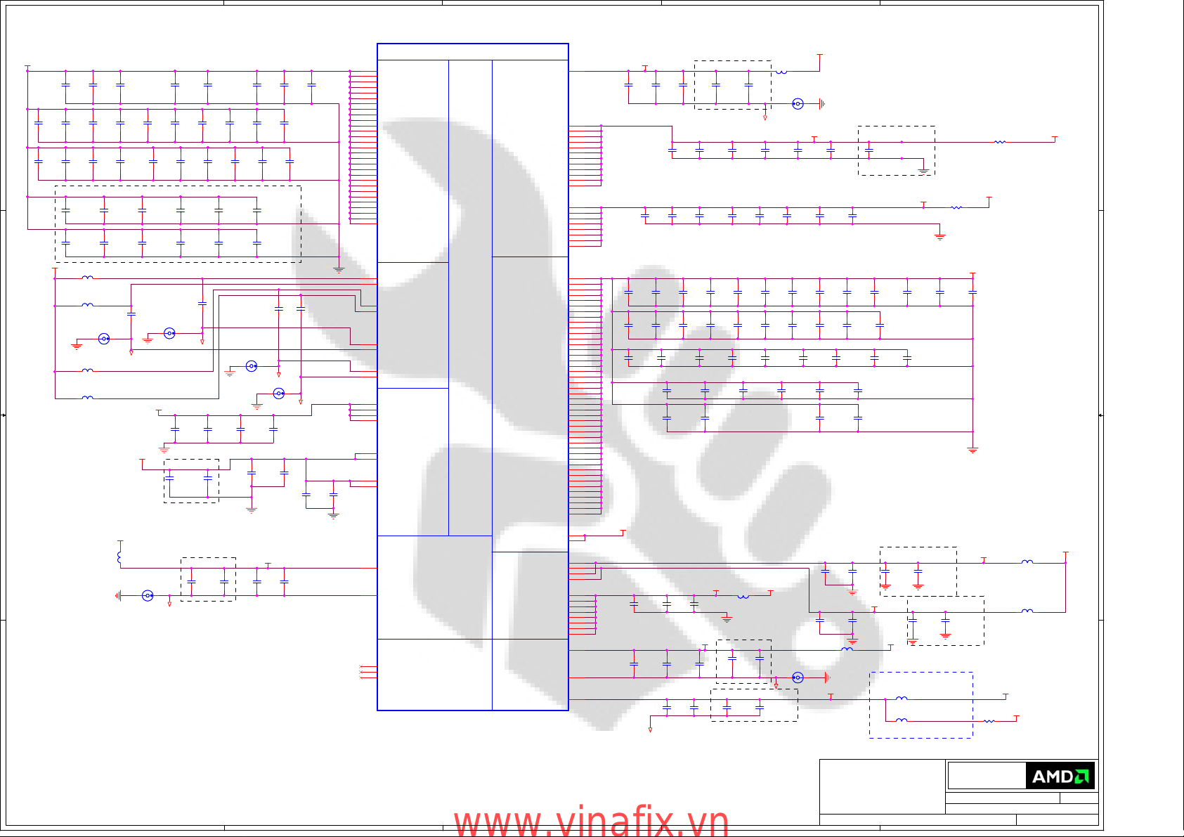
+12V_BUS
C1
10UFC110UF
+12V_BUS
+12V_BUS
+3.3V
C2
150nF_16VC2150nF_16V
C5
100nF_6.3VC5100nF_6.3V
D D
C C
B B
C3
150nF_16VC3150nF_16V
+3.3V
12
+
+
C4
C4
CD470u6.3EL11-RH-1
CD470u6.3EL11-RH-1
C6
1uF_6.3VC61uF_6.3V
+12V_BUS
12
+
+
C928
C928
CD470u16EL11.5
CD470u16EL11.5
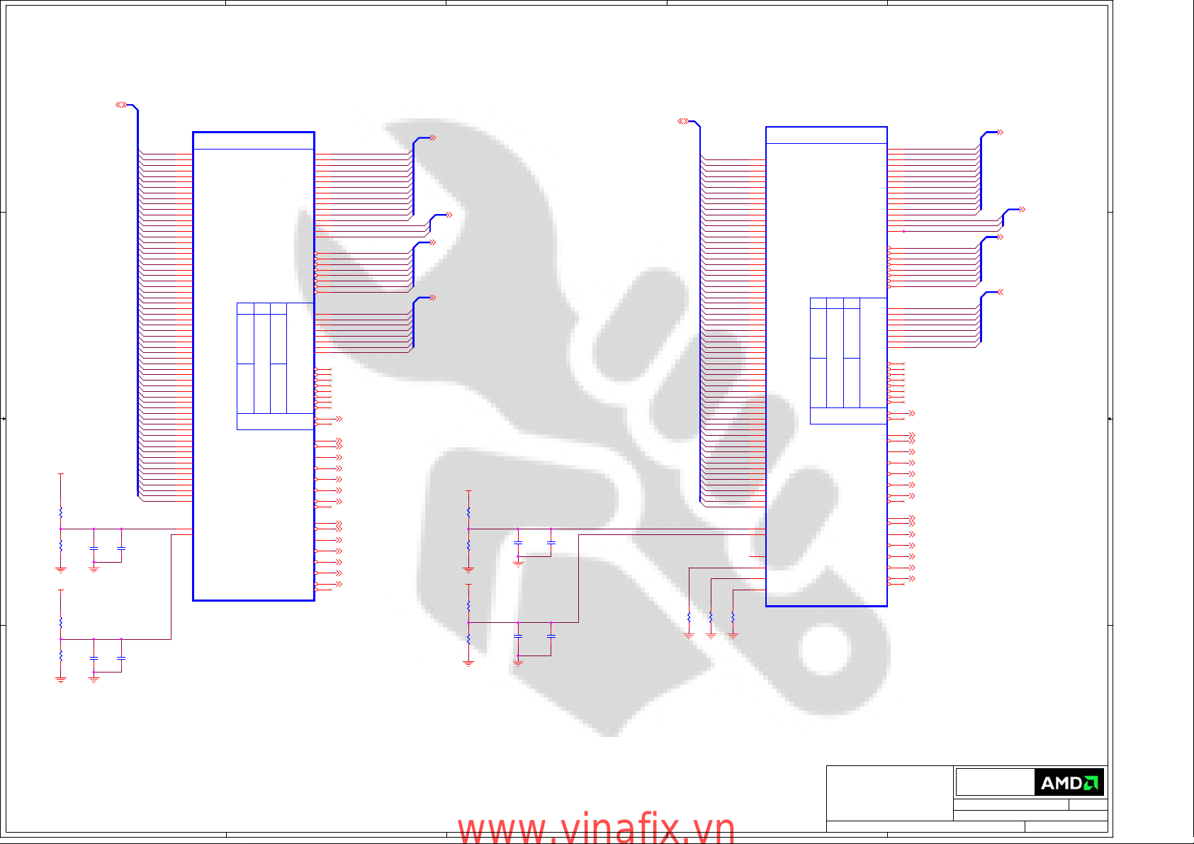
SMBCLK{7}
SMBDATA{7}
PETn0_GFXRn0{2}
PETp1_GFXRp1{2}
PETn1_GFXRn1{2}
PETp2_GFXRp2{2}
PETn2_GFXRn2{2}
PETp3_GFXRp3{2}
PETn3_GFXRn3{2}
PETp4_GFXRp4{2}
PETn4_GFXRn4{2}
PETp5_GFXRp5{2}
PETn5_GFXRn5{2}
PETp6_GFXRp6{2}
PETn6_GFXRn6{2}
PETp7_GFXRp7{2}
PETn7_GFXRn7{2}
PETp8_GFXRp8{2}
PETn8_GFXRn8{2}
PETp9_GFXRp9{2}
PETn9_GFXRn9{2}
PETp10_GFXRp10{2}
PETn10_GFXRn10{2}
PETp11_GFXRp11{2}
PETn11_GFXRn11{2}
PETp12_GFXRp12{2}
PETn12_GFXRn12{2}
PETp13_GFXRp13{2}
PETn13_GFXRn13{2}
PETp14_GFXRp14{2}
PETn14_GFXRn14{2}
PETp15_GFXRp15{2}
PETn15_GFXRn15{2}
TEST_EN_J
R10RR1
0R
PRESENCE
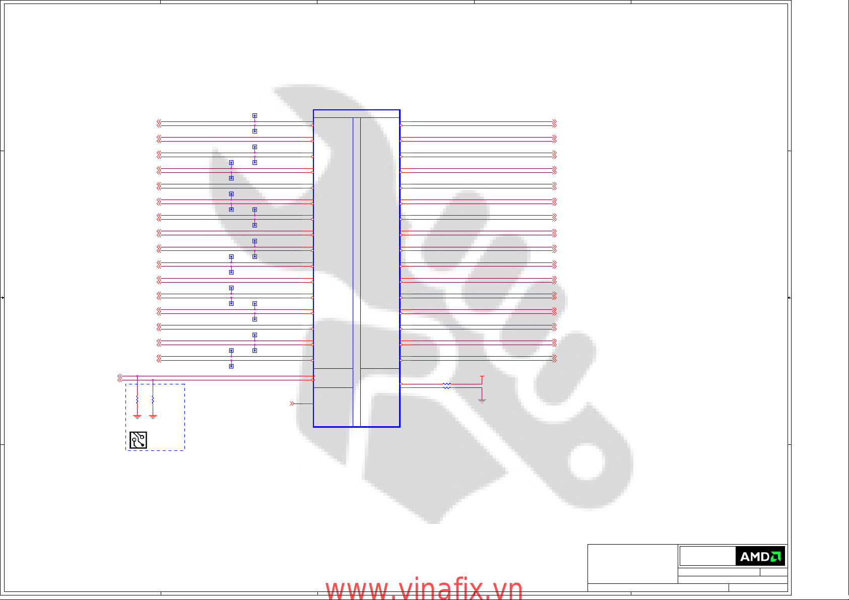
PCI-EXPRESS EDGE CONNECTOR
+3.3V_BUS
+12V_BUS
B1
B2
B3
B4
B5
B6
B7
B8
B9
B10
B11
B12
B13
B14
B15
B16
B17
B18
B19
B20
B21
B22
B23
B24
B25
B26
B27
B28
B29
B30
B31
B32
B33
B34
B35
B36
B37
B38
B39
B40
B41
B42
B43
B44
B45
B46
B47
B48
B49
B50
B51
B52
B53
B54
B55
B56
B57
B58
B59
B60
B61
B62
B63
B64
B65
B66
B67
B68
B69
B70
B71
B72
B73
B74
B75
B76
B77
B78
B79
B80
B81
B82
+12V#B1
+12V#B2
+12V#B3
GND#B4
SMCLK
SMDAT
GND#B7
+3.3V#B8
JTAG1
3.3Vaux
WAKE#
RSVD#B12
GND#B13
PETp0
PETn0
GND#B16
PRSNT2#B17
GND#B18
PETp1
PETn1
GND#B21
GND#B22
PETp2
PETn2
GND#B25
GND#B26
PETp3
PETn3
GND#B29
RSVD#B30
PRSNT2#B31
GND#B32
PETp4
PETn4
GND#B35
GND#B36
PETp5
PETn5
GND#B39
GND#B40
PETp6
PETn6
GND#B43
GND#B44
PETp7
PETn7
GND#B47
PRSNT2#B48
GND#B49
PETp8
PETn8
GND#B52
GND#B53
PETp9
PETn9
GND#B56
GND#B57
PETp10
PETn10
GND#B60
GND#B61
PETp11
PETn11
GND#B64
GND#B65
PETp12
PETn12
GND#B68
GND#B69
PETp13
PETn13
GND#B72
GND#B73
PETp14
PETn14
GND#B76
GND#B77
PETp15
PETn15
GND#B80
PRSNT2#B81
RSVD#B82
x16 PCIe
x16 PCIe
Mechanical Key
Mechanical Key
PRSNT1#A1
+12V#A2
+12V#A3
GND#A4
JTAG2
JTAG3
JTAG4
JTAG5
+3.3V#A9
+3.3V#A10
PERST#
GND#A12
REFCLK+
REFCLKGND#A15
PERp0
PERn0
GND#A18
RSVD#A19
GND#A20
PERp1
PERn1
GND#A23
GND#A24
PERp2
PERn2
GND#A27
GND#A28
PERp3
PERn3
GND#A31
RSVD#A32
RSVD#A33
GND#A34
PERp4
PERn4
GND#A37
GND#A38
PERp5
PERn5
GND#A41
GND#A42
PERp6
PERn6
GND#A45
GND#A46
PERp7
PERn7
GND#A49
RSVD#A50
GND#A51
PERp8
PERn8
GND#A54
GND#A55
PERp9
PERn9
GND#A58
GND#A59
PERp10
PERn10
GND#A62
GND#A63
PERp11
PERn11
GND#A66
GND#A67
PERp12
PERn12
GND#A70
GND#A71
PERp13
PERn13
GND#A74
GND#A75
PERp14
PERn14
GND#A78
GND#A79
PERp15
PERn15
GND#A82
MPCIE1
MPCIE1
A1
A2
A3
A4
A5
A6
A7
A8
A9
A10
A11
A12
A13
A14
A15
A16
A17
A18
A19
A20
A21
A22
A23
A24
A25
A26
A27
A28
A29
A30
A31
A32
A33
A34
A35
A36
A37
A38
A39
A40
A41
A42
A43
A44
A45
A46
A47
A48
A49
A50
A51
A52
A53
A54
A55
A56
A57
A58
A59
A60
A61
A62
A63
A64
A65
A66
A67
A68
A69
A70
A71
A72
A73
A74
A75
A76
A77
A78
A79
A80
A81
A82
PERp0
PERn0
PERp1
PERn1
PERp2
PERn2
PERp3
PERn3
PERp4
PERn4
PERp5
PERn5
PERp6
PERn6
PERp7
PERn7
PERp8
PERn8
PERp9
PERn9
PERp10
PERn10
PERp11
PERn11
PERp12
PERn12
PERp13
PERn13
PERp14
PERn14
PERp15
PERn15
+3.3V_BUS+12V_BUS
PRESENCE
JTDI
JTDO
C7
100nF_6.3VC7100nF_6.3V
C9
100nF_6.3VC9100nF_6.3V
C11
C11
100nF_6.3V
100nF_6.3V
C13
C13
100nF_6.3V
100nF_6.3V
C15
C15
100nF_6.3V
100nF_6.3V
C17
C17
100nF_6.3V
100nF_6.3V
C19
C19
100nF_6.3V
100nF_6.3V
C21
C21
100nF_6.3V
100nF_6.3V
C23
C23
100nF_6.3V
100nF_6.3V
C25
C25
100nF_6.3V
100nF_6.3V
C27
C27
100nF_6.3V
100nF_6.3V
C29
C29
100nF_6.3V
100nF_6.3V
C31
C31
100nF_6.3V
100nF_6.3V
C33
C33
100nF_6.3V
100nF_6.3V
C35
C35
100nF_6.3V
100nF_6.3V
C37
C37
100nF_6.3V
100nF_6.3V
PERST#
C8
100nF_6.3VC8100nF_6.3V
C10
C10
100nF_6.3V
100nF_6.3V
C12
C12
100nF_6.3V
100nF_6.3V
C14
C14
100nF_6.3V
100nF_6.3V
C16
C16
100nF_6.3V
100nF_6.3V
C18
C18
100nF_6.3V
100nF_6.3V
C20
C20
100nF_6.3V
100nF_6.3V
C22
C22
100nF_6.3V
100nF_6.3V
C24
C24
100nF_6.3V
100nF_6.3V
C26
C26
100nF_6.3V
100nF_6.3V
C28
C28
100nF_6.3V
100nF_6.3V
C30
C30
100nF_6.3V
100nF_6.3V
C32
C32
100nF_6.3V
100nF_6.3V
C34
C34
100nF_6.3V
100nF_6.3V
C36
C36
100nF_6.3V
100nF_6.3V
C38
C38
100nF_6.3V
100nF_6.3V
PCIE_REFCLKP {2}
PCIE_REFCLKN {2}PETp0_GFXRp0{2}
GFXTp0_PERp0 {2}
GFXTn0_PERn0 {2}
GFXTp1_PERp1 {2}
GFXTn1_PERn1 {2}
GFXTp2_PERp2 {2}
GFXTn2_PERn2 {2}
GFXTp3_PERp3 {2}
GFXTn3_PERn3 {2}
GFXTp4_PERp4 {2}
GFXTn4_PERn4 {2}
GFXTp5_PERp5 {2}
GFXTn5_PERn5 {2}
GFXTp6_PERp6 {2}
GFXTn6_PERn6 {2}
GFXTp7_PERp7 {2}
GFXTn7_PERn7 {2}
GFXTp8_PERp8 {2}
GFXTn8_PERn8 {2}
GFXTp9_PERp9 {2}
GFXTn9_PERn9 {2}
GFXTp10_PERp10 {2}
GFXTn10_PERn10 {2}
GFXTp11_PERp11 {2}
GFXTn11_PERn11 {2}
GFXTp12_PERp12 {2}
GFXTn12_PERn12 {2}
GFXTp13_PERp13 {2}
GFXTn13_PERn13 {2}
GFXTp14_PERp14 {2}
GFXTn14_PERn14 {2}
GFXTp15_PERp15 {2}
GFXTn15_PERn15 {2}
No JTAG
R2 0RR2 0R
+3.3V
53
1
2
R_RST
R3 0RR3 0R
Place R3 in U5
Table 1: Connection for JTAG
Production
(No JTAG)
Internal Use Only
TSW1 & R2 are located on the bottom side of the board close to PCIE connector.
Install R1 & R2 .Don't Install TSW1
Install TSW1 & Don't Install R2
TSW1 Switch #1, 2, 3, 4, 5 and 6 closed (ON)
JTAG
#7,8 open
TSW1 Switch #1, 2, 3, 4, 5 and 6 open
NO JTAG
#7,8 closed (ON)
C39
C39
100nF_6.3V
100nF_6.3V
NC7SZ08P5X_NL
NC7SZ08P5X_NL
4
U5
U5
PERST#_buf {2}
SYMBOL LEGEND
DO NOT
DNI
INSTALL
#
ACTIVE
LOW
DIGITAL
GROUND
ANALOG
A A
CONFIDENTIAL & PROPRIETARY TO ADVANCED MICRO DEVICES INC.
CONFIDENTIAL & PROPRIETARY TO ADVANCED MICRO DEVICES INC.
CONFIDENTIAL & PROPRIETARY TO ADVANCED MICRO DEVICES INC.
?2007 Advanced Micro Devices
?2007 Advanced Micro Devices
?2007 Advanced Micro Devices
This AMD Board schematic and design is the exclusive property of AMD,
This AMD Board schematic and design is the exclusive property of AMD,
This AMD Board schematic and design is the exclusive property of AMD,
and is provided only to entities under a non-disclosure agreement
and is provided only to entities under a non-disclosure agreement
and is provided only to entities under a non-disclosure agreement
with AMD for evaluation purposes. Further distribution or disclosure
with AMD for evaluation purposes. Further distribution or disclosure
with AMD for evaluation purposes. Further distribution or disclosure
is strictly prohibited. Use of this schematic and design for any purpose
is strictly prohibited. Use of this schematic and design for any purpose
is strictly prohibited. Use of this schematic and design for any purpose
other than evaluation requires a Board Technology License Agreement
other than evaluation requires a Board Technology License Agreement
other than evaluation requires a Board Technology License Agreement
with AMD. AMD makes no representations or warranties of any kind
with AMD. AMD makes no representations or warranties of any kind
with AMD. AMD makes no representations or warranties of any kind
regarding this schematic and design, including, not limited to,
regarding this schematic and design, including, not limited to,
regarding this schematic and design, including, not limited to,
any implied warranty of merchantibility or fitness for a particular
any implied warranty of merchantibility or fitness for a particular
any implied warranty of merchantibility or fitness for a particular
purpose, and disclaims responsibility forany consequences resulting
purpose, and disclaims responsibility forany consequences resulting
purpose, and disclaims responsibility forany consequences resulting
from use of the information included herein.
from use of the information included herein.
from use of the information included herein.
Title
Title
Title
RV635 DDR2 - PCI-E Edge Connector
RV635 DDR2 - PCI-E Edge Connector
8
7
6
5
www.vinafix.vn
4
3
RV635 DDR2 - PCI-E Edge Connector
2
Advanced Micro Devices Inc.
Advanced Micro Devices Inc.
Advanced Micro Devices Inc.
1 Commerce Valley Drive East
1 Commerce Valley Drive East
1 Commerce Valley Drive East
Markham, Ontario
Markham, Ontario
Markham, Ontario
Monday, March 24, 2008
Monday, March 24, 2008
Monday, March 24, 2008
Sheet
Sheet
Sheet
of
121
of
121
of
121
GROUND
BUO BRING UP
ONLY
Doc No.
Doc No.
Doc No.
105-B381xx-00A
105-B381xx-00A
105-B381xx-00A
1
RevDate:
RevDate:
RevDate:
0
0
0
Page 2
5
D D
NOTE: some of the PCIE testpoints will
be available trought via on traces.
PETp0_GFXRp0{1}
PETn0_GFXRn0{1}
PETp1_GFXRp1{1}
PETn1_GFXRn1{1}
PETp2_GFXRp2{1}
PETn2_GFXRn2{1}
PETp3_GFXRp3{1}
PETn3_GFXRn3{1}
PETp4_GFXRp4{1}
PETn4_GFXRn4{1}
PETp5_GFXRp5{1}
PETn5_GFXRn5{1}
PETp6_GFXRp6{1}
C C
B B
PCIE_REFCLKP{1}
PCIE_REFCLKN{1}
PETn6_GFXRn6{1}
PETp7_GFXRp7{1}
PETn7_GFXRn7{1}
PETp8_GFXRp8{1}
PETp9_GFXRp9{1}
PETn9_GFXRn9{1}
PETp10_GFXRp10{1}
PETn10_GFXRn10{1}
PETp11_GFXRp11{1}
PETn11_GFXRn11{1}
PETp12_GFXRp12{1}
PETn12_GFXRn12{1}
PETp13_GFXRp13{1}
PETn13_GFXRn13{1}
PETp14_GFXRp14{1}
PETn14_GFXRn14{1}
PETp15_GFXRp15{1}
PETn15_GFXRn15{1}
DNI DNI
R13
R13
R14
R14
51R
51R
51R
51R
402 402
TP11TP11
TP12TP12
TP13TP13
TP14TP14
TP19TP19
TP20TP20
TP21TP21
TP22TP22
TP27TP27
TP28TP28
4
U1A
TP7TP7
TP8TP8
TP9TP9
TP10TP10
TP15TP15
TP16TP16
TP17TP17
TP18TP18
TP23TP23
TP24TP24
TP25TP25
TP26TP26
U1A
AK33
AJ33
AJ35
AJ34
AH35
AH34
AG35
AG34
AF33
AE33
AE35
AE34
AD35
AD34
AC35
AC34
AB33
AA33
AA35
AA34
Y35
Y34
W35
W34
V33
U33
U35
U34
T35
T34
R35
R34
AJ31
AJ30
PERST#_buf{1}
AM32
PCIE_RX0P
PCIE_RX0N
PCIE_RX1P
PCIE_RX1N
PCIE_RX2P
PCIE_RX2N
PCIE_RX3P
PCIE_RX3N
PCIE_RX4P
PCIE_RX4N
PCIE_RX5P
PCIE_RX5N
PCIE_RX6P
PCIE_RX6N
PCIE_RX7P
PCIE_RX7N
PCIE_RX8P
PCIE_RX8N
PCIE_RX9P
PCIE_RX9N
PCIE_RX10P
PCIE_RX10N
PCIE_RX11P
PCIE_RX11N
PCIE_RX12P
PCIE_RX12N
PCIE_RX13P
PCIE_RX13N
PCIE_RX14P
PCIE_RX14N
PCIE_RX15P
PCIE_RX15N
Clock
Clock
PCIE_REFCLKP
PCIE_REFCLKN
PERSTB
PART 1 OF 7
PART 1 OF 7
P
P
C
C
I
I
-
E
E
X
X
P
P
R
R
E
E
S
S
S
S
I
I
N
N
T
T
E
E
R
R
F
F
A
A
C
C
E
E
PCIE_TX0P
PCIE_TX0N
PCIE_TX1P
PCIE_TX1N
PCIE_TX2P
PCIE_TX2N
PCIE_TX3P
PCIE_TX3N
PCIE_TX4P
PCIE_TX4N
PCIE_TX5P
PCIE_TX5N
PCIE_TX6P
PCIE_TX6N
PCIE_TX7P
PCIE_TX7N
PCIE_TX8P
PCIE_TX8N
PCIE_TX9P
PCIE_TX9N
PCIE_TX10P
PCIE_TX10N
PCIE_TX11P
PCIE_TX11N
PCIE_TX12P
PCIE_TX12N
PCIE_TX13P
PCIE_TX13N
PCIE_TX14P
PCIE_TX14N
PCIE_TX15P
PCIE_TX15N
Calibration
Calibration
PCIE_CALRN
PCIE_CALRP
3
AG31
AG30
AF31
AF30
AF28
AF27
AD31
AD30
AD28
AD27
AB31
AB30
AB28
AB27
AA31
AA30
AA28
AA27
W31
W30
W28
W27
V31
V30
V28
V27
U31
U30
U28
U27
R31
R30
+PCIE_VDDC
402
AG26
AJ27
R9
1.27KR91.27K
R82.0K R82.0K
402
2
GFXTp0_PERp0 {1}
GFXTn0_PERn0 {1}
GFXTp1_PERp1 {1}
GFXTn1_PERn1 {1}
GFXTp2_PERp2 {1}
GFXTn2_PERn2 {1}
GFXTp3_PERp3 {1}
GFXTn3_PERn3 {1}
GFXTp4_PERp4 {1}
GFXTn4_PERn4 {1}
GFXTp5_PERp5 {1}
GFXTn5_PERn5 {1}
GFXTp6_PERp6 {1}
GFXTn6_PERn6 {1}
GFXTp7_PERp7 {1}
GFXTn7_PERn7 {1}
GFXTp8_PERp8 {1}
GFXTn8_PERn8 {1}PETn8_GFXRn8{1}
GFXTp9_PERp9 {1}
GFXTn9_PERn9 {1}
GFXTp10_PERp10 {1}
GFXTn10_PERn10 {1}
GFXTp11_PERp11 {1}
GFXTn11_PERn11 {1}
GFXTp12_PERp12 {1}
GFXTn12_PERn12 {1}
GFXTp13_PERp13 {1}
GFXTn13_PERn13 {1}
GFXTp14_PERp14 {1}
GFXTn14_PERn14 {1}
GFXTp15_PERp15 {1}
GFXTn15_PERn15 {1}
1
For Tektronix LA only
Place close
to ASIC
A A
5
4
RV635 XT A11
RV635 XT A11
www.vinafix.vn
3
CONFIDENTIAL & PROPRIETARY TO ADVANCED MICRO DEVICES INC.
CONFIDENTIAL & PROPRIETARY TO ADVANCED MICRO DEVICES INC.
CONFIDENTIAL & PROPRIETARY TO ADVANCED MICRO DEVICES INC.
?2007 Advanced Micro Devices
?2007 Advanced Micro Devices
?2007 Advanced Micro Devices
This AMD Board schematic and design is the exclusive property of AMD,
This AMD Board schematic and design is the exclusive property of AMD,
This AMD Board schematic and design is the exclusive property of AMD,
and is provided only to entities under a non-disclosure agreement
and is provided only to entities under a non-disclosure agreement
and is provided only to entities under a non-disclosure agreement
with AMD for evaluation purposes. Further distribution or disclosure
with AMD for evaluation purposes. Further distribution or disclosure
with AMD for evaluation purposes. Further distribution or disclosure
is strictly prohibited. Use of this schematic and design for any purpose
is strictly prohibited. Use of this schematic and design for any purpose
is strictly prohibited. Use of this schematic and design for any purpose
other than evaluation requires a Board Technology License Agreement
other than evaluation requires a Board Technology License Agreement
other than evaluation requires a Board Technology License Agreement
with AMD. AMD makes no representations or warranties of any kind
with AMD. AMD makes no representations or warranties of any kind
with AMD. AMD makes no representations or warranties of any kind
regarding this schematic and design, including, not limited to,
regarding this schematic and design, including, not limited to,
regarding this schematic and design, including, not limited to,
any implied warranty of merchantibility or fitness for a particular
any implied warranty of merchantibility or fitness for a particular
any implied warranty of merchantibility or fitness for a particular
purpose, and disclaims responsibility forany consequences resulting
purpose, and disclaims responsibility forany consequences resulting
purpose, and disclaims responsibility forany consequences resulting
from use of the information included herein.
from use of the information included herein.
from use of the information included herein.
Title
Title
Title
RV635 DDR2 - ASIC PCIE_Interface
RV635 DDR2 - ASIC PCIE_Interface
2
RV635 DDR2 - ASIC PCIE_Interface
Advanced Micro Devices Inc.
Advanced Micro Devices Inc.
Advanced Micro Devices Inc.
1 Commerce Valley Drive East
1 Commerce Valley Drive East
1 Commerce Valley Drive East
Markham, Ontario
Markham, Ontario
Markham, Ontario
Monday, March 24, 2008
Monday, March 24, 2008
Monday, March 24, 2008
Sheet
Sheet
Sheet
of
221
of
221
of
221
1
Doc No.
Doc No.
Doc No.
RevDate:
RevDate:
RevDate:
0
0
0
105-B381xx-00A
105-B381xx-00A
105-B381xx-00A
Page 3

5
Recommended caps:
(see BOM for qualified values/vendors)
10uF , X6S, 0805, 6.3V, 1.4MM MAX THICK
1uF, X6S, 0402, 6.3V
100nF, X7R, 0402
10nF , X7R, 0402
D D
+1.8V
B889
B889
BLM15BD121SN1
BLM15BD121SN1
C C
LVT_EN{13}
+3.3V
R35
R35
4.7K
4.7K
I2C DEVICE ADDRESS' ON DDC2
B B
DEVICE
LM63
DP
A A
+1.8V
+3.3V
R36
R36
4.7K
4.7K
R42
R42
4.7K
4.7K
ADDRESS
x100 1100
TBD
+T2PVDD
Q100
Q100
SI2304DS
SI2304DS
1
R80
R80
4.7K
4.7K
T2XCM{15}
T2XCP{15}
T2X0M{15}
T2X0P{15}
T2X1M{15}
T2X1P{15}
T2X2M{15}
T2X2P{15}
T2X3M{15}
T2X3P{15}
T2X4M{15}
T2X4P{15}
T2X5M{15}
T2X5P{15}
MC100
NS100
NS100
NS_VIA
NS_VIA
1 2
Use 0R
B100
B100
32
BLM15BD121SN1
BLM15BD121SN1
DDC2DATA
DDC2CLK
CRT2DDCDATA{16}
CRT2DDCCLK{16}
What happens to all the JTAG resistors especially R7 and also the TRs?
MC100
4.7uF_6.3V
4.7uF_6.3V
GND_T2PVSS
Overlap footprints
MC103
MC103
4.7uF_6.3V
4.7uF_6.3V
R1090RR109
0R
+LTVDD33
+3.3V
R40
R40
4.7K
4.7K
402 402
SDA
SCL
MR71KMR7
1K
C103
C103
10uF_X6S
10uF_X6S
R41
R41
4.7K
4.7K
+1.8V
10uF_X6S
10uF_X6S
DDC2DATA
DDC2CLK
C100
C100
100nF_6.3V
100nF_6.3V
C108
C108
1uF_6.3V
1uF_6.3V
DNI for RV630
C107
C107
1uF_6.3V
1uF_6.3V
CRT1DDCDATA{15}
CRT1DDCCLK{15}
R43 221RR43 221R
R44 110RR44 110R
C101
C101
C109
C109
100nF_6.3V
100nF_6.3V
C46
C46
100nF_6.3V
100nF_6.3V
+LTVDD18
C105
C105
100nF_6.3V
100nF_6.3V
TEST_EN
HPD1{16}
T2XCM
T2XCP
T2X0M
T2X0P
T2X1M
T2X1P
T2X2M
T2X2P
T2X3M
T2X3P
T2X4M
T2X4P
T2X5M
T2X5P
C102
C102
1uF_6.3V
1uF_6.3V
VREFG
XTALIN
XTALOUT
4
AP22
AR22
AN22
AN23
AR23
AP23
AR24
AP24
AR25
AP25
AN26
AN27
AR27
AP27
AL22
AK22
AK27
AL27
AJ26
AH26
AJ22
AN21
AN24
AN25
AN28
AP21
AP26
AR21
AR26
AJ24
AM22
AM24
AM26
AM27
AM29
AL29
AJ15
AH15
AJ5
AJ4
AH14
AG14
AG6
AK6
AM6
AK4
AM4
AG21
AH19
AM30
AD12
AR33
AP33
Share one pad
U1B
U1B
Integrated
Integrated
LVTM/TMDS2
LVTM/TMDS2
T2XCM
T2XCP
T2X0M
T2X0P
T2X1M
T2X1P
T2X2M
T2X2P
T2X3M
T2X3P
T2X4M
T2X4P
T2X5M
T2X5P
T2PVDD
T2PVSS
T2XVDDC_1
T2XVDDC_2
T2XVDDR_1
T2XVDDR_2
T2XVSSR_1
T2XVSSR_2
T2XVSSR_3
T2XVSSR_4
T2XVSSR_5
T2XVSSR_6
T2XVSSR_7
T2XVSSR_8
T2XVSSR_9
T2XVSSR_10
T2XVSSR_11
T2XVSSR_12
T2XVSSR_13
T2XVSSR_14
Monitor
Monitor
DDC1DATA
Interface
Interface
DDC1CLK
DDC2DATA
DDC2CLK
DDC3DATA_DP3_AUXN
DDC3CLK_DP3_AUXP
DDC4DATA_DP4_AUXN
DDC4CLK_DP4_AUXP
HPD1
SDA
MMI2C
MMI2C
SCL
DMINUS
Thermal
Thermal
DPLUS
Diode
Diode
TS_FDO
PLLTEST
Test
Test
TESTEN
VREFG
XTALIN
XTALOUT
RV635 XT A11
RV635 XT A11
PART 2 OF 7
PART 2 OF 7
V
V
I
I
D
D
E
E
O
O
&
&
M
M
U
U
L
L
T
T
I
I
M
M
E
E
D
D
I
I
A
A
Integrated
Integrated
DP/TMDS
DP/TMDS
TXCAM_DPA3N
TXCAP_DPA3P
TX0M_DPA2N
TX0P_DPA2P
TX1M_DPA1N
TX1P_DPA1P
TX2M_DPA0N
TX2P_DPA0P
TXCBM_DPB3N
TXCBP_DPB3P
TX3M_DPB2N
TX3P_DPB2P
TX4M_DPB1N
TX4P_DPB1P
TX5M_DPB0N
TX5P_DPB0P
DPA_PVDD
DPA_PVSS
DPB_PVDD
DPB_PVSS
DPA_VDDR_1
DPA_VDDR_2
DPA_VSSR_1
DPA_VSSR_2
DPA_VSSR_3
DPA_VSSR_4
DPA_VSSR_5
DPB_VDDR_1
DPB_VDDR_2
DPB_VSSR_1
DPB_VSSR_2
DPB_VSSR_3
DPB_VSSR_4
DPB_VSSR_5
DAC / CRT
DAC / CRT
DAC2 (TV/CRT2)
DAC2 (TV/CRT2)
DP_CALR
HSYNC
VSYNC
RSET
AVDD
AVSSQ
VDD1DI
VSS1DI
H2SYNC
V2SYNC
COMP
R2SET
A2VDDQ
A2VSSQ
VDD2DI
VSS2DI
A2VDD
R116 182RR116 182R
AN9
AN10
R110 182RR110 182R
AR10
AP10
R111 182RR111 182R
AR11
AP11
R112 182RR112 182R
AR12
AP12
AR14
AP14
R113 182RR113 182R
AR15
AP15
R114 182RR114 182R
AR16
AP16
R115 182RR115 182R
AR17
AP17
DP_CALR
AG15
AM14
AL14
AH17
AG17
AP19
AR19
AN11
AN12
AN13
AN14
AN15
AN19
AN20
AN16
AN17
AN18
AR18
AP18
AR31
R
AP31
RB
AR30
G
AP30
GB
AR29
B
AP29
BB
AN29
AN30
AN31
AR32
AP32
AR28
AP28
AM19
R2
AL19
R2B
AM18
G2
AL18
G2B
AM17
B2
AL17
B2B
AM15
AL15
AK18
Y
AK19
C
AK17
R2SET GND_A2VSSQ
AJ21
AL21
AK21
AH22
AG22
AM21
C2030
C2030
10nF
10nF
3
R128 150RR128 150R
DNI for RV630
GND_DPAVSS
GND_DBPVSS
R1030 499RR1030 499R
C1023
C1023
10nF
10nF
R2030 715RR2030 715R
C2021
C2021
100nF_6.3V
100nF_6.3V
C2024
C2024
10nF
10nF
C2031
C2031
100nF_6.3V
100nF_6.3V
DPA_TX0P
DPA_TX0N
DPA_TX1P
DPA_TX1N
DPA_TX2P
DPA_TX2N
DPA_TX3P
DPA_TX3N
DPB_TX1P
DPB_TX1N
DPB_TX2P
DPB_TX2N
DPB_TX3P
DPB_TX3N
C111
C111
100nF
100nF
C190
C190
100nF
100nF
C115
C115
100nF
100nF
C193
C193
100nF
100nF
GND_AVSSQRSET
C2025
C2025
100nF_6.3V
100nF_6.3V
C2032
C2032
1uF_6.3V
1uF_6.3V
C1024
C1024
100nF_6.3V
100nF_6.3V
C2022
C2022
1uF_6.3V
1uF_6.3V
+VDD2DI
C2026
C2026
1uF_6.3V
1uF_6.3V
GND_VSS2DI
Overlap footprints
C112
C112
1uF_6.3V
1uF_6.3V
Overlap footprints
C191
C191
1uF_6.3V
1uF_6.3V
Overlap footprints
C116
C116
1uF_6.3V
1uF_6.3V
Overlap footprints
C194
C194
1uF_6.3V
1uF_6.3V
C1020
C1020
10nF
10nF
C1025
C1025
1uF_6.3V
1uF_6.3V
NS2021 NS_VIANS2021 NS_VIA
C1120 180nF_10VC1120 180nF_10V
C1122 180nF_10VC1122 180nF_10V
C1124 180nF_10VC1124 180nF_10V
C1126 180nF_10VC1126 180nF_10V
C1132 180nF_10VC1132 180nF_10V
C1134 180nF_10VC1134 180nF_10V
C1136 180nF_10VC1136 180nF_10V
C113
C113
10uF_X6S
10uF_X6S
C192
C192
10uF_X6S
10uF_X6S
C117
C117
10uF_X6S
10uF_X6S
C195
C195
10uF_X6S
10uF_X6S
C1021
C1021
100nF_6.3V
100nF_6.3V
+VDD1DI
NS1021 NS_VIANS1021 NS_VIA
GND_VSS1DI
12
C2033
C2033
10uF_X6S
10uF_X6S
C1121 180nF_10VC1121 180nF_10V
C1123 180nF_10VC1123 180nF_10V
C1125 180nF_10VC1125 180nF_10V
C1127 180nF_10VC1127 180nF_10V
C1133 180nF_10VC1133 180nF_10V
C1135 180nF_10VC1135 180nF_10V
C1137 180nF_10VC1137 180nF_10V
MC113
MC113
4.7uF_6.3V
4.7uF_6.3V
MC192
MC192
4.7uF_6.3V
4.7uF_6.3V
MC117
MC117
4.7uF_6.3V
4.7uF_6.3V
MC195
MC195
4.7uF_6.3V
4.7uF_6.3V
C1022
C1022
1uF_6.3V
1uF_6.3V
12
+A2VDDQ
NS2020 NS_VIANS2020 NS_VIA
GND_A2VSSQ
MC2033
MC2033
4.7uF_6.3V
4.7uF_6.3V
12
+A2VDD
+DPA_PVDD
+DPB_PVDD
+DPA_VDDR
+DPB_VDDR
+AVDD
NS1020 NS_VIANS1020 NS_VIA
B2030 26R_600mAB2030 26R_600mA
2
A_DAC1_R {15}
A_DAC1_RB {15}
A_DAC1_G {15}
A_DAC1_GB {15}
A_DAC1_B {15}
A_DAC1_BB {15}
12
GND_AVSSQ
A_DAC2_R {16}
A_DAC2_RB {16}
A_DAC2_G {16}
A_DAC2_GB {16}
A_DAC2_B {16}
A_DAC2_BB {16}
HSYNC_DAC2 {7,16}
VSYNC_DAC2 {7,16}
A_DAC2_Y {17}
A_DAC2_C {17}
A_DAC2_COMP {17}
B887 BLM15BD121SN1B887 BLM15BD121SN1
NS110
NS110
NS_VIA
NS_VIA
12
B890 BLM15BD121SN1B890 BLM15BD121SN1
NS190
NS190
NS_VIA
NS_VIA
12
+1.8V
B884
B884
BLM15BD121SN1
BLM15BD121SN1
+1.8V
B883
B883
BLM15BD121SN1
BLM15BD121SN1
+1.8V
B885
B885
BLM15BD121SN1
BLM15BD121SN1
+3.3V
R120 499RR120 499R
R122 499RR122 499R
R124 499RR124 499R
R126 499RR126 499R
R132 499RR132 499R
R134 499RR134 499R
R136 499RR136 499R
+1.8V
+1.8V
B881
B881
BLM15BD121SN1
BLM15BD121SN1
B892
B892
BLM15BD121SN1
BLM15BD121SN1
+1.1V
+1.1V
HSYNC_DAC1 {7,15}
VSYNC_DAC1 {7,15}
R121 499RR121 499R
R123 499RR123 499R
R125 499RR125 499R
R127 499RR127 499R
R133 499RR133 499R
R135 499RR135 499R
R137 499RR137 499R
DP_GND
LVT_EN{13}
1
1
+1.8V
B882
B882
BLM15BD121SN1
BLM15BD121SN1
32
Q110
Q110
SI2304DS
SI2304DS
T1XCM {16}
T1XCP {16}
T1X0M {16}
T1X0P {16}
T1X1M {16}
T1X1P {16}
T1X2M {16}
T1X2P {16}
T1X3M {16}
T1X3P {16}
T1X4M {16}
T1X4P {16}
T1X5M {16}
T1X5P {16}
Overlap footprints
CONFIDENTIAL & PROPRIETARY TO ADVANCED MICRO DEVICES INC.
CONFIDENTIAL & PROPRIETARY TO ADVANCED MICRO DEVICES INC.
C86
C86
EY82
EY82
22pF
22pF
27_MHZ
27_MHZ
2 1
C85
C85
22pF
22pF
5
R841MR84
1M
4
www.vinafix.vn
3
2
CONFIDENTIAL & PROPRIETARY TO ADVANCED MICRO DEVICES INC.
?2007 Advanced Micro Devices
?2007 Advanced Micro Devices
?2007 Advanced Micro Devices
This AMD Board schematic and design is the exclusive property of AMD,
This AMD Board schematic and design is the exclusive property of AMD,
This AMD Board schematic and design is the exclusive property of AMD,
and is provided only to entities under a non-disclosure agreement
and is provided only to entities under a non-disclosure agreement
and is provided only to entities under a non-disclosure agreement
with AMD for evaluation purposes. Further distribution or disclosure
with AMD for evaluation purposes. Further distribution or disclosure
with AMD for evaluation purposes. Further distribution or disclosure
is strictly prohibited. Use of this schematic and design for any purpose
is strictly prohibited. Use of this schematic and design for any purpose
is strictly prohibited. Use of this schematic and design for any purpose
other than evaluation requires a Board Technology License Agreement
other than evaluation requires a Board Technology License Agreement
other than evaluation requires a Board Technology License Agreement
with AMD. AMD makes no representations or warranties of any kind
with AMD. AMD makes no representations or warranties of any kind
with AMD. AMD makes no representations or warranties of any kind
regarding this schematic and design, including, not limited to,
regarding this schematic and design, including, not limited to,
regarding this schematic and design, including, not limited to,
any implied warranty of merchantibility or fitness for a particular
any implied warranty of merchantibility or fitness for a particular
any implied warranty of merchantibility or fitness for a particular
purpose, and disclaims responsibility forany consequences resulting
purpose, and disclaims responsibility forany consequences resulting
purpose, and disclaims responsibility forany consequences resulting
from use of the information included herein.
from use of the information included herein.
from use of the information included herein.
Title
Title
Title
RV635 DDR2 - ASIC MAIN
RV635 DDR2 - ASIC MAIN
RV635 DDR2 - ASIC MAIN
Advanced Micro Devices Inc.
Advanced Micro Devices Inc.
Advanced Micro Devices Inc.
1 Commerce Valley Drive East
1 Commerce Valley Drive East
1 Commerce Valley Drive East
Markham, Ontario
Markham, Ontario
Markham, Ontario
Monday, March 24, 2008
Monday, March 24, 2008
Monday, March 24, 2008
Sheet
Sheet
Sheet
of
321
of
321
of
321
1
Doc No.
Doc No.
Doc No.
RevDate:
RevDate:
RevDate:
0
0
0
105-B381xx-00A
105-B381xx-00A
105-B381xx-00A
Page 4
C151
C151
1uF_6.3V
1uF_6.3V
C131
C131
100nF_6.3V
100nF_6.3V
C141
C141
1uF_6.3V
1uF_6.3V
5
C152
C152
1uF_6.3V
1uF_6.3V
C132
C132
100nF_6.3V
100nF_6.3V
C142
C142
1uF_6.3V
1uF_6.3V
C133
C133
100nF_6.3V
100nF_6.3V
C143
C143
1uF_6.3V
1uF_6.3V
C154
C154
1uF_6.3V
1uF_6.3V
C134
C134
100nF_6.3V
100nF_6.3V
C144
C144
1uF_6.3V
1uF_6.3V
C155
C155
1uF_6.3V
1uF_6.3V
C135
C135
100nF_6.3V
100nF_6.3V
C145
C145
1uF_6.3V
1uF_6.3V
C136
C136
100nF_6.3V
100nF_6.3V
C146
C146
1uF_6.3V
1uF_6.3V
C157
C157
1uF_6.3V
1uF_6.3V
C137
C137
100nF_6.3V
100nF_6.3V
C147
C147
1uF_6.3V
1uF_6.3V
C158
C158
1uF_6.3V
1uF_6.3V
C138
C138
100nF_6.3V
100nF_6.3V
Recommended caps:
(see BOM for qualified values/vendors)
10uF , X6S, 0805, 6.3V, 1.4MM MAX THICK
1uF, X6S, 0402, 6.3V
100nF, X7R, 0402
10nF , X7R, 0402
+MVDD
C150
C150
1uF_6.3V
1uF_6.3V
D D
C156
C156
100nF_6.3V
100nF_6.3V
C153
C153
1uF_6.3V
1uF_6.3V
C130
C130
100nF_6.3V
100nF_6.3V
C140
C140
1uF_6.3V
1uF_6.3V
Overlap cap pair foorprints (0805 with 0603)
C127
C124
10uF_X6S
10uF_X6S
10uF_X6S
10uF_X6S
MC125
MC125
MC124
MC124
4.7uF_6.3V
4.7uF_6.3V
4.7uF_6.3V
4.7uF_6.3V
+MVDD
B120
B120
BLM15BD121SN1
BLM15BD121SN1
B121
B121
BLM15BD121SN1
C C
B B
A A
BLM15BD121SN1
NS121 NS_VIANS121 NS_VIA
1 2
GND_VSSRHA_2
B122
B122
BLM15BD121SN1
BLM15BD121SN1
B123
B123
BLM15BD121SN1
BLM15BD121SN1
+1.8V
B886
B886
BLM15BD121SN1
BLM15BD121SN1
NS70 NS_VIANS70 NS_VIA
GND_PVSS
C121
C121
1uF_6.3V
1uF_6.3V
+1.8V
1 2
10uF_X6S
10uF_X6S
10uF_X6S
10uF_X6S
MC126
MC126
MC127
MC127
4.7uF_6.3V
4.7uF_6.3V
4.7uF_6.3V
4.7uF_6.3V
C120
C120
1uF_6.3V
1uF_6.3V
NS120 NS_VIANS120 NS_VIA
1 2
GND_VSSRHA_1
+3.3V
C90
C90
1uF_6.3V
1uF_6.3V
Overlap footprints
MC94
MC94
4.7uF_6.3V
4.7uF_6.3V
Overlap footprints
MC70
MC70
4.7uF_6.3V
4.7uF_6.3V
C91
C91
100nF_6.3V
100nF_6.3V
C94
C94
10uF_X6S
10uF_X6S
C127
C126
C126
C125
C125
C124
C128
C128
10uF_X6S
10uF_X6S
MC128
MC128
4.7uF_6.3V
4.7uF_6.3V
C122
C122
1uF_6.3V
1uF_6.3V
NS122 NS_VIANS122 NS_VIA
1 2
GND_VSSRHB_1
C92
C92
1uF_6.3V
1uF_6.3V
+DPLL_PVDD
C70
C70
10uF_X6S
10uF_X6S
C129
C129
10uF_X6S
10uF_X6S
MC129
MC129
4.7uF_6.3V
4.7uF_6.3V
NS123 NS_VIANS123 NS_VIA
1 2
GND_VSSRHB_2
C93
C93
100nF_6.3V
100nF_6.3V
C95
C95
1uF_6.3V
1uF_6.3V
C71
C71
100nF_6.3V
100nF_6.3V
C97
C97
100nF_6.3V
100nF_6.3V
C72
C72
1uF_6.3V
1uF_6.3V
C148
C148
1uF_6.3V
1uF_6.3V
C123
C123
1uF_6.3V
1uF_6.3V
C96
C96
1uF_6.3V
1uF_6.3V
C159
C159
1uF_6.3V
1uF_6.3V
+DPLL_PVDD
GND_PVSS
4
C98
C98
100nF_6.3V
100nF_6.3V
AE14
AE15
AE17
AF12
AR20
AP20
AR35
H35
L22
M10
M35
P10
A12
A16
A20
A24
A28
B35
D35
K10
K12
K24
K26
L14
L15
L17
L18
L19
L21
A25
A32
B25
B32
AP2
AR2
AN1
AP1
A35
AR1
U1E
U1E
A8
M1
T1
Y1
B1
D1
H1
B2
L1
C2
L2
RV635 XT A11
RV635 XT A11
VDDR1_1
VDDR1_2
VDDR1_3
VDDR1_4
VDDR1_5
VDDR1_6
VDDR1_7
VDDR1_8
VDDR1_9
VDDR1_10
VDDR1_11
VDDR1_12
VDDR1_13
VDDR1_14
VDDR1_15
VDDR1_16
VDDR1_17
VDDR1_18
VDDR1_19
VDDR1_20
VDDR1_21
VDDR1_22
VDDR1_23
VDDR1_24
VDDR1_25
VDDR1_26
VDDR1_27
VDDR1_28
VDDR1_29
VDDRHA_1
VDDRHA_2
VDDRHB_1
VDDRHB_2
VSSRHA_1
VSSRHA_2
VSSRHB_1
VSSRHB_2
VDDR3_1
VDDR3_2
VDDR3_3
VDDR3_4
VDDR4_1
VDDR4_2
VDDR5_1
VDDR5_2
DPLL_PVDD
DPLL_PVSS
MECH_1
MECH_2
MECH_3
PART 5 OF 7
PART 5 OF 7
Memory I/O
Memory I/O
Selected PLL's
Selected PLL's
Mechanical Pins
Mechanical Pins
3
+MPVDD
GND_MPVSS
+DPLL_VDDC
+PCIE_PVDD
C930
C930
10nF
10nF
C900
C900
10nF
10nF
C161
C161
1uF_6.3V
1uF_6.3V
C171
C171
1uF_6.3V
1uF_6.3V
C160
C160
1uF_6.3V
1uF_6.3V
Overlap cap pair foorprints (0805 with 0603)
+VDDC
C78
C78
1uF_6.3V
1uF_6.3V
C65
C65
C64
C64
100nF_6.3V
100nF_6.3V
10nF
10nF
GND_PVSS
AM35
PCIE_PVDD
R26
PCIE_VDDC_1
W25
PCIE_VDDC_2
W26
PCIE_VDDC_3
AA25
PCIE_VDDC_4
AA26
PCIE_VDDC_5
AB25
PCIE_VDDC_6
AB26
PCIE_VDDC_7
AD26
PCIE_VDDC_8
AF26
PCIE_VDDC_9
U26
PCIE_VDDC_10
V25
PCIE_VDDC_11
V26
PCIE_VDDC_12
AL33
PCIE_VDDR_1
AM33
PCIE_VDDR_2
AN33
PCIE_VDDR_3
AN34
PCIE_VDDR_4
AN35
PCIE_VDDR_5
AP34
PCIE_VDDR_6
AP35
PCIE_VDDR_7
AR34
P
P
O
O
W
W
E
E
R
R
PCIE_VDDR_8
N13
VDDC_1
Core PCI-Express
Core PCI-Express
VDDC_2
VDDC_3
VDDC_4
VDDC_5
VDDC_6
VDDC_7
VDDC_8
VDDC_9
VDDC_10
VDDC_11
VDDC_12
VDDC_13
VDDC_14
VDDC_15
VDDC_16
VDDC_17
VDDC_18
VDDC_19
VDDC_20
VDDC_21
VDDC_22
VDDC_23
VDDC_24
VDDC_25
VDDC_26
VDDC_27
VDDC_28
VDDC_29
VDDC_30
VDDC_31
VDDC_32
VDDC_33
VDDC_34
VDDC_35
VDDC_36
VDDC_37
VDDC_38
VDDC_39
VDDC_40
VDDC_41
VDDC_42
VDDC_43
VDDC_44
BBP_1
BBP_2
VDDCI_1
VDDCI_2
VDDCI_3
VDDCI_4
VDD_CT_1
VDD_CT_2
VDD_CT_3
VDD_CT_4
VDD_CT_5
VDD_CT_6
VDD_CT_7
VDD_CT_8
MPVDD
MPVSS
DPLL_VDDC
R18
W11
AB19
AC23
AE18
AE19
AE21
AE22
N15
N18
N21
N23
P14
P17
P19
P22
R13
R15
R21
R23
U14
U17
U19
U22
V15
V18
V21
V23
W14
W17
W19
W22
AA15
AA18
AA21
AA23
AB14
AB17
AB22
AC13
AC15
AC18
AC21
U13
V13
M12
M24
P11
P25
R11
R25
U11
U25
AA11
AB11
AD10
AF10
A14
B15
AG19
C931
C931
100nF_6.3V
100nF_6.3V
C162
C162
1uF_6.3V
1uF_6.3V
C172
C172
1uF_6.3V
1uF_6.3V
C184
C184
1uF_6.3V
1uF_6.3V
C181
C181
10uF_X6S
10uF_X6S
MC181
MC181
4.7uF_6.3V
4.7uF_6.3V
C68
C68
1uF_6.3V
1uF_6.3V
1uF_6.3V
1uF_6.3V
C61
C61
100nF_6.3V
100nF_6.3V
Overlap footprints
C932
C932
1uF_6.3V
1uF_6.3V
C920
C920
1uF_6.3V
1uF_6.3V
C901
C901
100nF_6.3V
100nF_6.3V
C163
C163
1uF_6.3V
1uF_6.3V
C173
C173
1uF_6.3V
1uF_6.3V
C69
C69
100nF_6.3V
100nF_6.3V
+MPVDD
C66
C66
C62
C62
1uF_6.3V
1uF_6.3V
C933
C933
10uF_X6S
10uF_X6S
C921
C921
1uF_6.3V
1uF_6.3V
C902
C902
1uF_6.3V
1uF_6.3V
C164
C164
1uF_6.3V
1uF_6.3V
C174
C174
1uF_6.3V
1uF_6.3V
C185
C185
1uF_6.3V
1uF_6.3V
C182
C182
10uF_X6S
10uF_X6S
MC182
MC182
4.7uF_6.3V
4.7uF_6.3V
+VDD_CT
BLM15BD121SN1
BLM15BD121SN1
Overlap footprints
C67
C67
10uF_X6S
10uF_X6S
Overlap footprints
C922
C922
1uF_6.3V
1uF_6.3V
C903
C903
10nF
10nF
C165
C165
1uF_6.3V
1uF_6.3V
C175
C175
1uF_6.3V
1uF_6.3V
C186
C186
1uF_6.3V
1uF_6.3V
B69
B69
C63
C63
10uF_X6S
10uF_X6S
MC933
MC933
4.7uF_6.3V
4.7uF_6.3V
C183
C183
10uF_X6S
10uF_X6S
2
B930
B930
BLM15BD121SN1
BLM15BD121SN1
NS18 NS_VIANS18 NS_VIA
GND_PCIE_PVSS
C923
C923
1uF_6.3V
1uF_6.3V
C904
C904
100nF_6.3V
100nF_6.3V
C166
C166
1uF_6.3V
1uF_6.3V
C176
C176
1uF_6.3V
1uF_6.3V
C944
C944
1uF_6.3V
1uF_6.3V
+1.8V
MC67
MC67
4.7uF_6.3V
4.7uF_6.3V
MC63
MC63
4.7uF_6.3V
4.7uF_6.3V
+PCIE_VDDC
C924
C924
1uF_6.3V
1uF_6.3V
C905
C905
1uF_6.3V
1uF_6.3V
C167
C167
1uF_6.3V
1uF_6.3V
C177
C177
1uF_6.3V
1uF_6.3V
C187
C187
10uF_X6S
10uF_X6S
NS64NS_VIA NS64NS_VIA
GND_MPVSS
+1.8V
12
C925
C925
1uF_6.3V
1uF_6.3V
C906
C906
1uF_6.3V
1uF_6.3V
C168
C168
1uF_6.3V
1uF_6.3V
C178
C178
1uF_6.3V
1uF_6.3V
C946
C946
C945
C945
1uF_6.3V
1uF_6.3V
1uF_6.3V
1uF_6.3V
C188
C188
10uF_X6S
10uF_X6S
MC188
MC188
4.7uF_6.3V
4.7uF_6.3V
C74
C74
100nF_6.3V
100nF_6.3V
C73
C73
100nF_6.3V
100nF_6.3V
B67 60R_700mAB67 60R_700mA
12
+DPLL_VDDC
Overlap footprints
C926
C926
10uF_X6S
10uF_X6S
C907
C907
1uF_6.3V
1uF_6.3V
C169
C169
C170
C170
1uF_6.3V
1uF_6.3V
1uF_6.3V
1uF_6.3V
C179
C179
C180
C180
1uF_6.3V
1uF_6.3V
1uF_6.3V
1uF_6.3V
C947
C947
1uF_6.3V
1uF_6.3V
C189
C189
10uF_X6S
10uF_X6S
MC189
MC189
4.7uF_6.3V
4.7uF_6.3V
Overlap footprints
C77
C77
C75
C75
10uF_X6S
10uF_X6S
1uF_6.3V
1uF_6.3V
+VDDCI_2
C76
C76
1uF_6.3V
1uF_6.3V
+VDDC
Install only one of these two
+PCIE_VDDR
C942
C942
C941
C941
1uF_6.3V
1uF_6.3V
1uF_6.3V
1uF_6.3V
C948
C948
1uF_6.3V
1uF_6.3V
MC77
MC77
4.7uF_6.3V
4.7uF_6.3V
Overlap footprints
C79
C79
10uF_X6S
10uF_X6S
B60
B60
BLM15BD121SN1
BLM15BD121SN1
MB60
MB60
BLM15BD121SN1
BLM15BD121SN1
R9000RR900
0R
MC79
MC79
4.7uF_6.3V
4.7uF_6.3V
+VDDC
+1.8V
C943
C943
1uF_6.3V
1uF_6.3V
+VDDCI_1
R922
R922
1
B9200RB920
0R
B77 220R_2AB77 220R_2A
B78 220R_2AB78 220R_2A
+1.1V
+VDDC
1.5R
1.5R
+1.1V
+VDDC
CONFIDENTIAL & PROPRIETARY TO ADVANCED MICRO DEVICES INC.
CONFIDENTIAL & PROPRIETARY TO ADVANCED MICRO DEVICES INC.
CONFIDENTIAL & PROPRIETARY TO ADVANCED MICRO DEVICES INC.
?2007 Advanced Micro Devices
?2007 Advanced Micro Devices
?2007 Advanced Micro Devices
This AMD Board schematic and design is the exclusive property of AMD,
This AMD Board schematic and design is the exclusive property of AMD,
This AMD Board schematic and design is the exclusive property of AMD,
and is provided only to entities under a non-disclosure agreement
and is provided only to entities under a non-disclosure agreement
and is provided only to entities under a non-disclosure agreement
with AMD for evaluation purposes. Further distribution or disclosure
with AMD for evaluation purposes. Further distribution or disclosure
with AMD for evaluation purposes. Further distribution or disclosure
is strictly prohibited. Use of this schematic and design for any purpose
is strictly prohibited. Use of this schematic and design for any purpose
is strictly prohibited. Use of this schematic and design for any purpose
other than evaluation requires a Board Technology License Agreement
other than evaluation requires a Board Technology License Agreement
other than evaluation requires a Board Technology License Agreement
with AMD. AMD makes no representations or warranties of any kind
with AMD. AMD makes no representations or warranties of any kind
with AMD. AMD makes no representations or warranties of any kind
regarding this schematic and design, including, not limited to,
regarding this schematic and design, including, not limited to,
regarding this schematic and design, including, not limited to,
any implied warranty of merchantibility or fitness for a particular
any implied warranty of merchantibility or fitness for a particular
any implied warranty of merchantibility or fitness for a particular
purpose, and disclaims responsibility forany consequences resulting
purpose, and disclaims responsibility forany consequences resulting
purpose, and disclaims responsibility forany consequences resulting
from use of the information included herein.
from use of the information included herein.
from use of the information included herein.
Title
Title
Title
RV635 DDR2 - ASIC Power
RV635 DDR2 - ASIC Power
5
4
www.vinafix.vn
3
2
RV635 DDR2 - ASIC Power
Advanced Micro Devices Inc.
Advanced Micro Devices Inc.
Advanced Micro Devices Inc.
1 Commerce Valley Drive East
1 Commerce Valley Drive East
1 Commerce Valley Drive East
Markham, Ontario
Markham, Ontario
Markham, Ontario
Monday, March 24, 2008
Monday, March 24, 2008
Monday, March 24, 2008
Sheet
Sheet
Sheet
of
421
of
421
of
421
1
Doc No.
Doc No.
Doc No.
RevDate:
RevDate:
RevDate:
0
0
0
105-B381xx-00A
105-B381xx-00A
105-B381xx-00A
Page 5
5
4
3
2
1
+MVDD
+MVDD
R291
R291
100R
100R
1%
R292
R292
100R
100R
1%
R293
R293
100R
100R
1%
R294
R294
100R
100R
1%
DQA_[63..0]{8}
C291
C291
100nF
100nF
C293
C293
100nF
100nF
C292
C292
10nF
10nF
C294
C294
10nF
10nF
DQA_0
DQA_1
DQA_2
DQA_3
DQA_4
DQA_5
DQA_6
DQA_7
DQA_8
DQA_9
DQA_10
DQA_11
DQA_12
DQA_13
DQA_14
DQA_15
DQA_16
DQA_17
DQA_18
DQA_19
DQA_20
DQA_21
DQA_22
DQA_23
DQA_24
DQA_25
DQA_26
DQA_27
DQA_28
DQA_29
DQA_30
DQA_31
DQA_32
DQA_33
DQA_34
DQA_35
DQA_36
DQA_37
DQA_38
DQA_39
DQA_40
DQA_41
DQA_42
DQA_43
DQA_44
DQA_45
DQA_46
DQA_47
DQA_48
DQA_49
DQA_50
DQA_51
DQA_52
DQA_53
DQA_54
DQA_55
DQA_56
DQA_57
DQA_58
DQA_59
DQA_60
DQA_61
DQA_62
DQA_63
MVREFS_0
P27
P28
P31
P32
M27
K29
K31
K32
M33
M34
L34
L35
J33
J34
H33
H34
K27
J29
J30
J31
F29
F32
D30
D32
G33
G34
G35
F34
D34
C34
C35
B34
C24
B24
B23
A23
C21
B21
C20
B20
J22
H22
F22
D21
J19
G19
F19
D19
C19
B19
A19
B18
C16
B16
C15
A15
H18
F18
E18
D18
J17
G15
E15
D15
N35
N34
U1C
U1C
DQA_0
DQA_1
DQA_2
DQA_3
DQA_4
DQA_5
DQA_6
DQA_7
DQA_8
DQA_9
DQA_10
DQA_11
DQA_12
DQA_13
DQA_14
DQA_15
DQA_16
DQA_17
DQA_18
DQA_19
DQA_20
DQA_21
DQA_22
DQA_23
DQA_24
DQA_25
DQA_26
DQA_27
DQA_28
DQA_29
DQA_30
DQA_31
DQA_32
DQA_33
DQA_34
DQA_35
DQA_36
DQA_37
DQA_38
DQA_39
DQA_40
DQA_41
DQA_42
DQA_43
DQA_44
DQA_45
DQA_46
DQA_47
DQA_48
DQA_49
DQA_50
DQA_51
DQA_52
DQA_53
DQA_54
DQA_55
DQA_56
DQA_57
DQA_58
DQA_59
DQA_60
DQA_61
DQA_62
DQA_63
MVREFDA
MVREFSA
RV635 XT A11
RV635 XT A11
Part 3 of 7
Part 3 of 7
MEMORY INTERFACE A
MEMORY INTERFACE A
DDR1 DDR2 DDR3
DDR1 DDR2 DDR3
bidir. differential strobe
write strobe
bidir. differential strobe
write strobe
Not used
Not used
For DDR2
For DDR2
read strobe
read strobe
bidir. strobe
bidir. strobe
MAA_0
MAA_1
MAA_2
MAA_3
MAA_4
MAA_5
MAA_6
MAA_7
MAA_8
MAA_9
MAA_10
MAA_11
MAA_A12
MAA_BA0
MAA_BA1
MAA_BA2
DQMAB_0
DQMAB_1
DQMAB_2
DQMAB_3
DQMAB_4
DQMAB_5
DQMAB_6
DQMAB_7
QSA_0
QSA_1
QSA_2
QSA_3
QSA_4
QSA_5
QSA_6
QSA_7
QSA_0B
QSA_1B
QSA_2B
QSA_3B
QSA_4B
QSA_5B
QSA_6B
QSA_7B
ODTA0
ODTA1
CLKA0
CLKA0B
CKEA0
RASA0B
CASA0B
WEA0B
CSA0B_0
CSA0B_1
CLKA1
CLKA1B
CKEA1
RASA1B
CASA1B
WEA1B
CSA1B_0
CSA1B_1
DQB_[63..0]{9}
MAA_0
C27
MAA_1
B28
MAA_2
B27
MAA_3
G26
MAA_4
F27
MAA_5
E27
MAA_6
D27
MAA_7
J27
MAA_8
E29
MAA_9
C30
MAA_10
E26
MAA_11
A27
MAA_12
G27
MAA_BA0
C28
MAA_BA1
B29
MAA_BA2
D26
DQMAb_0
M29
DQMAb_1
K33
DQMAb_2
G30
DQMAb_3
E33
DQMAb_4
C22
DQMAb_5
H21
DQMAb_6
C17
DQMAb_7
G17
QSA_0
M30
QSA_1
K34
QSA_2
G31
QSA_3
E34
QSA_4
B22
QSA_5
F21
QSA_6
B17
QSA_7
D17
M31
K35
G32
E35
A22
E21
A17
E17
C31
ODTA0 {8}
C25
A33
CLKA0 {8}
B33
CLKA0b {8}
B31
CKEA0 {8}
A31
RASA0b {8}
C32
CASA0b {8}
C29
WEA0b {8}
A30
CSA0b_0 {8}
B30
A26
CLKA1 {8}
B26
CLKA1b {8}
F24
CKEA1 {8}
D24
RASA1b {8}
H26
CASA1b {8}
D22
WEA1b {8}
G24
CSA1b_0 {8}
H24
MAA_[12..0] {8}
MAA_BA[2..0] {8}
DQMAb_[7..0] {8}
QSA_[7..0] {8}
+MVDD
+MVDD
R391
R391
100R
100R
1%
R392
R392
100R
100R
1%
R393
R393
100R
100R
1%
R394
R394
100R
100R
1%
C391
C391
100nF
100nF
C393
C393
100nF
100nF
C392
C392
10nF
10nF
C394
C394
10nF
10nF
MVREFD_1MVREFD_0
MVREFS_1
R296
R296
4.7K
4.7K
DQB_0
DQB_1
DQB_2
DQB_3
DQB_4
DQB_5
DQB_6
DQB_7
DQB_8
DQB_9
DQB_10
DQB_11
DQB_12
DQB_13
DQB_14
DQB_15
DQB_16
DQB_17
DQB_18
DQB_19
DQB_20
DQB_21
DQB_22
DQB_23
DQB_24
DQB_25
DQB_26
DQB_27
DQB_28
DQB_29
DQB_30
DQB_31
DQB_32
DQB_33
DQB_34
DQB_35
DQB_36
DQB_37
DQB_38
DQB_39
DQB_40
DQB_41
DQB_42
DQB_43
DQB_44
DQB_45
DQB_46
DQB_47
DQB_48
DQB_49
DQB_50
DQB_51
DQB_52
DQB_53
DQB_54
DQB_55
DQB_56
DQB_57
DQB_58
DQB_59
DQB_60
DQB_61
DQB_62
DQB_63
R297
R297
4.7K
4.7K
R298
R298
243R
243R
H15
G14
E14
D14
H12
G12
F12
D10
B13
C12
B12
B11
C9
B9
A9
B8
J10
H10
F10
D9
G7
G6
F6
D6
C8
C7
B7
A7
B5
A5
C4
B4
M3
M2
N2
N1
R3
R2
T3
T2
M8
M7
P5
P4
R9
R8
R6
U4
U3
U2
U1
V2
Y3
Y2
AA2
AA1
U9
U7
U6
V4
W9
W7
W6
W4
B14
A13
AA4
AA8
AA7
AA5
U1D
U1D
DQB_0
DQB_1
DQB_2
DQB_3
DQB_4
DQB_5
DQB_6
DQB_7
DQB_8
DQB_9
DQB_10
DQB_11
DQB_12
DQB_13
DQB_14
DQB_15
DQB_16
DQB_17
DQB_18
DQB_19
DQB_20
DQB_21
DQB_22
DQB_23
DQB_24
DQB_25
DQB_26
DQB_27
DQB_28
DQB_29
DQB_30
DQB_31
DQB_32
DQB_33
DQB_34
DQB_35
DQB_36
DQB_37
DQB_38
DQB_39
DQB_40
DQB_41
DQB_42
DQB_43
DQB_44
DQB_45
DQB_46
DQB_47
DQB_48
DQB_49
DQB_50
DQB_51
DQB_52
DQB_53
DQB_54
DQB_55
DQB_56
DQB_57
DQB_58
DQB_59
DQB_60
DQB_61
DQB_62
DQB_63
MVREFDB
MVREFSB
DRAM_RST
TEST_MCLK
TEST_YCLK
MEMTEST
RV635 XT A11
RV635 XT A11
Part 4 of 7
Part 4 of 7
MEMORY INTERFACE B
MEMORY INTERFACE B
DDR1 DDR2 DDR3
DDR1 DDR2 DDR3
write strobe
write strobe
Not used
Not used
bidir. differential strobe
bidir. differential strobe
For DDR2
For DDR2
bidir. strobe
read strobe
bidir. strobe
read strobe
MAB_0
MAB_1
MAB_2
MAB_3
MAB_4
MAB_5
MAB_6
MAB_7
MAB_8
MAB_9
MAB_10
MAB_11
MAB_A12
MAB_BA0
MAB_BA1
MAB_BA2
DQMBB_0
DQMBB_1
DQMBB_2
DQMBB_3
DQMBB_4
DQMBB_5
DQMBB_6
DQMBB_7
QSB_0
QSB_1
QSB_2
QSB_3
QSB_4
QSB_5
QSB_6
QSB_7
QSB_0B
QSB_1B
QSB_2B
QSB_3B
QSB_4B
QSB_5B
QSB_6B
QSB_7B
ODTB0
ODTB1
CLKB0
CLKB0B
CKEB0
RASB0B
CASB0B
WEB0B
CSB0B_0
CSB0B_1
CLKB1
CLKB1B
CKEB1
RASB1B
CASB1B
WEB1B
CSB1B_0
CSB1B_1
MAB_0
H2
MAB_1
H3
MAB_2
J3
MAB_3
J5
MAB_4
J4
MAB_5
J6
MAB_6
G5
MAB_7
J9
MAB_8
F3
MAB_9
F4
MAB_10
J1
MAB_11
J2
MAB_12
J7
MAB_BA0
G2
MAB_BA1
G3
MAB_BA2
F1
DQMBb_0
D12
DQMBb_1
C10
DQMBb_2
E7
DQMBb_3
C6
DQMBb_4
P3
DQMBb_5
R4
DQMBb_6
W3
DQMBb_7
V8
QSB_0
J14
QSB_1
B10
QSB_2
F9
QSB_3
B6
QSB_4
P2
QSB_5
P8
QSB_6
W2
QSB_7
V6
H14
A10
E9
A6
P1
P7
W1
V5
D2
ODTB0 {9}
K5
A3
CLKB0 {9}
B3
CLKB0b {9}
E3
CKEB0 {9}
D3
RASB0b {9}
C1
CASB0b {9}
F2
WEB0b {9}
E1
CSB0b_0 {9}
E2
K1
CLKB1 {9}
K2
CLKB1b {9}
K8
CKEB1 {9}
K7
RASB1b {9}
K4
CASB1b {9}
M6
WEB1b {9}
L3
CSB1b_0 {9}
M4
MAB_[12..0] {9}
MAB_BA[2..0] {9}
DQMBb_[7..0] {9}
QSB_[7..0] {9}
D D
C C
B B
A A
CONFIDENTIAL & PROPRIETARY TO ADVANCED MICRO DEVICES INC.
CONFIDENTIAL & PROPRIETARY TO ADVANCED MICRO DEVICES INC.
CONFIDENTIAL & PROPRIETARY TO ADVANCED MICRO DEVICES INC.
?2007 Advanced Micro Devices
?2007 Advanced Micro Devices
?2007 Advanced Micro Devices
This AMD Board schematic and design is the exclusive property of AMD,
This AMD Board schematic and design is the exclusive property of AMD,
This AMD Board schematic and design is the exclusive property of AMD,
and is provided only to entities under a non-disclosure agreement
and is provided only to entities under a non-disclosure agreement
and is provided only to entities under a non-disclosure agreement
with AMD for evaluation purposes. Further distribution or disclosure
with AMD for evaluation purposes. Further distribution or disclosure
with AMD for evaluation purposes. Further distribution or disclosure
is strictly prohibited. Use of this schematic and design for any purpose
is strictly prohibited. Use of this schematic and design for any purpose
is strictly prohibited. Use of this schematic and design for any purpose
other than evaluation requires a Board Technology License Agreement
other than evaluation requires a Board Technology License Agreement
other than evaluation requires a Board Technology License Agreement
with AMD. AMD makes no representations or warranties of any kind
with AMD. AMD makes no representations or warranties of any kind
with AMD. AMD makes no representations or warranties of any kind
regarding this schematic and design, including, not limited to,
regarding this schematic and design, including, not limited to,
regarding this schematic and design, including, not limited to,
any implied warranty of merchantibility or fitness for a particular
any implied warranty of merchantibility or fitness for a particular
any implied warranty of merchantibility or fitness for a particular
purpose, and disclaims responsibility forany consequences resulting
purpose, and disclaims responsibility forany consequences resulting
purpose, and disclaims responsibility forany consequences resulting
from use of the information included herein.
from use of the information included herein.
from use of the information included herein.
Title
Title
Title
RV635 DDR2 - ASIC Memory Interface (Channel A & B)
RV635 DDR2 - ASIC Memory Interface (Channel A & B)
5
4
www.vinafix.vn
3
2
RV635 DDR2 - ASIC Memory Interface (Channel A & B)
Advanced Micro Devices Inc.
Advanced Micro Devices Inc.
Advanced Micro Devices Inc.
1 Commerce Valley Drive East
1 Commerce Valley Drive East
1 Commerce Valley Drive East
Markham, Ontario
Markham, Ontario
Markham, Ontario
Monday, March 24, 2008
Monday, March 24, 2008
Monday, March 24, 2008
Sheet
Sheet
Sheet
of
521
of
521
of
521
1
Doc No.
Doc No.
Doc No.
RevDate:
RevDate:
RevDate:
0
0
0
105-B381xx-00A
105-B381xx-00A
105-B381xx-00A
Page 6
5
D D
C C
B B
A A
5
4
U1F
U1F
P33
PCIE_VSS_1
V29
PCIE_VSS_2
AB32
PCIE_VSS_3
AG29
PCIE_VSS_4
AJ29
PCIE_VSS_5
AJ32
PCIE_VSS_6
AK32
PCIE_VSS_7
AL34
PCIE_VSS_8
AL35
PCIE_VSS_9
P34
PCIE_VSS_10
P35
PCIE_VSS_11
R27
PCIE_VSS_12
R28
PCIE_VSS_13
R29
PCIE_VSS_14
R32
PCIE_VSS_15
R33
PCIE_VSS_16
T33
PCIE_VSS_17
U29
PCIE_VSS_18
U32
PCIE_VSS_19
V32
PCIE_VSS_20
V34
PCIE_VSS_21
V35
PCIE_VSS_22
W29
PCIE_VSS_23
W32
PCIE_VSS_24
W33
PCIE_VSS_25
Y33
PCIE_VSS_26
AA29
PCIE_VSS_27
AA32
PCIE_VSS_28
AB29
PCIE_VSS_29
AB34
PCIE_VSS_30
AB35
PCIE_VSS_31
AC33
PCIE_VSS_43
AD29
PCIE_VSS_32
AD32
PCIE_VSS_33
AD33
PCIE_VSS_34
AF29
PCIE_VSS_35
AF32
PCIE_VSS_36
AF34
PCIE_VSS_37
AF35
PCIE_VSS_38
AG27
PCIE_VSS_39
AG32
PCIE_VSS_40
AG33
PCIE_VSS_41
AH33
PCIE_VSS_42
A2
VSS_1
P15
VSS_2
R14
VSS_3
V1
VSS_4
W8
VSS_5
AA19
VSS_6
AC17
VSS_7
AF19
VSS_8
AK3
VSS_9
A4
VSS_10
C18
VSS_11
E22
VSS_12
G4
VSS_13
J18
VSS_14
K17
VSS_15
M28
VSS_16
P6
VSS_17
P9
VSS_18
P13
VSS_19
P18
VSS_20
P21
VSS_21
P23
VSS_22
P26
VSS_23
P29
VSS_24
P30
VSS_25
R1
VSS_26
R5
VSS_27
R7
VSS_28
R10
VSS_29
R17
VSS_30
R19
VSS_31
R22
VSS_32
U5
VSS_33
U8
VSS_34
U10
VSS_35
U15
VSS_36
U18
VSS_37
U21
VSS_38
U23
VSS_39
V3
VSS_40
V7
VSS_41
V9
VSS_42
V10
VSS_43
V11
VSS_44
V14
VSS_45
V17
VSS_46
V19
VSS_47
V22
VSS_48
W5
VSS_49
W10
VSS_50
W15
VSS_51
W18
VSS_52
W21
VSS_53
W23
VSS_54
AA3
VSS_55
AA6
VSS_56
AA10
VSS_57
AA14
VSS_58
AA17
VSS_59
AA22
VSS_60
AB5
VSS_61
AB8
VSS_62
AB10
VSS_63
AB13
VSS_64
AB15
VSS_65
AB18
VSS_66
AB21
VSS_67
AB23
VSS_68
AC14
VSS_69
AC19
VSS_70
AC22
VSS_71
AD6
VSS_72
AD24
VSS_73
AF6
VSS_74
AF9
VSS_75
AF14
VSS_76
AF15
VSS_77
AF17
VSS_78
AF18
VSS_79
AF21
VSS_80
AF22
VSS_81
AF24
VSS_82
AG10
VSS_83
AG12
VSS_84
AH21
VSS_85
RV635 XT A11
RV635 XT A11
4
Part 6 of 7
Part 6 of 7
PCI-Express GND
PCI-Express GND
CORE GND
CORE GND
www.vinafix.vn
3
VSS_100
VSS_101
VSS_102
VSS_103
VSS_104
VSS_105
VSS_106
VSS_107
VSS_108
VSS_109
VSS_110
VSS_111
VSS_112
VSS_113
VSS_114
VSS_115
VSS_116
VSS_117
VSS_118
VSS_119
VSS_120
VSS_121
VSS_122
VSS_123
VSS_124
VSS_125
VSS_126
VSS_127
VSS_128
VSS_129
VSS_130
VSS_131
VSS_132
VSS_133
VSS_134
VSS_135
VSS_136
VSS_137
VSS_138
VSS_139
VSS_140
VSS_141
VSS_142
VSS_143
VSS_144
VSS_145
VSS_146
VSS_147
VSS_148
VSS_149
VSS_150
VSS_151
VSS_152
VSS_153
VSS_154
VSS_155
VSS_156
VSS_157
VSS_158
VSS_159
VSS_160
VSS_161
VSS_162
VSS_163
VSS_164
VSS_165
VSS_166
3
VSS_86
VSS_87
VSS_88
VSS_89
VSS_90
VSS_91
VSS_92
VSS_93
VSS_94
VSS_95
VSS_96
VSS_97
VSS_98
VSS_99
BBN_1
BBN_2
AJ14
AJ17
AJ18
AJ19
AK9
AK10
AK12
AK15
AK30
AM1
AN3
AN6
AN32
AR8
A11
A18
A21
A29
A34
C3
C5
C11
C13
C14
C23
C26
C33
D4
D7
D29
D33
E10
E12
E19
E24
F7
F14
F15
F17
F26
F30
F33
F35
G1
G9
G10
G18
G21
G22
G29
H17
H19
J12
J15
J21
J24
J26
J32
J35
K3
K6
K9
K14
K15
K18
K19
K21
K22
K28
K30
L33
M5
M9
M26
M32
N3
N14
N17
N19
N22
N33
W13
AA13
2
CONFIDENTIAL & PROPRIETARY TO ADVANCED MICRO DEVICES INC.
CONFIDENTIAL & PROPRIETARY TO ADVANCED MICRO DEVICES INC.
CONFIDENTIAL & PROPRIETARY TO ADVANCED MICRO DEVICES INC.
?2007 Advanced Micro Devices
?2007 Advanced Micro Devices
?2007 Advanced Micro Devices
This AMD Board schematic and design is the exclusive property of AMD,
This AMD Board schematic and design is the exclusive property of AMD,
This AMD Board schematic and design is the exclusive property of AMD,
and is provided only to entities under a non-disclosure agreement
and is provided only to entities under a non-disclosure agreement
and is provided only to entities under a non-disclosure agreement
with AMD for evaluation purposes. Further distribution or disclosure
with AMD for evaluation purposes. Further distribution or disclosure
with AMD for evaluation purposes. Further distribution or disclosure
is strictly prohibited. Use of this schematic and design for any purpose
is strictly prohibited. Use of this schematic and design for any purpose
is strictly prohibited. Use of this schematic and design for any purpose
other than evaluation requires a Board Technology License Agreement
other than evaluation requires a Board Technology License Agreement
other than evaluation requires a Board Technology License Agreement
with AMD. AMD makes no representations or warranties of any kind
with AMD. AMD makes no representations or warranties of any kind
with AMD. AMD makes no representations or warranties of any kind
regarding this schematic and design, including, not limited to,
regarding this schematic and design, including, not limited to,
regarding this schematic and design, including, not limited to,
any implied warranty of merchantibility or fitness for a particular
any implied warranty of merchantibility or fitness for a particular
any implied warranty of merchantibility or fitness for a particular
purpose, and disclaims responsibility forany consequences resulting
purpose, and disclaims responsibility forany consequences resulting
purpose, and disclaims responsibility forany consequences resulting
from use of the information included herein.
from use of the information included herein.
from use of the information included herein.
Title
Title
Title
RV635 DDR2 - ASIC Grounds
RV635 DDR2 - ASIC Grounds
2
RV635 DDR2 - ASIC Grounds
Sheet
Sheet
Sheet
1
Advanced Micro Devices Inc.
Advanced Micro Devices Inc.
Advanced Micro Devices Inc.
1 Commerce Valley Drive East
1 Commerce Valley Drive East
1 Commerce Valley Drive East
Markham, Ontario
Markham, Ontario
Markham, Ontario
Monday, March 24, 2008
Monday, March 24, 2008
Monday, March 24, 2008
of
621
of
621
of
621
1
Doc No.
Doc No.
Doc No.
RevDate:
RevDate:
RevDate:
0
0
0
105-B381xx-00A
105-B381xx-00A
105-B381xx-00A
Page 7

5
VID_0
VID_1
VID_2
VID_3
VID_4
VID_5
VID_6
VID_7
D D
C C
B B
AM12
AL12
AJ12
AH12
AM10
AL10
AJ10
AH10
AL7
AM9
AL9
AJ9
AK7
AH1
AG1
AH3
AH2
AN8
AP8
AJ3
AJ2
AJ1
AK2
AK1
AL3
AL2
AL1
AM3
AM2
AN2
AP3
AR3
AN4
AR4
AP4
AN5
AR5
AP5
AP6
AR6
AN7
AP7
AR7
U1G
U1G
VIP_0
VIP_1
VIP_2
VIP_3
VIP_4
VIP_5
VIP_6
VIP_7
VPCLK0
VHAD_0
VHAD_1
VPHCTL
VIPCLK
DVPCLK
DVPCNTL_0
DVPCNTL_1
DVPCNTL_2
DVPCNTL_MVP_0
DVPCNTL_MVP_1
DVPDATA_0
DVPDATA_1
DVPDATA_2
DVPDATA_3
DVPDATA_4
DVPDATA_5
DVPDATA_6
DVPDATA_7
DVPDATA_8
DVPDATA_9
DVPDATA_10
DVPDATA_11
DVPDATA_12
DVPDATA_13
DVPDATA_14
DVPDATA_15
DVPDATA_16
DVPDATA_17
DVPDATA_18
DVPDATA_19
DVPDATA_20
DVPDATA_21
DVPDATA_22
DVPDATA_23
RV635 XT A11
RV635 XT A11
VIP
VIP
Capture
Capture
VIP
VIP
Host
Host
PART 7 OF 7
PART 7 OF 7
General
General
Purpose
Purpose
I/O
I/O
GPIO_15_PWRCNTL_0
GPIO_17_THERMAL_INT
GPIO_20_PWRCNTL_1
GPIO_23_CLKREQB
RESERVED
RESERVED
No Connect
No Connect
GPIO_0
GPIO_1
GPIO_2
GPIO_3
GPIO_4
GPIO_5
GPIO_6
GPIO_7_BLON
GPIO_8_ROMSO
GPIO_9_ROMSI
GPIO_10_ROMSCK
GPIO_11
GPIO_12
GPIO_13
GPIO_14_HPD2
GPIO_16_SSIN
GPIO_18_HPD3
GPIO_19_CTF
GPIO_21_BB_EN
GPIO_22_ROMCSB
GPIO_24_TRST
GPIO_25_TDI
GPIO_26_TCK
GPIO_27_TMS
GPIO_28_TDO
GEN_A
GEN_B
GEN_C
GEN_D_HPD4
GEN_E
GEN_F
GEN_G
DVALID
PSYNC
RSVD_1
RSVD_2
RSVD_3
RSVD_4
RSVD_5
RSVD_6
RSVD_7
RSVD_8
NC_1
NC_2
NC_3
NC_DRM_0
NC_DRM_1
NC_FAN_TACH
NC_AC_BATT
NC_SMBCLK
NC_SMBDATA
4
GPIO_0
AG2
GPIO_1
AF2
GPIO_2
AF1
AE3
AE2
AE1
AD3
AD2
AD1
AD5
AD4
AC3
AC2
AC1
AB3
AB2
AB1
AF5
AF4
AG4
AG3
AD9
AD8
AD7
AB4
AB6
AB7
AB9
AA9
AF8
AF7
AG5
AP9
AR9
AP13
AR13
AJ7
AM7
AG24
AH24
AK24
AK26
AL24
AL26
AG7
AJ6
AG18
AH18
AM34
AF3
AG9
AK14
AK29
AK34
AK35
GND_PCIE_PVSS
GPIO_3
GPIO_4
GPIO_5
GPIO_6
GPIO_7 GPIO_3
GPIO_8
GPIO_9
GPIO_10
GPIO_11
GPIO_12
GPIO_13
HPD2
GPIO_16
GPIO_18_HPD3
GPIO21_BB_EN
GPIO_22
GENERICA
GENERICB
GENERICC
DVALID
PSYNC
CrossFire
FLOW_CONTROL_1 - Lower Cable
FLOW_CONTROL_2 - Upper Cable
SWAP_LOCK_1 - Lower Cable
SWAP_LOCK_2 - Upper Cable
HPD2 {15}
GPIO_18_HPD3
PCIE_CLK_REQb
JTAG_MODE
+3.3V
R38
R38
R39
R39
4.7K
4.7K
4.7K
4.7K
SMBCLK {1}
MR51KMR5
1K
SMBDATA {1}
3
BUO
GENERICA {17}
+3.3V
TR50
TR50
10K
10K
TP50TP50
DNI
DNI
MR57 10KMR57 10K
DNI
MR50 10KMR50 10K
MR51 10KMR51 10K
MR52 10KMR52 10K
MR53 10KMR53 10K
MR54 10KMR54 10K
MR55 10KMR55 10K
MR56 10KMR56 10K
MR58 10KMR58 10K
MR59 10KMR59 10K
MR63 10KMR63 10K
MR62 10KMR62 10K
MR61 10KMR61 10K
MR65 10KMR65 10K
MR64 10KMR64 10K
MR66 10KMR66 10K
MR67 10KMR67 10K
MR68 10KMR68 10K
MR69 10KMR69 10K
MR70 10KMR70 10K
MR71 10KMR71 10K
MR72 10KMR72 10K
MR73 10KMR73 10K
MR74 10KMR74 10K
MR75 10KMR75 10K
MR76 10KMR76 10K
MR77 10KMR77 10K
MR78 10KMR78 10K
MR88 10KMR88 10K
MR79 10KMR79 10K
MR60 10KMR60 10K
DNI
MR87 10KMR87 10K
+3.3V
DNI
DNI
DNI
DNI
NTSC
DNI
DNI
DNI
DNI
DNI
DNI
DNI
DNI
BUO
DNI
DNI
DNI
DNI
DNI
DNI
2
R50 10KR50 10K
R51 10KR51 10K
R52 10KR52 10K
R53 10KR53 10K
R54 1KR54 1K
R55 10KR55 10K
R56 1KR56 1K
R57 10KR57 10K
R58 10KR58 10K
R59 10KR59 10K
R63 10KR63 10K
R62 10KR62 10K
R61 10KR61 10K
R65 10KR65 10K
R64 10KR64 10K
R66 10KR66 10K
R67 10KR67 10K
R68 10KR68 10K
R69 10KR69 10K
R70 10KR70 10K
R71 10KR71 10K
R72 10KR72 10K
R73 10KR73 10K
R74 10KR74 10K
R75 10KR75 10K
R76 10KR76 10K
R77 10KR77 10K
R78 10KR78 10K
R88 10KR88 10K
R79 10KR79 10K
R60 10KR60 10K
R87 10KR87 10K
PIN BASED STRAPS
GPIO_0
GPIO_1
GPIO_1
GPIO_2
GPIO_2
GPIO_3
GPIO_5
GPIO_7GPIO_7
GPIO_8_R
GPIO_9_R
CONFIG[3]
GPIO_13
GPIO_13
CONFIG[2]
GPIO_12
GPIO_12
CONFIG[1]
GPIO_11
GPIO_11
CONFIG[0]
GENERICC
GENERICB
VSYNC_DAC1
VSYNC_DAC1
HSYNC_DAC1
PSYNC
PSYNC
GPIO21_BB_EN
GPIO21_BB_EN
VID_0
VID_0
VID_1
VID_1
VID_2
VID_2
VID_3
VID_3
VID_4
VID_4
VID_5
VID_5
VID_6
VID_6
VID_7
VID_7
VSYNC_DAC2
VSYNC_DAC2
VSYNC_DAC1 {3,15}
HSYNC_DAC1 {3,15}
VSYNC_DAC2 {3,16}
GPIO_18_HPD3
HSYNC_DAC2
HSYNC_DAC2
HSYNC_DAC2 {3,16}
DVALIDDVALID
GPIO_16
GPIO_4
GPIO_6
1
GPIO(0) - TX_PWRS_ENB (Transmitter Power Savings Enable)
0: 50% Tx output swing for mobile mode
1: full Tx output swing (Default setting for Desktop)
GPIO(1) - TX_DEEMPH_EN (Transmitter De-emphasis Enable)
0: Tx de-emphasis disabled for mobile mode
1: Tx de-emphasis enabled (Default setting for Desktop)
AMD Internal Use Only - Reserved (Default: 00)
DEBUG_ACCESS
AMD Internal Use Only - Reserved (Default: 0)
AMD Internal Use Only - Reserved (Default: G1=0, G2=1)
AMD Internal Use Only - Reserved (Default: 0)
TV OUT STANDARD (Jumper position overwrite resistor settings)
0 - PAL TVO (Jumper is closed)
1 - NTSC TVO (Jumper is open)
AMD Internal Use Only - Reserved (Default: 0)
GPIO(9,13:11) - CONFIG[3..0]
0010 - 512Kbit AT25F512A (Atmel)
0011 - 1Mbit AT25F1024A (Atmel)
0100 - 512Kbit M25P05A (ST)
0101 - 1Mbit M25P10A (ST)
0101 - 2Mbit M25P20 (ST)
0100 - 512Kbit Pm25LV512 (Chingis)
0101 - 1Mbit Pm25LV010 (Chingis)
AMD Internal Use Only - Reserved (Default: 0)
VIP_DEVICE_STRAP_EN
0: Slave VIP host port devices present (use if Theater is populated)
1: No slave VIP host port devices reporting presence during reset (use for
configurations without video-in)
AMD Internal Use Only - Reserved (HDMI_EN =1 )
VGA DISABLE : 1 for disable (set to 0 for normal operation)
AMD Internal Use Only - Reserved (Default: 0)
AMD Internal Use Only - Reserved (Default: 0)
MSI_DIS (Default: 0)
AMD Internal Use Only - Reserved (Default: 0)
BIF_AUDIO_EN
0 - Disable HD Audio 1- Enable HD Audio (Default 1 for RV635)
AMD Internal Use Only - Reserved (Default: 0)
64BAR_EN_A (Default: 0)
AMD Internal Use Only - Reserved (Default: 0)
AMD Internal Use Only - Reserved (Default: 0)
MEMORY CONFIG
[V2SYNC: GPIO_18_HDP3]
Quimonda [0:0]
Hynix [0:1]
Samsung [1:0]
AMD Internal Use Only - Reserved
BIF_CLK_PM_EN
0 - Disable CLKREQ# power management capability
1 - Enable CLKREQ# power management capability
ATI Board Feature I
Default: 0
ATI PCIE FEATURE I
ATI PCIE FEATURE II
+3.3V
R46
GPIO_8_R
GPIO_9_R
GPIO_10_R
GPIO_22_R
+3.3V
C47
C47
100nF_6.3V
100nF_6.3V
R46
10K
10K
U2
U2
5
6
1
7
3
8
M25P05-AVNM6P
M25P05-AVNM6P
D
C
S
HOLD
W
VCC
2
Q
4
VSS
Advanced Micro Devices Inc.
Advanced Micro Devices Inc.
Advanced Micro Devices Inc.
1 Commerce Valley Drive East
1 Commerce Valley Drive East
1 Commerce Valley Drive East
Markham, Ontario
Markham, Ontario
Markham, Ontario
Monday, March 24, 2008
Monday, March 24, 2008
Monday, March 24, 2008
Sheet
Sheet
Sheet
of
721
of
721
of
721
1
BIOS1
BIOS1
VIDEO BIOS
FIRMWARE
BIOS
BIOS
113-B381XX-XXX
113-B381XX-XXX
Doc No.
Doc No.
Doc No.
RevDate:
RevDate:
RevDate:
0
0
0
105-B381xx-00A
105-B381xx-00A
105-B381xx-00A
Place close to ASIC
GPIO_8
R37 33RR37 33R
GPIO_9
R47 33RR47 33R
GPIO_10
R48 33RR48 33R
GPIO_22
R49 33RR49 33R
+3.3V
R45
R45
10K
10K
MR45
A A
5
4
www.vinafix.vn
3
2
MR45
10K
10K
CONFIDENTIAL & PROPRIETARY TO ADVANCED MICRO DEVICES INC.
CONFIDENTIAL & PROPRIETARY TO ADVANCED MICRO DEVICES INC.
CONFIDENTIAL & PROPRIETARY TO ADVANCED MICRO DEVICES INC.
?2007 Advanced Micro Devices
?2007 Advanced Micro Devices
?2007 Advanced Micro Devices
This AMD Board schematic and design is the exclusive property of AMD,
This AMD Board schematic and design is the exclusive property of AMD,
This AMD Board schematic and design is the exclusive property of AMD,
and is provided only to entities under a non-disclosure agreement
and is provided only to entities under a non-disclosure agreement
and is provided only to entities under a non-disclosure agreement
with AMD for evaluation purposes. Further distribution or disclosure
with AMD for evaluation purposes. Further distribution or disclosure
with AMD for evaluation purposes. Further distribution or disclosure
is strictly prohibited. Use of this schematic and design for any purpose
is strictly prohibited. Use of this schematic and design for any purpose
is strictly prohibited. Use of this schematic and design for any purpose
other than evaluation requires a Board Technology License Agreement
other than evaluation requires a Board Technology License Agreement
other than evaluation requires a Board Technology License Agreement
with AMD. AMD makes no representations or warranties of any kind
with AMD. AMD makes no representations or warranties of any kind
with AMD. AMD makes no representations or warranties of any kind
regarding this schematic and design, including, not limited to,
regarding this schematic and design, including, not limited to,
regarding this schematic and design, including, not limited to,
any implied warranty of merchantibility or fitness for a particular
any implied warranty of merchantibility or fitness for a particular
any implied warranty of merchantibility or fitness for a particular
purpose, and disclaims responsibility forany consequences resulting
purpose, and disclaims responsibility forany consequences resulting
purpose, and disclaims responsibility forany consequences resulting
from use of the information included herein.
from use of the information included herein.
from use of the information included herein.
Title
Title
Title
RV635 DDR2 - ASIC DVO & GPIOs
RV635 DDR2 - ASIC DVO & GPIOs
RV635 DDR2 - ASIC DVO & GPIOs
Page 8

5
4
3
2
1
CHANNEL A: 128MB/256MB DDR2
DQA_[63..0]{5}
D D
C C
MAA_BA[2..0]{5}
MAA_[12..0]{5}
+MVDD +MVDD +MVDD
R201
R201
4.99K
4.99K
VREF_U201
C202
C202
R202
R202
100nF_6.3V
100nF_6.3V
4.99K
4.99K
MAA_BA0
MAA_BA1
MAA_BA2 MAA_BA2 MAA_BA2 MAA_BA2
MAA_12
MAA_11
MAA_10
MAA_9
MAA_8
MAA_7
MAA_6
MAA_5
MAA_4
MAA_3
MAA_2
MAA_1
MAA_0
CLKA0b{5}
CLKA0{5}
CKEA0{5}
CSA0b_0{5}
WEA0b{5}
RASA0b{5}
CASA0b{5}
DQMAb_3
DQMAb_0
ODTA0{5}
QSA_3
VREF_A0
QSA_0
VREF_A0
U201
U201
L2
BA0
L3
BA1
L1
BA2
R2
A12
P7
A11
M2
A10/AP
P3
A9
P8
A8
P2
A7
N7
A6
N3
A5
N8
A4
N2
A3
M7
A2
M3
A1
M8
A0
K8
CK
J8
CK
K2
CKE
L8
CS
WEK3VDDQ10
K7
RAS
L7
CAS
F3
LDM
B3
UDM
K9
ODT
F7
LDQS
E8
LDQS
B7
UDQS
A8
UDQS
J2
VREF
A2
NC#A2
E2
NC#E2
R3
NC#R3
R7
NC#R7
R8
NC#R8
23BC2347SC25
23BC2347SC25
DQ15
DQ14
DQ13
DQ12
DQ11
DQ10
VDDQ1
VDDQ2
VDDQ3
VDDQ4
VDDQ5
VDDQ6
VDDQ7
VDDQ8
VDDQ9
VDD1
VDD2
VDD3
VDD4
VDD5
VDDL
VSSDL
VSSQ1
VSSQ2
VSSQ3
VSSQ4
VSSQ5
VSSQ6
VSSQ7
VSSQ8
VSSQ9
VSSQ10
VSS1
VSS2
VSS3
VSS4
VSS5
U202
DQA_3
B9
DQA_5
B1
DQA_0
D9
DQA_4
D1
DQA_7
D3
DQA_1
D7
DQA_6
C2
DQ9
DQA_2
C8
DQ8
DQA_27
F9
DQ7
DQA_28
F1
DQ6
DQA_26
H9
DQ5
DQA_31
H1
DQ4
DQA_30
H3
DQ3
DQA_24
H7
DQ2
DQA_29
G2
DQ1
DQA_25
G8
DQ0
A9
C1
C3
C7
C9
E9
G1
G3
G7
G9
A1
E1
J9
M9
R1
J1
J7
A7
B2
B8
D2
D8
E7
F2
F8
H2
H8
A3
E3
J3
N1
P9
B201
B201
220R_200mA
220R_200mA
C200
C200
100nF_6.3V
100nF_6.3V
R203
R203
4.99K
4.99K
R204
R204
4.99K
4.99K
+MVDD
+MVDD
C201
C201
1uF_6.3V
1uF_6.3V
VREF_U202
C205
C205
100nF_6.3V
100nF_6.3V
MAA_BA0
MAA_BA1
MAA_12
MAA_11
MAA_10
MAA_9
MAA_8
MAA_7
MAA_6
MAA_5
MAA_4
MAA_3
MAA_2
MAA_1
MAA_0
CLKA0b{5}
CLKA0{5}
CKEA0{5}
CSA0b_0{5}
WEA0b{5}
RASA0b{5}
CASA0b{5}
DQMAb_1
DQMAb_2
ODTA0{5} ODTA0{5}
QSA_1 QSA_5
VREF_A0
QSA_2
VREF_A0
U202
L2
BA0
L3
BA1
L1
BA2
R2
A12
P7
A11
M2
A10/AP
P3
A9
P8
A8
P2
A7
N7
A6
N3
A5
N8
A4
N2
A3
M7
A2
M3
A1
M8
A0
K8
CK
J8
CK
K2
CKE
L8
CS
WEK3VDDQ10
K7
RAS
L7
CAS
F3
LDM
B3
UDM
K9
ODT
F7
LDQS
E8
LDQS
B7
UDQS
A8
UDQS
J2
VREF
A2
NC#A2
E2
NC#E2
R3
NC#R3
R7
NC#R7
R8
NC#R8
23BC2347SC25
23BC2347SC25
DQ15
DQ14
DQ13
DQ12
DQ11
DQ10
VDDQ1
VDDQ2
VDDQ3
VDDQ4
VDDQ5
VDDQ6
VDDQ7
VDDQ8
VDDQ9
VDD1
VDD2
VDD3
VDD4
VDD5
VDDL
VSSDL
VSSQ1
VSSQ2
VSSQ3
VSSQ4
VSSQ5
VSSQ6
VSSQ7
VSSQ8
VSSQ9
VSSQ10
VSS1
VSS2
VSS3
VSS4
VSS5
DQA_18
B9
DQA_23
B1
DQA_16
D9
DQA_19
D1
DQA_22
D3
DQA_17
D7
DQA_21
C2
DQ9
DQA_20
C8
DQ8
DQA_12
F9
DQ7
DQA_11
F1
DQ6
DQA_15
H9
DQ5
DQA_9
H1
DQ4
DQA_8
H3
DQ3
DQA_14
H7
DQ2
DQA_10
G2
DQ1
DQA_13
G8
DQ0
A9
C1
C3
C7
C9
E9
G1
G3
G7
G9
A1
E1
J9
M9
R1
J1
J7
C203
C203
100nF_6.3V
100nF_6.3V
A7
B2
B8
D2
D8
E7
F2
F8
H2
H8
A3
E3
J3
N1
P9
B202
B202
220R_200mA
220R_200mA
R205
R205
4.99K
4.99K
R206
R206
4.99K
4.99K
C204
C204
1uF_6.3V
1uF_6.3V
VREF_U203
+MVDD
+MVDD
C208
C208
100nF_6.3V
100nF_6.3V
U203
MAA_BA0
MAA_BA1
MAA_12
MAA_11
MAA_10
MAA_9
MAA_8
MAA_7
MAA_6
MAA_5
MAA_4
MAA_3
MAA_2
MAA_1
MAA_0
CLKA1b{5}
CLKA1{5}
CKEA1{5}
CSA1b_0{5}
WEA1b{5}
RASA1b{5}
CASA1b{5}
DQMAb_4 DQMAb_7
VREF_A1
QSA_4
VREF_A1
U203
L2
BA0
L3
BA1
L1
BA2
R2
A12
P7
A11
M2
A10/AP
P3
A9
P8
A8
P2
A7
N7
A6
N3
A5
N8
A4
N2
A3
M7
A2
M3
A1
M8
A0
K8
CK
J8
CK
K2
CKE
L8
CS
WEK3VDDQ10
K7
RAS
L7
CAS
F3
LDM
B3
UDM
K9
ODT
F7
LDQS
E8
LDQS
B7
UDQS
A8
UDQS
J2
VREF
A2
NC#A2
E2
NC#E2
R3
NC#R3
R7
NC#R7
R8
NC#R8
23BC2347SC25
23BC2347SC25
DQ15
DQ14
DQ13
DQ12
DQ11
DQ10
VDDQ1
VDDQ2
VDDQ3
VDDQ4
VDDQ5
VDDQ6
VDDQ7
VDDQ8
VDDQ9
VDD1
VDD2
VDD3
VDD4
VDD5
VDDL
VSSDL
VSSQ1
VSSQ2
VSSQ3
VSSQ4
VSSQ5
VSSQ6
VSSQ7
VSSQ8
VSSQ9
VSSQ10
VSS1
VSS2
VSS3
VSS4
VSS5
DQA_34
B9
DQA_38
B1
DQA_33
D9
DQA_37
D1
DQA_39
D3
DQA_32
D7
DQA_36
C2
DQ9
DQA_35
C8
DQ8
DQA_43
F9
DQ7
DQA_45
F1
DQ6
DQA_41
H9
DQ5
DQA_47
H1
DQ4
DQA_46
H3
DQ3
DQA_42
H7
DQ2
DQA_44
G2
DQ1
DQA_40
G8
DQ0
A9
C1
C3
C7
C9
E9
G1
G3
G7
G9
A1
E1
J9
M9
R1
J1
J7
C206
C206
100nF_6.3V
100nF_6.3V
A7
+MVDD
B2
B8
D2
D8
E7
F2
F8
H2
H8
A3
E3
J3
N1
P9
B203
B203
220R_200mA
220R_200mA
R207
R207
4.99K
4.99K
R208
R208
4.99K
4.99K
C207
C207
1uF_6.3V
1uF_6.3V
VREF_U204
+MVDD
+MVDD
C211
C211
100nF_6.3V
100nF_6.3V
DQMAb_6DQMAb_5
QSA_6
VREF_A1
QSA_7
VREF_A1
MAA_BA0
MAA_BA1
MAA_12
MAA_11
MAA_10
MAA_9
MAA_8
MAA_7
MAA_6
MAA_5
MAA_4
MAA_3
MAA_2
MAA_1
MAA_0
CLKA1b{5}
CLKA1{5}
CKEA1{5}
CSA1b_0{5}
WEA1b{5}
RASA1b{5}
CASA1b{5}
ODTA0{5}
U204
U204
L2
BA0
L3
BA1
L1
BA2
R2
A12
P7
A11
M2
A10/AP
P3
A9
P8
A8
P2
A7
N7
A6
N3
A5
N8
A4
N2
A3
M7
A2
M3
A1
M8
A0
K8
CK
J8
CK
K2
CKE
L8
CS
WEK3VDDQ10
K7
RAS
L7
CAS
F3
LDM
B3
UDM
K9
ODT
F7
LDQS
E8
LDQS
B7
UDQS
A8
UDQS
J2
VREF
A2
NC#A2
E2
NC#E2
R3
NC#R3
R7
NC#R7
R8
NC#R8
23BC2347SC25
23BC2347SC25
DQ15
DQ14
DQ13
DQ12
DQ11
DQ10
VDDQ1
VDDQ2
VDDQ3
VDDQ4
VDDQ5
VDDQ6
VDDQ7
VDDQ8
VDDQ9
VDD1
VDD2
VDD3
VDD4
VDD5
VDDL
VSSDL
VSSQ1
VSSQ2
VSSQ3
VSSQ4
VSSQ5
VSSQ6
VSSQ7
VSSQ8
VSSQ9
VSSQ10
VSS1
VSS2
VSS3
VSS4
VSS5
DQA_61
B9
DQA_57
B1
DQA_60
D9
DQA_59
D1
DQA_56
D3
DQA_63
D7
DQA_58
C2
DQ9
DQA_62
C8
DQ8
DQA_52
F9
DQ7
DQA_51
F1
DQ6
DQA_55
H9
DQ5
DQA_50
H1
DQ4
DQA_48
H3
DQ3
DQA_54
H7
DQ2
DQA_49
G2
DQ1
DQA_53
G8
DQ0
A9
C1
C3
C7
C9
E9
G1
G3
G7
G9
A1
E1
J9
B204
B204
M9
220R_200mA
220R_200mA
R1
J1
J7
A7
B2
B8
D2
D8
E7
F2
F8
H2
H8
A3
E3
J3
N1
P9
C209
C209
100nF_6.3V
100nF_6.3V
C210
C210
1uF_6.3V
1uF_6.3V
+MVDD
+MVDD
DQMAb_0
C240
C240
1uF_6.3V
1uF_6.3V
C229
C229
1uF_6.3V
1uF_6.3V
C232
C232
1uF_6.3V
1uF_6.3V
DQMAb_1
DQMAb_2
DQMAb_3
DQMAb_4
DQMAb_5
DQMAb_6
DQMAb_7
C241
C241
1uF_6.3V
1uF_6.3V
C230
C230
1uF_6.3V
1uF_6.3V
C233
C233
1uF_6.3V
1uF_6.3V
B B
+MVDD
C239
C239
1uF_6.3V
1uF_6.3V
C228
A A
C228
1uF_6.3V
1uF_6.3V
+MVDD +MVDD
C231
C231
1uF_6.3V
1uF_6.3V
QSA_[7..0]{5}DQMAb_[7..0]{5}
C242
C242
C243
C243
1uF_6.3V
1uF_6.3V
1uF_6.3V
1uF_6.3V
C235
C235
C234
C234
1uF_6.3V
1uF_6.3V
1uF_6.3V
1uF_6.3V
5
+MVDD
+MVDD+MVDD
QSA_0
QSA_1
QSA_2
QSA_3
QSA_4
QSA_5
QSA_6
QSA_7
C236
C236
1uF_6.3V
1uF_6.3V
C220
C220
1uF_6.3V
1uF_6.3V
C223
C223
1uF_6.3V
1uF_6.3V
C237
C237
1uF_6.3V
1uF_6.3V
C221
C221
1uF_6.3V
1uF_6.3V
C224
C224
1uF_6.3V
1uF_6.3V
C238
C238
1uF_6.3V
1uF_6.3V
C222
C222
1uF_6.3V
1uF_6.3V
C225
C225
1uF_6.3V
1uF_6.3V
C226
C226
1uF_6.3V
1uF_6.3V
C227
C227
1uF_6.3V
1uF_6.3V
+MVDD
C212
C213
C213
C214
1uF_6.3V
1uF_6.3V
C216
C216
1uF_6.3V
1uF_6.3V
C214
1uF_6.3V
1uF_6.3V
C217
C217
C218
C218
1uF_6.3V
1uF_6.3V
1uF_6.3V
1uF_6.3V
www.vinafix.vn
1uF_6.3V
1uF_6.3V
+MVDD
C215
C215
1uF_6.3V
1uF_6.3V
4
C219
C219
1uF_6.3V
1uF_6.3V
CLKA0{5}
CLKA0b{5}
CLKA1{5}
CLKA1b{5}
R221
R221
56R
56R
C244 10nFC244 10nFC212
R222
R222
56R
56R
R223
R223
56R
56R
C245 10nFC245 10nF
R224
R224
56R
56R
3
+MVDD +MVDD
R209
R209
4.99K
4.99K
VREF_A0 VREF_A1
R210
R210
4.99K
4.99K
R219
R219
4.99K
4.99K
CONFIDENTIAL & PROPRIETARY TO ADVANCED MICRO DEVICES INC.
CONFIDENTIAL & PROPRIETARY TO ADVANCED MICRO DEVICES INC.
CONFIDENTIAL & PROPRIETARY TO ADVANCED MICRO DEVICES INC.
?2007 Advanced Micro Devices
?2007 Advanced Micro Devices
?2007 Advanced Micro Devices
This AMD Board schematic and design is the exclusive property of AMD,
This AMD Board schematic and design is the exclusive property of AMD,
This AMD Board schematic and design is the exclusive property of AMD,
and is provided only to entities under a non-disclosure agreement
and is provided only to entities under a non-disclosure agreement
and is provided only to entities under a non-disclosure agreement
with AMD for evaluation purposes. Further distribution or disclosure
with AMD for evaluation purposes. Further distribution or disclosure
with AMD for evaluation purposes. Further distribution or disclosure
is strictly prohibited. Use of this schematic and design for any purpose
is strictly prohibited. Use of this schematic and design for any purpose
is strictly prohibited. Use of this schematic and design for any purpose
R220
R220
other than evaluation requires a Board Technology License Agreement
other than evaluation requires a Board Technology License Agreement
other than evaluation requires a Board Technology License Agreement
4.99K
4.99K
with AMD. AMD makes no representations or warranties of any kind
with AMD. AMD makes no representations or warranties of any kind
with AMD. AMD makes no representations or warranties of any kind
regarding this schematic and design, including, not limited to,
regarding this schematic and design, including, not limited to,
regarding this schematic and design, including, not limited to,
any implied warranty of merchantibility or fitness for a particular
any implied warranty of merchantibility or fitness for a particular
any implied warranty of merchantibility or fitness for a particular
purpose, and disclaims responsibility forany consequences resulting
purpose, and disclaims responsibility forany consequences resulting
purpose, and disclaims responsibility forany consequences resulting
from use of the information included herein.
from use of the information included herein.
from use of the information included herein.
Title
Title
Title
RV635 DDR2 - MEM CH A
RV635 DDR2 - MEM CH A
2
RV635 DDR2 - MEM CH A
Advanced Micro Devices Inc.
Advanced Micro Devices Inc.
Advanced Micro Devices Inc.
1 Commerce Valley Drive East
1 Commerce Valley Drive East
1 Commerce Valley Drive East
Markham, Ontario
Markham, Ontario
Markham, Ontario
Monday, March 24, 2008
Monday, March 24, 2008
Monday, March 24, 2008
Sheet
Sheet
Sheet
of
821
of
821
of
821
1
Doc No.
Doc No.
Doc No.
RevDate:
RevDate:
RevDate:
0
0
0
105-B381xx-00A
105-B381xx-00A
105-B381xx-00A
Page 9

5
4
3
2
1
CHANNEL B: 128MB/256MB DDR2
DQB_[63..0]{5}
MAB_BA[2..0]{5}
D D
C C
+MVDD
MAB_[12..0]{5}
R301
R301
4.99K
4.99K
VREF_U301
R302
R302
4.99K
4.99K
C302
C302
100nF_6.3V
100nF_6.3V
MAB_BA0
MAB_BA1
MAB_BA2 MAB_BA2 MAB_BA2 MAB_BA2
MAB_12
MAB_11
MAB_10
MAB_9
MAB_8
MAB_7
MAB_6
MAB_5
MAB_4
MAB_3
MAB_2
MAB_1
MAB_0
CLKB0b{5}
CLKB0{5}
CKEB0{5}
CSB0b_0{5}
WEB0b{5}
RASB0b{5}
CASB0b{5}
DQMBb_3
DQMBb_0
ODTB0{5}
QSB_3
VREF_B0
QSB_0
VREF_B0
U301
U301
L2
BA0
L3
BA1
L1
BA2
R2
A12
P7
A11
M2
A10/AP
P3
A9
P8
A8
P2
A7
N7
A6
N3
A5
N8
A4
N2
A3
M7
A2
M3
A1
M8
A0
K8
CK
J8
CK
K2
CKE
L8
CS
WEK3VDDQ10
K7
RAS
L7
CAS
F3
LDM
B3
UDM
K9
ODT
F7
LDQS
E8
LDQS
B7
UDQS
A8
UDQS
J2
VREF
A2
NC#A2
E2
NC#E2
R3
NC#R3
R7
NC#R7
R8
NC#R8
23BC2347SC25
23BC2347SC25
DQ15
DQ14
DQ13
DQ12
DQ11
DQ10
VDDQ1
VDDQ2
VDDQ3
VDDQ4
VDDQ5
VDDQ6
VDDQ7
VDDQ8
VDDQ9
VDD1
VDD2
VDD3
VDD4
VDD5
VDDL
VSSDL
VSSQ1
VSSQ2
VSSQ3
VSSQ4
VSSQ5
VSSQ6
VSSQ7
VSSQ8
VSSQ9
VSSQ10
VSS1
VSS2
VSS3
VSS4
VSS5
DQB_3
B9
DQB_5
B1
DQB_0
D9
DQB_4
D1
DQB_7
D3
DQB_1
D7
DQB_6
C2
DQ9
DQB_2
C8
DQ8
DQB_27
F9
DQ7
DQB_28
F1
DQ6
DQB_26
H9
DQ5
DQB_31
H1
DQ4
DQB_30
H3
DQ3
DQB_24
H7
DQ2
DQB_29
G2
DQ1
DQB_25
G8
DQ0
A9
C1
C3
C7
C9
E9
G1
G3
G7
G9
A1
E1
J9
B301
B301
M9
220R_200mA
220R_200mA
R1
J1
J7
C300
C300
100nF_6.3V
100nF_6.3V
A7
+MVDD
B2
B8
D2
D8
E7
F2
F8
H2
H8
A3
E3
J3
N1
P9
R303
R303
4.99K
4.99K
R304
R304
4.99K
4.99K
C301
C301
1uF_6.3V
1uF_6.3V
VREF_U302
+MVDD
+MVDD
C305
C305
100nF_6.3V
100nF_6.3V
MAB_BA0
MAB_BA1
MAB_12
MAB_11
MAB_10
MAB_9
MAB_8
MAB_7
MAB_6
MAB_5
MAB_4
MAB_3
MAB_2
MAB_1
MAB_0
CLKB0b{5}
CLKB0{5}
CKEB0{5}
CSB0b_0{5}
WEB0b{5}
RASB0b{5}
CASB0b{5}
DQMBb_1
DQMBb_2
ODTB0{5} ODTB0{5} ODTB0{5}
QSB_1 QSB_5
VREF_B0
QSB_2
VREF_B0
U302
U302
L2
BA0
L3
BA1
L1
BA2
R2
A12
P7
A11
M2
A10/AP
P3
A9
P8
A8
P2
A7
N7
A6
N3
A5
N8
A4
N2
A3
M7
A2
M3
A1
M8
A0
K8
CK
J8
CK
K2
CKE
L8
CS
WEK3VDDQ10
K7
RAS
L7
CAS
F3
LDM
B3
UDM
K9
ODT
F7
LDQS
E8
LDQS
B7
UDQS
A8
UDQS
J2
VREF
A2
NC#A2
E2
NC#E2
R3
NC#R3
R7
NC#R7
R8
NC#R8
23BC2347SC25
23BC2347SC25
DQ15
DQ14
DQ13
DQ12
DQ11
DQ10
VDDQ1
VDDQ2
VDDQ3
VDDQ4
VDDQ5
VDDQ6
VDDQ7
VDDQ8
VDDQ9
VDD1
VDD2
VDD3
VDD4
VDD5
VDDL
VSSDL
VSSQ1
VSSQ2
VSSQ3
VSSQ4
VSSQ5
VSSQ6
VSSQ7
VSSQ8
VSSQ9
VSSQ10
VSS1
VSS2
VSS3
VSS4
VSS5
U304
U303
DQB_23
B9
DQB_17
B1
DQB_21
D9
DQB_16
D1
DQB_18
D3
DQB_22
D7
DQB_19
C2
DQ9
DQB_20
C8
DQ8
DQB_12
F9
DQ7
DQB_11
F1
DQ6
DQB_15
H9
DQ5
DQB_9
H1
DQ4
DQB_8
H3
DQ3
DQB_13
H7
DQ2
DQB_10
G2
DQ1
DQB_14
G8
DQ0
A9
C1
C3
C7
C9
E9
G1
G3
G7
G9
A1
E1
J9
M9
R1
J1
J7
A7
+MVDD
B2
B8
D2
D8
E7
F2
F8
H2
H8
A3
E3
J3
N1
P9
B302
B302
220R_200mA
220R_200mA
C303
C303
100nF_6.3V
100nF_6.3V
R305
R305
4.99K
4.99K
R306
R306
4.99K
4.99K
+MVDD
+MVDD
C304
C304
1uF_6.3V
1uF_6.3V
VREF_U303
C308
C308
100nF_6.3V
100nF_6.3V
MAB_BA0
MAB_BA1
MAB_12
MAB_11
MAB_10
MAB_9
MAB_8
MAB_7
MAB_6
MAB_5
MAB_4
MAB_3
MAB_2
MAB_1
MAB_0
CLKB1b{5}
CLKB1{5}
CKEB1{5}
CSB1b_0{5}
WEB1b{5}
RASB1b{5}
CASB1b{5}
DQMBb_4 DQMBb_7
VREF_B1
QSB_4
VREF_B1
U303
L2
BA0
L3
BA1
L1
BA2
R2
A12
P7
A11
M2
A10/AP
P3
A9
P8
A8
P2
A7
N7
A6
N3
A5
N8
A4
N2
A3
M7
A2
M3
A1
M8
A0
K8
CK
J8
CK
K2
CKE
L8
CS
WEK3VDDQ10
K7
RAS
L7
CAS
F3
LDM
B3
UDM
K9
ODT
F7
LDQS
E8
LDQS
B7
UDQS
A8
UDQS
J2
VREF
A2
NC#A2
E2
NC#E2
R3
NC#R3
R7
NC#R7
R8
NC#R8
23BC2347SC25
23BC2347SC25
DQ15
DQ14
DQ13
DQ12
DQ11
DQ10
VDDQ1
VDDQ2
VDDQ3
VDDQ4
VDDQ5
VDDQ6
VDDQ7
VDDQ8
VDDQ9
VDD1
VDD2
VDD3
VDD4
VDD5
VDDL
VSSDL
VSSQ1
VSSQ2
VSSQ3
VSSQ4
VSSQ5
VSSQ6
VSSQ7
VSSQ8
VSSQ9
VSSQ10
VSS1
VSS2
VSS3
VSS4
VSS5
DQB_34
B9
DQB_38
B1
DQB_33
D9
DQB_37
D1
DQB_39
D3
DQB_32
D7
DQB_36
C2
DQ9
DQB_35
C8
DQ8
DQB_43
F9
DQ7
DQB_46
F1
DQ6
DQB_40
H9
DQ5
DQB_47
H1
DQ4
DQB_44
H3
DQ3
DQB_41
H7
DQ2
DQB_45
G2
DQ1
DQB_42
G8
DQ0
A9
C1
C3
C7
C9
E9
G1
G3
G7
G9
A1
E1
J9
M9
R1
J1
J7
C306
C306
100nF_6.3V
100nF_6.3V
A7
+MVDD
B2
B8
D2
D8
E7
F2
F8
H2
H8
A3
E3
J3
N1
P9
B303
B303
220R_200mA
220R_200mA
R307
R307
4.99K
4.99K
R308
R308
4.99K
4.99K
C307
C307
1uF_6.3V
1uF_6.3V
VREF_U304
C587
C587
100nF_6.3V
100nF_6.3V
+MVDD
+MVDD
MAB_BA0
MAB_BA1
MAB_12
MAB_11
MAB_10
MAB_9
MAB_8
MAB_7
MAB_6
MAB_5
MAB_4
MAB_3
MAB_2
MAB_1
MAB_0
CSB1b_0{5}
DQMBb_6DQMBb_5
QSB_6
VREF_B1
QSB_7
VREF_B1
CLKB1b{5}
CLKB1{5}
CKEB1{5}
WEB1b{5}
RASB1b{5}
CASB1b{5}
U304
L2
BA0
L3
BA1
L1
BA2
R2
A12
P7
A11
M2
A10/AP
P3
A9
P8
A8
P2
A7
N7
A6
N3
A5
N8
A4
N2
A3
M7
A2
M3
A1
M8
A0
K8
CK
J8
CK
K2
CKE
L8
CS
WEK3VDDQ10
K7
RAS
L7
CAS
F3
LDM
B3
UDM
K9
ODT
F7
LDQS
E8
LDQS
B7
UDQS
A8
UDQS
J2
VREF
A2
NC#A2
E2
NC#E2
R3
NC#R3
R7
NC#R7
R8
NC#R8
23BC2347SC25
23BC2347SC25
DQ15
DQ14
DQ13
DQ12
DQ11
DQ10
VDDQ1
VDDQ2
VDDQ3
VDDQ4
VDDQ5
VDDQ6
VDDQ7
VDDQ8
VDDQ9
VDD1
VDD2
VDD3
VDD4
VDD5
VDDL
VSSDL
VSSQ1
VSSQ2
VSSQ3
VSSQ4
VSSQ5
VSSQ6
VSSQ7
VSSQ8
VSSQ9
VSSQ10
VSS1
VSS2
VSS3
VSS4
VSS5
DQB_60
B9
DQB_57
B1
DQB_61
D9
DQB_59
D1
DQB_56
D3
DQB_62
D7
DQB_58
C2
DQ9
DQB_63
C8
DQ8
DQB_53
F9
DQ7
DQB_51
F1
DQ6
DQB_54
H9
DQ5
DQB_50
H1
DQ4
DQB_48
H3
DQ3
DQB_55
H7
DQ2
DQB_49
G2
DQ1
DQB_52
G8
DQ0
A9
C1
C3
C7
C9
E9
G1
G3
G7
G9
A1
E1
J9
M9
R1
J1
J7
A7
B2
B8
D2
D8
E7
F2
F8
H2
H8
A3
E3
J3
N1
P9
B304
B304
220R_200mA
220R_200mA
C309
C309
100nF_6.3V
100nF_6.3V
+MVDD
+MVDD
C310
C310
1uF_6.3V
1uF_6.3V
DQMBb_[7..0]{5}
B B
+MVDD
C339
C339
1uF_6.3V
1uF_6.3V
+MVDD
C312
+MVDD
C312
1uF_6.3V
1uF_6.3V
C315
C315
1uF_6.3V
1uF_6.3V
A A
C340
C340
1uF_6.3V
1uF_6.3V
C313
C313
1uF_6.3V
1uF_6.3V
C316
C316
1uF_6.3V
1uF_6.3V
DQMBb_0
DQMBb_1
DQMBb_2
DQMBb_3
DQMBb_4
DQMBb_5
DQMBb_6
DQMBb_7
C341
C341
1uF_6.3V
1uF_6.3V
C314
C314
1uF_6.3V
1uF_6.3V
C317
C317
1uF_6.3V
1uF_6.3V
QSB_[7..0]{5}
C342
C342
C343
C343
1uF_6.3V
1uF_6.3V
1uF_6.3V
1uF_6.3V
C318
C318
C319
C319
1uF_6.3V
1uF_6.3V
1uF_6.3V
1uF_6.3V
5
+MVDD
+MVDD
C336
C336
1uF_6.3V
1uF_6.3V
C320
1uF_6.3V
1uF_6.3V
C323
C323
1uF_6.3V
1uF_6.3V
QSB_0
QSB_1
QSB_2
QSB_3
QSB_4
QSB_5
QSB_6
QSB_7
C337
C337
1uF_6.3V
1uF_6.3V
C321
C321
1uF_6.3V
1uF_6.3V
C324
C324
1uF_6.3V
1uF_6.3V
C338
C338
1uF_6.3V
1uF_6.3V
C322
C322
1uF_6.3V
1uF_6.3V
C325
C325
1uF_6.3V
1uF_6.3V
C326
C326
1uF_6.3V
1uF_6.3V
C327
C327
1uF_6.3V
1uF_6.3V
+MVDD
C329
C329
C328
C328
1uF_6.3V
1uF_6.3V
+MVDD+MVDD
C331
C331
1uF_6.3V
1uF_6.3V
4
1uF_6.3V
1uF_6.3V
C332
C332
1uF_6.3V
1uF_6.3V
C330
C330
1uF_6.3V
1uF_6.3V
C333
C333
1uF_6.3V
1uF_6.3V
C335
C335
C334
C334
1uF_6.3V
1uF_6.3V
1uF_6.3V
1uF_6.3V
www.vinafix.vn
CLKB0{5}
CLKB0b{5}
CLKB1{5}
CLKB1b{5}
R321
R321
56R
56R
C344 10nFC344 10nFC320
R322
R322
56R
56R
R323
R323
56R
56R
C345 10nFC345 10nF
R324
R324
56R
56R
3
+MVDD +MVDD
R309
R309
4.99K
4.99K
VREF_B0 VREF_B1
R310
R310
4.99K
4.99K
R319
R319
4.99K
4.99K
CONFIDENTIAL & PROPRIETARY TO ADVANCED MICRO DEVICES INC.
CONFIDENTIAL & PROPRIETARY TO ADVANCED MICRO DEVICES INC.
CONFIDENTIAL & PROPRIETARY TO ADVANCED MICRO DEVICES INC.
?2007 Advanced Micro Devices
?2007 Advanced Micro Devices
?2007 Advanced Micro Devices
This AMD Board schematic and design is the exclusive property of AMD,
This AMD Board schematic and design is the exclusive property of AMD,
This AMD Board schematic and design is the exclusive property of AMD,
and is provided only to entities under a non-disclosure agreement
and is provided only to entities under a non-disclosure agreement
and is provided only to entities under a non-disclosure agreement
with AMD for evaluation purposes. Further distribution or disclosure
with AMD for evaluation purposes. Further distribution or disclosure
with AMD for evaluation purposes. Further distribution or disclosure
is strictly prohibited. Use of this schematic and design for any purpose
is strictly prohibited. Use of this schematic and design for any purpose
is strictly prohibited. Use of this schematic and design for any purpose
R320
R320
other than evaluation requires a Board Technology License Agreement
other than evaluation requires a Board Technology License Agreement
other than evaluation requires a Board Technology License Agreement
4.99K
4.99K
with AMD. AMD makes no representations or warranties of any kind
with AMD. AMD makes no representations or warranties of any kind
with AMD. AMD makes no representations or warranties of any kind
regarding this schematic and design, including, not limited to,
regarding this schematic and design, including, not limited to,
regarding this schematic and design, including, not limited to,
any implied warranty of merchantibility or fitness for a particular
any implied warranty of merchantibility or fitness for a particular
any implied warranty of merchantibility or fitness for a particular
purpose, and disclaims responsibility forany consequences resulting
purpose, and disclaims responsibility forany consequences resulting
purpose, and disclaims responsibility forany consequences resulting
from use of the information included herein.
from use of the information included herein.
from use of the information included herein.
Title
Title
Title
RV635 DDR2 - MEM CH B
RV635 DDR2 - MEM CH B
2
RV635 DDR2 - MEM CH B
Advanced Micro Devices Inc.
Advanced Micro Devices Inc.
Advanced Micro Devices Inc.
1 Commerce Valley Drive East
1 Commerce Valley Drive East
1 Commerce Valley Drive East
Markham, Ontario
Markham, Ontario
Markham, Ontario
Monday, March 24, 2008
Monday, March 24, 2008
Monday, March 24, 2008
Sheet
Sheet
Sheet
of
921
of
921
of
921
1
Doc No.
Doc No.
Doc No.
RevDate:
RevDate:
RevDate:
0
0
0
105-B381xx-00A
105-B381xx-00A
105-B381xx-00A
Page 10

8
7
6
5
4
3
2
1
CORE REGULATOR VDDC
ER16033KER1603
ER1618
ER1618
2.2R
2.2R
EC1150
EC1150
10uF
10uF
3K
EC1159
EC1159
1nF
1nF
+12V_BUS
G
G
EB1
EB1
Chock 1.2u
Chock 1.2u
DS
EQ28
EQ28
APM2512 TO-252
APM2512 TO-252
DS
EQ29
EQ29
APM2512 TO-252
APM2512 TO-252
D D
+
+
+12V_BUS
ER1600
ER1600
2R2
2R2
ED28
ED28
BAT54SLT1
BAT54SLT1
BOOT_VDDC3
C C
EC1692
EC1692
1uF
1uF
ER1598 51KER1598 51K
+PW_VDDC3
SS_VDDC3
COMP_VDDC3
EC1157
EC1157
22nf
22nf
B B
+12V_BUS
ER15991MER1599
1M
+3.3V_BUS
ER16861KER1686
1K
EMU43
EMU43
1
RT
2
OCSET
3
SS
4
COMP
5
FB
6
EN
7
GND
9232
9232
EC1688 100nFEC1688 100nF
VCC
PVCC
LGATE
PGND
BOOT
UGATE
PHASE
CD680u16EL12.5-RH
CD680u16EL12.5-RH
ER16880RER1688
0R
L-Gate
14
13
12
11
BOOT_VDDC3Fb_VDDC3
10
9
8
EC1706
EC1706
+PW_VDDC3
U-Gate
12
EC1151
EC1151
10uF
10uF
+12V_BUS
G
G
EB2
EB2
Chock 1.2u
Chock 1.2u
EC1148
EC1148
DS
EQ30
EQ30
APM2512 TO-252
APM2512 TO-252
DS
EQ31
EQ31
APM2512 TO-252
APM2512 TO-252
10uF
ER16023KER1602
3K
G
CD680u16EL12.5-RH
CD680u16EL12.5-RH
DS
EQ32
EQ32
APM2512 TO-252
APM2512 TO-252
+PW_VDDC3
EL63
EL63
Dip 1.6u
Dip 1.6u
Fb_VDDC3
EC1158
EC1158
1nf
1nf
DNI
ER1617
ER1617
1.5K
1.5K
DNI
EC1532
EC1532
ER1592
ER1592
348R
348R
1%
ER15971KER1597
1K
1%
1.0uF
1.0uF
EC1149
EC1149
10uF
10uF
EC1146
EC1146
10uF
10uF
+VDDC
+
+
12
EC1153
EC1153
C820u2.5SO-RH
C820u2.5SO-RH
+1.1V
+
+
12
C820u2.5SO-RH
C820u2.5SO-RH
EB61
EB61
60R
60R
EC1154
EC1154
+
+
12
EC1155
EC1155
C820u2.5SO-RH
C820u2.5SO-RH
+
+
12
EC1147
EC1147
EC1705
EC1705
10uF
10uF
10uF
+VDDC=0.8*( 1+( ER1592 / ER1597 ))
Compensation Circuit
COMP_VDDC3
EC1163
EC1163
33pF
33pF
EC1161
EC1161
10nF
10nF
A A
8
7
6
5
ER1580
ER1580
15K
15K
4
Fb_VDDC3
CONFIDENTIAL & PROPRIETARY TO ADVANCED MICRO DEVICES INC.
CONFIDENTIAL & PROPRIETARY TO ADVANCED MICRO DEVICES INC.
CONFIDENTIAL & PROPRIETARY TO ADVANCED MICRO DEVICES INC.
?2007 Advanced Micro Devices
?2007 Advanced Micro Devices
?2007 Advanced Micro Devices
This AMD Board schematic and design is the exclusive property of AMD,
This AMD Board schematic and design is the exclusive property of AMD,
This AMD Board schematic and design is the exclusive property of AMD,
and is provided only to entities under a non-disclosure agreement
and is provided only to entities under a non-disclosure agreement
and is provided only to entities under a non-disclosure agreement
with AMD for evaluation purposes. Further distribution or disclosure
with AMD for evaluation purposes. Further distribution or disclosure
with AMD for evaluation purposes. Further distribution or disclosure
is strictly prohibited. Use of this schematic and design for any purpose
is strictly prohibited. Use of this schematic and design for any purpose
is strictly prohibited. Use of this schematic and design for any purpose
other than evaluation requires a Board Technology License Agreement
other than evaluation requires a Board Technology License Agreement
other than evaluation requires a Board Technology License Agreement
with AMD. AMD makes no representations or warranties of any kind
with AMD. AMD makes no representations or warranties of any kind
with AMD. AMD makes no representations or warranties of any kind
regarding this schematic and design, including, not limited to,
regarding this schematic and design, including, not limited to,
regarding this schematic and design, including, not limited to,
any implied warranty of merchantibility or fitness for a particular
any implied warranty of merchantibility or fitness for a particular
any implied warranty of merchantibility or fitness for a particular
purpose, and disclaims responsibility forany consequences resulting
purpose, and disclaims responsibility forany consequences resulting
purpose, and disclaims responsibility forany consequences resulting
from use of the information included herein.
from use of the information included herein.
from use of the information included herein.
Title
Title
Title
RV635 DDR2 - VDDC SMPS 01
RV635 DDR2 - VDDC SMPS 01
3
RV635 DDR2 - VDDC SMPS 01
2
Advanced Micro Devices Inc.
Advanced Micro Devices Inc.
Advanced Micro Devices Inc.
1 Commerce Valley Drive East
1 Commerce Valley Drive East
1 Commerce Valley Drive East
Markham, Ontario
Markham, Ontario
Markham, Ontario
Monday, March 24, 2008
Monday, March 24, 2008
Monday, March 24, 2008
Sheet
Sheet
Sheet
of
10 21
of
10 21
of
10 21
Doc No.
Doc No.
Doc No.
1
RevDate:
RevDate:
RevDate:
0
0
0
105-B381xx-00A
105-B381xx-00A
105-B381xx-00A
www.vinafix.vn
Page 11

8
7
6
5
4
3
2
1
D D
+3.3V
C996
C996
C995
C995
10uf
10uf
C997
C997
10uf
10uf
10uf
10uf
C1000
C1000
C999
C999
10uf
10uf
10uf
10uf
+3.3V
C1027
C1029
C1029
C1030
C1030
C1031
1000 pF
1000 pF
C1031
1000 pF
1000 pF
1000 pF
1000 pF
C C
B B
C1032
C1032
1000 pF
1000 pF
C1027
1000 pF
1000 pF
+3.3V
+3.3V
C1011
C1011
100pF
100pF
C1016
C1016
10nF
10nF
C1012
C1012
100pF
100pF
C1017
C1017
10nF
10nF
C1013
C1013
100pF
100pF
C1018
C1018
10nF
10nF
C1015
C1015
100pF
100pF
C1033
C1033
10nF
10nF
C1026
C1026
100pF
100pF
C1028
C1028
10nF
10nF
A A
CONFIDENTIAL & PROPRIETARY TO ADVANCED MICRO DEVICES INC.
CONFIDENTIAL & PROPRIETARY TO ADVANCED MICRO DEVICES INC.
CONFIDENTIAL & PROPRIETARY TO ADVANCED MICRO DEVICES INC.
?2007 Advanced Micro Devices
?2007 Advanced Micro Devices
?2007 Advanced Micro Devices
This AMD Board schematic and design is the exclusive property of AMD,
This AMD Board schematic and design is the exclusive property of AMD,
This AMD Board schematic and design is the exclusive property of AMD,
and is provided only to entities under a non-disclosure agreement
and is provided only to entities under a non-disclosure agreement
and is provided only to entities under a non-disclosure agreement
with AMD for evaluation purposes. Further distribution or disclosure
with AMD for evaluation purposes. Further distribution or disclosure
with AMD for evaluation purposes. Further distribution or disclosure
is strictly prohibited. Use of this schematic and design for any purpose
is strictly prohibited. Use of this schematic and design for any purpose
is strictly prohibited. Use of this schematic and design for any purpose
other than evaluation requires a Board Technology License Agreement
other than evaluation requires a Board Technology License Agreement
other than evaluation requires a Board Technology License Agreement
with AMD. AMD makes no representations or warranties of any kind
with AMD. AMD makes no representations or warranties of any kind
with AMD. AMD makes no representations or warranties of any kind
regarding this schematic and design, including, not limited to,
regarding this schematic and design, including, not limited to,
regarding this schematic and design, including, not limited to,
any implied warranty of merchantibility or fitness for a particular
any implied warranty of merchantibility or fitness for a particular
any implied warranty of merchantibility or fitness for a particular
purpose, and disclaims responsibility forany consequences resulting
purpose, and disclaims responsibility forany consequences resulting
purpose, and disclaims responsibility forany consequences resulting
from use of the information included herein.
from use of the information included herein.
from use of the information included herein.
Title
Title
Title
RV635 DDR2 - VDDC SMPS 02
RV635 DDR2 - VDDC SMPS 02
8
7
6
5
4
3
RV635 DDR2 - VDDC SMPS 02
2
Advanced Micro Devices Inc.
Advanced Micro Devices Inc.
Advanced Micro Devices Inc.
1 Commerce Valley Drive East
1 Commerce Valley Drive East
1 Commerce Valley Drive East
Markham, Ontario
Markham, Ontario
Markham, Ontario
Monday, March 24, 2008
Monday, March 24, 2008
Monday, March 24, 2008
Sheet
Sheet
Sheet
of
11 21
of
11 21
of
11 21
Doc No.
Doc No.
Doc No.
1
RevDate:
RevDate:
RevDate:
0
0
0
105-B381xx-00A
105-B381xx-00A
105-B381xx-00A
www.vinafix.vn
Page 12

8
7
6
5
4
3
2
1
D D
C C
B B
+12V_BUS
ER1595
ER1595
2R2
2R2
ED2
ED2
BAT54SLT1
BAT54SLT1
ER20
ER20
DNI
DNI
+VDDC +12V_BUS
EC124
EC124
0.1uF
0.1uF
EMU42
EMU42
1
2
3
APW7120
APW7120
+12V_BUS
ER151KER15
1K
ER162KER16
2K
ER3070RER307
0R
BOOT
PHASE
UGATE
GND
LGATE4VCC
ER3080RER308
0R
1
OPS
FB
Q992
Q992
MMBT3904
MMBT3904
2 3
ER14
ER14
10K
10K
ER15960RER1596
0R
8
7
6
5
EC168
EC168
0.1uF
0.1uF
DS
EQ106
EQ106
G
2N7002
2N7002
Memory Power Delay
ER1801
ER1801
DNI
DNI
EC1801
EC1801
DNI
DNI
ER10
ER10
19K
19K
EC1693
EC1693
DNI
DNI
G
G
DS
EQ36
EQ36
APM2512 TO-252
APM2512 TO-252
DS
EQ37
EQ37
APM2512 TO-252
APM2512 TO-252
12
+
+
EC108
EC108
CD470u16EL11.5
CD470u16EL11.5
EL64
EL64
Dip 1.6uH
Dip 1.6uH
ER21
ER21
DNI
DNI
EC1694
EC1694
DNI
DNI
EC182
EC182
10uF
10uF
+12V_BUS
EC164
EC164
10uF
10uF
ER13
ER13
1.2K
1.2K
EB16
EB16
Chock 1.2u
Chock 1.2u
EC181
EC181
10uF
10uF
EC159
EC159
10uF
10uF
EC7
EC7
0.1uF
0.1uF
EC169
EC169
10uF
10uF
ER12
ER12
1.87K
1.87K
ER11
ER11
200RF
200RF
+MVDDC=0.8*( 1+( ER12 / ER13))
+MVDD
EC346
EC346
10uf
10uf
EC347
EC347
10uf
10uf
EC348
EC348
10uf
10uf
EC349
EC349
10uf
10uf
EC350
EC350
10uf
10uf
+
+
12
EC184
EC184
CD1000u63EL11.5-RH-1
CD1000u63EL11.5-RH-1
C1034
C1034
100pF
100pF
C1038
C1038
1000pF
1000pF
C1042
C1042
10nF
10nF
C1035
C1035
100pF
100pF
C1039
C1039
1000pF
1000pF
C1043
C1043
10nF
10nF
C1036
C1036
100pF
100pF
C1040
C1040
1000pF
1000pF
C1044
C1044
10nF
10nF
C1037
C1037
100pF
100pF
C1041
C1041
1000pF
1000pF
C1045
C1045
10nF
10nF
A A
CONFIDENTIAL & PROPRIETARY TO ADVANCED MICRO DEVICES INC.
CONFIDENTIAL & PROPRIETARY TO ADVANCED MICRO DEVICES INC.
CONFIDENTIAL & PROPRIETARY TO ADVANCED MICRO DEVICES INC.
?2007 Advanced Micro Devices
?2007 Advanced Micro Devices
?2007 Advanced Micro Devices
This AMD Board schematic and design is the exclusive property of AMD,
This AMD Board schematic and design is the exclusive property of AMD,
This AMD Board schematic and design is the exclusive property of AMD,
and is provided only to entities under a non-disclosure agreement
and is provided only to entities under a non-disclosure agreement
and is provided only to entities under a non-disclosure agreement
with AMD for evaluation purposes. Further distribution or disclosure
with AMD for evaluation purposes. Further distribution or disclosure
with AMD for evaluation purposes. Further distribution or disclosure
is strictly prohibited. Use of this schematic and design for any purpose
is strictly prohibited. Use of this schematic and design for any purpose
is strictly prohibited. Use of this schematic and design for any purpose
other than evaluation requires a Board Technology License Agreement
other than evaluation requires a Board Technology License Agreement
other than evaluation requires a Board Technology License Agreement
with AMD. AMD makes no representations or warranties of any kind
with AMD. AMD makes no representations or warranties of any kind
with AMD. AMD makes no representations or warranties of any kind
regarding this schematic and design, including, not limited to,
regarding this schematic and design, including, not limited to,
regarding this schematic and design, including, not limited to,
any implied warranty of merchantibility or fitness for a particular
any implied warranty of merchantibility or fitness for a particular
any implied warranty of merchantibility or fitness for a particular
purpose, and disclaims responsibility forany consequences resulting
purpose, and disclaims responsibility forany consequences resulting
purpose, and disclaims responsibility forany consequences resulting
from use of the information included herein.
from use of the information included herein.
from use of the information included herein.
Title
Title
Title
RV635 DDR2 - MVDD SMPS 01
RV635 DDR2 - MVDD SMPS 01
8
7
6
5
4
3
RV635 DDR2 - MVDD SMPS 01
2
Advanced Micro Devices Inc.
Advanced Micro Devices Inc.
Advanced Micro Devices Inc.
1 Commerce Valley Drive East
1 Commerce Valley Drive East
1 Commerce Valley Drive East
Markham, Ontario
Markham, Ontario
Markham, Ontario
Monday, March 24, 2008
Monday, March 24, 2008
Monday, March 24, 2008
Sheet
Sheet
Sheet
of
12 21
of
12 21
of
12 21
Doc No.
Doc No.
Doc No.
1
RevDate:
RevDate:
RevDate:
0
0
0
105-B381xx-00A
105-B381xx-00A
105-B381xx-00A
www.vinafix.vn
Page 13

5
4
3
2
1
Power up Sequencing
D D
+5V
+VDDC +12V_BUS
R843
R843
5.1K
C C
R8411KR841
1K
C841
C841
1uF_6.3V
1uF_6.3V
5.1K
5%
Q840
Q840
1
MMBT3904
MMBT3904
2 3
R844 5.1KR844 5.1K
5%
30ohm
30ohm
R845
R845
LDO_EN
Q841
Q841
1
MMBT3904
MMBT3904
2 3
LDO_EN {14}
+3.3V_BUS +3.3V
+12V_BUS
C842
C842
10uF_1206
R849
R849
510K
510K
Q844
Q844
MMBT3904
MMBT3904
2 3
10uF_1206
C843
C843
100NF
100NF
402
X5R
16V
R848
R848
100K
100K
B B
+1.8V
R847 10KR847 10K
A A
C844
C844
1uF_6.3V
1uF_6.3V
1
5
Q843
Q843
MMBT3904
MMBT3904
2 3
1
4
2 3
1
Q995
Q995
APM2054NVC
APM2054NVC
LVT_EN {3}
100K_1206
100K_1206
4
R840
R840
C994
C994
0.1uf
0.1uf
+
+
12
C993
C993
C47u6.3TN3216
C47u6.3TN3216
www.vinafix.vn
3
CONFIDENTIAL & PROPRIETARY TO ADVANCED MICRO DEVICES INC.
CONFIDENTIAL & PROPRIETARY TO ADVANCED MICRO DEVICES INC.
CONFIDENTIAL & PROPRIETARY TO ADVANCED MICRO DEVICES INC.
?2007 Advanced Micro Devices
?2007 Advanced Micro Devices
?2007 Advanced Micro Devices
This AMD Board schematic and design is the exclusive property of AMD,
This AMD Board schematic and design is the exclusive property of AMD,
This AMD Board schematic and design is the exclusive property of AMD,
and is provided only to entities under a non-disclosure agreement
and is provided only to entities under a non-disclosure agreement
and is provided only to entities under a non-disclosure agreement
with AMD for evaluation purposes. Further distribution or disclosure
with AMD for evaluation purposes. Further distribution or disclosure
with AMD for evaluation purposes. Further distribution or disclosure
is strictly prohibited. Use of this schematic and design for any purpose
is strictly prohibited. Use of this schematic and design for any purpose
is strictly prohibited. Use of this schematic and design for any purpose
other than evaluation requires a Board Technology License Agreement
other than evaluation requires a Board Technology License Agreement
other than evaluation requires a Board Technology License Agreement
with AMD. AMD makes no representations or warranties of any kind
with AMD. AMD makes no representations or warranties of any kind
with AMD. AMD makes no representations or warranties of any kind
regarding this schematic and design, including, not limited to,
regarding this schematic and design, including, not limited to,
regarding this schematic and design, including, not limited to,
any implied warranty of merchantibility or fitness for a particular
any implied warranty of merchantibility or fitness for a particular
any implied warranty of merchantibility or fitness for a particular
purpose, and disclaims responsibility forany consequences resulting
purpose, and disclaims responsibility forany consequences resulting
purpose, and disclaims responsibility forany consequences resulting
from use of the information included herein.
from use of the information included herein.
from use of the information included herein.
Title
Title
Title
RV635 DDR2 - Power Management
RV635 DDR2 - Power Management
2
RV635 DDR2 - Power Management
Advanced Micro Devices Inc.
Advanced Micro Devices Inc.
Advanced Micro Devices Inc.
1 Commerce Valley Drive East
1 Commerce Valley Drive East
1 Commerce Valley Drive East
Markham, Ontario
Markham, Ontario
Markham, Ontario
Monday, March 24, 2008
Monday, March 24, 2008
Monday, March 24, 2008
Sheet
Sheet
Sheet
of
13 21
of
13 21
of
13 21
1
Doc No.
Doc No.
Doc No.
RevDate:
RevDate:
RevDate:
0
0
0
105-B381xx-00A
105-B381xx-00A
105-B381xx-00A
Page 14

8
+3.3V_BUS +2.5V_REF
ER124
ER124
15R
15R
D D
.APL431BAC-TRL_SOT23-3-RH
.APL431BAC-TRL_SOT23-3-RH
C C
X
EC109
EC109
10uF_6.3V
10uF_6.3V
EREG9
EREG9
DNI
DNI
Z Y
7
6
Optional regulator for +1.1V
Vout = 1.1V
+MVDD +1.1V
C957
C957
C958
C958
10uF
10uF
1uF_6.3V
1uF_6.3V
Optional regulator for +1.8V
Vout = 1.8V
+3.3V_BUS
C962
C962
C964
C964
1uF
1uF
10uF
10uF
C956
C956
10uF
10uF
C963
C963
10uF
10uF
5
+2.5V_REF
+2.5V_REF
R951
R951
1.27K
1.27K
R9521KR952
1K
R956
R956
383R
383R
R9541KR954
1K
U951_REFEN
C954
C954
1uF_6.3V
1uF_6.3V
U952_REFEN
C960
C960
1uF_6.3V
1uF_6.3V
+1.8V
R9531KR953
1K
R9551KR955
1K
U951_VOUTU951_VIN
C953
C953
22uF
22uF
U952_VOUTU952_VIN
C959
C959
22uF_6.3V
22uF_6.3V
4
C952
C952
C951
C951
10uF
10uF
10uF
10uF
+MVDD
EB62
EB62
60R
60R
C965
C961
C961
10uF
10uF
C965
10uF
10uF
C955
C955
10uF
10uF
3
U951
U952_VIN
U952_VOUT
U951
1
VIN
2
GND
3
VREF
VOUT4NC
APL5331
APL5331
NC#8
NC#7
VCNTL
U952
U952
1
VIN
2
GND
3
VREF
VOUT4NC
APL5331
APL5331
8
7
6
5
9
THM
NC#8
NC#7
VCNTL
THM
U951_VIN
U951_REFEN U951_VCNTL
U951_VOUT
2
LDO_EN {13}
8
7
U952_VCNTLU952_REFEN
6
5
9
LDO_EN {13}
1
B B
EC135
EC135
10uF
10uF
EC134
EC134
10uF
10uF
+5V
+12V_BUS
EC133
EC133
10uF
10uF
U4
U4
VIN3VOUT
RC1117S_SOT223
RC1117S_SOT223
I31-01117F9-A30
4
4
2
ADJ/GND
1
ER304
ER304
121
121
R11-1210T13-W08
ER305
ER305
365
365
R11-3650T13-Y01
Vout=1.25V* [1+(ER305/ER304) ]
A A
CONFIDENTIAL & PROPRIETARY TO ADVANCED MICRO DEVICES INC.
CONFIDENTIAL & PROPRIETARY TO ADVANCED MICRO DEVICES INC.
CONFIDENTIAL & PROPRIETARY TO ADVANCED MICRO DEVICES INC.
?2007 Advanced Micro Devices
?2007 Advanced Micro Devices
?2007 Advanced Micro Devices
This AMD Board schematic and design is the exclusive property of AMD,
This AMD Board schematic and design is the exclusive property of AMD,
This AMD Board schematic and design is the exclusive property of AMD,
and is provided only to entities under a non-disclosure agreement
and is provided only to entities under a non-disclosure agreement
and is provided only to entities under a non-disclosure agreement
with AMD for evaluation purposes. Further distribution or disclosure
with AMD for evaluation purposes. Further distribution or disclosure
with AMD for evaluation purposes. Further distribution or disclosure
is strictly prohibited. Use of this schematic and design for any purpose
is strictly prohibited. Use of this schematic and design for any purpose
is strictly prohibited. Use of this schematic and design for any purpose
other than evaluation requires a Board Technology License Agreement
other than evaluation requires a Board Technology License Agreement
other than evaluation requires a Board Technology License Agreement
with AMD. AMD makes no representations or warranties of any kind
with AMD. AMD makes no representations or warranties of any kind
with AMD. AMD makes no representations or warranties of any kind
regarding this schematic and design, including, not limited to,
regarding this schematic and design, including, not limited to,
regarding this schematic and design, including, not limited to,
any implied warranty of merchantibility or fitness for a particular
any implied warranty of merchantibility or fitness for a particular
any implied warranty of merchantibility or fitness for a particular
purpose, and disclaims responsibility forany consequences resulting
purpose, and disclaims responsibility forany consequences resulting
purpose, and disclaims responsibility forany consequences resulting
from use of the information included herein.
from use of the information included herein.
from use of the information included herein.
Title
Title
Title
RV635 DDR2 - Linear Regulators
RV635 DDR2 - Linear Regulators
8
7
6
5
4
3
RV635 DDR2 - Linear Regulators
2
Advanced Micro Devices Inc.
Advanced Micro Devices Inc.
Advanced Micro Devices Inc.
1 Commerce Valley Drive East
1 Commerce Valley Drive East
1 Commerce Valley Drive East
Markham, Ontario
Markham, Ontario
Markham, Ontario
Monday, March 24, 2008
Monday, March 24, 2008
Monday, March 24, 2008
Sheet
Sheet
Sheet
of
14 21
of
14 21
of
14 21
Doc No.
Doc No.
Doc No.
1
RevDate:
RevDate:
RevDate:
0
0
0
105-B381xx-00A
105-B381xx-00A
105-B381xx-00A
www.vinafix.vn
Page 15

8
A_DAC1_R{3}
A_DAC1_RB{3}
See BOM for qualified filters
R1027 37.4RR1027 37.4R
A_DAC1_G{3}
D D
A_DAC1_GB{3}
R1028 37.4RR1028 37.4R
A_DAC1_B{3}
A_DAC1_BB{3}
R1029 37.4RR1029 37.4R
+3.3V
CRT1DDCDATA{3}
C C
+3.3V +5V
CRT1DDCCLK{3}
+5V
C1999
C1999
14
100nF_6.3V
100nF_6.3V
HSYNC_DAC1{3,7}
VSYNC_DAC1{3,7}
2 3
1
7
4
5 6
U1999A
U1999A
SN74HCT125D
SN74HCT125D
SN74HCT125D
SN74HCT125D
U1999B
U1999B
SYNC and DDC should be routed from the ASIC to the display connector without switching reference plane or running over split plane
B B
7
L1001
L1001
47nH
C1004
C1004
R1001
R1001
8.0pF
8.0pF
75R
75R
C1005
C1005
R1002
R1002
8.0pF
8.0pF
75R
75R
C1006
C1006
R1003
R1003
8.0pF
8.0pF
75R
75R
Pseudo differential RGB should be routed from the ASIC to the display
connector without switching reference plane or running over split plane.
47nH
L1002
L1002
47nH
47nH
L1003
L1003
47nH
47nH
+5V
1
R1005
R1004
R1004
10K
10K
R1007
R1007
10K
10K
R1005
2.2K
2.2K
DDCDATA_DAC1_5V
32
BSH111
BSH111
Q1001
Q1001
1
R1008
R1008
2.2K
2.2K
DDCCLK_DAC1_5V
32
BSH111
BSH111
Q1002
Q1002
HSYNC_DAC1_B
VSYNC_DAC1_B
A_R_DAC1_M
C1001
C1001
12pF_50V
12pF_50V
A_G_DAC1_M
C1002
C1002
12pF_50V
12pF_50V
A_B_DAC1_M
C1003
C1003
12pF_50V
12pF_50V
R1006 33RR1006 33R
R1009 33RR1009 33R
R1010
R1010
R1011
R1011
6
10R
10R
10R
10R
L1004
L1004
36NH
36NH
L1005
L1005
36NH
36NH
L1006
L1006
36NH
36NH
DDCDATA_DAC1_R
DDCCLK_DAC1_R
HSYNC_DAC1_R
VSYNC_DAC1_R
5
4
3
2
1
+5V
A_R_DAC1_F
A_G_DAC1_F
A_B_DAC1_F
DDCDATA_DAC1_R
DDCCLK_DAC1_R
HSYNC_DAC1_R
VSYNC_DAC1_R
BAT54SLT1
BAT54SLT1
+5V
ED71
ED71
BAT54SLT1
BAT54SLT1
+3.3V +3.3V+3.3V
ED62
ED62
BAT54SLT1
BAT54SLT1
ED63
ED63
+5V +5V+5V
ED70
ED70
BAT54SLT1
BAT54SLT1
BAT54SLT1
BAT54SLT1
ED69
ED69
BAT54SLT1
BAT54SLT1
ED64
ED64
ED68
ED68
BAT54SLT1
BAT54SLT1
EF1
EF1
1.5A
DDC1 Host
Monitor ID bit 0
Data from display
Monitor ID bit 2
Open
+5V
50mA min
1A max
1.5A
MJ1001
MJ1001
1
R
2
G
3
B
11
MS0
12
MS1
4
MS2
15
MS3
9
NC
13
HS
14
VS
5
VSS
6
VSS#6
7
VSS#7
8
VSS#8
10
VSS#10
16
CASE
17
CASE#17
G3179C219-005
G3179C219-005
DDC2B or
DDC2B+ Host
Monitor ID bit 0
SDA
Monitor ID bit 2
SCL
+5V
50mA min
1A max
+5V_VESA
C1010
C1010
104pF
104pF
DB15 pin
Standard VGA
Monitor ID bit 0
11
Monitor ID bit 1
12
Monitor ID bit 2
4
Monitor ID bit 3
15
N/C
9
Mechanical Key
Hardware
Support
No Yes Yes No Yes
DDC2_MONID0
DDC2_MONID1(SDA)
DDC2_MONID2
DDC2_MONID3(SCL)
DDC2AB Host
Monitor ID bit 0
SDA
Monitor ID bit 2
SCL
+5V
300mA min
1A max
DDC1/2 Display
Optional
SDA
Optional
SCL
Optional
Based on VESA Display Data Channel (DDC) Standard Ver. 3 Dec. 15, 1997
+5V_VESA
J1001
J1001
25
T2X2M{3}
T2X2P{3}
T2X4M{3}
T2X4P{3}
DDCCLK_DAC1_R
DDCDATA_DAC1_R
VSYNC_DAC1_R
T2X1M{3}
+3.3V
Q1021
Q1021
MMBT3904
MMBT3904
HPD2{7}
2 3
R1023
R1023
10K
10K
1
R1022 10KR1022 10K
T2X1P{3}
T2X3M{3}
T2X3P{3}
HPD_DVI2
T2X0M{3}
T2X0P{3}
T2X5M{3}
T2X5P{3}
T2XCP{3}
T2XCM{3}
R10130RR1013
R10140RR1014
R10150RR1015
R10160RR1016
R10170RR1017
R10180RR1018
R10190RR1019
R10200RR1020
R10210RR1021
R10240RR1024
R10250RR1025
R10260RR1026
R10310RR1031
A_R_DAC1_F
A_G_DAC1_F
A_B_DAC1_F
HSYNC_DAC1_R
0R
R104 100RR104 100R
0R
0R
0R
0R
R101 100RR101 100R
0R
0R
R103 100RR103 100R
0R
0R
R100 100RR100 100R
0R
0R
R105 100RR105 100R
0R
0R
R106 100RR106 100R
R102 100RR102 100R
0R
R10120RR1012
CASE
1
TMDS Data2-
2
TMDS Data2+
3
TMDS Data2/4 Shield
4
TMDS Data4-
5
TMDS Data4+
6
DDC Clock
7
DDC Data
8
Analog VSYNC
9
TMDS Data1-
10
TMDS Data1+
11
TMDS Data1/3 Shield
12
TMDS Data3-
13
TMDS Data3+
14
+5V Power
15
GND (for +5V)
16
Hot Plug Detect
17
TMDS Data0-
18
TMDS Data0+
19
TMDS Data0/5 Shield
20
TMDS Data5-
21
TMDS Data5+
22
TMDS Clock Shield
23
TMDS Clock+
24
TMDS Clock-
C1
Analog Red
C2
Analog Green
C3
Analog Blue
C4
Analog HYNC
C5
Analog GND
C6
Analog GND#C6
26
CASE#26
27
CASE#27
28
CASE#28
29
CASE#29
30
CASE#30
DVI_CONNECTOR
DVI_CONNECTOR
A A
CONFIDENTIAL & PROPRIETARY TO ADVANCED MICRO DEVICES INC.
CONFIDENTIAL & PROPRIETARY TO ADVANCED MICRO DEVICES INC.
CONFIDENTIAL & PROPRIETARY TO ADVANCED MICRO DEVICES INC.
?2007 Advanced Micro Devices
?2007 Advanced Micro Devices
?2007 Advanced Micro Devices
This AMD Board schematic and design is the exclusive property of AMD,
This AMD Board schematic and design is the exclusive property of AMD,
This AMD Board schematic and design is the exclusive property of AMD,
and is provided only to entities under a non-disclosure agreement
and is provided only to entities under a non-disclosure agreement
and is provided only to entities under a non-disclosure agreement
with AMD for evaluation purposes. Further distribution or disclosure
with AMD for evaluation purposes. Further distribution or disclosure
with AMD for evaluation purposes. Further distribution or disclosure
is strictly prohibited. Use of this schematic and design for any purpose
is strictly prohibited. Use of this schematic and design for any purpose
is strictly prohibited. Use of this schematic and design for any purpose
other than evaluation requires a Board Technology License Agreement
other than evaluation requires a Board Technology License Agreement
other than evaluation requires a Board Technology License Agreement
with AMD. AMD makes no representations or warranties of any kind
with AMD. AMD makes no representations or warranties of any kind
with AMD. AMD makes no representations or warranties of any kind
regarding this schematic and design, including, not limited to,
regarding this schematic and design, including, not limited to,
regarding this schematic and design, including, not limited to,
any implied warranty of merchantibility or fitness for a particular
any implied warranty of merchantibility or fitness for a particular
any implied warranty of merchantibility or fitness for a particular
purpose, and disclaims responsibility forany consequences resulting
purpose, and disclaims responsibility forany consequences resulting
purpose, and disclaims responsibility forany consequences resulting
from use of the information included herein.
from use of the information included herein.
from use of the information included herein.
Title
Title
Title
RV635 DDR2 - DAC1&TMDS2
RV635 DDR2 - DAC1&TMDS2
8
7
6
5
4
3
RV635 DDR2 - DAC1&TMDS2
2
Advanced Micro Devices Inc.
Advanced Micro Devices Inc.
Advanced Micro Devices Inc.
1 Commerce Valley Drive East
1 Commerce Valley Drive East
1 Commerce Valley Drive East
Markham, Ontario
Markham, Ontario
Markham, Ontario
Monday, March 24, 2008
Monday, March 24, 2008
Monday, March 24, 2008
Sheet
Sheet
Sheet
of
15 21
of
15 21
of
15 21
Doc No.
Doc No.
Doc No.
1
RevDate:
RevDate:
RevDate:
0
0
0
105-B381xx-00A
105-B381xx-00A
105-B381xx-00A
www.vinafix.vn
Page 16

8
7
6
5
4
3
2
1
See BOM for qualified filters
A_R_DAC2_M
L2001
A_DAC2_R{3}
R2027
A_DAC2_RB{3}
R2027
37.4R
37.4R
A_DAC2_G{3}
D D
A_DAC2_GB{3}
R2028
R2028
37.4R
37.4R
A_DAC2_B{3}
R2029
A_DAC2_BB{3}
R2029
37.4R
37.4R
C2004
C2004
R2001
R2001
8.0pF
8.0pF
75R
75R
402
402
C2005
C2005
R2002
R2002
8.0pF
8.0pF
75R
75R
402
402
R2003
R2003
C2006
C2006
8.0pF
8.0pF
75R
75R
402
Pseudo differential RGB should be routed from the ASIC to the display
connector without switching reference plane or running over split plane.
L2001
47nH
47nH
L2002
L2002
47nH
47nH
L2003
L2003
47nH
47nH
C2001
C2001
402
12pF_50V
12pF_50V
A_G_DAC2_M
C2002
C2002
402
12pF_50V
12pF_50V
A_B_DAC2_M
C2003
C2003
402402
12pF_50V
12pF_50V
L2004
L2004
36NH
36NH
L2005
L2005
36NH
36NH
L2006
L2006
36NH
36NH
A_R_DAC2_F
A_G_DAC2_F
A_B_DAC2_F
DDCDATA_DAC2_R
DDCCLK_DAC2_R
HSYNC_DAC2_R
VSYNC_DAC2_R
BAT54SLT1
BAT54SLT1
ED67
ED67
+3.3V +3.3V+3.3V
BAT54SLT1
BAT54SLT1
ED66
ED66
+5V +5V+5V+5V
BAT54SLT1
BAT54SLT1
ED65
ED65
+5V_VESA
MJ2001
MJ2001
1
R
2
G
3
B
11
MS0
12
MS1
4
MS2
15
MS3
9
NC
13
HS
14
VS
5
VSS
6
VSS#6
7
VSS#7
8
VSS#8
10
VSS#10
16
CASE
17
CASE#17
G3179C219-005
G3179C219-005
DDC2_MONID0
DDC2_MONID1(SDA)
DDC2_MONID2
DDC2_MONID3(SCL)
32
32
HSYNC_DAC2_B
VSYNC_DAC2_B
+5V
R2005
R2005
2.2K
2.2K
402
+5V
R2008
R2008
2.2K
2.2K
402
DDCDATA_DAC2_5V
DDCCLK_DAC2_5V
R2010
R2010
R2011
R2011
R2006 33RR2006 33R
R2009 33RR2009 33R
402
10R
10R
402
10R
10R
402
DDCDATA_DAC2_R
402
DDCCLK_DAC2_R
HSYNC_DAC2_R
VSYNC_DAC2_R
HPD1{3}
Q2021
Q2021
MMBT3904
MMBT3904
+3.3V
2 3
R2023
R2023
10K
10K
R2022 10KR2022 10K
1
ED75
ED75
BAT54SLT1
BAT54SLT1
T1X2M{3}
T1X2P{3}
T1X4M{3}
T1X4P{3}
T1X1M{3}
T1X1P{3}
T1X3M{3}
T1X3P{3}
T1X0M{3}
T1X0P{3}
T1X5M{3}
T1X5P{3}
T1XCP{3}
T1XCM{3}
ED74
ED74
BAT54SLT1
BAT54SLT1
DDCCLK_DAC2_R
DDCDATA_DAC2_R
VSYNC_DAC2_R
A_R_DAC2_F
A_G_DAC2_F
A_B_DAC2_F
HSYNC_DAC2_R
ED72
ED72
ED73
ED73
BAT54SLT1
BAT54SLT1
BAT54SLT1
BAT54SLT1
DB15 pin
Standard VGA
DDC1 Host
Monitor ID bit 0
11
12
4
15
9
Hardware
Support
Monitor ID bit 0
Monitor ID bit 1
Data from display
Monitor ID bit 2
Monitor ID bit 2
Monitor ID bit 3
Open
+5V
N/C
50mA min
Mechanical Key
1A max
No Yes Yes No Yes
Based on VESA Display Data Channel (DDC) Standard Ver. 3 Dec. 15, 1997
+5V_VESA
HPD_DVI1
C1
C2
C3
C4
C5
C6
DDC2B or
DDC2B+ Host
Monitor ID bit 0
SDA
Monitor ID bit 2
SCL
+5V
50mA min
1A max
J2001
J2001
25
CASE
1
TMDS Data2-
2
TMDS Data2+
3
TMDS Data2/4 Shield
4
TMDS Data4-
5
TMDS Data4+
6
DDC Clock
7
DDC Data
8
Analog VSYNC
9
TMDS Data1-
10
TMDS Data1+
11
TMDS Data1/3 Shield
12
TMDS Data3-
13
TMDS Data3+
14
+5V Power
15
GND (for +5V)
16
Hot Plug Detect
17
TMDS Data0-
18
TMDS Data0+
19
TMDS Data0/5 Shield
20
TMDS Data5-
21
TMDS Data5+
22
TMDS Clock Shield
23
TMDS Clock+
24
TMDS ClockAnalog Red
Analog Green
Analog Blue
Analog HYNC
Analog GND
Analog GND#C6
26
CASE#26
27
CASE#27
28
CASE#28
29
CASE#29
30
CASE#30
DVI_CONNECTOR
DVI_CONNECTOR
DDC2AB Host
Monitor ID bit 0
SDA
Monitor ID bit 2
SCL
+5V
300mA min
1A max
DDC1/2 Display
Optional
SDA
Optional
SCL
Optional
+3.3V
CRT2DDCDATA{3}
DNI for RV635
C C
RV635: no pull up on 3.3V, 2.2K pull up on 5V
RV630: 24.3K pull up on 3.3V, 19.1K on 5V
+3.3V
DNI for RV635
CRT2DDCCLK{3}
HSYNC_DAC2{3,7}
VSYNC_DAC2{3,7}
B B
9 8
12 11
R2004
R2004
24.3K
24.3K
R2007
R2007
24.3K
24.3K
U1999C
U1999C
SN74HCT125D
SN74HCT125D
10
13
SN74HCT125D
SN74HCT125D
U1999D
U1999D
R2013
R2013
1
R2012
R2012
0ohm
0ohm
1
0ohm
0ohm
BSH111
BSH111
Q2001
Q2001
BSH111
BSH111
Q2002
Q2002
SYNC and DDC should be routed from the ASIC to the display connector without switching reference plane or running over split plane
A A
CONFIDENTIAL & PROPRIETARY TO ADVANCED MICRO DEVICES INC.
CONFIDENTIAL & PROPRIETARY TO ADVANCED MICRO DEVICES INC.
CONFIDENTIAL & PROPRIETARY TO ADVANCED MICRO DEVICES INC.
?2007 Advanced Micro Devices
?2007 Advanced Micro Devices
?2007 Advanced Micro Devices
This AMD Board schematic and design is the exclusive property of AMD,
This AMD Board schematic and design is the exclusive property of AMD,
This AMD Board schematic and design is the exclusive property of AMD,
and is provided only to entities under a non-disclosure agreement
and is provided only to entities under a non-disclosure agreement
and is provided only to entities under a non-disclosure agreement
with AMD for evaluation purposes. Further distribution or disclosure
with AMD for evaluation purposes. Further distribution or disclosure
with AMD for evaluation purposes. Further distribution or disclosure
is strictly prohibited. Use of this schematic and design for any purpose
is strictly prohibited. Use of this schematic and design for any purpose
is strictly prohibited. Use of this schematic and design for any purpose
other than evaluation requires a Board Technology License Agreement
other than evaluation requires a Board Technology License Agreement
other than evaluation requires a Board Technology License Agreement
with AMD. AMD makes no representations or warranties of any kind
with AMD. AMD makes no representations or warranties of any kind
with AMD. AMD makes no representations or warranties of any kind
regarding this schematic and design, including, not limited to,
regarding this schematic and design, including, not limited to,
regarding this schematic and design, including, not limited to,
any implied warranty of merchantibility or fitness for a particular
any implied warranty of merchantibility or fitness for a particular
any implied warranty of merchantibility or fitness for a particular
purpose, and disclaims responsibility forany consequences resulting
purpose, and disclaims responsibility forany consequences resulting
purpose, and disclaims responsibility forany consequences resulting
from use of the information included herein.
from use of the information included herein.
from use of the information included herein.
Title
Title
Title
RV635 DDR2 - DAC2/TMDS1
RV635 DDR2 - DAC2/TMDS1
8
7
6
5
4
3
RV635 DDR2 - DAC2/TMDS1
2
Advanced Micro Devices Inc.
Advanced Micro Devices Inc.
Advanced Micro Devices Inc.
1 Commerce Valley Drive East
1 Commerce Valley Drive East
1 Commerce Valley Drive East
Markham, Ontario
Markham, Ontario
Markham, Ontario
Monday, March 24, 2008
Monday, March 24, 2008
Monday, March 24, 2008
Sheet
Sheet
Sheet
of
16 21
of
16 21
of
16 21
Doc No.
Doc No.
Doc No.
1
RevDate:
RevDate:
RevDate:
0
0
0
105-B381xx-00A
105-B381xx-00A
105-B381xx-00A
www.vinafix.vn
Page 17

8
7
6
5
4
3
2
1
D D
A_DAC2_Y{3}
R3001
R3001
75R
75R
A_DAC2_C{3}
R3002
R3002
75R
75R
A_DAC2_COMP{3}
R3003
R3003
75R
75R
C C
Place near connector
0R leaves footprint for Ferrite
Beads if req'd for EMI
DAC2_Y_F
DAC2_C_F
DAC2_COMP_F
GENERICA{7}
+3.3V
R3008
R3008
10K
10K
R3009 0RR3009 0R
+3.3V +3.3V+3.3V
L3001 470nH_250mAL3001 470nH_250mA
C3001
C3001
47pF_50V
47pF_50V
L3002 470nH_250mAL3002 470nH_250mA
C3002
C3002
47pF_50V
47pF_50V
L3003 470nH_250mAL3003 470nH_250mA
C3003
C3003
47pF_50V
47pF_50V
DAC2_Y_F
C3004
C3004
47pF_50V
47pF_50V
DAC2_C_F
C3005
C3005
47pF_50V
47pF_50V
DAC2_COMP_F
C3006
C3006
47pF_50V
47pF_50V
TV Out
J3001
J3001
PIN6STV/HDTV#_DET
6
HDTV_OUT_DET#
3
Y-OUT
4
C-OUT
7
Comp_out
5
SYNC
1
GND
2
GND#2
8
Rpin5
CASE
9
CASE#9
10
CASE#10
Conn_DIN_Mini_Circular_7_Pin_with_O_Ring
Conn_DIN_Mini_Circular_7_Pin_with_O_Ring
B B
ED76
ED76
ED77
ED77
ED78
ED78
BAT54SLT1
BAT54SLT1
A A
8
7
6
BAT54SLT1
BAT54SLT1
BAT54SLT1
BAT54SLT1
5
www.vinafix.vn
4
CONFIDENTIAL & PROPRIETARY TO ADVANCED MICRO DEVICES INC.
CONFIDENTIAL & PROPRIETARY TO ADVANCED MICRO DEVICES INC.
CONFIDENTIAL & PROPRIETARY TO ADVANCED MICRO DEVICES INC.
?2007 Advanced Micro Devices
?2007 Advanced Micro Devices
?2007 Advanced Micro Devices
This AMD Board schematic and design is the exclusive property of AMD,
This AMD Board schematic and design is the exclusive property of AMD,
This AMD Board schematic and design is the exclusive property of AMD,
and is provided only to entities under a non-disclosure agreement
and is provided only to entities under a non-disclosure agreement
and is provided only to entities under a non-disclosure agreement
with AMD for evaluation purposes. Further distribution or disclosure
with AMD for evaluation purposes. Further distribution or disclosure
with AMD for evaluation purposes. Further distribution or disclosure
is strictly prohibited. Use of this schematic and design for any purpose
is strictly prohibited. Use of this schematic and design for any purpose
is strictly prohibited. Use of this schematic and design for any purpose
other than evaluation requires a Board Technology License Agreement
other than evaluation requires a Board Technology License Agreement
other than evaluation requires a Board Technology License Agreement
with AMD. AMD makes no representations or warranties of any kind
with AMD. AMD makes no representations or warranties of any kind
with AMD. AMD makes no representations or warranties of any kind
regarding this schematic and design, including, not limited to,
regarding this schematic and design, including, not limited to,
regarding this schematic and design, including, not limited to,
any implied warranty of merchantibility or fitness for a particular
any implied warranty of merchantibility or fitness for a particular
any implied warranty of merchantibility or fitness for a particular
purpose, and disclaims responsibility forany consequences resulting
purpose, and disclaims responsibility forany consequences resulting
purpose, and disclaims responsibility forany consequences resulting
from use of the information included herein.
from use of the information included herein.
from use of the information included herein.
Title
Title
Title
RV635 DDR2 - TVO
RV635 DDR2 - TVO
3
RV635 DDR2 - TVO
2
Advanced Micro Devices Inc.
Advanced Micro Devices Inc.
Advanced Micro Devices Inc.
1 Commerce Valley Drive East
1 Commerce Valley Drive East
1 Commerce Valley Drive East
Markham, Ontario
Markham, Ontario
Markham, Ontario
Monday, March 24, 2008
Monday, March 24, 2008
Monday, March 24, 2008
Sheet
Sheet
Sheet
of
17 21
of
17 21
of
17 21
Doc No.
Doc No.
Doc No.
1
RevDate:
RevDate:
RevDate:
0
0
0
105-B381xx-00A
105-B381xx-00A
105-B381xx-00A
Page 18

8
7
26R_600mA
26R_600mA
B4001
B4001
+12V_BUS
6
5
4
3
2
1
D D
C4008
C4008
1uF
1uF
0805
16V
MJ4030MJ4030
1
2
Header_1X3
Header_1X3
3
2
1
MJU4003
MJU4003
C C
B B
H2A
H2A
RV630_FANSINK
RV630_FANSINK
A A
1
34567
8
8
H2B
H2B
9
10111213141516
RV630_FANSINK
RV630_FANSINK
H2C
H2C
17181920212223
RV630_FANSINK
RV630_FANSINK
7
H2D
H2D
25262728293031
RV630_FANSINK
RV630_FANSINK
32
CONFIDENTIAL & PROPRIETARY TO ADVANCED MICRO DEVICES INC.
CONFIDENTIAL & PROPRIETARY TO ADVANCED MICRO DEVICES INC.
CONFIDENTIAL & PROPRIETARY TO ADVANCED MICRO DEVICES INC.
?2007 Advanced Micro Devices
?2007 Advanced Micro Devices
?2007 Advanced Micro Devices
This AMD Board schematic and design is the exclusive property of AMD,
This AMD Board schematic and design is the exclusive property of AMD,
This AMD Board schematic and design is the exclusive property of AMD,
and is provided only to entities under a non-disclosure agreement
and is provided only to entities under a non-disclosure agreement
and is provided only to entities under a non-disclosure agreement
with AMD for evaluation purposes. Further distribution or disclosure
with AMD for evaluation purposes. Further distribution or disclosure
with AMD for evaluation purposes. Further distribution or disclosure
is strictly prohibited. Use of this schematic and design for any purpose
is strictly prohibited. Use of this schematic and design for any purpose
is strictly prohibited. Use of this schematic and design for any purpose
other than evaluation requires a Board Technology License Agreement
other than evaluation requires a Board Technology License Agreement
other than evaluation requires a Board Technology License Agreement
with AMD. AMD makes no representations or warranties of any kind
with AMD. AMD makes no representations or warranties of any kind
with AMD. AMD makes no representations or warranties of any kind
regarding this schematic and design, including, not limited to,
regarding this schematic and design, including, not limited to,
regarding this schematic and design, including, not limited to,
any implied warranty of merchantibility or fitness for a particular
any implied warranty of merchantibility or fitness for a particular
any implied warranty of merchantibility or fitness for a particular
purpose, and disclaims responsibility forany consequences resulting
purpose, and disclaims responsibility forany consequences resulting
purpose, and disclaims responsibility forany consequences resulting
from use of the information included herein.
from use of the information included herein.
from use of the information included herein.
Title
Title
Title
RV635 DDR2 - Thermal Management
RV635 DDR2 - Thermal Management
6
5
www.vinafix.vn
4
3
RV635 DDR2 - Thermal Management
See BOM for qualified option.
Advanced Micro Devices Inc.
Advanced Micro Devices Inc.
Advanced Micro Devices Inc.
1 Commerce Valley Drive East
1 Commerce Valley Drive East
1 Commerce Valley Drive East
Markham, Ontario
Markham, Ontario
Markham, Ontario
Sheet
Sheet
Sheet
2
Monday, March 24, 2008
Monday, March 24, 2008
Monday, March 24, 2008
of
18 21
of
18 21
of
18 21
Doc No.
Doc No.
Doc No.
1
RevDate:
RevDate:
RevDate:
0
0
0
105-B381xx-00A
105-B381xx-00A
105-B381xx-00A
Page 19

5
DVI/DVI SCREWS with top tab
ASSY-SCREW1
ASSY-SCREW1
SCREW
SCREW
JACKPOST, HEX, 3/16 AF, 4-40 INT/EXT
JACKPOST, HEX, 3/16 AF, 4-40 INT/EXT
<3rd part field>
<3rd part field>
ASSY-SCREW3
ASSY-SCREW3
D D
SCREW
SCREW
JACKPOST, HEX, 3/16 AF, 4-40 INT/EXT
JACKPOST, HEX, 3/16 AF, 4-40 INT/EXT
<3rd part field>
<3rd part field>
ASSY1
ASSY1
ANTISTATIC
ANTISTATIC
BAG
BAG
6_X_11
6_X_11
C C
ASSY-SCREW2
ASSY-SCREW2
SCREW
SCREW
JACKPOST, HEX, 3/16 AF, 4-40 INT/EXT
JACKPOST, HEX, 3/16 AF, 4-40 INT/EXT
<3rd part field>
<3rd part field>
ASSY-SCREW4
ASSY-SCREW4
SCREW
SCREW
JACKPOST, HEX, 3/16 AF, 4-40 INT/EXT
JACKPOST, HEX, 3/16 AF, 4-40 INT/EXT
<3rd part field>
<3rd part field>
BKT1
BKT1
BRACKET
BRACKET
8020046100G
8020046100G
Need New Bracket
MT1
MT1
MT_Hole_0.136_in.
MT_Hole_0.136_in.
ASSY-SCREW5
ASSY-SCREW5
SCREW
SCREW
SCREW, PAN HD, PHILLIPS, 4-40 X 3/16L
SCREW, PAN HD, PHILLIPS, 4-40 X 3/16L
1
1
1
J1
X_PIN1*2J1X_PIN1*2
FM1
FM1
SW_FB
SW_FB
FM2
FM2
SW_FB
SW_FB
FM3
FM3
SW_FB
SW_FB
+MVDD
1
1
1
X_PIN1*2J4X_PIN1*2
FM4
FM4
SW_FB
SW_FB
FM5
FM5
SW_FB
SW_FB
FM6
FM6
SW_FB
SW_FB
J4
4
1
1
DNI
SK1
SK1
SOCKET_880
SOCKET_880
RV635 Socket
FM8
FM8
SW_FB
SW_FB
FM7
FM7
SW_FB
SW_FB
PCB1
PCB1
PCB
PCB
109-GN982-00A
109-GN982-00A
3
2
1
J2
341
2
impedenceJ2impedence
B B
A A
5
+MVDD +MVDD
J5
341
impedenceJ5impedence
2
4
www.vinafix.vn
3
CONFIDENTIAL & PROPRIETARY TO ADVANCED MICRO DEVICES INC.
CONFIDENTIAL & PROPRIETARY TO ADVANCED MICRO DEVICES INC.
CONFIDENTIAL & PROPRIETARY TO ADVANCED MICRO DEVICES INC.
?2007 Advanced Micro Devices
?2007 Advanced Micro Devices
?2007 Advanced Micro Devices
This AMD Board schematic and design is the exclusive property of AMD,
This AMD Board schematic and design is the exclusive property of AMD,
This AMD Board schematic and design is the exclusive property of AMD,
and is provided only to entities under a non-disclosure agreement
and is provided only to entities under a non-disclosure agreement
and is provided only to entities under a non-disclosure agreement
with AMD for evaluation purposes. Further distribution or disclosure
with AMD for evaluation purposes. Further distribution or disclosure
with AMD for evaluation purposes. Further distribution or disclosure
is strictly prohibited. Use of this schematic and design for any purpose
is strictly prohibited. Use of this schematic and design for any purpose
is strictly prohibited. Use of this schematic and design for any purpose
other than evaluation requires a Board Technology License Agreement
other than evaluation requires a Board Technology License Agreement
other than evaluation requires a Board Technology License Agreement
with AMD. AMD makes no representations or warranties of any kind
with AMD. AMD makes no representations or warranties of any kind
with AMD. AMD makes no representations or warranties of any kind
regarding this schematic and design, including, not limited to,
regarding this schematic and design, including, not limited to,
regarding this schematic and design, including, not limited to,
any implied warranty of merchantibility or fitness for a particular
any implied warranty of merchantibility or fitness for a particular
any implied warranty of merchantibility or fitness for a particular
purpose, and disclaims responsibility forany consequences resulting
purpose, and disclaims responsibility forany consequences resulting
purpose, and disclaims responsibility forany consequences resulting
from use of the information included herein.
from use of the information included herein.
from use of the information included herein.
Title
Title
Title
RV635 DDR2 - Mechanical
RV635 DDR2 - Mechanical
2
RV635 DDR2 - Mechanical
Advanced Micro Devices Inc.
Advanced Micro Devices Inc.
Advanced Micro Devices Inc.
1 Commerce Valley Drive East
1 Commerce Valley Drive East
1 Commerce Valley Drive East
Markham, Ontario
Markham, Ontario
Markham, Ontario
Monday, March 24, 2008
Monday, March 24, 2008
Monday, March 24, 2008
Sheet
Sheet
Sheet
of
19 21
of
19 21
of
19 21
1
Doc No.
Doc No.
Doc No.
RevDate:
RevDate:
RevDate:
0
0
0
105-B381xx-00A
105-B381xx-00A
105-B381xx-00A
Page 20

5
<Variant Name>
<Variant Name>
<Variant Name>
Title
Title
Title
RH PCIE RV635 2x256MB DDR2 DUAL DL-DVI-I DL-DVI-I VO FH Monday, March 24, 2008
RH PCIE RV635 2x256MB DDR2 DUAL DL-DVI-I DL-DVI-I VO FH Monday, March 24, 2008
RH PCIE RV635 2x256MB DDR2 DUAL DL-DVI-I DL-DVI-I VO FH Monday, March 24, 2008
REVISION HISTORY
REVISION HISTORY
REVISION HISTORY
D D
Sch
Sch
Sch
Rev
Rev
Rev
C C
PCB
PCB
PCB
Rev
Rev
Rev
0
00A
Date
Date
Date
??/??/07
Initial design for RV635 GDDR3
4
NOTE:
NOTE:
NOTE:
3
Schematic No.
Schematic No.
Schematic No.
105-B381xx-00A
105-B381xx-00A
105-B381xx-00A
This schematic represents the PCB, it does not represent any specific SKU.
This schematic represents the PCB, it does not represent any specific SKU.
This schematic represents the PCB, it does not represent any specific SKU.
For Stuffing options (component values, DNI , ? please consult the product specific BOM.
For Stuffing options (component values, DNI , ? please consult the product specific BOM.
For Stuffing options (component values, DNI , ? please consult the product specific BOM.
Please contact AMD representative to obtain latest BOM closest to the application desired.
Please contact AMD representative to obtain latest BOM closest to the application desired.
Please contact AMD representative to obtain latest BOM closest to the application desired.
REVISION DESCRIPTION
REVISION DESCRIPTION
REVISION DESCRIPTION
2
Date:
Date:
Date:
1
Rev
Rev
Rev
0
0
0
B B
A A
5
4
www.vinafix.vn
3
2
1
Page 21

5
4
3
2
1
MEMORY CHANNEL A & B - RANK0
DDR2 4pcs 16Mx32 (256MB)
D D
MEMORY CHANNEL A & B - RANK1
DDR2 4pcs 16Mx32 (256MB)
RANK0 RANK1
TMDP
Debug
POWER REGULATORS
From +12V
+VDDC (MPVDD, VDDCI),
+MVDD
From +12V LINEAR:
C C
B B
+5V, +5V_VESA,
From +12V DIRECT:
FAN
From +MVDD Linear (1.1V):
PCIE_VDDC, DPLL_VDDC
From +3.3V:
Direct or Linear (1.8V)
VDD_CT, DPLL_PVDD,
DPA_PVDD, DPB_PVDD,
PVDD, DPA_VDDR,
DPB_VDDR,
T2XVDDR(LTVDD33),
VDDC(LTVDD18), AVDD,
A2VDD, A2VDDQ, VDD1DI,
VDD2DI, PCIE_VDDR,
PCIE_PVDD, VDDR3, VDDR4,
VDDR5
+PCIE_SOURCE
+3.3V
3.3V_BUS
delayed circuit
SMPS Enable
Circuit
+12V_BUS
CrossFire
Interlink
Header
FAN
POWER DELIVERY
Connector
Straps
BIOS
Speed control
& temperature
sense
INTERRUPT
Temp. Sensing
Built-in PWM
Dynamic VDDC
Temperature Critical
CrossFire
DVOCLK
DVPCNTL_[0..2]
DVPDATA[23:0]
DVP_MVP_CNTL[1:0]
GPIO[6:3]
GENERICB, DVALID
GPIO
ROM
Thermal
DDC2
GPIO17
D+/D-
TS_FDO
GPIO20
RV635
CTF
PCI-Express
DPA
HPD1
DAC2
CRT2
H/V2Sync
AUX_DDC3
TMDP
DPA
HPD3
AUX_DDC4
XTALIN
XTALOUT
TMDS2
DL TMDS2
HPD2
(GPIO14)
DAC1
CRT1
H/VSync
DDC1
RBG Filters
Oscillator
XTAL
Shunt Resistors
RBG Filters
AC Coupling Caps
AC Coupling Caps
DisplayPort
Connector
Slim-VGA
Connector
DisplayPort
Connector
HPD2
DVI-I
Slim-VGA
Connector
5V_VESA
&
+3.3V_BUS
+12V_BUS
PCI-Express Bus
RH PCIE RV635 2x256MB DDR2
DL-DVI-I DP DP FH
REV 0
A A
CONFIDENTIAL & PROPRIETARY TO ADVANCED MICRO DEVICES INC.
CONFIDENTIAL & PROPRIETARY TO ADVANCED MICRO DEVICES INC.
CONFIDENTIAL & PROPRIETARY TO ADVANCED MICRO DEVICES INC.
?2007 Advanced Micro Devices
?2007 Advanced Micro Devices
?2007 Advanced Micro Devices
This AMD Board schematic and design is the exclusive property of AMD,
This AMD Board schematic and design is the exclusive property of AMD,
This AMD Board schematic and design is the exclusive property of AMD,
and is provided only to entities under a non-disclosure agreement
and is provided only to entities under a non-disclosure agreement
and is provided only to entities under a non-disclosure agreement
with AMD for evaluation purposes. Further distribution or disclosure
with AMD for evaluation purposes. Further distribution or disclosure
with AMD for evaluation purposes. Further distribution or disclosure
is strictly prohibited. Use of this schematic and design for any purpose
is strictly prohibited. Use of this schematic and design for any purpose
is strictly prohibited. Use of this schematic and design for any purpose
other than evaluation requires a Board Technology License Agreement
other than evaluation requires a Board Technology License Agreement
other than evaluation requires a Board Technology License Agreement
with AMD. AMD makes no representations or warranties of any kind
with AMD. AMD makes no representations or warranties of any kind
with AMD. AMD makes no representations or warranties of any kind
regarding this schematic and design, including, not limited to,
regarding this schematic and design, including, not limited to,
regarding this schematic and design, including, not limited to,
any implied warranty of merchantibility or fitness for a particular
any implied warranty of merchantibility or fitness for a particular
any implied warranty of merchantibility or fitness for a particular
purpose, and disclaims responsibility forany consequences resulting
purpose, and disclaims responsibility forany consequences resulting
purpose, and disclaims responsibility forany consequences resulting
from use of the information included herein.
from use of the information included herein.
from use of the information included herein.
Title
Title
Title
RV635 DDR2 - BLOCK DIAGRAM
RV635 DDR2 - BLOCK DIAGRAM
5
4
www.vinafix.vn
3
2
RV635 DDR2 - BLOCK DIAGRAM
Advanced Micro Devices Inc.
Advanced Micro Devices Inc.
Advanced Micro Devices Inc.
1 Commerce Valley Drive East
1 Commerce Valley Drive East
1 Commerce Valley Drive East
Markham, Ontario
Markham, Ontario
Markham, Ontario
Monday, March 24, 2008
Monday, March 24, 2008
Monday, March 24, 2008
Sheet
Sheet
Sheet
of
21 21
of
21 21
of
21 21
1
Doc No.
Doc No.
Doc No.
RevDate:
RevDate:
RevDate:
0
0
0
105-B381xx-00A
105-B381xx-00A
105-B381xx-00A
 Loading...