

Page 1
8
7
6
5
4
3
2
1
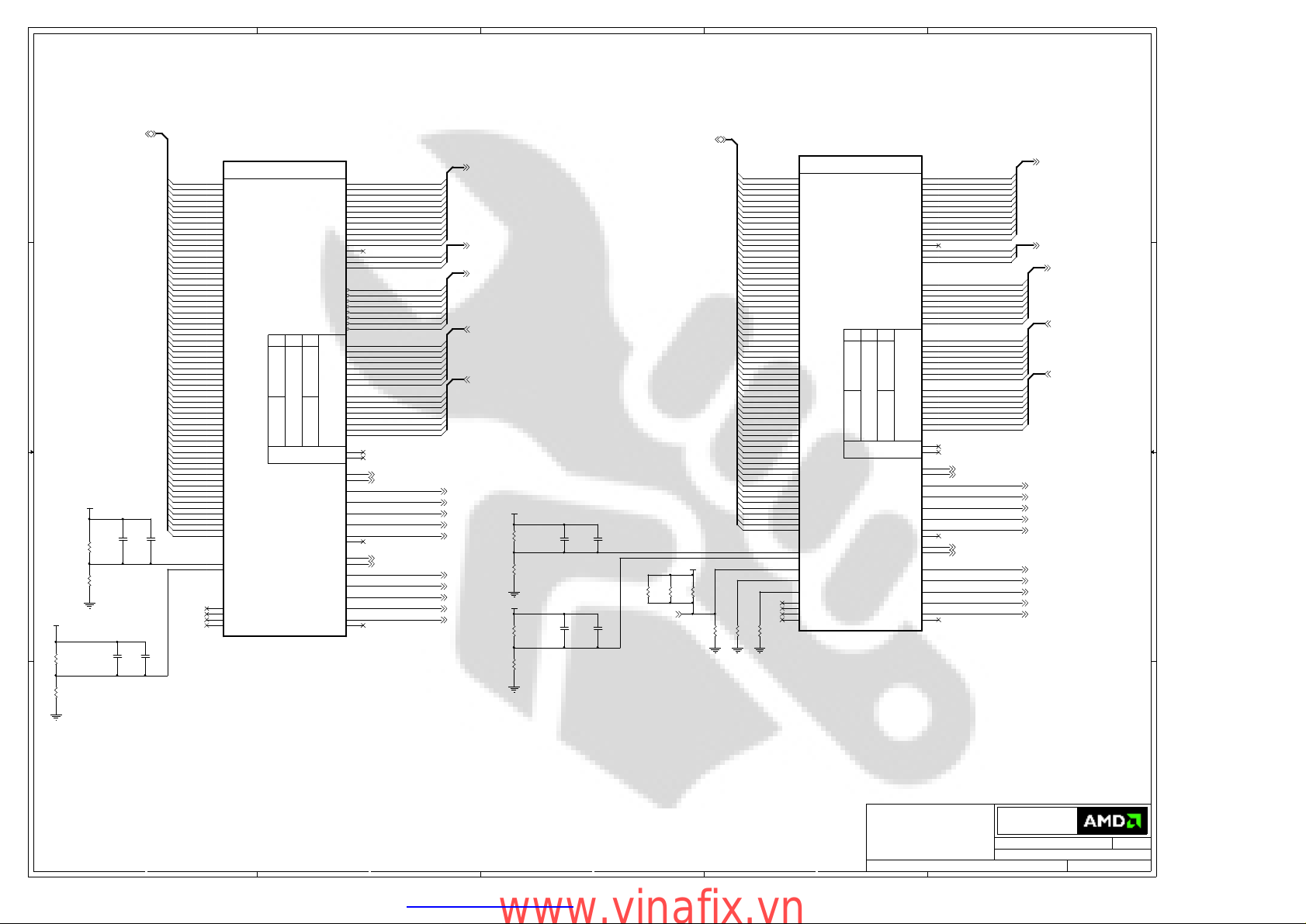
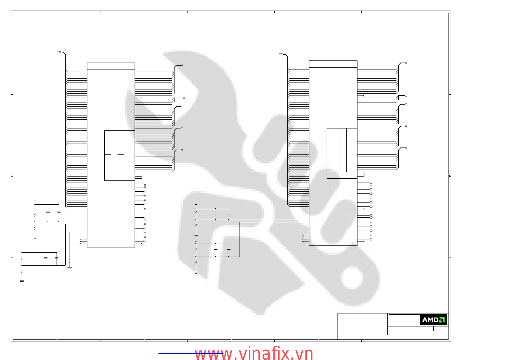
+12V_BUS
C1
CAP CER 10UF 20% 16V X5R
10UF
(1206)1.8MM H MAX
+12V_BUS
+12V_BUS
C3
C2
D D
+3.3V_BUS
+3.3V_BUS
C C
B B
150nF_16V
150nF_16V
LF CAP CER 150NF 10% 16V X7R (0603)
CAP CER 10UF 10% 6.3V X6S
(0805)1.4MM MAX THICK
C4
10uF_X6S
C6
1uF_6.3V
C0
10nF
C5
100nF_6.3V
Place these caps as close to the PCIE
connector as possible
TEST_EN_J TEST_EN_J
No JTAG
R1
0R
PETn0_GFXRn0(2)
PETp1_GFXRp1(2)
PETn1_GFXRn1(2)
PETp2_GFXRp2(2)
PETn2_GFXRn2(2)
PETp3_GFXRp3(2)
PETn3_GFXRn3(2)
PETp4_GFXRp4(2)
PETn4_GFXRn4(2)
PETp5_GFXRp5(2)
PETn5_GFXRn5(2)
PETp6_GFXRp6(2)
PETn6_GFXRn6(2)
PETp7_GFXRp7(2)
PETn7_GFXRn7(2)
PETp8_GFXRp8(2)
PETn8_GFXRn8(2)
PETp9_GFXRp9(2)
PETn9_GFXRn9(2)
PETp10_GFXRp10(2)
PETn10_GFXRn10(2)
PETp11_GFXRp11(2)
PETn11_GFXRn11(2)
PETp12_GFXRp12(2)
PETn12_GFXRn12(2)
PETp13_GFXRp13(2)
PETn13_GFXRn13(2)
PETp14_GFXRp14(2)
PETn14_GFXRn14(2)
PETp15_GFXRp15(2)
PETn15_GFXRn15(2)
PRESENCE
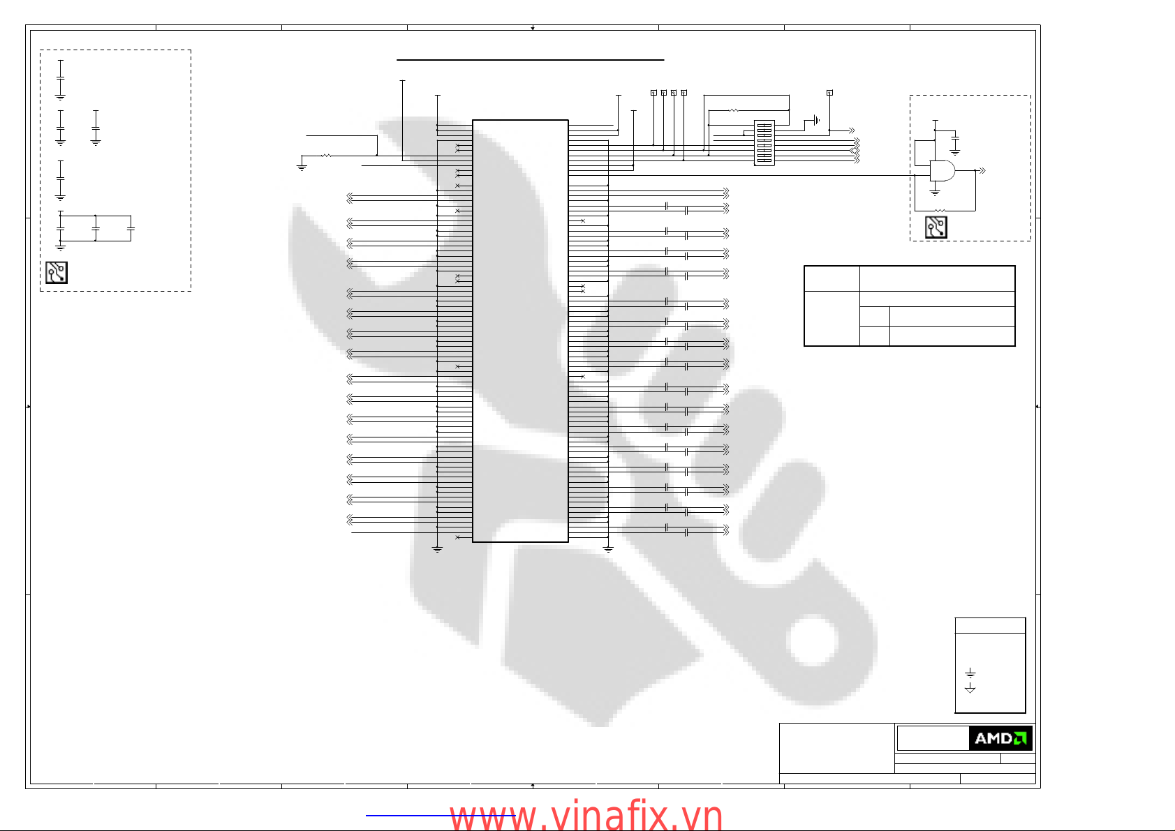
PCI-EXPRESS EDGE CONNECTOR
+3.3V_BUS
+12V_BUS
+12V#B1
+12V#B2
+12V#B3
GND#B4
SMCLK
SMDAT
GND#B7
+3.3V#B8
JTAG1
3.3Vaux
WAKE#
RSVD#B12
GND#B13
PETp0
PETn0
GND#B16
PRSNT2#B17
GND#B18
PETp1
PETn1
GND#B21
GND#B22
PETp2
PETn2
GND#B25
GND#B26
PETp3
PETn3
GND#B29
RSVD#B30
PRSNT2#B31
GND#B32
PETp4
PETn4
GND#B35
GND#B36
PETp5
PETn5
GND#B39
GND#B40
PETp6
PETn6
GND#B43
GND#B44
PETp7
PETn7
GND#B47
PRSNT2#B48
GND#B49
PETp8
PETn8
GND#B52
GND#B53
PETp9
PETn9
GND#B56
GND#B57
PETp10
PETn10
GND#B60
GND#B61
PETp11
PETn11
GND#B64
GND#B65
PETp12
PETn12
GND#B68
GND#B69
PETp13
PETn13
GND#B72
GND#B73
PETp14
PETn14
GND#B76
GND#B77
PETp15
PETn15
GND#B80
PRSNT2#B81
RSVD#B82
x16 PCIe
Mechanical Key
PRSNT1#A1
+12V#A2
+12V#A3
GND#A4
JTAG2
JTAG3
JTAG4
JTAG5
+3.3V#A9
+3.3V#A10
PERST#
GND#A12
REFCLK+
REFCLKGND#A15
PERp0
PERn0
GND#A18
RSVD#A19
GND#A20
PERp1
PERn1
GND#A23
GND#A24
PERp2
PERn2
GND#A27
GND#A28
PERp3
PERn3
GND#A31
RSVD#A32
RSVD#A33
GND#A34
PERp4
PERn4
GND#A37
GND#A38
PERp5
PERn5
GND#A41
GND#A42
PERp6
PERn6
GND#A45
GND#A46
PERp7
PERn7
GND#A49
RSVD#A50
GND#A51
PERp8
PERn8
GND#A54
GND#A55
PERp9
PERn9
GND#A58
GND#A59
PERp10
PERn10
GND#A62
GND#A63
PERp11
PERn11
GND#A66
GND#A67
PERp12
PERn12
GND#A70
GND#A71
PERp13
PERn13
GND#A74
GND#A75
PERp14
PERn14
GND#A78
GND#A79
PERp15
PERn15
GND#A82
MPCIE1
JTRST
B1
B2
B3
B4
B5
B6
B7
B8
B9
B10
B11
B12
B13
B14
B15
B16
B17
B18
B19
B20
B21
B22
B23
B24
B25
B26
B27
B28
B29
B30
B31
B32
B33
B34
B35
B36
B37
B38
B39
B40
B41
B42
B43
B44
B45
B46
B47
B48
B49
B50
B51
B52
B53
B54
B55
B56
B57
B58
B59
B60
B61
B62
B63
B64
B65
B66
B67
B68
B69
B70
B71
B72
B73
B74
B75
B76
B77
B78
B79
B80
B81
B82
A1
A2
A3
A4
A5
A6
A7
A8
A9
A10
A11
A12
A13
A14
A15
A16
A17
A18
A19
A20
A21
A22
A23
A24
A25
A26
A27
A28
A29
A30
A31
A32
A33
A34
A35
A36
A37
A38
A39
A40
A41
A42
A43
A44
A45
A46
A47
A48
A49
A50
A51
A52
A53
A54
A55
A56
A57
A58
A59
A60
A61
A62
A63
A64
A65
A66
A67
A68
A69
A70
A71
A72
A73
A74
A75
A76
A77
A78
A79
A80
A81
A82
PRESENCE
+12V_BUS
JTCK
JTDI
JTDO
JTMS
PERp0
PERn0
PERp1
PERn1
PERp2
PERn2
PERp3
PERn3
PERp4
PERn4
PERp5
PERn5
PERp6
PERn6
PERp7
PERn7
PERp8
PERn8
PERp9
PERn9
PERp10
PERn10
PERp11
PERn11
PERp12
PERn12
PERp13
PERn13
PERp14
PERn14
PERp15
PERn15
+3.3V_BUS
TP4
35mil
100nF_6.3V
100nF_6.3V
100nF_6.3V
100nF_6.3V
100nF_6.3V
100nF_6.3V
100nF_6.3V
100nF_6.3V
100nF_6.3V
100nF_6.3V
100nF_6.3V
100nF_6.3V
100nF_6.3V
100nF_6.3V
100nF_6.3V
100nF_6.3V
TP3
TP1
TP2
35mil
35mil
35mil
No JTAG
R2 0R
TDA08H0SB1R
98
107
TSW1
116
125
134
143
2 1345678
152
ON
161
JTRST
PCIE_REFCLKP (2)
C7
C8
100nF_6.3V
C9
C10
100nF_6.3V
C11
C12
100nF_6.3V
C13
C14
100nF_6.3V
C15
C16
100nF_6.3V
C17
C18
100nF_6.3V
C19
C20
100nF_6.3V
C21
C22
100nF_6.3V
C23
C24
100nF_6.3V
C25
C26
100nF_6.3V
C27
C28
100nF_6.3V
C29
C30
100nF_6.3V
C31
C32
100nF_6.3V
C33
C34
100nF_6.3V
C35
C36
100nF_6.3V
C37
C38
100nF_6.3V
PCIE_REFCLKN (2)PETp0_GFXRp0(2)
GFXTp0_PERp0 (2)
GFXTn0_PERn0 (2)
GFXTp1_PERp1 (2)
GFXTn1_PERn1 (2)
GFXTp2_PERp2 (2)
GFXTn2_PERn2 (2)
GFXTp3_PERp3 (2)
GFXTn3_PERn3 (2)
GFXTp4_PERp4 (2)
GFXTn4_PERn4 (2)
GFXTp5_PERp5 (2)
GFXTn5_PERn5 (2)
GFXTp6_PERp6 (2)
GFXTn6_PERn6 (2)
GFXTp7_PERp7 (2)
GFXTn7_PERn7 (2)
GFXTp8_PERp8 (2)
GFXTn8_PERn8 (2)
GFXTp9_PERp9 (2)
GFXTn9_PERn9 (2)
GFXTp10_PERp10 (2)
GFXTn10_PERn10 (2)
GFXTp11_PERp11 (2)
GFXTn11_PERn11 (2)
GFXTp12_PERp12 (2)
GFXTn12_PERn12 (2)
GFXTp13_PERp13 (2)
GFXTn13_PERn13 (2)
GFXTp14_PERp14 (2)
GFXTn14_PERn14 (2)
GFXTp15_PERp15 (2)
GFXTn15_PERn15 (2)
TP6
35mil
+3.3V
53
1
2
R_RST
R3 0R
C39
100nF_6.3V
NC7SZ08P5X_NL
4
U5
DNI
PERST#_buf (2)
PERST#
TEST_EN_R (3)
HSYNC1 (3,7,15)
VSYNC1 (3,7,15)
DDC1DATA (3,15)
DDC3CLK (3,18)
DDC1CLK (3,15)
Place R3 in U5
Table 1: Connection for JTAG
Production
(No JTAG)
Internal Use Only
TSW1, R1 & R2 are located on the bottom side of the board close to PCIE connector.
Install R1, R2 & Don't Install TSW1
Install TSW1 & Don't Install R1 & R2
TSW1 Switch #1, 2, 3, 4, 5 and 6 closed (ON)
JTAG
#8 and 7 open
TSW1 Switch #1, 2, 3, 4, 5 and 6 open
NO JTAG
#8 & 7 closed (ON)
SYMBOL LEGEND
DO NOT
DNI
INSTALL
ACTIVE
#
LOW
DIGITAL
GROUND
A A
CONFIDENTIAL & PROPRIETARY TO ADVANCED MICRO DEVICES INC.
?2007 Advanced Micro Devices
This AMD Board schematic and design is the exclusive property of AMD,
and is provided only to entities under a non-disclosure agreement
with AMD for evaluation purposes. Further distribution or disclosure
is strictly prohibited. Use of this schematic and design for any purpose
other than evaluation requires a Board Technology License Agreement
with AMD. AMD makes no representations or warranties of any kind
regarding this schematic and design, including, not limited to,
any implied warranty of merchantibility or fitness for a particular
purpose, and disclaims responsibility forany consequences resulting
from use of the information included herein.
Title
8
7
6
5
4
3
RH RV670 - PCI-E Edge Connector
2
Advanced Micro Devices Inc.
1 Commerce Valley Drive East
Markham, Ontario
Friday, September 07, 2007
Sheet
1 21
of
ANALOG
GROUND
BUO BRING UP
ONLY
Doc No.
105-B340xx-00
1
RevDate:
2
PDF created with pdfFactory Pro trial version www.pdffactory.com
www.vinafix.vn
Page 2
5
D D
4
3
2
1
NOTE: some of the PCIE testpoints will
be available trought via on traces.
PETp0_GFXRp0(1)
PETn0_GFXRn0(1)
PETp1_GFXRp1(1)
PETn1_GFXRn1(1)
PETp2_GFXRp2(1)
PETn2_GFXRn2(1)
PETp3_GFXRp3(1)
PETn3_GFXRn3(1)
PETp4_GFXRp4(1)
PETn4_GFXRn4(1)
PETp5_GFXRp5(1)
PETn5_GFXRn5(1)
PETp6_GFXRp6(1)
C C
B B
PCIE_REFCLKP(1)
PCIE_REFCLKN(1)
PETn6_GFXRn6(1)
PETp7_GFXRp7(1)
PETn7_GFXRn7(1)
PETp8_GFXRp8(1)
PETp9_GFXRp9(1)
PETn9_GFXRn9(1)
PETp10_GFXRp10(1)
PETn10_GFXRn10(1)
PETp11_GFXRp11(1)
PETn11_GFXRn11(1)
PETp12_GFXRp12(1)
PETn12_GFXRn12(1)
PETp13_GFXRp13(1)
PETn13_GFXRn13(1)
PETp14_GFXRp14(1)
PETn14_GFXRn14(1)
PETp15_GFXRp15(1)
PETn15_GFXRn15(1)
DNI DNI
R13
R14
51R
51R
402 402
620NOPN008
TP11
620NOPN008
TP12
620NOPN008
TP13
620NOPN008
TP14
620NOPN008
TP19
620NOPN008
TP20
620NOPN008
TP21
620NOPN008
TP22
620NOPN008
TP27
620NOPN008
TP28
620NOPN008
TP7
620NOPN008
TP8
620NOPN008
TP9
620NOPN008
TP10
620NOPN008
TP15
620NOPN008
TP16
620NOPN008
TP17
620NOPN008
TP18
620NOPN008
TP23
620NOPN008
TP24
620NOPN008
TP25
620NOPN008
TP26
PERST#_buf(1)
AW48
AW46
AV51
AV49
AU48
AU46
AT51
AT49
AR48
AR46
AP51
AP49
AN48
AN46
AM51
AM49
AL48
AL46
AK51
AK49
AH51
AH49
AG48
AG46
AF51
AF49
AE48
AE46
AD51
AD49
AW43
AW42
AP36
AJ48
AJ46
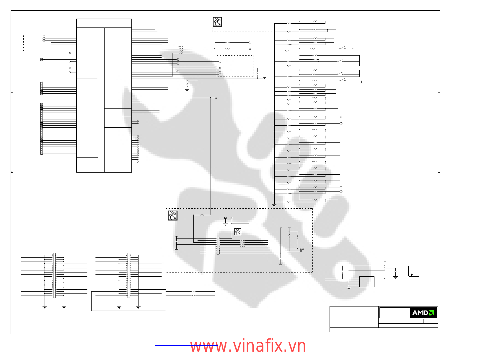
U1A
PCIE_RX0P
PCIE_RX0N
PCIE_RX1P
PCIE_RX1N
PCIE_RX2P
PCIE_RX2N
PCIE_RX3P
PCIE_RX3N
PCIE_RX4P
PCIE_RX4N
PCIE_RX5P
PCIE_RX5N
PCIE_RX6P
PCIE_RX6N
PCIE_RX7P
PCIE_RX7N
PCIE_RX8P
PCIE_RX8N
PCIE_RX9P
PCIE_RX9N
PCIE_RX10P
PCIE_RX10N
PCIE_RX11P
PCIE_RX11N
PCIE_RX12P
PCIE_RX12N
PCIE_RX13P
PCIE_RX13N
PCIE_RX14P
PCIE_RX14N
PCIE_RX15P
PCIE_RX15N
Clock
PCIE_REFCLKP
PCIE_REFCLKN
PERSTB
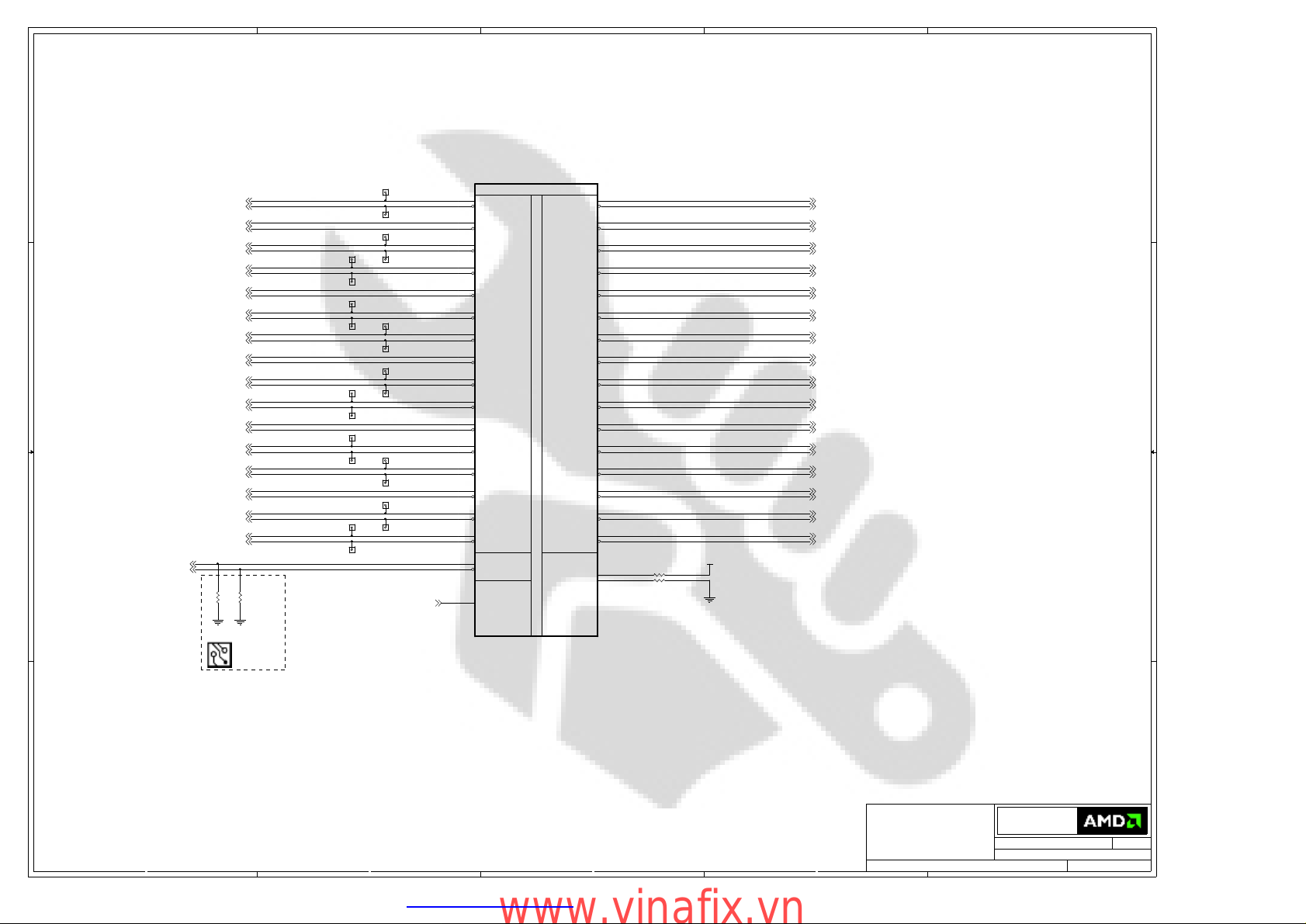
PART 1 OF 10
P
C
I
E
X
P
R
E
S
S
I
N
T
E
R
F
A
C
E
PCIE_TX0P
PCIE_TX0N
PCIE_TX1P
PCIE_TX1N
PCIE_TX2P
PCIE_TX2N
PCIE_TX3P
PCIE_TX3N
PCIE_TX4P
PCIE_TX4N
PCIE_TX5P
PCIE_TX5N
PCIE_TX6P
PCIE_TX6N
PCIE_TX7P
PCIE_TX7N
PCIE_TX8P
PCIE_TX8N
PCIE_TX9P
PCIE_TX9N
PCIE_TX10P
PCIE_TX10N
PCIE_TX11P
PCIE_TX11N
PCIE_TX12P
PCIE_TX12N
PCIE_TX13P
PCIE_TX13N
PCIE_TX14P
PCIE_TX14N
PCIE_TX15P
PCIE_TX15N
Calibration
PCIE_CALRN
PCIE_CALRP
AU40
AU39
AU43
AU42
AT40
AT39
AT43
AT42
AP40
AP39
AP43
AP42
AN40
AN39
AN43
AN42
AL40
AL39
AL43
AL42
AK40
AK39
AK43
AK42
AH40
AH39
AH43
AH42
AG40
AG39
AG43
AG42
AN37
AP37
GFXTp0_PERp0 (1)
GFXTn0_PERn0 (1)
GFXTp1_PERp1 (1)
GFXTn1_PERn1 (1)
GFXTp2_PERp2 (1)
GFXTn2_PERn2 (1)
GFXTp3_PERp3 (1)
GFXTn3_PERn3 (1)
GFXTp4_PERp4 (1)
GFXTn4_PERn4 (1)
GFXTp5_PERp5 (1)
GFXTn5_PERn5 (1)
GFXTp6_PERp6 (1)
GFXTn6_PERn6 (1)
GFXTp7_PERp7 (1)
GFXTn7_PERn7 (1)
GFXTp8_PERp8 (1)
GFXTn8_PERn8 (1)PETn8_GFXRn8(1)
GFXTp9_PERp9 (1)
GFXTn9_PERn9 (1)
GFXTp10_PERp10 (1)
GFXTn10_PERn10 (1)
GFXTp11_PERp11 (1)
GFXTn11_PERn11 (1)
GFXTp12_PERp12 (1)
GFXTn12_PERn12 (1)
GFXTp13_PERp13 (1)
GFXTn13_PERn13 (1)
GFXTp14_PERp14 (1)
GFXTn14_PERn14 (1)
GFXTp15_PERp15 (1)
GFXTn15_PERn15 (1)
+PCIE_VDDC
402
R82.0K
402
R91.27K
For Tektronix LA only
Place close
to ASIC
A A
5
4
RV670 PRO
CONFIDENTIAL & PROPRIETARY TO ADVANCED MICRO DEVICES INC.
?2007 Advanced Micro Devices
This AMD Board schematic and design is the exclusive property of AMD,
and is provided only to entities under a non-disclosure agreement
with AMD for evaluation purposes. Further distribution or disclosure
is strictly prohibited. Use of this schematic and design for any purpose
other than evaluation requires a Board Technology License Agreement
with AMD. AMD makes no representations or warranties of any kind
regarding this schematic and design, including, not limited to,
any implied warranty of merchantibility or fitness for a particular
purpose, and disclaims responsibility forany consequences resulting
from use of the information included herein.
Title
3
2
RH RV670 - ASIC PCIE_Interface
Advanced Micro Devices Inc.
1 Commerce Valley Drive East
Markham, Ontario
Friday, September 07, 2007
Sheet
2 21
of
1
Doc No.
RevDate:
2
105-B340xx-00
PDF created with pdfFactory Pro trial version www.pdffactory.com
www.vinafix.vn
Page 3
5
Recommended caps:
(see BOM for qualified values/vendors)
10uF , X6S, 0805, 6.3V, 1.4MM MAX THICK
4.7uF , X6S/X5R, 0603, 6.3V
1uF, X6S, 0402, 6.3V
100nF, X7R, 0402
10nF , X7R, 0402
Place close to ASIC
NS100
NS_VIA
1 2
GND_T2PVSS
10uF_X6S
DDC3DATA(18)
DDC3CLK(1,18)
3
1
R106 100R
R100 100R
R101 100R
R102 100R
R103 100R
R104 100R
R105 100R
10uF_X6S
C103
R7
1K
OSC_EN
DNI
C100
1uF_6.3V
C106
1uF_6.3V
+3.3V
R40
4.7K
402 402
+1.8V
R43 221R
R44 110R
C46 100nF_6.3V
DNI
NR81 182R
R81 182R
Share one pad
C102
C108
1uF_6.3V
R41
4.7K
TP42
OSC_EN (14)
T2XCM
T2XCP
T2X0M
T2X0P
T2X1M
T2X1P
T2X2M
T2X2P
T2X3M
T2X3P
T2X4M
T2X4P
T2X5M
T2X5P
C101
100nF_6.3V
C109
100nF_6.3V
DDC1DATA(1,15)
DDC2DATA(16)
DDC4DATA
DDC4CLK
GPU_DMINUS(18)
GPU_DPLUS(18)
TS_FDO(18)
D D
+1.8V
B102
BLM15BD121SN1
Q100
SI2304DS
1
+3.3V
TR40
4.7K
402 402
BUO BUO
I2C DEVICE ADDRESS
DEVICE
LM63
ADS1112
XTALOUT_S
C80
100nF_6.3V
32
TR41
4.7K
XTALOUT_S
is done for
ease of layout
C C
LVT_EN(13)
DDC4DATA(13)
DDC4CLK(13)
B B
TEST_EN_R(1)
+3.3V_BUS
B80
BLM15BD121SN1
C81
1uF_6.3V
A A
T2XCM(15)
T2XCP(15)
T2X0M(15)
T2X0P(15)
T2X1M(15)
T2X1P(15)
T2X2M(15)
T2X2P(15)
T2X3M(15)
T2X3P(15)
T2X4M(15)
T2X4P(15)
T2X5M(15)
T2X5P(15)
+T2PVDD
+T2XVDD
B100
26R_600mA
Use 0R
TP41
TP40
ADDRESS
1001 100 (R/W#) --> DDC3
1001 000 (R/W#) --> DDC4 BUO
TR7 0R
DNI
Y81
4
VCC
OUT
2
GND
E/D
27.000MHz
DDC1CLK(1,15)
DDC2CLK(16)
DDC3DATA
DDC3CLK
HPD1(16)
SDA(7)
SCL(7)
PLL_TEST
TEST_EN
4
U1B
Integrated TMDS2
BH35
T2XCM
BF35
T2XCP
BL36
T2X0M
BJ36
T2X0P
BH37
T2X1M
BF37
T2X1P
BL38
T2X2M
BJ38
T2X2P
BH39
T2X3M
BF39
T2X3P
BH41
T2X4M
BF41
T2X4P
BL42
T2X5M
BJ42
T2X5P
BL44
TXOUT_U2N
BJ44
TXOUT_U2P
BL46
TXOUT_U3N
BJ46 BJ30
TXOUT_U3P TXCBP
BJ40
TXCLK_UP
BL40
TXCLK_UN
BE38
LPVDD
BE40
LPVSS
BG34
LVDDC1
BK35
LVDDC2
BL34
LVDDR1
BJ34
LVDDR2
BE36
LVSSR1
BE42
LVSSR2
BL49
LVSSR3
BG36
LVSSR4
BG38
LVSSR5
BG40
LVSSR6
BG42
LVSSR7
BF44
LVSSR8
BK37
LVSSR9
BK39
LVSSR10
BK41
LVSSR11
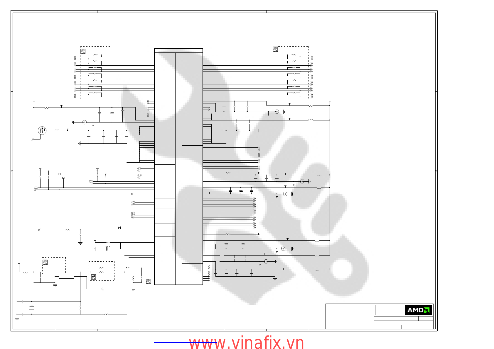
Monitor Interface
BB45
DDC1DATA
BB47
DDC1CLK
AV36
DDC2DATA
AW36
DDC2CLK
AU32
DDC3DATA
AT32
DDC3CLK
AV35
DDC4DATA
AW35
DDC4CLK
BB29
HPD1
AV27
SDA
SCL
DMINUS
DPLUS
TS_FDO
PLLTEST
TESTEN
VREFG
XTALIN
XTALOUT
RV670 PRO
MMI2C
Thermal
Diode
Test
XTALIN
XTALOUT
VREFG
R82
221R
Share one pad
DNI
MR82
221R
AV29
BC27
BB27
AT21
AU36
AT37
AT20
BF46
BJ49
PART 2 OF 10
V
I
D
E
O
&
M
U
L
T
I
M
E
D
I
A
Integrated TMDS
TXVDDR1
TXVDDR2
TXVDDR3
TXVDDR4
TXVSSR1
TXVSSR2
TXVSSR3
TXVSSR4
TXVSSR5
TXVSSR6
TXVSSR7
TXVSSR8
TXVSSR9
TXVSSR10
DAC / CRT
DAC2 (TV/CRT2)
H2SYNC
V2SYNC
A2VDDQ
A2VSSQ
TXCAM
TXCAP
TX0M
TX0P
TX1M
TX1P
TX2M
TX2P
TX3M
TX3P
TX4M
TX4P
TX5M
TX5P
TPVDD
TPVSS
TXCBM
HSYNC
VSYNC
RSET
AVDD
AVSSQ
VDD1DI
VSS1DI
COMP
R2SET
VDD2DI
VSS2DI
A2VDD
NC_1
NC_2
NC_3
NC_4
NC_5
NC_6
NC_7
BL26
BJ26
BH27
BF27
BL28
BJ28
BH29
BF29
BH31
BF31
BL32
BJ32
BH33
BF33
BL24
BJ24
BL30
BE26
BF25
BH25
BK25
BE28
BE30
BG26
BG28
BG30
BG32
BK27
BK29
BK31
BK33
BB49
R
BB51
RB
BD49
G
BD51
GB
BF49
B
BF51
BB
BA42
BA43
BB43
BD46
BD44
BA50
BA48
BA39
R2
AY39
R2B
BC39
G2
BB39
G2B
BC37
B2
BB37
B2B
BA36
AY36
AY37
Y
BA37
C
AW37
R2SET GND_A2VSSQ
BA40
BC42
BB41
BC36
BB36
BC41
BC40
BB40
BB32
BE34
BC33
BC32
BE32
3
R1030 499R
R2030 715R
C2030
10nF
C111
100nF_6.3V
C115
100nF_6.3V
C2021
100nF_6.3V
C2024
10nF
C2031
100nF_6.3V
C1023
10nF
T1XCM
T1XCP
T1X0M
T1X0P
T1X1M
T1X1P
T1X2M
T1X2P
T1X3M
T1X3P
T1X4M
T1X4P
T1X5M
T1X5P
C112
1uF_6.3V
C116
1uF_6.3V
GND_AVSSQRSET
DNI
C2025
100nF_6.3V
C2032
1uF_6.3V
C113
10uF_X6S
C1024
100nF_6.3V
C2022
1uF_6.3V
C2026
1uF_6.3V
GND_VSS2DI
C117
10uF_X6S
C1020
10nF
C1025
1uF_6.3V
A_DAC2_R (16)
A_DAC2_RB (16)
A_DAC2_G (16)
A_DAC2_GB (16)
A_DAC2_B (16)
A_DAC2_BB (16)
HSYNC2 (7,16)
VSYNC2 (7,16)
A_DAC2_Y (17)
A_DAC2_C (17)
A_DAC2_COMP (17)
NS2021 NS_VIA
C2033
4.7uF_6.3V
GND_TPVSS
A_DAC1_R (15)
A_DAC1_RB (15)
A_DAC1_G (15)
A_DAC1_GB (15)
A_DAC1_B (15)
A_DAC1_BB (15)
HSYNC1 (1,7,15)
VSYNC1 (1,7,15)
GND_AVSSQ
C1021
100nF_6.3V
GND_A2VSSQ
NS2020 NS_VIA
+VDD2DI
12
Place close to ASIC
DNI
R116 182R
R110 182R
R111 182R
R112 182R
R113 182R
R114 182R
R115 182R
+TPVDD
NS110
NS_VIA
12
+TXVDDR
+AVDD
C1022
1uF_6.3V
+VDD1DI
NS1021NS_VIA
GND_VSS1DI
+A2VDDQ
12
GND_A2VSSQ
+A2VDD
NS1020 NS_VIA
GND_AVSSQ
12
2
T1XCM (16)
T1XCP (16)
T1X0M (16)
T1X0P (16)
T1X1M (16)
T1X1P (16)
T1X2M (16)
T1X2P (16)
T1X3M (16)
T1X3P (16)
T1X4M (16)
T1X4P (16)
T1X5M (16)
T1X5P (16)
B112
BLM15BD121SN1
B110
26R_600mA
B1020
BLM15BD121SN1
12
BLM15BD121SN1
B2020
BLM15BD121SN1
B2021
BLM15BD121SN1
B2030
BLM15BD121SN1
1
+1.8V
B1021
+3.3V
C82
12pF_50V
C83
12pF_50V
2 1
Y82
27.000MHz_10PPM
XTALIN_S
R84
XTALOUT_S
1M
MR86 0R
For Crystal: Adjust C82, C83, R81
5
XTALOUT
4
PDF created with pdfFactory Pro trial version www.pdffactory.com
www.vinafix.vn
CONFIDENTIAL & PROPRIETARY TO ADVANCED MICRO DEVICES INC.
?2007 Advanced Micro Devices
This AMD Board schematic and design is the exclusive property of AMD,
and is provided only to entities under a non-disclosure agreement
with AMD for evaluation purposes. Further distribution or disclosure
is strictly prohibited. Use of this schematic and design for any purpose
other than evaluation requires a Board Technology License Agreement
with AMD. AMD makes no representations or warranties of any kind
regarding this schematic and design, including, not limited to,
any implied warranty of merchantibility or fitness for a particular
purpose, and disclaims responsibility forany consequences resulting
from use of the information included herein.
Title
3
2
RH RV670 - ASIC MAIN
Advanced Micro Devices Inc.
1 Commerce Valley Drive East
Markham, Ontario
Friday, September 07, 2007
Sheet
3 21
of
1
Doc No.
RevDate:
2
105-B340xx-00
Page 4
C151
1uF_6.3V
C133
1uF_6.3V
C141
1uF_6.3V
C981
1uF_6.3V
C961
1uF_6.3V
C972
100nF_6.3V
MC955
4.7uF_6.3V
C955
10uF_X6S
BLM15BD121SN1
B94
BLM15BD121SN1
B69
BLM15BD121SN1
NS70NS_VIA
1 2
GND_PVSS
B60
BLM15BD121SN1
5
C152
1uF_6.3V
C135
1uF_6.3V
C142
1uF_6.3V
C982
1uF_6.3V
C962
1uF_6.3V
C973
100nF_6.3V
C956
10uF_X6S
C121
1uF_6.3V
Use 0R
MB67
220R_2A
B67
220R_2A
NS64NS_VIA
1 2
GND_MPVSS
5
C153
1uF_6.3V
C143
1uF_6.3V
C963
1uF_6.3V
MC956
4.7uF_6.3V
C958
10uF_X6S
NS122 NS_VIA
1 2
GND_VSSRHC
+DPLL_PVDD
DNI
GND_MPVSS
GND_MPVSS
C136
1uF_6.3V
C983
1uF_6.3V
C964
1uF_6.3V
C974
100nF_6.3V
+3.3V
+DPLL_VDDC
GND_PVSS
C155
C156
C154
1uF_6.3V
1uF_6.3V
C138
C139
1uF_6.3V
1uF_6.3V
C145
C144
1uF_6.3V
MC958
4.7uF_6.3V
C959
10uF_X6S
+MPVDD
C146
1uF_6.3V
1uF_6.3V
C984
C985
1uF_6.3V
1uF_6.3V
C965
C966
1uF_6.3V
1uF_6.3V
C130
100nF_6.3V
MC959
4.7uF_6.3V C940
C126
10uF_X6S
NS123NS_VIA
1 2
GND_VSSRHD
C91
100nF_6.3V
+VDDR_DVP
C94
10uF_X6S
C60
C68
10uF_X6S
1uF_6.3V
C62
10uF_X6S
C67
10uF_X6S
1uF_6.3V
C975
1uF_6.3V
C147
1uF_6.3V
C986
1uF_6.3V
C967
1uF_6.3V
C134
C131
100nF_6.3V
100nF_6.3V
MC126
4.7uF_6.3V
C127
10uF_X6S
C120
1uF_6.3V
NS120 NS_VIA
1 2
GND_VSSRHA
C122
1uF_6.3V
C123
1uF_6.3V
C92
100nF_6.3V
C69
100nF_6.3V
C64
C61
10nF
100nF_6.3V
C66
1uF_6.3V
C157
1uF_6.3V
C976
1uF_6.3V
C148
1uF_6.3V
C987
1uF_6.3V
C968
1uF_6.3V
MC127
4.7uF_6.3V
Overlapped Footprints
C128
10uF_X6S
C93
100nF_6.3V
C95
1uF_6.3V
+DPLL_PVDD
GND_PVSS
C63
1uF_6.3V
C65
100nF_6.3V
+MVDD
C150
1uF_6.3V
C132
1uF_6.3V
D D
C C
B B
A A
C140
1uF_6.3V
C980
1uF_6.3V
C960
1uF_6.3V
C971
100nF_6.3V
MC954
4.7uF_6.3V
10uF_X6S
+MVDD
B120
B121
BLM15BD121SN1
NS121 NS_VIA
1 2
GND_VSSRHB
B122
BLM15BD121SN1
B123
BLM15BD121SN1
+1.8V
+1.1V
+VDDCI_LDO
+VDDC
Recommended caps:
(see BOM for qualified values/vendors)
10uF , X6S, 0805, 6.3V, 1.4MM MAX THICK
4.7uF , X6S/X5R, 0603, 6.3V
1uF, X6S, 0402, 6.3V
100nF, X7R, 0402
10nF , X7R, 0402
C158
1uF_6.3V
C977
1uF_6.3V
C149
1uF_6.3V
C988
1uF_6.3V
C969
1uF_6.3V
C137
100nF_6.3V
MC128
4.7uF_6.3V
C97
100nF_6.3V
+DPLL_VDDC
+MPVDD
C159
1uF_6.3V
C989
1uF_6.3V
+VDDRHA
+VDDRHB
C96
1uF_6.3V
4
C978
1uF_6.3V
C979
1uF_6.3V
C970
1uF_6.3V
+VDDRHC
+VDDRHD
4
C98
100nF_6.3V
AD15
AA14
AB45
AA40
AD43
AC37
AB10
AE13
AH11
AF15
AL13
AP12
BC14
AU11
BA10
AW14
AT15
AM12
AM11
AT26
AT27
AT29
AT30
BF23
BH23
BK23
BE22
BG22
BA35
BB35
BC35
W15
W12
W11
BJ22
W20
W19
G14
G18
G22
G26
G30
R34
G40
T15
M26
P29
L38
M39
L10
N19
M32
N16
P25
K35
T19
R22
K43
P41
P45
T12
V38
U40
V45
AB7
AF7
AK7
AP7
AV7
V42
V41
L31
L29
T22
T23
Y19
P7
V7
U1G
VDDR1#1
VDDR1#2
VDDR1#3
VDDR1#4
VDDR1#5
VDDR1#6
VDDR1#7
VDDR1#8
VDDR1#9
VDDR1#10
VDDR1#11
VDDR1#12
VDDR1#13
VDDR1#14
VDDR1#15
VDDR1#16
VDDR1#17
VDDR1#18
VDDR1#19
VDDR1#20
VDDR1#21
VDDR1#22
VDDR1#23
VDDR1#24
VDDR1#25
VDDR1#26
VDDR1#27
VDDR1#28
VDDR1#29
VDDR1#30
VDDR1#31
VDDR1#32
VDDR1#33
VDDR1#34
VDDR1#35
VDDR1#36
VDDR1#37
VDDR1#38
VDDR1#39
VDDR1#40
VDDR1#41
VDDR1#42
VDDR1#43
VDDR1#44
VDDR1#45
VDDR1#46
VDDR1#47
VDDR1#48
VDDR1#49
VDDR1#50
VDDR1#51
VDDR1#52
VDDRHA
VSSRHA
VDDRHB
VSSRHB
VDDRHC
VSSRHC
VDDRHD
VSSRHD
VDDR3#1
VDDR3#2
VDDR3#3
VDDR3#4
VDDR4#1
VDDR4#2
VDDR4#3
VDDR5#1
VDDR5#2
VDDR5#3
DPLL_PVDD
DPLL_PVSS
DPLL_VDDC
MPVDD
MPVSS
NC_15
NC_16
NC_17
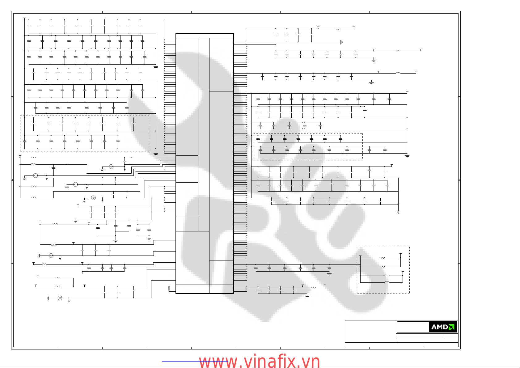
RV670 PRO
Part 7 OF 10
Memory I/O
3
C931
C930
C900
1uF_6.3V
C161
1uF_6.3V
C171
1uF_6.3V
1uF_6.3V
C1125
10uF_X6S
MC1125
4.7uF_6.3V
C1102
1uF_6.3V
C1111
1uF_6.3V
C78
100nF_6.3V
C162
1uF_6.3V
C172
1uF_6.3V
C941
1uF_6.3V
C1136
10uF_X6S
MC1136
4.7uF_6.3V
C1103
1uF_6.3V
C1112
1uF_6.3V
C1123
100nF_6.3V
C913
1uF_6.3V
C79
100nF_6.3V
10nF
C920
1uF_6.3V
C901
100nF_6.3V
AY51
PCIE_PVDD
AF36
PCIE_VDDC1
AF37
PCIE_VDDC2
AG36
PCIE_VDDC3
AG37
PCIE_VDDC4
AH36
PCIE_VDDC5
AH37
PCIE_VDDC6
AK36
PCIE_VDDC7
AK37
PCIE_VDDC8
AL36
PCIE_VDDC9
AL37
PCIE_VDDC10
AN36
PCIE_VDDC11
AF38
PCIE_VDDC12
AW40
PCIE_VDDR1
AW41
PCIE_VDDR2
AY41
PCIE_VDDR3
AY42
PCIE_VDDR4
PCI -Ex press
P
O
W
E
R
Core
PCIE_VDDR5
PCIE_VDDR6
PCIE_VDDR7
PCIE_VDDR8
VDDC0
VDDC1
VDDC2
VDDC3
VDDC4
VDDC5
VDDC6
VDDC7
VDDC8
VDDC9
VDDC10
VDDC11
VDDC12
VDDC13
VDDC14
VDDC15
VDDC16
VDDC17
VDDC18
VDDC19
VDDC20
VDDC21
VDDC22
VDDC23
VDDC24
VDDC25
VDDC26
VDDC27
VDDC28
VDDC29
VDDC30
VDDC31
VDDC32
VDDC33
VDDC34
VDDC35
VDDC36
VDDC37
VDDC38
VDDC39
VDDC40
VDDC41
VDDC42
VDDC43
VDDC44
VDDC45
VDDC46
VDDC47
VDDC48
VDDC49
VDDC50
VDDC51
VDDC52
VDDC53
VDDC54
VDDC55
VDDC56
VDDC57
VDDC58
VDDC59
VDDC60
VDDC61
VDDC62
VDDC63
VDDC64
VDDC65
VDDC66
VDDC67
VDDC68
VDDC69
VDDC70
VDDC71
VDDC72
VDDC73
VDDC74
VDDCI1
VDDCI2
VDDCI3
VDDCI4
VDDCI5
VDDCI6
VDDCI7
VDDCI8
VDD_CT1
VDD_CT2
VDD_CT3
AY43
AY45
AY47
BA46
AM19
W26
W28
W31
W33
Y25
Y27
Y30
Y32
AA24
AA26
AA28
AA31
AA33
AB22
AB25
AB27
AB30
AB32
AD21
AD24
AD26
AD28
AD31
AD33
AE20
AE22
AE25
AE27
AE30
AE32
AF19
AF21
AF24
AF26
AF28
AF31
AF33
AG20
AG22
AG25
AG27
AG30
AG32
AH19
AH21
AH24
AH26
AH28
AH31
AH33
AK20
AK22
AK25
AK27
AK30
AK32
AL19
AL21
AL24
AL26
AL28
AL31
AL33
AM22
AM25
AM27
AM30
AM32
AN21
AN24
AN26
AN28
AN31
AN33
W21
W24
Y20
Y22
AA19
AA21
AB20
AD19
BG14
BJ14
BL14
C911
1uF_6.3V
3
C163
1uF_6.3V
C173
1uF_6.3V
C1104
1uF_6.3V
C1114
1uF_6.3V
C77
1uF_6.3V
100nF_6.3V
C921
1uF_6.3V
C902
1uF_6.3V
C946
1uF_6.3V
C1137
10uF_X6SC954
MC1137
4.7uF_6.3V
C180
100nF_6.3V
C914
100nF_6.3V
C164
1uF_6.3V
C174
1uF_6.3V
C1115
1uF_6.3V
C932
10uF_X6S
C922
1uF_6.3V
C903
1uF_6.3V
C165
1uF_6.3V
C175
1uF_6.3V
C1138
10uF_X6S
MC1138
4.7uF_6.3V
Overlapped Footprints
C1107
1uF_6.3V
C1116
1uF_6.3V
C942
100nF_6.3V
C915
100nF_6.3V
+VDD_CT
C76
1uF_6.3V
+PCIE_PVDD
C933
1uF_6.3V
C923
1uF_6.3V
C904
100nF_6.3V
C166
1uF_6.3V
C176
1uF_6.3V
C948
1uF_6.3V
C1139
10uF_X6S
MC1139
4.7uF_6.3V
C1100
1uF_6.3V
C1117
1uF_6.3V
C1113
100nF_6.3V
C918
4.7uF_6.3V
B76
BLM15BD121SN1
+1.8V
2
C949
1uF_6.3V
C1121
1uF_6.3V
2
C924
1uF_6.3V
C905
1uF_6.3V
C167
1uF_6.3V
C177
1uF_6.3V
C182
10uF_X6S
MC182
4.7uF_6.3V
C947
100nF_6.3V
C919
10uF_X6S
B930
+1.8V
BLM15BD121SN1
C925
C926
1uF_6.3V
10uF_X6S
C907
C906
4.7uF_6.3V
1uF_6.3V
C168
C169
C183
10uF_X6S
1uF_6.3V
C186
1uF_6.3V
MC183
4.7uF_6.3V
C1127
1uF_6.3V
C1130
1uF_6.3V
C178
100nF_6.3V
+VDDCI
C170
1uF_6.3V
C1133
1uF_6.3V
C185
1uF_6.3V
C1131
100nF_6.3V
C1110
1uF_6.3V
1uF_6.3V
C179
1uF_6.3V
C1122
1uF_6.3V
See BOM for qualified option
CONFIDENTIAL & PROPRIETARY TO ADVANCED MICRO DEVICES INC.
?2007 Advanced Micro Devices
This AMD Board schematic and design is the exclusive property of AMD,
and is provided only to entities under a non-disclosure agreement
with AMD for evaluation purposes. Further distribution or disclosure
is strictly prohibited. Use of this schematic and design for any purpose
other than evaluation requires a Board Technology License Agreement
with AMD. AMD makes no representations or warranties of any kind
regarding this schematic and design, including, not limited to,
any implied warranty of merchantibility or fitness for a particular
purpose, and disclaims responsibility forany consequences resulting
from use of the information included herein.
Title
RH RV670 - ASIC Power
+PCIE_VDDC
+PCIE_VDDR
C160
1uF_6.3V
MC187
4.7uF_6.3V
C1128
1uF_6.3V
C1132
1uF_6.3V
B920 220R_2A
26R_600mA
C184
1uF_6.3V
MC181
4.7uF_6.3V
+VDDC
C1129
1uF_6.3V
C1134
1uF_6.3V
C943
100nF_6.3V
+VDDCI_LDO
MR910
0R
MR911
0R
B911 220R_2A
B910 220R_2A
1
+1.8V
B900
+VDDC
+VDDC
Advanced Micro Devices Inc.
1 Commerce Valley Drive East
Markham, Ontario
Friday, September 07, 2007
Sheet
4 21
of
1
+1.1V
Doc No.
RevDate:
2
105-B340xx-00
PDF created with pdfFactory Pro trial version www.pdffactory.com
www.vinafix.vn
Page 5
5
4
3
2
1
+MVDD
40.2R
402
1%
R292
100R
402
1%
DQA_[63..0](9)
C291
100nF_6.3VR291
C293
100nF_6.3V
C294
10nF
C292
10nF
DQA_0
DQA_1
DQA_2
DQA_3
DQA_4
DQA_5
DQA_6
DQA_7
DQA_8
DQA_9
DQA_10
DQA_11
DQA_12
DQA_13
DQA_14
DQA_15
DQA_16
DQA_17
DQA_18
DQA_19
DQA_20
DQA_21
DQA_22
DQA_23
DQA_24
DQA_25
DQA_26
DQA_27
DQA_28
DQA_29
DQA_30
DQA_31
DQA_32
DQA_33
DQA_34
DQA_35
DQA_36
DQA_37
DQA_38
DQA_39
DQA_40
DQA_41
DQA_42
DQA_43
DQA_44
DQA_45
DQA_46
DQA_47
DQA_48
DQA_49
DQA_50
DQA_51
DQA_52
DQA_53
DQA_54
DQA_55
DQA_56
DQA_57
DQA_58
DQA_59
DQA_60
DQA_61
DQA_62
DQA_63
MVREFD_A
MVREFS_A
AD38
AD39
AD40
AD41
AC39
AC46
AC43
AD37
AC36
AB47
AB49
AB51
AA46
AA42
W48
W46
R48
R46
M47
K51
K49
L48
K47
K45
H46
H49
H51
A46
C49
C46
U42
R41
R42
R43
L42
K42
N41
F44
E42
C42
A44
A40
C40
E40
F39
B39
C38
A38
E38
C36
B35
F35
A36
U36
V40
Y51
V47
V49
V51
U46
U50
P49
P47
Y43
Y42
P51
N50
N46
J43
J40
U1C
DQA_0
DQA_1
DQA_2
DQA_3
DQA_4
DQA_5
DQA_6
DQA_7
DQA_8
DQA_9
DQA_10
DQA_11
DQA_12
DQA_13
DQA_14
DQA_15
DQA_16
DQA_17
DQA_18
DQA_19
DQA_20
DQA_21
DQA_22
DQA_23
DQA_24
DQA_25
DQA_26
DQA_27
DQA_28
DQA_29
DQA_30
DQA_31
DQA_32
DQA_33
DQA_34
DQA_35
DQA_36
DQA_37
DQA_38
DQA_39
DQA_40
DQA_41
DQA_42
DQA_43
DQA_44
DQA_45
DQA_46
DQA_47
DQA_48
DQA_49
DQA_50
DQA_51
DQA_52
DQA_53
DQA_54
DQA_55
DQA_56
DQA_57
DQA_58
DQA_59
DQA_60
DQA_61
DQA_62
DQA_63
MVREFDA
MVREFSA
NC_8
NC_9
NC_31
NC_32
RV670 PRO
Part 3 of 10
MEMORY INTERFA C E
A
DDR1 DDR2 DDR3
bidir. strobe
bidir. differenti al stro be
Not used
For DDR2
read strobe
wri te s trobe
MAA_0
MAA_1
MAA_2
MAA_3
MAA_4
MAA_5
MAA_6
MAA_7
MAA_8
MAA_9
MAA_10
MAA_11
MAA_12
MAA_13
MAA_14
MAA_15
DQMAB_0
DQMAB_1
DQMAB_2
DQMAB_3
DQMAB_4
DQMAB_5
DQMAB_6
DQMAB_7
QSA_0
QSA_1
QSA_2
QSA_3
QSA_4
QSA_5
QSA_6
QSA_7
QSA_0B
QSA_1B
QSA_2B
QSA_3B
QSA_4B
QSA_5B
QSA_6B
QSA_7B
ODTA0
ODTA1
CLKA0
CLKA0B
CKEA0
RASA0B
CASA0B
WEA0B
CSA0B_0
CSA0B_1
CLKA1
CLKA1B
CKEA1
RASA1B
CASA1B
WEA1B
CSA1B_0
CSA1B_1
U38
U39
R37
Y38
AA37
Y37
Y39
Y40
K39
K38
M38
M37
P38
P39
L40
K40
Y49
T47
AC42
M49
F49
P43
F41
D37
AA50
T51
AC41
L46
C51
N43
A42
E36
Y47
T49
AA43
M51
F46
N42
D41
F37
V37
AA41
V43
U43
R38
P37
R40
Y36
AA38
V36
G38
J39
L37
J37
J35
N37
P40
K37
MAA_0
MAA_1
MAA_2
MAA_3
MAA_4
MAA_5
MAA_6
MAA_7
MAA_8
MAA_9
MAA_10
MAA_11
MAA_BA2
MAA_BA0
MAA_BA1
DQMAb_0
DQMAb_1
DQMAb_2
DQMAb_3
DQMAb_4
DQMAb_5
DQMAb_6
DQMAb_7
QSA_0
QSA_1
QSA_2
QSA_3
QSA_4
QSA_5
QSA_6
QSA_7
QSAb_0
QSAb_1
QSAb_2
QSAb_3
QSAb_4
QSAb_5
QSAb_6
QSAb_7
CLKA0 (9)
CLKA0b (9)
CLKA1 (9)
CLKA1b (9)
MAA_BA[2..0] (9)
DQMAb_[7..0] (9)
QSA_[7..0] (9)
QSAb_[7..0] (9)
CKEA0 (9)
RASA0b (9)
CASA0b (9)
WEA0b (9)
CSA0b_0 (9)
CKEA1 (9)
RASA1b (9)
CASA1b (9)
WEA1b (9)
CSA1b_0 (9)
MAA_[11..0] (9)
+MVDD
+MVDD
R391
40.2R
402
1%
R392
100R
402
1%
R393
40.2R
402
1%
R394
100R
402
1%
C391
100nF_6.3V
C393
100nF_6.3V
C392
10nF
C394
10nF
D D
C C
B B
+MVDD
R293
40.2R
402
1%
R294
100R
402
1%
MVREFD_B
MVREFS_B
R495
4.7K
DRAM_RST(9,10)
R395
4.7K
DQB_[63..0](9)
DQB_0
DQB_1
DQB_2
DQB_3
DQB_4
DQB_5
DQB_6
DQB_7
DQB_8
DQB_9
DQB_10
DQB_11
DQB_12
DQB_13
DQB_14
DQB_15
DQB_16
DQB_17
DQB_18
DQB_19
DQB_20
DQB_21
DQB_22
DQB_23
DQB_24
DQB_25
DQB_26
DQB_27
DQB_28
DQB_29
DQB_30
DQB_31
DQB_32
DQB_33
DQB_34
DQB_35
DQB_36
DQB_37
DQB_38
DQB_39
DQB_40
DQB_41
DQB_42
DQB_43
DQB_44
DQB_45
DQB_46
DQB_47
DQB_48
DQB_49
DQB_50
DQB_51
DQB_52
DQB_53
DQB_54
DQB_55
DQB_56
DQB_57
DQB_58
DQB_59
DQB_60
DQB_61
DQB_62
DQB_63
+MVDD
R295
4.7K
MR295
2.0K
R296
4.7K
DNI
R297
4.7K
BF11
BL12
BJ12
E34
C34
A34
F33
A32
F31
B31
E30
R35
P35
N35
M35
N34
K32
K31
J31
C30
A30
F29
D29
B27
E26
F27
C26
A26
F25
D25
E24
A22
E22
C22
B23
F21
D21
E20
C20
A18
C18
E18
F17
M23
L25
J25
L23
M22
M20
J20
K20
D17
E16
C16
A16
F13
A14
C14
D13
K17
L17
L19
J16
J13
M17
K14
K13
J34
G34
T35
T34
J29
M29
U1D
DQB_0
DQB_1
DQB_2
DQB_3
DQB_4
DQB_5
DQB_6
DQB_7
DQB_8
DQB_9
DQB_10
DQB_11
DQB_12
DQB_13
DQB_14
DQB_15
DQB_16
DQB_17
DQB_18
DQB_19
DQB_20
DQB_21
DQB_22
DQB_23
DQB_24
DQB_25
DQB_26
DQB_27
DQB_28
DQB_29
DQB_30
DQB_31
DQB_32
DQB_33
DQB_34
DQB_35
DQB_36
DQB_37
DQB_38
DQB_39
DQB_40
DQB_41
DQB_42
DQB_43
DQB_44
DQB_45
DQB_46
DQB_47
DQB_48
DQB_49
DQB_50
DQB_51
DQB_52
DQB_53
DQB_54
DQB_55
DQB_56
DQB_57
DQB_58
DQB_59
DQB_60
DQB_61
DQB_62
DQB_63
MVREFDB
MVREFSB
DRAM_RST
TEST_MCLK
TEST_YCLK
NC_10
NC_11
NC_33
NC_34
RV670 PRO
Part 4 of 10
MEMORY INTERFACE
DDR1 DDR2
bid ir. strobe
Not used
For DDR2
MAB_0
MAB_1
MAB_2
MAB_3
MAB_4
MAB_5
MAB_6
MAB_7
MAB_8
MAB_9
MAB_10
MAB_11
MAB_12
MAB_13
MAB_14
MAB_15
DQMBB_0
DQMBB_1
DQMBB_2
B
DQMBB_3
DQMBB_4
DQMBB_5
DQMBB_6
DQMBB_7
DDR3
QSB_0
QSB_1
QSB_2
QSB_3
QSB_4
QSB_5
QSB_6
QSB_7
QSB_0B
read stro be
QSB_1B
QSB_2B
QSB_3B
QSB_4B
QSB_5B
QSB_6B
QSB_7B
bid ir. diff erential strobe
wri te s trobe
ODTB0
ODTB1
CLKB0
CLKB0B
CKEB0
RASB0B
CASB0B
WEB0B
CSB0B_0
CSB0B_1
CLKB1
CLKB1B
CKEB1
RASB1B
CASB1B
WEB1B
CSB1B_0
CSB1B_1
MAB_1
N28
MAB_2
T29
MAB_3
P31
MAB_4
R32
MAB_5
P32
MAB_6
N32
MAB_7
M31
MAB_8
N22
MAB_9
R23
MAB_10
T25
MAB_11
R26
J26
MAB_BA2
R28
MAB_BA0
P26
MAB_BA1
N23
DQMBb_0
C32
DQMBb_1
L34
DQMBb_2
E28
DQMBb_3
C24
DQMBb_4
A20
DQMBb_5
J23
DQMBb_6
E14
DQMBb_7
J17
QSB_0
D33
QSB_1
K34
QSB_2
A28
QSB_3
F23
QSB_4
B19
QSB_5
K23
QSB_6
F15
QSB_7
K16
QSBb_0
E32
QSBb_1
J32
QSBb_2
C28
QSBb_3
A24
QSBb_4
F19
QSBb_5
K22
QSBb_6
B15
QSBb_7
J14
N20
K25
K28
CLKB0 (9)
J28
CLKB0b (9)
K26
T28
P28
R31
T31
L32
J19
CLKB1 (9)
K19
CLKB1b (9)
R25
N17
P20
N26
M25
P17
MAB_0
L28
MAB_[11..0] (9)
MAB_BA[2..0] (9)
DQMBb_[7..0] (9)
QSB_[7..0] (9)
QSBb_[7..0] (9)
CKEB0 (9)
RASB0b (9)
CASB0b (9)
WEB0b (9)
CSB0b_0 (9)
CKEB1 (9)
RASB1b (9)
CASB1b (9)
WEB1b (9)
CSB1b_0 (9)
A A
CONFIDENTIAL & PROPRIETARY TO ADVANCED MICRO DEVICES INC.
?2007 Advanced Micro Devices
This AMD Board schematic and design is the exclusive property of AMD,
and is provided only to entities under a non-disclosure agreement
with AMD for evaluation purposes. Further distribution or disclosure
is strictly prohibited. Use of this schematic and design for any purpose
other than evaluation requires a Board Technology License Agreement
with AMD. AMD makes no representations or warranties of any kind
regarding this schematic and design, including, not limited to,
any implied warranty of merchantibility or fitness for a particular
purpose, and disclaims responsibility forany consequences resulting
from use of the information included herein.
Title
5
4
3
2
RH RV670 - ASIC Memory Interface (Channel A & B)
Advanced Micro Devices Inc.
1 Commerce Valley Drive East
Markham, Ontario
Friday, September 07, 2007
Sheet
5 21
of
1
Doc No.
RevDate:
2
105-B340xx-00
PDF created with pdfFactory Pro trial version www.pdffactory.com
www.vinafix.vn
Page 6
5
4
3
2
1
+MVDD
40.2R
402
1%
R492
100R
402
1%
DQC_[63..0](10)
C491
100nF_6.3V
C493
100nF_6.3V
DQC_0
DQC_1
DQC_2
DQC_3
DQC_4
DQC_5
DQC_6
DQC_7
DQC_8
DQC_9
DQC_10
DQC_11
DQC_12
DQC_13
DQC_14
DQC_15
DQC_16
DQC_17
DQC_18
DQC_19
DQC_20
DQC_21
DQC_22
DQC_23
DQC_24
DQC_25
DQC_26
DQC_27
DQC_28
DQC_29
DQC_30
DQC_31
DQC_32
DQC_33
DQC_34
DQC_35
DQC_36
DQC_37
DQC_38
DQC_39
DQC_40
DQC_41
DQC_42
DQC_43
DQC_44
DQC_45
DQC_46
DQC_47
DQC_48
DQC_49
DQC_50
DQC_51
DQC_52
DQC_53
DQC_54
DQC_55
DQC_56
DQC_57
DQC_58
DQC_59
DQC_60
DQC_61
DQC_62
DQC_63
C492
10nFR491
MVREFS_C
C494
10nF R298
243R
AA10
AA11
AE11
AE10
AB16
E12
C12
A12
F11
A10
G10
K12
L12
P11
P10
R11
AA9
AB9
AF9
AE9
AB5
AB3
AB1
AC6
AC2
AD5
AD3
AD1
AF3
AF1
AG6
AG2
G12
R19
P19
R16
A8
F8
C8
C6
A3
F6
F1
H1
H6
K5
J11
L9
P9
K3
K1
L6
L2
N6
N4
P5
P3
P1
R6
T5
R2
V1
V3
U4
V5
W6
W2
Y5
Y3
J12
U1E
DQC_0
DQC_1
DQC_2
DQC_3
DQC_4
DQC_5
DQC_6
DQC_7
DQC_8
DQC_9
DQC_10
DQC_11
DQC_12
DQC_13
DQC_14
DQC_15
DQC_16
DQC_17
DQC_18
DQC_19
DQC_20
DQC_21
DQC_22
DQC_23
DQC_24
DQC_25
DQC_26
DQC_27
DQC_28
DQC_29
DQC_30
DQC_31
DQC_32
DQC_33
DQC_34
DQC_35
DQC_36
DQC_37
DQC_38
DQC_39
DQC_40
DQC_41
DQC_42
DQC_43
DQC_44
DQC_45
DQC_46
DQC_47
DQC_48
DQC_49
DQC_50
DQC_51
DQC_52
DQC_53
DQC_54
DQC_55
DQC_56
DQC_57
DQC_58
DQC_59
DQC_60
DQC_61
DQC_62
DQC_63
MVREFDC
MVREFSC
MEMTEST
NC_12
NC_35
NC_36
RV670 PRO
Part 5 of 10
DDR1 DDR2
bid ir. strobe
Not used
For DDR2
MAC_0
MAC_1
MAC_2
MAC_3
MAC_4
MAC_5
MAC_6
MAC_7
MAC_8
MAC_9
MAC_10
MAC_11
MAC_12
MAC_13
MAC_14
MAC_15
DQMCB_0
DQMCB_1
DQMCB_2
MEMORY INTERFACE
C
DQMCB_3
DQMCB_4
DQMCB_5
DQMCB_6
DQMCB_7
DDR3
QSC_0
QSC_1
QSC_2
QSC_3
QSC_4
QSC_5
QSC_6
QSC_7
read stro be
QSC_0B
QSC_1B
QSC_2B
QSC_3B
QSC_4B
QSC_5B
QSC_6B
bid ir. diff erential strobe
QSC_7B
wri te s trobe
ODTC0
ODTC1
CLKC0
CLKC0B
CKEC0
RASC0B
CASC0B
WEC0B
CSC0B_0
CSC0B_1
CLKC1
CLKC1B
CKEC1
RASC1B
CASC1B
WEC1B
CSC1B_0
CSC1B_1
T13
R13
M13
L16
R17
M11
M14
AB13
AB14
AB12
AA12
V9
W13
W16
AA15
C10
C3
K9
M5
T3
AD11
AA4
AE6
B11
F3
M9
M1
U6
AD10
Y1
AF5
E10
J10
M10
M3
T1
AD9
AA6
AE4
AA16
V16
R9
R10
T10
V12
T9
L14
P16
V14
W9
W10
AD14
AE14
AD12
V11
V10
V15
MAC_1
MAC_2
MAC_3
MAC_4
MAC_5
MAC_6
MAC_7
MAC_8
MAC_9
MAC_10
MAC_11
MAC_BA2
MAC_BA0
MAC_BA1
DQMCb_0
DQMCb_1
DQMCb_2
DQMCb_3
DQMCb_4
DQMCb_5
DQMCb_6
DQMCb_7
QSC_0
QSC_1
QSC_2
QSC_3
QSC_4
QSC_5
QSC_6
QSC_7
QSCb_0
QSCb_1
QSCb_2
QSCb_3
QSCb_4
QSCb_5
QSCb_6
QSCb_7
CLKC0 (10)
CLKC0b (10)
CKEC0 (10)
RASC0b (10)
CASC0b (10)
WEC0b (10)
CSC0b_0 (10)
CLKC1 (10)
CLKC1b (10)
CKEC1 (10)
RASC1b (10)
CASC1b (10)
WEC1b (10)
CSC1b_0 (10)
MAC_0
R14
MAC_[11..0] (10)
MAC_BA[2..0] (10)
DQMCb_[7..0] (10)
QSC_[7..0] (10)
QSCb_[7..0] (10)
+MVDD
R591
40.2R
402
1%
R592
100R
402
1%
+MVDD
R593
40.2R
402
1%
R594
100R
402
1%
C591
100nF_6.3V
C593
100nF_6.3V
C592
10nF
C594
10nF
D D
C C
B B
+MVDD
R493
40.2R
402
1%
R494
100R
402
1%
MVREFD_D
MVREFS_DMVREFD_C
DQD_[63..0](10)
DQD_0
DQD_1
DQD_2
DQD_3
DQD_4
DQD_5
DQD_6
DQD_7
DQD_8
DQD_9
DQD_10
DQD_11
DQD_12
DQD_13
DQD_14
DQD_15
DQD_16
DQD_17
DQD_18
DQD_19
DQD_20
DQD_21
DQD_22
DQD_23
DQD_24
DQD_25
DQD_26
DQD_27
DQD_28
DQD_29
DQD_30
DQD_31
DQD_32
DQD_33
DQD_34
DQD_35
DQD_36
DQD_37
DQD_38
DQD_39
DQD_40
DQD_41
DQD_42
DQD_43
DQD_44
DQD_45
DQD_46
DQD_47
DQD_48
DQD_49
DQD_50
DQD_51
DQD_52
DQD_53
DQD_54
DQD_55
DQD_56
DQD_57
DQD_58
DQD_59
DQD_60
DQD_61
DQD_62
DQD_63
AF11
AF12
AF13
AH12
AM10
AL11
AL10
AT11
AV10
BB10
AW12
BG10
BL10
BH11
BB14
BB15
BC15
BC10
BC11
AY13
BC13
BE12
AF16
AP15
AT14
AM9
AW2
BJ10
AH5
AH3
AH1
AJ6
AK1
AL6
AL2
AM5
AM3
AM1
AN6
AN4
AR6
AR2
AT5
AT3
AT1
AU6
AY1
AY3
AY5
AV5
AU4
BA6
BB5
BA4
BB3
BD1
BD3
BF3
BJ1
AU9
AV9
BA9
BB9
BC9
BF6
BJ3
BJ6
AJ9
AH9
U1F
DQD_0
DQD_1
DQD_2
DQD_3
DQD_4
DQD_5
DQD_6
DQD_7
DQD_8
DQD_9
DQD_10
DQD_11
DQD_12
DQD_13
DQD_14
DQD_15
DQD_16
DQD_17
DQD_18
DQD_19
DQD_20
DQD_21
DQD_22
DQD_23
DQD_24
DQD_25
DQD_26
DQD_27
DQD_28
DQD_29
DQD_30
DQD_31
DQD_32
DQD_33
DQD_34
DQD_35
DQD_36
DQD_37
DQD_38
DQD_39
DQD_40
DQD_41
DQD_42
DQD_43
DQD_44
DQD_45
DQD_46
DQD_47
DQD_48
DQD_49
DQD_50
DQD_51
DQD_52
DQD_53
DQD_54
DQD_55
DQD_56
DQD_57
DQD_58
DQD_59
DQD_60
DQD_61
DQD_62
DQD_63
MVREFDD
MVREFSD
NC_14
NC_37
NC_38
RV670 PRO
Part 6 of 10
DDR1 DDR2
bid ir. strobe
Not used
For DDR2
MAD_0
MAD_1
MAD_2
MAD_3
MAD_4
MAD_5
MAD_6
MAD_7
MAD_8
MAD_9
MAD_10
MAD_11
MAD_12
MAD_13
MAD_14
MAD_15
DQMDB_0
DQMDB_1
DQMDB_2
MEMORY INTERFACE
D
DQMDB_3
DQMDB_4
DQMDB_5
DQMDB_6
DQMDB_7
DDR3
QSD_0
QSD_1
QSD_2
QSD_3
QSD_4
QSD_5
QSD_6
QSD_7
read stro be
QSD_0B
QSD_1B
QSD_2B
QSD_3B
QSD_4B
QSD_5B
QSD_6B
bid ir. diff erential strobe
QSD_7B
wri te s trobe
ODTD0
ODTD1
CLKD0
CLKD0B
CKED0
RASD0B
CASD0B
WED0B
CSD0B_0
CSD0B_1
CLKD1
CLKD1B
CKED1
RASD1B
CASD1B
WED1BNC_13
CSD1B_0
CSD1B_1
AM14
AM13
AL14
AE15
AH15
AJ13
AJ15
AU15
AW15
AV17
AV14
AT13
AR16
AU14
AT17
AK3
AP5
AJ10
AV3
BB1
AY10
BL8
BB11
AJ4
AP1
AJ12
AW6
BD6
AY11
BL6
BB13
AK5
AP3
AJ11
AV1
BB7
AV11
BF8
BA13
AU17
AV12
AP10
AP9
AP13
AT12
AM15
AH14
AF14
AW17
AT10
AT9
BA14
AY15
BA15
AU12AE16
AM16
AL15
MAD_1
MAD_2
MAD_3
MAD_4
MAD_5
MAD_6
MAD_7
MAD_8
MAD_9
MAD_10
MAD_11
MAD_BA2
MAD_BA0
MAD_BA1
DQMDb_0
DQMDb_1
DQMDb_2
DQMDb_3
DQMDb_4
DQMDb_5
DQMDb_6
DQMDb_7
QSD_0
QSD_1
QSD_2
QSD_3
QSD_4
QSD_5
QSD_6
QSD_7
QSDb_0
QSDb_1
QSDb_2
QSDb_3
QSDb_4
QSDb_5
QSDb_6
QSDb_7
CLKD0 (10)
CLKD0b (10)
CKED0 (10)
RASD0b (10)
CASD0b (10)
WED0b (10)
CSD0b_0 (10)
CLKD1 (10)
CLKD1b (10)
CKED1 (10)
RASD1b (10)
CASD1b (10)
WED1b (10)
CSD1b_0 (10)
MAD_0
AJ16
MAD_[11..0] (10)
MAD_BA[2..0] (10)
DQMDb_[7..0] (10)
QSD_[7..0] (10)
QSDb_[7..0] (10)
A A
CONFIDENTIAL & PROPRIETARY TO ADVANCED MICRO DEVICES INC.
?2007 Advanced Micro Devices
This AMD Board schematic and design is the exclusive property of AMD,
and is provided only to entities under a non-disclosure agreement
with AMD for evaluation purposes. Further distribution or disclosure
is strictly prohibited. Use of this schematic and design for any purpose
other than evaluation requires a Board Technology License Agreement
with AMD. AMD makes no representations or warranties of any kind
regarding this schematic and design, including, not limited to,
any implied warranty of merchantibility or fitness for a particular
purpose, and disclaims responsibility forany consequences resulting
from use of the information included herein.
Title
5
4
3
2
RH RV670 - ASIC Memory Interface (Channel C & D)
Advanced Micro Devices Inc.
1 Commerce Valley Drive East
Markham, Ontario
Friday, September 07, 2007
Sheet
6 21
of
1
Doc No.
RevDate:
2
105-B340xx-00
PDF created with pdfFactory Pro trial version www.pdffactory.com
www.vinafix.vn
Page 7
5
U1J
Part 10 OF 10
VID_0
BA33
AY33
AW33
AV33
BA32
AY32
AW32
BA30
BB30
AV30
AW30
BC29
BC30
BF15
BG20
BK15
BB20
BC20
BH15
BG16
BL16
BH17
BF17
BL18
BG18
BK19
BH19
BF19
AY21
BA21
BC21
BB18
BC18
BC17
BK21
BH21
BF21
BL22
AY20
BA20
BJ20
BJ16
BJ18
VID_0
VID_1
VID_2
VID_3
VID_4
VID_5
VID_6
VID_7
VPCLK0
VHAD_0
VHAD_1
VPHCTL
VIPCLK
DVPCLK
DVPCNTL_0
DVPCNTL_1
DVPCNTL_2
DVPCNTL_MVP_0
DVPCNTL_MVP_1
DVO
Port
DVPDATA_0
DVPDATA_1
DVPDATA_2
DVPDATA_3
DVPDATA_4
DVPDATA_5
DVPDATA_6
DVPDATA_7
DVPDATA_8
DVPDATA_9
DVPDATA_10
DVPDATA_11
DVPDATA_12
DVPDATA_13
DVPDATA_14
DVPDATA_15
DVPDATA_16
DVPDATA_17
DVPDATA_18
DVPDATA_19
DVPDATA_20
DVPDATA_21
DVPDATA_22
DVPDATA_23
RV670 PRO
VIP
Capture
VIP
Host
General
Purpose
I/O
GPIO_7_BLON
GPIO_8_ROMSO
GPIO_9_ROMSI
GPIO_10_ROMSCK
GPIO_14_HPD2
GPIO_15_PWRCNTL_0
GPIO_16_SSIN
GPIO_17_THERMAL_INT
GPIO_18_HPD3
GPIO_19_CTF
GPIO_20_PWRCNTL_1
GPIO_22_ROMCSB
GPIO_23_CLKREQB
GPIO_24_TRST
GPIO_25_TDI
GPIO_26_TCK
GPIO_27_TMS
GPIO_28_TDO
GENERICA
GENERICB
GENERICC
RESERVED
VARY_BL
No
Connect
35mil
35mil
35mil
35mil
35mil
35mil
DVP_MVP_CNTL_0
35mil
DVP_MVP_CNTL_1
35mil
35mil
35mil
35mil
35mil
35mil
35mil
35mil
35mil
35mil
35mil
35mil
35mil
35mil
35mil
35mil
35mil
35mil
35mil
35mil
35mil
35mil
35mil
35mil
VID_1
VID_2
VID_3
VID_4
VID_5
VID_6
VID_7
DVOCLK
DVPCNTL_0
DVPCNTL_1
DVPCNTL_2
DVPDATA_0
DVPDATA_1
DVPDATA_2
DVPDATA_3
DVPDATA_4
DVPDATA_5
DVPDATA_6
DVPDATA_7
DVPDATA_8
DVPDATA_9
DVPDATA_10
DVPDATA_11
DVPDATA_12
DVPDATA_13
DVPDATA_14
DVPDATA_15
DVPDATA_16
DVPDATA_17
DVPDATA_18
DVPDATA_19
DVPDATA_20
DVPDATA_21
DVPDATA_22
DVPDATA_23
VID_1(13)
VID_2(13)
VID_3(13)
For MVDD Setting
(TBD)
D D
CrossFire
DVP_MVP_CNTL_0 : DE for bits D[12..23]
DVP_MVP_CNTL_1 : CLK for bits D[12..23]
C C
B B
TP90
TP84
TP85
TP86
TP87
TP88
TP89
TP60
TP61
TP62
TP63
TP64
TP65
TP66
TP67
TP68
TP69
TP70
TP71
TP72
TP73
TP74
TP75
TP76
TP77
TP78
TP79
TP80
TP81
TP82
TP83
CrossFire Card-Edge
Lower Cable Card Edge
1
DVOCLK
DVPCNTL_2
DVPDATA_1
DVPDATA_3
DVPDATA_5
DVPDATA_7
DVPDATA_9
DVPDATA_11
DVPCNTL_1
A A
GPIO_3
3
5
7
9
11
13
15
17
19
21
23
25
27
29 30
31
33
35
37
39
J8002
2
4
6
8
DVPDATA_0
10
12
DVPDATA_2
14
16
DVPDATA_4
18
20
DVPDATA_6
22
24
DVPDATA_8
26
28
DVPDATA_10
32
DVPCNTL_0
34
36
GPIO_5
38
40
Bundle B
5
Upper Cable Card Edge
DVP_MVP_CNTL_1
DVP_MVP_CNTL_0
DVPDATA_13
DVPDATA_15
DVPDATA_17
DVPDATA_19
DVPDATA_21
DVPDATA_23
GENERICB_R
GPIO_4
Bundle A (closer to the bracket)
GPIO_0
GPIO_1
GPIO_2
GPIO_3
GPIO_4
GPIO_5
GPIO_6
GPIO_11
GPIO_12
GPIO_13
GPIO_21
DVALID
PSYNC
DIGON
NC_18
NC_19
NC_20
NC_21
NC_22
NC_23
NC_24
NC_25
NC_26
NC_27
NC_28
NC_29
NC_30
1
3
5
7
9
11
13
15
17
19
21
23
25
27
29 30
31
33
35
37
39
J8001
AV18
AU18
AV20
AW18
BB17
BA18
AY24
AU20
AW21
AV21
AU21
BA23
AY23
AW23
AV23
AU23
BB24
AY18
BA17
BH13
BF13
BC24
AW24
AV24
AU24
AY26
AW26
AV26
AW27
BC26
BB23
BB26
BC23
AY29
AW29
AU29
AM20
AN20
AT23
BA26
AU35
AU33
AT33
BA29
AY27
AT24
AU27
AU30
BG24
2
4
6
8
10
12
14
16
18
20
22
24
26
28
32
34
36
38
40
4
GPIO_0
GPIO_1GPIO_1
GPIO_2GPIO_2
GPIO_7GPIO_7
GPIO_8GPIO_8
GPIO_9GPIO_9
GPIO_10GPIO_10
GPIO_11GPIO_11
GPIO_12GPIO_12
GPIO_13GPIO_13
HPD2HPD2
GPIO_15_PWRCNTL_0
EXT_12V_DETb
GPIO_17_INT
GPIO_18
GPIO_19_CTF
GPIO_20_PWRCNTL_1
GPIO_21
GPIO_22_ROMCSb
PCIE_CLK_REQb
JTAG_MODE
JTAG_TDI
JTAG_TCK
JTAG_TMS
JTAG_TDO
GENERICA
GENERICB
GENERICC
DVALIDDVALID
PSYNCPSYNC
DVPDATA_12
DVPDATA_14
DVPDATA_16
DVPDATA_18
DVPDATA_20
DVPDATA_22
DVALID_R
GPIO_6
4
CrossFire
FLOW_CONTROL_1 - Lower Cable
GPIO_3
FLOW_CONTROL_2 - Upper Cable
GPIO_4
SWAP_LOCK_1 - Lower Cable
GPIO_5
SWAP_LOCK_2 - Upper Cable
GPIO_6
Place it at top edge of the
board on the bottom side.
+3.3V
TC47
100nF_6.3V
In production, this block
will not be populated.
Mating connector: 6010028300G
(HEADER 2X8 1.27MM PITCH, SMD)
When attaching the daughter card (B176) align it by mounting hole.
RP60A33R
81
RP60B33R
72
RP60C33R
63
RP60D33R
54
HPD2 (15)
EXT_12V_DET (13)
GPIO_19_CTF (13)
R5
1K
TR57 0R
DNI
R8001 0R
DNI
R8002 0R
GENERICB: Generic I2C_SDA
DVALID: Generic I2C_SCL
GPIO_8_R
GPIO_9_R
GPIO_10_R
ROMCSb_R
DNI
JTAG_MODE
JTAG_TCK
JTAG_TMS
JTAG_TDI
JTAG_TDO
DVALID
GENERICB
BUO
TJ47
1
3
5
7
9
11
13
15
2X8SOCKET
GENERICA (17)
3
Place SW1 & SW2 on the bottom side
(easily accessible).
Clearly Mark A & B contacts on the
silkscreen.
R64
0R
MR64
0R
GPIOs for VDDC Setting
GPIO_15_PWRCNTL_0 (13)
GPIO_18 (13)
GPIO_20_PWRCNTL_1 (13)
GPIO_21 (13)
TP47
TP46
35mil
35mil
For wire soldering
EXT_ADJ_1.8V
2
GPIO_8_T
4
ROMCSb_T
6
GPIO_9_T
8
GPIO_10_T
10
SDA
12
SCL
14
16
3
ThermINT (18)
HOT_PLUG_DET (13)
+3.3V
Place TRP61 & TR57 in a way
to minimize the stub when
they are not populated.
TRP61C33R
63
TRP61D33R
54
TRP61B33R
72
TRP61A33R
81
TR50
10K
35mil
GPIO_8_R
ROMCSb_R
GPIO_9_R
GPIO_10_R
TP50
100nF_6.3V
TC46
DNI
DNI
TBD
DNI
MR50 10K
MR51 10K
MR52 10K
MR53 10K
MR54 10K
NR55 1K
MR55 10K
MR56 10K
MR58 10K
MR59 10K
MR63 10K
MR62 10K
MR61 10K
MR65 10K
MR66 10K
MR67 10K
MR68 10K
MR70 10K
MR71 10K
MR72 10K
MR73 10K
MR74 10K
MR75 10K
MR76 10K
MR77 10K
MR78 10K
MR79 10K
MR60 10K
+3.3V+5V
TR48
TR47
4.7K
4.7K
BUOBUO
2
+3.3V
DNI
DNI
BUO
TBD
TBD
DNI
BUO
NTSC
DNI
DNI
DNI
DNI
DNI
DNI
DNI
DNI
DNI
DNI
DNI
DNI
DNI
DNI
R50 10K
R51 10K
R52 10K
R53 10K
R541K
R55 10K
VR55 1K
R56 10K
NR56 1K
R57 10K
R58 10K
R59 10K
R63 10K
R62 10K
R61 10K
R65 10K
R66 10K
R67 10K
R68 10K
R70 10K
R71 10K
R72 10K
R73 10K
R74 10K
R75 10K
R76 10K
R77 10K
R78 10K
R79 10K
R60 10K
PIN BASED STRAPS
GPIO_0
GPIO_1
GPIO_2
GPIO_2
GPIO_3
GPIO_3
SW2B
BUO
DIP_SWX2
GPIO_5
SW2A
BUO
DIP_SWX2
GPIO_6
BUO
SW1B
GPIO_7GPIO_7
GPIO_8_R
DIP_SWX2
GPIO_9_R
CONFIG[3]
GPIO_13
GPIO_13
CONFIG[2]
GPIO_12
GPIO_12
CONFIG[1]
GPIO_11GPIO_11
GPIO_11GPIO_11
CONFIG[0]
GENERICC
VSYNC1 (1,3,15)
VSYNC1
VSYNC1
HSYNC1 (1,3,15)
HSYNC1
PSYNC
PSYNC
VID_0
VID_0
VID_1
VID_1
VID_2
VID_2
VID_3
VID_3
VID_4
VID_4
VID_5
VID_5
VID_6
VID_6
VID_7
VID_7
VSYNC2 (3,16)
VSYNC2
VSYNC2
HSYNC2 (3,16)
HSYNC2
HSYNC2
DVALID
DVALID
41
41
32
SW1A
DIP_SWX2
BUO
32
GPIO_4
Pull-Down Resistors are for BU until built-in pull-downs are verified.
Note: GPIO_21 is also pin strap and must not have pull-up (Default 0). See data book for details
GPIO_22_ROMCSb is pulled high by R46
SDA (3)
SCL (3)
R46
10K
ROMCSb_R
GPIO_8_R
PN 2280007900G for 1Mbit (PM25LV010A-100SCE)
CONFIDENTIAL & PROPRIETARY TO ADVANCED MICRO DEVICES INC.
?2007 Advanced Micro Devices
This AMD Board schematic and design is the exclusive property of AMD,
and is provided only to entities under a non-disclosure agreement
with AMD for evaluation purposes. Further distribution or disclosure
is strictly prohibited. Use of this schematic and design for any purpose
other than evaluation requires a Board Technology License Agreement
with AMD. AMD makes no representations or warranties of any kind
regarding this schematic and design, including, not limited to,
any implied warranty of merchantibility or fitness for a particular
purpose, and disclaims responsibility forany consequences resulting
from use of the information included herein.
Title
2
RH RV670 - ASIC DVO, VIP & GPIOs
GPIO(0) - TX_PWRS_ENB (Transmitter Power Savings Enable)
0: 50% Tx output swing for mobile mode
1: full Tx output swing (Default setting for Desktop)
GPIO(1) - TX_DEEMPH_EN (Transmitter De-emphasis Enable)
0: Tx de-emphasis disabled for mobile mode
1: Tx de-emphasis enabled (Default setting for Desktop)
AMD Internal Use Only - Reserved (Default: 00)
DEBUG_ACCESS
AMD Internal Use Only - Reserved (Default: 0)
AMD Board Feature III - Reserved (Default: 0)
AMD Internal Use Only - Reserved (Default: 0)
AMD Internal Use Only - Reserved (Default: 0)
GPIO(9,13, 12,11) - CONFIG[3..0]
0010 - 512Kbit AT25F512A (Atmel)
0011 - 1Mbit AT25F1024A (Atmel)
0100 - 512Kbit M25P05A (ST)
0101 - 1Mbit M25P10A (ST)
0101 - 2Mbit M25P20 (ST)
0100 - 512Kbit Pm25LV512 (Chingis)
0101 - 1Mbit Pm25LV010 (Chingis)
AMD Internal Use Only - Reserved (Default: 0)
VIP_DEVICE_STRAP_EN
0: Slave VIP host port devices present (use if Theater is populated)
1: No slave VIP host port devices reporting presence during reset (use for
configurations without video-in)
AMD Board Feature II - (Default 0)
VGA DISABLE : 1 for disable (set to 0 for normal operation)
AMD Internal Use Only - Reserved (Default: 0)
MSI_DIS (Default: 0)
AMD Internal Use Only - Reserved (Default: 0)
AMD Board Feature III - (Default 0)
AMD Internal Use Only - Reserved (Default: 0)
64BAR_EN_A (Default: 0)
AMD Internal Use Only - Reserved (Default: 0)
AMD Internal Use Only - Reserved (Default: 0)
AMD Internal Use Only - Reserved for memory strap
AMD Internal Use Only - Reserved
BIF_CLK_PM_EN (Default 0)
0 - Disable CLKREQ# power management capability
1 - Enable CLKREQ# power management capability
+3.3V
U2
1
2
3
4 5
PM25LV512A-100SCE
CE#
SO
HOLD#
WP#
GND SI
8
VCC
7
6
SCK
Sheet
Advanced Micro Devices Inc.
1 Commerce Valley Drive East
Markham, Ontario
Saturday, September 08, 2007
7 21
GPIO_10_R
GPIO_9_R
of
1
Default: 0
C47
100nF_6.3V
1
1 - NTSC TVO0 - PAL TVO TV OUT STANDARD
BIOS1
BIOS
113-B339XX-XXX
VIDEO BIOS
FIRMWARE
Doc No.
AMD PCIE FEATURE I
AMD PCIE FEATURE II
RevDate:
2
105-B340xx-00
PDF created with pdfFactory Pro trial version www.pdffactory.com
www.vinafix.vn
Page 8

5
4
3
2
1
U1H
AC48
PCIE_VSS1
AC50
PCIE_VSS2
AD45
PCIE_VSS3
AD47
PCIE_VSS4
AE50
PCIE_VSS5
AU38
PCIE_VSS6
D D
C C
B B
AF39
AF40
AF41
AF42
AF43
AF45
AF47
AG38
AG41
AG50
AH38
AH41
AH45
AH47
AK38
AK41
AK45
AK47
AL38
AL41
AL50
AM45
AM47
AN38
AN41
AN50
AP38
AP41
AP45
AP47
AR50
AT38
AT41
AT45
AT47
AU41
AU50
AV45
AY49
AW50
AV47
AJ50
A49
B13
B17
B21
B25
B29
B33
B37
B41
C44
D11
D15
D19
D23
D27
D31
D35
D39
F51
G16
G20
G24
G28
G32
G36
G42
H44
J22
J38
J42
K11
K29
L13
L20
L22
L26
L35
L39
L43
L50
M16
M19
M28
M34
A6
C1
H3
H8
K7
L4
M7
PCIE_VSS7
PCIE_VSS8
PCIE_VSS9
PCIE_VSS10
PCIE_VSS11
PCIE_VSS12
PCIE_VSS13
PCIE_VSS14
PCIE_VSS15
PCIE_VSS16
PCIE_VSS17
PCIE_VSS18
PCIE_VSS19
PCIE_VSS20
PCIE_VSS21
PCIE_VSS22
PCIE_VSS23
PCIE_VSS24
PCIE_VSS25
PCIE_VSS26
PCIE_VSS27
PCIE_VSS28
PCIE_VSS29
PCIE_VSS30
PCIE_VSS31
PCIE_VSS32
PCIE_VSS33
PCIE_VSS34
PCIE_VSS35
PCIE_VSS36
PCIE_VSS37
PCIE_VSS38
PCIE_VSS39
PCIE_VSS40
PCIE_VSS41
PCIE_VSS42
PCIE_VSS43
PCIE_VSS44
PCIE_VSS45
PCIE_VSS46
PCIE_VSS47
PCIE_VSS48
VSS95
VSS96
VSS97
VSS98
VSS99
VSS100
VSS101
VSS102
VSS103
VSS104
VSS105
VSS106
VSS107
VSS108
VSS109
VSS110
VSS111
VSS112
VSS113
VSS114
VSS115
VSS116
VSS117
VSS118
VSS119
VSS120
VSS121
VSS122
VSS123
VSS124
VSS125
VSS126
VSS127
VSS128
VSS129
VSS130
VSS131
VSS132
VSS133
VSS134
VSS135
VSS136
VSS137
VSS138
VSS139
VSS140
VSS141
VSS142
VSS143
VSS144
VSS145
RV670 PRO
Part 8 of 10
PCI-Express
GND
Memory GND
VSS146
VSS147
VSS148
VSS149
VSS150
VSS151
VSS152
VSS153
VSS154
VSS155
VSS156
VSS157
VSS158
VSS159
VSS160
VSS161
VSS162
VSS163
VSS164
VSS165
VSS166
VSS167
VSS168
VSS169
VSS170
VSS171
VSS172
VSS173
VSS174
VSS175
VSS176
VSS177
VSS178
VSS179
VSS180
VSS181
VSS182
VSS183
VSS184
VSS185
VSS186
VSS187
VSS188
VSS189
VSS190
VSS191
VSS192
VSS193
VSS194
VSS195
VSS196
VSS197
VSS198
VSS199
VSS200
VSS201
VSS202
VSS203
VSS204
VSS205
VSS206
VSS207
VSS208
VSS209
VSS210
VSS211
VSS212
VSS213
VSS214
VSS215
VSS216
VSS217
VSS218
VSS219
VSS220
VSS221
VSS222
VSS223
VSS224
VSS225
VSS226
VSS227
VSS228
VSS229
VSS230
VSS231
VSS232
VSS233
VSS234
VSS235
VSS236
VSS237
VSS238
VSS239
VSS240
VSS241
VSS242
VSS243
VSS244
VSS245
VSS246
M45
N2
N14
N25
N29
N31
N38
N40
N48
P12
P23
P34
P42
R4
R12
P22
R29
R39
R50
T7
T11
T14
T17
T20
R20
T26
T32
T45
U2
U37
U41
U48
V13
V39
W4
W14
W50
Y7
Y41
Y45
AA2
AA13
AA36
AA39
AA48
AB11
AB15
AC4
AC38
AC40
AD7
AD13
AD16
AD36
AD42
AE2
AE12
AL16
AF10
AG4
AH7
AH10
AH13
AH16
AJ2
AJ14
AL4
AL9
AL12
AM7
AP16
AN2
AP11
AP14
AR4
AT7
AU2
AU10
AU13
AV15
AW4
AV13
AY7
AY9
AY17
BA2
AY14
BG12
BD8
BF1
BE10
BE14
BE16
BE20
BA11
BJ8
BK11
BK13
BK17
BL3
BL20
AN19
AA20
AA22
AA25
AA27
AA30
AA32
AB19
AB21
AB24
AB26
AB28
AB31
AB33
AD20
AD22
AD25
AD27
AD30
AD32
AE19
AE21
AE24
AE26
AE28
AE31
AE33
AF20
AF22
AF25
AF27
AF30
AF32
AG19
AG21
AG24
W25
W27
W30
W32
Y21
Y24
Y26
Y28
Y31
Y33
U1I
VSS0
VSS1
VSS2
VSS3
VSS4
VSS5
VSS6
VSS7
VSS8
VSS9
VSS10
VSS11
VSS12
VSS13
VSS14
VSS15
VSS16
VSS17
VSS18
VSS19
VSS20
VSS21
VSS22
VSS23
VSS24
VSS25
VSS26
VSS27
VSS28
VSS29
VSS30
VSS31
VSS32
VSS33
VSS34
VSS35
VSS36
VSS37
VSS38
VSS39
VSS40
VSS41
VSS42
VSS43
VSS44
VSS45
RV670 PRO
Part 9 OF 10
Core GND
IO GND
VSS46
VSS47
VSS48
VSS49
VSS50
VSS51
VSS52
VSS53
VSS54
VSS55
VSS56
VSS57
VSS58
VSS59
VSS60
VSS61
VSS62
VSS63
VSS64
VSS65
VSS66
VSS67
VSS68
VSS69
VSS70
VSS71
VSS72
VSS73
VSS74
VSS75
VSS76
VSS77
VSS78
VSS79
VSS80
VSS81
VSS82
VSS83
VSS84
VSS85
VSS86
VSS87
VSS88
VSS89
VSS90
VSS91
VSS92
VSS93
VSS94
AG26
AG28
AG31
AG33
AH20
AH22
AH25
AH27
AH30
AH32
AK19
AK21
AK24
AK26
AK28
AK31
AK33
AL20
AL22
AL25
AL27
AL30
AL32
AM21
AM24
AM26
AM28
AM31
AM33
AN22
AN25
AN27
AN30
AN32
W22
AT18
AT35
AU26
AV32
AW20
AY30
AY35
BA24
BA27
BB21
BB33
BE18
BE24
BJ51
A A
CONFIDENTIAL & PROPRIETARY TO ADVANCED MICRO DEVICES INC.
?2007 Advanced Micro Devices
This AMD Board schematic and design is the exclusive property of AMD,
and is provided only to entities under a non-disclosure agreement
with AMD for evaluation purposes. Further distribution or disclosure
is strictly prohibited. Use of this schematic and design for any purpose
other than evaluation requires a Board Technology License Agreement
with AMD. AMD makes no representations or warranties of any kind
regarding this schematic and design, including, not limited to,
any implied warranty of merchantibility or fitness for a particular
purpose, and disclaims responsibility forany consequences resulting
from use of the information included herein.
Title
5
4
3
2
RH RV670 - ASIC Grounds
Advanced Micro Devices Inc.
1 Commerce Valley Drive East
Markham, Ontario
Friday, September 07, 2007
Sheet
8 21
of
1
Doc No.
RevDate:
2
105-B340xx-00
PDF created with pdfFactory Pro trial version www.pdffactory.com
www.vinafix.vn
Page 9

DQA_[63..0](5)
D D
RASA0b(5)
+MVDD
C230
10nF
+MVDD
C234
10nF
C201
100nF_6.3V
C212
1uF_6.3V
C223
100nF_6.3V
R219
1.15K
R220
2K74
+MVDD
R221
1.15K
R222
2K74
+MVDD
CLKA0(5)
CLKA0b(5)
CKEA0(5)
CSA0b_0(5)
WEA0b(5)
RASA0b(5)
CASA0b(5)
CLKA1(5)
CLKA1b(5)
CKEA1(5)
CSA1b_0(5)
WEA1b(5)
RASA1b(5)
CASA1b(5)
C202
100nF_6.3V
C213
1uF_6.3V
C224
100nF_6.3V
CASA0b(5)
CKEA0(5)
CSA0b_0(5)
WEA0b(5)
CLKA0b(5)
CLKA0(5)
DRAM_RST(5,10)
C C
B B
+MVDD
A A
+MVDD
DQA_0
DQA_2
DQA_1
DQA_3
DQA_6
DQA_4
DQA_5
DQA_7
DQA_28
DQA_31
DQA_29
DQA_30
DQA_26
DQA_24
DQA_27
DQA_25
DQA_17
DQA_16
DQA_18
DQA_19
DQA_20
DQA_23
DQA_22
DQA_21
DQA_8
DQA_9
DQA_10
DQA_11
DQA_12
DQA_15
DQA_14
DQA_13
MAA_BA0
MAA_BA1
MAA_7
MAA_8
MAA_3
MAA_10
MAA_11
MAA_2
MAA_1
MAA_0
MAA_9
MAA_6
MAA_5
MAA_4
MAA_BA2
QSA_0
QSA_3
QSA_2
QSA_1
QSAb_0
QSAb_3
QSAb_2
QSAb_1
DQMAb_0
DQMAb_3
DQMAb_2
DQMAb_1
R218
243R
C235
C231
10nF
100nF_6.3V
C236
100nF_6.3V
R201 60.4R
R202 60.4R
R203 121R
R204 121R
R205 121R
R206 121R
R207 121R
R251 121R
R252 121R
R253 121R
R254 121R
R255 121R
R256 121R
R257 121R
C203
C204
100nF_6.3V
1uF_6.3V
C215
C214
100nF_6.3V
1uF_6.3V
C225
C200
100nF_6.3V
1uF_6.3V
C237
10nF
T10
T11
R10
R11
M10
N11
L10
M11
G10
F11
F10
E11
C10
C11
B10
B11
H10
K11
K10
H11
J10
J11
P10
D10
P11
D11
N10
E10
H12
5
T3
T2
R3
R2
M3
N2
L3
M2
G3
F2
F3
E2
C3
C2
B3
B2
G9
G4
L4
K2
M9
L9
K9
M4
K3
H2
K4
F9
H9
H3
F4
H4
P3
D3
P2
D2
N3
E3
V9
A4
H1
+MVDD
C205
100nF_6.3V
C216
1uF_6.3V
5
U201
DQ31 | DQ23
DQ30 | DQ22
DQ29 | DQ21
DQ28 | DQ20
DQ27 | DQ19
DQ26 | DQ18
DQ25 | DQ17
DQ24 | DQ16
DQ23 | DQ31
DQ22 | DQ30
DQ21 | DQ29
DQ20 | DQ28
DQ19 | DQ27
DQ18 | DQ26
DQ17 | DQ25
DQ16 | DQ24
DQ15 | DQ7
DQ14 | DQ6
DQ13 | DQ5
DQ12 | DQ4
DQ11 | DQ3
DQ10 | DQ2
DQ9 | DQ1
DQ8 | DQ0
DQ7 | DQ15
DQ6 | DQ14
DQ5 | DQ13
DQ4 | DQ12
DQ3 | DQ11
DQ2 | DQ10
DQ1 | DQ9
DQ0 | DQ8
BA2 | RAS
BA1 | BA0
BA0 | BA1
A11 | A7
A10 | A8
A9 | A3
A8/AP | A10
A7 | A11
A6 | A2
A5 | A1
A4 | A0
A3 | A9
A2 | A6
A1 | A5
A0 | A4
CS | CAS
WE | CKE
RAS | BA2
CAS | CS
CKE | WE
CK
CK
RDQS3 | RDQS2
RDQS2 | RDQS3
RDQS1 | RDQS0
RDQS0 | RDQS1
WDQS3 | WDQS2
WDQS2 | WDQS3
WDQS1 | WDQS0
WDQS0 | WDQS1
DM3 | DM2
DM2 | DM3
DM1 | DM0
DM0 | DM1
RESET
ZQ
VREF
VREF#H12
136BALL-GDDR3
+MVDD
C206
1uF_6.3V
C217
100nF_6.3V
C226
4.7uF_6.3V
VDDQ
VDDQ#A12
VDDQ#C1
VDDQ#C4
VDDQ#C9
VDDQ#C12
VDDQ#E1
VDDQ#E4
VDDQ#E9
VDDQ#E12
VDDQ#J4
VDDQ#J9
VDDQ#N1
VDDQ#N4
VDDQ#N9
VDDQ#N12
VDDQ#R1
VDDQ#R4
VDDQ#R9
VDDQ#R12
VDDQ#V1
VDDQ#V12
VDD#A11
VDD#F1
VDD#F12
VDD#M1
VDD#M12
VDD#V2
VDD#V11
VSSQ
VSSQ#B4
VSSQ#B9
VSSQ#B12
VSSQ#D1
VSSQ#D4
VSSQ#D9
VSSQ#D12
VSSQ#G2
VSSQ#G11
VSSQ#L2
VSSQ#L11
VSSQ#P1
VSSQ#P4
VSSQ#P9
VSSQ#P12
VSSQ#T1
VSSQ#T4
VSSQ#T9
VSSQ#T12
VSS#A10
VSS#G1
VSS#G12
VSS#L1
VSS#L12
VSS#V3
VSS#V10
VDDA
VDDA#K12
VSSA#J12
GND | VDD
CLKB0(5)
CLKB0b(5)
CKEB0(5)
CSB0b_0(5)
WEB0b(5)
RASB0b(5)
CASB0b(5)
CLKB1(5)
CLKB1b(5)
CKEB1(5)
CSB1b_0(5)
WEB1b(5)
RASB1b(5)
CASB1b(5)
C207
100nF_6.3V
C218
1uF_6.3V
C227
4.7uF_6.3V
VSSA
RFU2
RFU1
RFU0
VDD
VSS
MF
C208
1uF_6.3V
C219
1uF_6.3V
+MVDD
A1
A12
C1
C4
C9
C12
E1
E4
E9
E12
J4
J9
N1
N4
N9
N12
R1
R4
R9
R12
V1
V12
+MVDD
A2
A11
F1
F12
M1
M12
V2
V11
B1
B4
B9
B12
D1
D4
D9
D12
G2
G11
L2
L11
P1
P4
P9
P12
T1
T4
T9
T12
A3
A10
G1
G12
L1
L12
V3
V10
K1
K12
C232
100nF_6.3V
J12
J1
J3
J2
V4
A9
+MVDD
R301 60.4R
R302 60.4R
R303 121R
R304 121R
R305 121R
R306 121R
R307 121R
R351 121R
R352 121R
R353 121R
R354 121R
R355 121R
R356 121R
R357 121R
C209
100nF_6.3V
C220
1uF_6.3V
C228
4.7uF_6.3V
+MVDD
B201
220R_200mA
B202
220R_200mA
C233
10nF
+MVDD
C280
R259
10nF
1.15K
R260
2K74
+MVDD
R261
C284
1.15K
10nF
R262
+MVDD
100nF_6.3V
C222
1uF_6.3V
C229
4.7uF_6.3V
+MVDD
+MVDD
2K74
QSAb_[7..0](5)
C251
100nF_6.3V
C262
1uF_6.3V
C273
100nF_6.3V
+MVDD
C210
100nF_6.3V
C221
1uF_6.3V
+MVDD +MVDD
4
U202
DQA_48
T3
DQ31 | DQ23
DQA_49
T2
DQ30 | DQ22
DQ29 | DQ21
DQ28 | DQ20
DQ27 | DQ19
DQ26 | DQ18
DQ25 | DQ17
DQ24 | DQ16
DQ23 | DQ31
DQ22 | DQ30
DQ21 | DQ29
DQ20 | DQ28
DQ19 | DQ27
DQ18 | DQ26
DQ17 | DQ25
DQ16 | DQ24
DQ15 | DQ7
DQ14 | DQ6
DQ13 | DQ5
DQ12 | DQ4
DQ11 | DQ3
DQ10 | DQ2
DQ9 | DQ1
DQ8 | DQ0
DQ7 | DQ15
DQ6 | DQ14
DQ5 | DQ13
DQ4 | DQ12
DQ3 | DQ11
DQ2 | DQ10
DQ1 | DQ9
DQ0 | DQ8
BA2 | RAS
BA1 | BA0
BA0 | BA1
A11 | A7
A10 | A8
A9 | A3
A8/AP | A10
A7 | A11
A6 | A2
A5 | A1
A4 | A0
A3 | A9
A2 | A6
A1 | A5
A0 | A4
CS | CAS
WE | CKE
RAS | BA2
CAS | CS
CKE | WE
CK
CK
RDQS3 | RDQS2
RDQS2 | RDQS3
RDQS1 | RDQS0
RDQS0 | RDQS1
WDQS3 | WDQS2
WDQS2 | WDQS3
WDQS1 | WDQS0
WDQS0 | WDQS1
DM3 | DM2
DM2 | DM3
DM1 | DM0
DM0 | DM1
RESET
ZQ
VREF
VREF#H12
136BALL-GDDR3
100nF_6.3V
C266
1uF_6.3V
VDDQ#A12
VDDQ#C1
VDDQ#C4
VDDQ#C9
VDDQ#C12
VDDQ#E1
VDDQ#E4
VDDQ#E9
VDDQ#E12
VDDQ#N1
VDDQ#N4
VDDQ#N9
VDDQ#N12
VDDQ#R1
VDDQ#R4
VDDQ#R9
VDDQ#R12
VDDQ#V1
VDDQ#V12
VSSQ#B12
VSSQ#D12
VSSQ#G2
VSSQ#G11
VSSQ#L11
VSSQ#P12
VSSQ#T12
VDDA#K12
VSSA#J12
C256
100nF_6.3V
C267
1uF_6.3V
C276
4.7uF_6.3V
VDDQ#J4
VDDQ#J9
VDD#A11
VDD#F1
VDD#F12
VDD#M1
VDD#M12
VDD#V2
VDD#V11
VSSQ#B4
VSSQ#B9
VSSQ#D1
VSSQ#D4
VSSQ#D9
VSSQ#L2
VSSQ#P1
VSSQ#P4
VSSQ#P9
VSSQ#T1
VSSQ#T4
VSSQ#T9
VSS#A10
VSS#G1
VSS#G12
VSS#L1
VSS#L12
VSS#V3
VSS#V10
GND | VDD
DQMAb_[7..0](5)
DQMBb_[7..0](5)
C257
100nF_6.3V
C268
1uF_6.3V
DQA_51
R3
DQA_50
R2
DQA_52
M3
DQA_54
N2
DQA_55
L3
DQA_53
M2
DQA_61
T10
DQA_63
T11
DQA_62
R10
DQA_60
R11
DQA_59
M10
DQA_56
N11
DQA_58
L10
DQA_57
M11
DQA_41
G10
DQA_40
F11
DQA_42
F10
DQA_43
E11
DQA_45
C10
DQA_46
C11
DQA_47
B10
DQA_44
B11
DQA_33
G3
DQA_34
F2
DQA_36
F3
DQA_35
E2
DQA_37
C3
DQA_32
C2
DQA_39
B3
DQA_38
B2
H10
MAA_BA0
G9
MAA_BA1
G4
MAA_7
L4
MAA_8
K2
MAA_3
M9
MAA_10
K11
MAA_11
L9
MAA_2
K10
MAA_1
H11
MAA_0
K9
MAA_9
M4
MAA_6
K3
MAA_5
H2
MAA_4
K4
F9
CASA1b(5)
H9
CKEA1(5)
MAA_BA2
H3
F4
CSA1b_0(5)
H4
WEA1b(5)
J10
CLKA1b(5)
J11
CLKA1(5)
QSA_6
P3
QSA_7
P10
QSA_5
D10
QSA_4
D3
QSAb_6
P2
QSAb_7
P11
QSAb_5
D11
QSAb_4
D2
DQMAb_6
N3
DQMAb_7
N10
DQMAb_5
E10
DQMAb_4
E3
V9
R210
A4
243R R310
H1
C281
C285
H12
100nF_6.3V
10nF
C287
C286
10nF
100nF_6.3V
QSA_0
QSA_1
QSA_2
QSA_3
QSA_4
QSA_5
QSA_6
QSA_7
QSAb_0
QSAb_1
QSAb_2
QSAb_3
QSAb_4
QSAb_5
QSAb_6
QSAb_7
C253
C254
100nF_6.3V
100nF_6.3V
C265
C264
1uF_6.3V
1uF_6.3V
C250
C275
100nF_6.3V
1uF_6.3V
4
+MVDD
+MVDD
QSA_[7..0](5)
RASA1b(5)
DRAM_RST(5,10)
C252
100nF_6.3V
C263
1uF_6.3V
C274
1uF_6.3V
VDDQ
VDD
VSSQ
VSS
VDDA
VSSA
RFU2
RFU1
RFU0
MF
C277
4.7uF_6.3V
A1
A12
C1
C4
C9
C12
E1
E4
E9
E12
J4
J9
N1
N4
N9
N12
R1
R4
R9
R12
V1
V12
A2
A11
F1
F12
M1
M12
V2
V11
B1
B4
B9
B12
D1
D4
D9
D12
G2
G11
L2
L11
P1
P4
P9
P12
T1
T4
T9
T12
A3
A10
G1
G12
L1
L12
V3
V10
K1
K12
J12
J1
J3
J2
V4
A9
C258
100nF_6.3V
C269
1uF_6.3V
+MVDD
+MVDD
C282
100nF
+MVDD
DQMAb_0
DQMAb_1
DQMAb_2
DQMAb_3
DQMAb_4
DQMAb_5
DQMAb_6
DQMAb_7
DQMBb_0
DQMBb_1
DQMBb_2
DQMBb_3
DQMBb_4
DQMBb_5
DQMBb_6
DQMBb_7
C259
100nF_6.3V
C270
1uF_6.3V
C278
4.7uF_6.3V
C283
10nF
C260
100nF_6.3V
C271
1uF_6.3V
C279
4.7uF_6.3V
+MVDD
B251
220R_200mA
B252
220R_200mA
C261
100nF_6.3V
C272
1uF_6.3V
QSB_0
QSB_1
QSB_2
QSB_3
QSB_4
QSB_5
QSB_6
QSB_7
QSBb_0
QSBb_1
QSBb_2
QSBb_3
QSBb_4
QSBb_5
QSBb_6
QSBb_7
3
QSB_[7..0] (5)
QSBb_[7..0] (5)
+MVDD
C301
100nF_6.3V
C312
1uF_6.3V
+MVDD
C323
100nF_6.3V
C325
1uF_6.3V
3
C330
10nF
C334
10nF
DQB_[63..0](5)
+MVDD
+MVDD
C302
100nF_6.3V
C313
1uF_6.3V
C324
100nF_6.3V
C300
1uF_6.3V
R319
1.15K
R320
2K74
R321
1.15K
R322
2K74
+MVDD
RASB0b(5)
CASB0b(5)
CKEB0(5)
CSB0b_0(5)
WEB0b(5)
CLKB0b(5)
CLKB0(5)
DRAM_RST(5,10)
+MVDD
C303
100nF_6.3V
C314
1uF_6.3V
QSB_0
QSB_3
QSB_1
QSB_2
QSBb_0
QSBb_3
QSBb_1
QSBb_2
DQMBb_0
DQMBb_3
DQMBb_1
DQMBb_2
C331
100nF_6.3V
C336
100nF_6.3V
C304
100nF_6.3VC255
C315
1uF_6.3V
DQB_0
DQB_2
DQB_1
DQB_3
DQB_6
DQB_4
DQB_7
DQB_5
DQB_28
DQB_29
DQB_30
DQB_31
DQB_25
DQB_24
DQB_27
DQB_26
DQB_9
DQB_8
DQB_11
DQB_10
DQB_12
DQB_15
DQB_14
DQB_13
DQB_19
DQB_18
DQB_16
DQB_17
DQB_21
DQB_22
DQB_23
DQB_20
MAB_BA0
MAB_BA1
MAB_7
MAB_8
MAB_3
MAB_10
MAB_11
MAB_2
MAB_1
MAB_0
MAB_9
MAB_6
MAB_5
MAB_4
MAB_BA2
MAA_BA[2..0](5)
U301
T3
DQ31 | DQ23
T2
DQ30 | DQ22
DQ29 | DQ21
DQ28 | DQ20
DQ27 | DQ19
DQ26 | DQ18
DQ25 | DQ17
DQ24 | DQ16
DQ23 | DQ31
DQ22 | DQ30
DQ21 | DQ29
DQ20 | DQ28
DQ19 | DQ27
DQ18 | DQ26
DQ17 | DQ25
DQ16 | DQ24
DQ15 | DQ7
DQ14 | DQ6
DQ13 | DQ5
DQ12 | DQ4
DQ11 | DQ3
DQ10 | DQ2
DQ9 | DQ1
DQ8 | DQ0
DQ7 | DQ15
DQ6 | DQ14
DQ5 | DQ13
DQ4 | DQ12
DQ3 | DQ11
DQ2 | DQ10
DQ1 | DQ9
DQ0 | DQ8
BA2 | RAS
BA1 | BA0
BA0 | BA1
A11 | A7
A10 | A8
A9 | A3
A8/AP | A10
A7 | A11
A6 | A2
A5 | A1
A4 | A0
A3 | A9
A2 | A6
A1 | A5
A0 | A4
CS | CAS
WE | CKE
RAS | BA2
CAS | CS
CKE | WE
CK
CK
RDQS3 | RDQS2
RDQS2 | RDQS3
RDQS1 | RDQS0
RDQS0 | RDQS1
WDQS3 | WDQS2
WDQS2 | WDQS3
WDQS1 | WDQS0
WDQS0 | WDQS1
DM3 | DM2
DM2 | DM3
DM1 | DM0
DM0 | DM1
RESET
ZQ
VREF
VREF#H12
136BALL-GDDR3
MAA_BA0
MAA_BA1
MAA_BA2
MAA_11
MAA_10
MAA_9
MAA_8
MAA_7
MAA_6
MAA_5
MAA_4
MAA_3
MAA_2
MAA_1
MAA_0
C307
100nF_6.3V
C318
1uF_6.3V
C327
4.7uF_6.3V
VDDQ#A12
VDDQ#C12
VDDQ#E12
VDDQ#N12
VDDQ#R12
VDDQ#V12
VSSQ#B12
VSSQ#D12
VSSQ#G11
VSSQ#L11
VSSQ#P12
VSSQ#T12
VDDA#K12
C308
100nF_6.3V
C319
1uF_6.3V
R3
R2
M3
N2
L3
M2
T10
T11
R10
R11
M10
N11
L10
M11
G10
F11
F10
E11
C10
C11
B10
B11
G3
F2
F3
E2
C3
C2
B3
B2
H10
G9
G4
L4
K2
M9
K11
L9
K10
H11
K9
M4
K3
H2
K4
F9
H9
H3
F4
H4
J10
J11
P3
P10
D10
D3
P2
P11
D11
D2
N3
N10
E10
E3
V9
R318
A4
243R
H1
C335
H12
10nF
C337
10nF
MAA_[11..0](5) MAB_[11..0](5)
C305
C306
100nF_6.3V
100nF_6.3VC211
C317
C316
1uF_6.3V
1uF_6.3V
C326
4.7uF_6.3V
VDDQ
VDDQ#C1
VDDQ#C4
VDDQ#C9
VDDQ#E1
VDDQ#E4
VDDQ#E9
VDDQ#J4
VDDQ#J9
VDDQ#N1
VDDQ#N4
VDDQ#N9
VDDQ#R1
VDDQ#R4
VDDQ#R9
VDDQ#V1
VDD
VDD#A11
VDD#F1
VDD#F12
VDD#M1
VDD#M12
VDD#V2
VDD#V11
VSSQ
VSSQ#B4
VSSQ#B9
VSSQ#D1
VSSQ#D4
VSSQ#D9
VSSQ#G2
VSSQ#L2
VSSQ#P1
VSSQ#P4
VSSQ#P9
VSSQ#T1
VSSQ#T4
VSSQ#T9
VSS
VSS#A10
VSS#G1
VSS#G12
VSS#L1
VSS#L12
VSS#V3
VSS#V10
VDDA
VSSA#J12
VSSA
RFU2
RFU1
RFU0
GND | VDD
MAB_BA[2..0](5)
C328
4.7uF_6.3V
A1
A12
C1
C4
C9
C12
E1
E4
E9
E12
J4
J9
N1
N4
N9
N12
R1
R4
R9
R12
V1
V12
A2
A11
F1
F12
M1
M12
V2
V11
B1
B4
B9
B12
D1
D4
D9
D12
G2
G11
L2
L11
P1
P4
P9
P12
T1
T4
T9
T12
A3
A10
G1
G12
L1
L12
V3
V10
K1
K12
J12
J1
J3
J2
V4
A9
MF
C309
100nF_6.3V
C320
1uF_6.3V
2
+MVDD
C310
100nF_6.3V
C321
1uF_6.3V
+MVDD
C329
4.7uF_6.3V
2
+MVDD
+MVDD
C332
100nF_6.3V
C311
100nF_6.3V
C322
1uF_6.3V
C333
10nF
MAB_BA0
MAB_BA1
MAB_BA2
MAB_11
MAB_10
MAB_9
MAB_8
MAB_7
MAB_6
MAB_5
MAB_4
MAB_3
MAB_2
MAB_1
MAB_0
U302
DQB_32
T3
DQ31 | DQ23
DQB_34
T2
DQ30 | DQ22
DQB_33
R3
DQ29 | DQ21
DQB_35
R2
DQ28 | DQ20
DQB_36
M3
DQ27 | DQ19
DQB_38
N2
DQ26 | DQ18
DQB_39
L3
DQ25 | DQ17
DQB_37
M2
DQ24 | DQ16
DQB_55
T10
DQ23 | DQ31
DQB_53
T11
DQ22 | DQ30
DQB_52
R10
DQ21 | DQ29
DQB_54
R11
DQ20 | DQ28
DQB_49
M10
DQ19 | DQ27
DQB_48
N11
DQ18 | DQ26
DQB_51
L10
DQ17 | DQ25
DQB_50
M11
DQ16 | DQ24
DQB_57
G10
DQ15 | DQ7
DQB_56
F11
DQ14 | DQ6
DQB_58
F10
DQ13 | DQ5
DQB_59
E11
DQ12 | DQ4
DQB_61
C10
DQ11 | DQ3
DQB_63
C11
DQ10 | DQ2
DQB_62
B10
DQ9 | DQ1
DQB_60
B11
DQ8 | DQ0
DQB_40
G3
DQ7 | DQ15
DQB_41
F2
DQ6 | DQ14
DQB_42
F3
DQ5 | DQ13
DQB_43
E2
DQ4 | DQ12
DQB_47
C3
DQ3 | DQ11
DQB_44
C2
DQ2 | DQ10
DQB_46
B3
DQ1 | DQ9
DQB_45
B2
DQ0 | DQ8
CASB1b(5)
CKEB1(5)
MAB_BA2
CSB1b_0(5)
WEB1b(5)
CLKB1b(5)
CLKB1(5)
QSB_4
QSB_6
QSB_7
QSB_5
QSBb_4
QSBb_6
QSBb_7
QSBb_5
DQMBb_4
DQMBb_6
DQMBb_7
DQMBb_5
C381
100nF_6.3V
C386
100nF_6.3V
C374
100nF_6.3V
C350
1uF_6.3V
MAB_BA0
MAB_BA1
MAB_7
MAB_8
MAB_3
MAB_10
MAB_11
MAB_2
MAB_1
MAB_0
MAB_9
MAB_6
MAB_5
MAB_4
243R
C385
10nF
C353
100nF_6.3V
C364
1uF_6.3V
H10
G9
G4
L4
K2
M9
K11
L9
K10
H11
K9
M4
K3
H2
K4
F9
H9
H3
F4
H4
J10
J11
P3
P10
D10
D3
P2
P11
D11
D2
N3
N10
E10
E3
V9
A4
H1
H12
C387
10nF
C354
100nF_6.3V
C365
1uF_6.3V
BA2 | RAS
BA1 | BA0
BA0 | BA1
A11 | A7
A10 | A8
A9 | A3
A8/AP | A10
A7 | A11
A6 | A2
A5 | A1
A4 | A0
A3 | A9
A2 | A6
A1 | A5
A0 | A4
CS | CAS
WE | CKE
RAS | BA2
CAS | CS
CKE | WE
CK
CK
RDQS3 | RDQS2
RDQS2 | RDQS3
RDQS1 | RDQS0
RDQS0 | RDQS1
WDQS3 | WDQS2
WDQS2 | WDQS3
WDQS1 | WDQS0
WDQS0 | WDQS1
DM3 | DM2
DM2 | DM3
DM1 | DM0
DM0 | DM1
RESET
ZQ
VREF
VREF#H12
136BALL-GDDR3
C355
100nF_6.3V
C366
1uF_6.3V
C376
4.7uF_6.3V
Advanced Micro Devices Inc.
1 Commerce Valley Drive East
Markham, Ontario
Sheet
RASB1b(5)
+MVDD
B301
220R_200mA
B302
220R_200mA
+MVDD
C380
10nF
C384
10nF
CONFIDENTIAL & PROPRIETARY TO ADVANCED MICRO DEVICES INC.
?2007 Advanced Micro Devices
This AMD Board schematic and design is the exclusive property of AMD,
and is provided only to entities under a non-disclosure agreement
with AMD for evaluation purposes. Further distribution or disclosure
is strictly prohibited. Use of this schematic and design for any purpose
other than evaluation requires a Board Technology License Agreement
with AMD. AMD makes no representations or warranties of any kind
regarding this schematic and design, including, not limited to,
any implied warranty of merchantibility or fitness for a particular
purpose, and disclaims responsibility forany consequences resulting
from use of the information included herein.
Title
DRAM_RST(5,10)
R359
1.15K
R360
2K74
+MVDD
+MVDD
R361
1.15K
R362
2K74
+MVDD
+MVDD
C352
C351
100nF_6.3V
100nF_6.3V
C363
C362
1uF_6.3V
1uF_6.3V
+MVDD
C373
100nF_6.3V
C375
1uF_6.3V
RH RV670 - MEM GDDR3 CH A&B 128-bit 256MB
1
A1
VDDQ
A12
VDDQ#A12
C1
VDDQ#C1
C4
VDDQ#C4
C9
VDDQ#C9
C12
VDDQ#C12
E1
VDDQ#E1
E4
VDDQ#E4
E9
VDDQ#E9
E12
VDDQ#E12
J4
VDDQ#J4
J9
VDDQ#J9
N1
VDDQ#N1
N4
VDDQ#N4
N9
VDDQ#N9
N12
VDDQ#N12
R1
VDDQ#R1
R4
VDDQ#R4
R9
VDDQ#R9
R12
VDDQ#R12
V1
VDDQ#V1
V12
VDDQ#V12
A2
VDD
A11
VDD#A11
F1
VDD#F1
F12
VDD#F12
M1
VDD#M1
M12
VDD#M12
V2
VDD#V2
V11
VDD#V11
B1
VSSQ
B4
VSSQ#B4
B9
VSSQ#B9
B12
VSSQ#B12
D1
VSSQ#D1
D4
VSSQ#D4
D9
VSSQ#D9
D12
VSSQ#D12
G2
VSSQ#G2
G11
VSSQ#G11
L2
VSSQ#L2
L11
VSSQ#L11
P1
VSSQ#P1
P4
VSSQ#P4
P9
VSSQ#P9
P12
VSSQ#P12
T1
VSSQ#T1
T4
VSSQ#T4
T9
VSSQ#T9
T12
VSSQ#T12
A3
VSS
A10
VSS#A10
G1
VSS#G1
G12
VSS#G12
L1
VSS#L1
L12
VSS#L12
V3
VSS#V3
V10
VSS#V10
K1
VDDA
K12
VDDA#K12
J12
VSSA#J12
J1
VSSA
J3
RFU2
J2
RFU1
V4
RFU0
A9
MF
GND | VDD
C358
C357
C356
100nF_6.3V
100nF_6.3V
100nF_6.3V
C369
C368
C367
1uF_6.3V
1uF_6.3V
1uF_6.3V
C377
4.7uF_6.3V
Friday, September 07, 2007
9 21
of
1
+MVDD
Doc No.
C382
100nF
C359
100nF_6.3V
C370
1uF_6.3V
+MVDD
+MVDD
C383
10nF
C360
100nF_6.3V
C371
1uF_6.3V
C378
4.7uF_6.3V
105-B340xx-00
+MVDD
RevDate:
+MVDD
B351
220R_200mA
B352
220R_200mA
C361
100nF_6.3V
C372
1uF_6.3V
C379
4.7uF_6.3V
2
PDF created with pdfFactory Pro trial version www.pdffactory.com
www.vinafix.vn
Page 10

5
DQC_[63..0](6)
QSC_0
QSC_1
QSC_2
QSC_3
QSC_4
QSC_5
QSC_6
QSC_7
D D
QSCb_0
QSCb_1
QSCb_2
QSCb_3
QSCb_4
QSCb_5
QSCb_6
QSCb_7
DQMCb_[7..0](6)
C C
B B
+MVDD
A A
+MVDD
QSC_[7..0] (6)
QSCb_[7..0] (6)
DQMCb_0
DQMCb_1
DQMCb_2
DQMCb_3
DQMCb_4
DQMCb_5
DQMCb_6
DQMCb_7
MAC_11
MAC_10
MAC_9
MAC_8
MAC_7
MAC_6
MAC_5
MAC_4
MAC_3
MAC_2
MAC_1
MAC_0
+MVDD
C430
10nF
+MVDD
C434
10nF
R451 60.4R
CLKC1(6)
R452 60.4R
CLKC1b(6)
R453 121R
CKEC1(6)
R454 121R
CSC1b_0(6)
R455 121R
WEC1b(6)
R456 121R
RASC1b(6)
R457 121R C508
CASC1b(6)
C402
C401
C403
100nF_6.3V
1uF_6.3V
100nF_6.3V
C412
C413
C414
100nF_6.3V
1uF_6.3V
1uF_6.3V
C424
C423
100nF_6.3V
100nF_6.3V
C400
C425
1uF_6.3V
1uF_6.3V
RASC0b(6)
R419
1.15K
R420
2K74
R421
1.15K
R422
2K74
C404
100nF_6.3V
C415
1uF_6.3V
CSC0b_0(6)
DRAM_RST(5,9)
C433
100nF_6.3V
+MVDD
C436
100nF_6.3V
+MVDD
C405
100nF_6.3V
C416
1uF_6.3V
5
DQC_0
DQC_2
DQC_1
DQC_3
DQC_7
DQC_4
DQC_6
DQC_5
DQC_31
DQC_29
DQC_30
DQC_28
DQC_25
DQC_24
DQC_27
DQC_26
DQC_17
DQC_16
DQC_18
DQC_19
DQC_20
DQC_23
DQC_21
DQC_22
DQC_8
DQC_9
DQC_10
DQC_11
DQC_12
DQC_13
DQC_14
DQC_15
MAC_BA0
MAC_BA1
MAC_7
MAC_8
MAC_3
MAC_10
MAC_11
MAC_2
MAC_1
MAC_0
MAC_9
MAC_6
MAC_5
MAC_4
CASC0b(6)
CKEC0(6)
MAC_BA2
WEC0b(6)
CLKC0b(6)
CLKC0(6)
QSC_0
QSC_3
QSC_2
QSC_1
QSCb_0
QSCb_3
QSCb_2
QSCb_1
DQMCb_0
DQMCb_3
DQMCb_2
DQMCb_1
+MVDD
R418
243R
C406
100nF_6.3V
C417
1uF_6.3V
C426
4.7uF_6.3V
C435
10nF
T3
T2
R3
R2
M3
N2
L3
M2
T10
T11
R10
R11
M10
N11
L10
M11
G10
F11
F10
E11
C10
C11
B10
B11
G3
F2
F3
E2
C3
C2
B3
B2
H10
G9
G4
L4
K2
M9
K11
L9
K10
H11
K9
M4
K3
H2
K4
F9
H9
H3
F4
H4
J10
J11
P3
P10
D10
D3
P2
P11
D11
D2
N3
N10
E10
E3
V9
A4
H1
H12
C437
10nF
CLKC0(6)
CLKC0b(6)
CKEC0(6)
CSC0b_0(6)
WEC0b(6)
RASC0b(6)
CASC0b(6)
C407
100nF_6.3V
C418
1uF_6.3V
U401
DQ31 | DQ23
DQ30 | DQ22
DQ29 | DQ21
DQ28 | DQ20
DQ27 | DQ19
DQ26 | DQ18
DQ25 | DQ17
DQ24 | DQ16
DQ23 | DQ31
DQ22 | DQ30
DQ21 | DQ29
DQ20 | DQ28
DQ19 | DQ27
DQ18 | DQ26
DQ17 | DQ25
DQ16 | DQ24
DQ15 | DQ7
DQ14 | DQ6
DQ13 | DQ5
DQ12 | DQ4
DQ11 | DQ3
DQ10 | DQ2
DQ9 | DQ1
DQ8 | DQ0
DQ7 | DQ15
DQ6 | DQ14
DQ5 | DQ13
DQ4 | DQ12
DQ3 | DQ11
DQ2 | DQ10
DQ1 | DQ9
DQ0 | DQ8
BA2 | RAS
BA1 | BA0
BA0 | BA1
A11 | A7
A10 | A8
A9 | A3
A8/AP | A10
A7 | A11
A6 | A2
A5 | A1
A4 | A0
A3 | A9
A2 | A6
A1 | A5
A0 | A4
CS | CAS
WE | CKE
RAS | BA2
CAS | CS
CKE | WE
CK
CK
RDQS3 | RDQS2
RDQS2 | RDQS3
RDQS1 | RDQS0
RDQS0 | RDQS1
WDQS3 | WDQS2
WDQS2 | WDQS3
WDQS1 | WDQS0
WDQS0 | WDQS1
DM3 | DM2
DM2 | DM3
DM1 | DM0
DM0 | DM1
RESET
ZQ
VREF
VREF#H12
136BALL-GDDR3
C408
100nF_6.3V
C419
1uF_6.3V
C427
4.7uF_6.3V
VDDQ#A12
VDDQ#C1
VDDQ#C4
VDDQ#C9
VDDQ#C12
VDDQ#E1
VDDQ#E4
VDDQ#E9
VDDQ#E12
VDDQ#J4
VDDQ#J9
VDDQ#N1
VDDQ#N4
VDDQ#N9
VDDQ#N12
VDDQ#R1
VDDQ#R4
VDDQ#R9
VDDQ#R12
VDDQ#V1
VDDQ#V12
VDD#A11
VDD#F1
VDD#F12
VDD#M1
VDD#M12
VDD#V2
VDD#V11
VSSQ#B4
VSSQ#B9
VSSQ#B12
VSSQ#D1
VSSQ#D4
VSSQ#D9
VSSQ#D12
VSSQ#G2
VSSQ#G11
VSSQ#L2
VSSQ#L11
VSSQ#P1
VSSQ#P4
VSSQ#P9
VSSQ#P12
VSSQ#T1
VSSQ#T4
VSSQ#T9
VSSQ#T12
VSS#A10
VSS#G1
VSS#G12
VSS#L1
VSS#L12
VSS#V3
VSS#V10
VDDA#K12
VSSA#J12
GND | VDD
R401 60.4R
R402 60.4R
R403 121R
R405 121R
R406 121R
R407 121R
C409
100nF_6.3V
C420
1uF_6.3V
C428
4.7uF_6.3V
+MVDD
A1
VDDQ
A12
C1
C4
C9
C12
E1
E4
E9
E12
J4
J9
N1
N4
N9
N12
R1
R4
R9
R12
V1
V12
+MVDD
A2
VDD
A11
F1
F12
M1
M12
V2
V11
B1
VSSQ
B4
B9
B12
D1
D4
D9
D12
G2
G11
L2
L11
P1
P4
P9
P12
T1
T4
T9
T12
A3
VSS
A10
G1
G12
L1
L12
V3
V10
K1
VDDA
K12
C431
100nF_6.3V
J12
J1
VSSA
J3
RFU2
J2
RFU1
V4
RFU0
A9
MF
+MVDD
+MVDD
+MVDD
C410
C411
100nF_6.3V
100nF_6.3V
C421
C422
1uF_6.3V
100nF_6.3V
+MVDD
+MVDD +MVDD
C429
4.7uF_6.3V
C473
100nF_6.3V
C432
10nF
C451
100nF_6.3V
C462
1uF_6.3V
B401
220R_200mA
B402
220R_200mA
+MVDD
C480
10nF
+MVDD
C484
10nF
C452
100nF_6.3V
C463
1uF_6.3V
C474
100nF_6.3V
+MVDD
4
RASC1b(6)
R459
1.15K
R460
2K74
R461
1.15K
R462
2K74
CKED1(6)
CSD1b_0(6)
WED1b(6)
RASD1b(6)
CASD1b(6)
C453
100nF_6.3V
C464
1uF_6.3V
C475
100nF_6.3V
4
3
QSD_0
QSD_1
QSD_2
QSD_3
QSD_4
QSD_5
QSD_6
QSD_7
QSDb_0
QSDb_1
QSDb_2
QSDb_3
QSDb_4
QSDb_5
QSDb_6
QSDb_7
DQMDb_[7..0](6)
MAD_[11..0](6)MAC_[11..0](6)
+MVDD
B451
220R_200mA
B452
220R_200mA
3
DQD_[63..0](6)
QSD_[7..0] (6)
QSDb_[7..0] (6)
DQMDb_0
DQMDb_1
DQMDb_2
DQMDb_3
DQMDb_4
DQMDb_5
DQMDb_6
DQMDb_7
MAD_11
MAD_10
MAD_9
MAD_8
MAD_7
MAD_6
MAD_5
MAD_4
MAD_3
MAD_2
MAD_1
MAD_0
MAC_BA[2..0](6)
MAD_BA[2..0](6)
+MVDD
C530
10nF
C534
10nF
+MVDD
C501
100nF_6.3V
C512
1uF_6.3V
+MVDD
C524
1uF_6.3V
+MVDD
C525
1uF_6.3V
MAC_BA0
MAC_BA1
MAC_BA2
MAD_BA0
MAD_BA1
MAD_BA2
R519
1.15K
R520
2K74
R521
1.15K
R522
2K74
C502
100nF_6.3V
C513
1uF_6.3V
C523
100nF_6.3V
C500
100nF_6.3V
DQD_0
DQD_2
DQD_1
DQD_3
DQD_6
DQD_4
DQD_7
DQD_5
DQD_26
DQD_29
DQD_27
DQD_28
DQD_25
DQD_24
DQD_30
DQD_31
DQD_17
DQD_16
DQD_19
DQD_18
DQD_23
DQD_20
DQD_22
DQD_21
DQD_11
DQD_10
DQD_9
DQD_8
DQD_14
DQD_15
DQD_12
DQD_13
RASD0b(6)
CASD0b(6)
CKED0(6)
MAD_BA2
CSD0b_0(6)
WED0b(6)
CLKD0b(6)
CLKD0(6)
QSD_0
QSD_3
QSD_2
QSD_1
QSDb_0
QSDb_3
QSDb_2
QSDb_1
DQMDb_0
DQMDb_3
DQMDb_2
DQMDb_1
C533
100nF_6.3V
+MVDD
C536
100nF_6.3V
+MVDD
C503
100nF_6.3V
C514
1uF_6.3V
MAD_BA0
MAD_BA1
MAD_7
MAD_8
MAD_3
MAD_10
MAD_11
MAD_2
MAD_1
MAD_0
MAD_9
MAD_6
MAD_5
MAD_4
R518
243R
C535
10nF
C504
100nF_6.3V
C515
1uF_6.3V
T3
T2
R3
R2
M3
N2
L3
M2
T10
T11
R10
R11
M10
N11
L10
M11
G10
F11
F10
E11
C10
C11
B10
B11
G3
F2
F3
E2
C3
C2
B3
B2
H10
G9
G4
L4
K2
M9
K11
L9
K10
H11
K9
M4
K3
H2
K4
F9
H9
H3
F4
H4
J10
J11
P3
P10
D10
D3
P2
P11
D11
D2
N3
N10
E10
E3
V9
A4
H1
H12
C537
10nF
C505
100nF_6.3V
C516
1uF_6.3V
C526
4.7uF_6.3V
U501
DQ31 | DQ23
DQ30 | DQ22
DQ29 | DQ21
DQ28 | DQ20
DQ27 | DQ19
DQ26 | DQ18
DQ25 | DQ17
DQ24 | DQ16
DQ23 | DQ31
DQ22 | DQ30
DQ21 | DQ29
DQ20 | DQ28
DQ19 | DQ27
DQ18 | DQ26
DQ17 | DQ25
DQ16 | DQ24
DQ15 | DQ7
DQ14 | DQ6
DQ13 | DQ5
DQ12 | DQ4
DQ11 | DQ3
DQ10 | DQ2
DQ9 | DQ1
DQ8 | DQ0
DQ7 | DQ15
DQ6 | DQ14
DQ5 | DQ13
DQ4 | DQ12
DQ3 | DQ11
DQ2 | DQ10
DQ1 | DQ9
DQ0 | DQ8
BA2 | RAS
BA1 | BA0
BA0 | BA1
A11 | A7
A10 | A8
A9 | A3
A8/AP | A10
A7 | A11
A6 | A2
A5 | A1
A4 | A0
A3 | A9
A2 | A6
A1 | A5
A0 | A4
CS | CAS
WE | CKE
RAS | BA2
CAS | CS
CKE | WE
CK
CK
RDQS3 | RDQS2
RDQS2 | RDQS3
RDQS1 | RDQS0
RDQS0 | RDQS1
WDQS3 | WDQS2
WDQS2 | WDQS3
WDQS1 | WDQS0
WDQS0 | WDQS1
DM3 | DM2
DM2 | DM3
DM1 | DM0
DM0 | DM1
RESET
ZQ
VREF
VREF#H12
136BALL-GDDR3
C506
100nF_6.3V
C517
1uF_6.3V
VDDQ
VDD
VSSQ
VSS
VDDA
VSSA
RFU2
RFU1
RFU0
MF
CLKD0(6)
CLKD0b(6)
CKED0(6)
CSD0b_0(6)
WED0b(6)
RASD0b(6)
CASD0b(6)
C459
100nF_6.3V
C470
1uF_6.3V
A1
A12
C1
C4
C9
C12
E1
E4
E9
E12
J4
J9
N1
N4
N9
N12
R1
R4
R9
R12
V1
V12
A2
A11
F1
F12
M1
M12
V2
V11
B1
B4
B9
B12
D1
D4
D9
D12
G2
G11
L2
L11
P1
P4
P9
P12
T1
T4
T9
T12
A3
A10
G1
G12
L1
L12
V3
V10
K1
K12
J12
J1
J3
J2
V4
A9
+MVDD
R501 60.4R
R502 60.4R
R503 121R
R504 121RR404 121R
R505 121R
R506 121R
R507 121R
C460
100nF_6.3V
C471
1uF_6.3V
C479
4.7uF_6.3V
+MVDD
+MVDD
C481
100nF_6.3V
C461
100nF_6.3V
C472
1uF_6.3V
C482
10nF
MAC_BA2
R410
243R
C485
10nF
C486
100nF_6.3V
R551 60.4R
R552 60.4R
R553 121R
R554 121R
R555 121R
R556 121R
R557 121R
C455
100nF_6.3V
C466
1uF_6.3V
U402
T3
DQ31 | DQ23
T2
DQ30 | DQ22
R3
R2
M3
N2
L3
M2
T10
T11
R10
R11
M10
N11
L10
M11
G10
F11
F10
E11
C10
C11
B10
B11
G3
F2
F3
E2
C3
C2
B3
B2
H10
G9
G4
L4
K2
M9
K11
L9
K10
H11
K9
M4
K3
H2
K4
F9
H9
H3
F4
H4
J10
J11
P3
P10
D10
D3
P2
P11
D11
D2
N3
N10
E10
E3
V9
A4
H1
H12
C456
100nF_6.3V
C467
1uF_6.3V
C476
4.7uF_6.3V
VDDQ#A12
DQ29 | DQ21
VDDQ#C1
DQ28 | DQ20
VDDQ#C4
DQ27 | DQ19
VDDQ#C9
DQ26 | DQ18
VDDQ#C12
DQ25 | DQ17
VDDQ#E1
DQ24 | DQ16
VDDQ#E4
DQ23 | DQ31
VDDQ#E9
DQ22 | DQ30
VDDQ#E12
DQ21 | DQ29
VDDQ#J4
DQ20 | DQ28
VDDQ#J9
DQ19 | DQ27
VDDQ#N1
DQ18 | DQ26
VDDQ#N4
DQ17 | DQ25
VDDQ#N9
DQ16 | DQ24
VDDQ#N12
DQ15 | DQ7
VDDQ#R1
DQ14 | DQ6
VDDQ#R4
DQ13 | DQ5
VDDQ#R9
DQ12 | DQ4
VDDQ#R12
DQ11 | DQ3
VDDQ#V1
DQ10 | DQ2
VDDQ#V12
DQ9 | DQ1
DQ8 | DQ0
DQ7 | DQ15
VDD#A11
DQ6 | DQ14
VDD#F1
DQ5 | DQ13
VDD#F12
DQ4 | DQ12
VDD#M1
DQ3 | DQ11
VDD#M12
DQ2 | DQ10
VDD#V2
DQ1 | DQ9
VDD#V11
DQ0 | DQ8
VSSQ#B4
VSSQ#B9
BA2 | RAS
BA1 | BA0
VSSQ#B12
BA0 | BA1
VSSQ#D1
VSSQ#D4
A11 | A7
VSSQ#D9
A10 | A8
VSSQ#D12
A9 | A3
VSSQ#G2
A8/AP | A10
VSSQ#G11
A7 | A11
VSSQ#L2
A6 | A2
VSSQ#L11
A5 | A1
VSSQ#P1
A4 | A0
VSSQ#P4
A3 | A9
VSSQ#P9
A2 | A6
VSSQ#P12
A1 | A5
VSSQ#T1
A0 | A4
VSSQ#T4
VSSQ#T9
CS | CAS
VSSQ#T12
WE | CKE
VSS#A10
VSS#G1
RAS | BA2
VSS#G12
C457
100nF_6.3V
C468
1uF_6.3V
C477
4.7uF_6.3V
VSS#L12
VSS#V10
VDDA#K12
VSSA#J12
C458
100nF_6.3V
C469
1uF_6.3V
C478
4.7uF_6.3V
VSS#L1
VSS#V3
GND | VDD
CAS | CS
CKE | WE
CK
CK
RDQS3 | RDQS2
RDQS2 | RDQS3
RDQS1 | RDQS0
RDQS0 | RDQS1
WDQS3 | WDQS2
WDQS2 | WDQS3
WDQS1 | WDQS0
WDQS0 | WDQS1
DM3 | DM2
DM2 | DM3
DM1 | DM0
DM0 | DM1
RESET
ZQ
VREF
VREF#H12
136BALL-GDDR3
C487
10nF
+MVDD +MVDD
DQC_48
DQC_50
DQC_49
DQC_51
DQC_54
DQC_52
DQC_55
DQC_53
DQC_63
DQC_61
DQC_62
DQC_60
DQC_57
DQC_56
DQC_59
DQC_58
DQC_44
DQC_47
DQC_46
DQC_45
DQC_43
DQC_42
DQC_41
DQC_40
DQC_32
DQC_33
DQC_35
DQC_34
DQC_37
DQC_38
DQC_36
DQC_39
MAC_BA0
MAC_BA1
MAC_7
MAC_8
MAC_3
MAC_10
MAC_11
MAC_2
MAC_1
MAC_0
MAC_9
MAC_6
MAC_5
MAC_4
CASC1b(6)
CKEC1(6)
CSC1b_0(6)
WEC1b(6)
CLKC1b(6)
CLKC1(6)
QSC_6
QSC_7
QSC_5
QSC_4
QSCb_6
QSCb_7
QSCb_5
QSCb_4
DQMCb_6
DQMCb_7
DQMCb_5
DQMCb_4
DRAM_RST(5,9)
C483
100nF_6.3V
+MVDD
+MVDD
CLKD1(6)
CLKD1b(6)
C454
100nF_6.3V
C465
1uF_6.3V
C450
1uF_6.3V
VDDQ#A12
VDDQ#C12
VDDQ#E12
VDDQ#N12
VDDQ#R12
VDDQ#V12
VSSQ#B12
VSSQ#D12
VSSQ#G11
VSSQ#L11
VSSQ#P12
VSSQ#T12
VDDA#K12
C507
100nF_6.3V
C518
1uF_6.3V
C527
4.7uF_6.3V
VDDQ
VDDQ#C1
VDDQ#C4
VDDQ#C9
VDDQ#E1
VDDQ#E4
VDDQ#E9
VDDQ#J4
VDDQ#J9
VDDQ#N1
VDDQ#N4
VDDQ#N9
VDDQ#R1
VDDQ#R4
VDDQ#R9
VDDQ#V1
VDD#A11
VDD#F1
VDD#F12
VDD#M1
VDD#M12
VDD#V2
VDD#V11
VSSQ
VSSQ#B4
VSSQ#B9
VSSQ#D1
VSSQ#D4
VSSQ#D9
VSSQ#G2
VSSQ#L2
VSSQ#P1
VSSQ#P4
VSSQ#P9
VSSQ#T1
VSSQ#T4
VSSQ#T9
VSS#A10
VSS#G1
VSS#G12
VSS#L1
VSS#L12
VSS#V3
VSS#V10
VDDA
VSSA#J12
VSSA
RFU2
RFU1
RFU0
GND | VDD
100nF_6.3V
C519
1uF_6.3V
2
+MVDD
A1
A12
C1
C4
C9
C12
E1
E4
E9
E12
J4
J9
N1
N4
N9
N12
R1
R4
R9
R12
V1
V12
+MVDD
A2
VDD
A11
F1
F12
M1
M12
V2
V11
B1
B4
B9
B12
D1
D4
D9
D12
G2
G11
L2
L11
P1
P4
P9
P12
T1
T4
T9
T12
A3
VSS
A10
G1
G12
L1
L12
V3
V10
B501
220R_200mA
B502
220R_200mA
C532
C531
10nF
100nF_6.3V
+MVDD
C580
10nF
+MVDD+MVDD
C584
10nF
+MVDD
C510
C511
100nF_6.3V
100nF_6.3V
C522
C521
1uF_6.3V
1uF_6.3V
+MVDD
+MVDD +MVDD
C529
4.7uF_6.3V
CONFIDENTIAL & PROPRIETARY TO ADVANCED MICRO DEVICES INC.
?2007 Advanced Micro Devices
This AMD Board schematic and design is the exclusive property of AMD,
and is provided only to entities under a non-disclosure agreement
with AMD for evaluation purposes. Further distribution or disclosure
is strictly prohibited. Use of this schematic and design for any purpose
other than evaluation requires a Board Technology License Agreement
with AMD. AMD makes no representations or warranties of any kind
regarding this schematic and design, including, not limited to,
any implied warranty of merchantibility or fitness for a particular
purpose, and disclaims responsibility forany consequences resulting
from use of the information included herein.
Title
RH RV670 - MEM GDDR3 CH C&D 128-bit 256MB
MF
K1
K12
J12
J1
J3
J2
V4
A9
C509
100nF_6.3V
C520
1uF_6.3V
C528
4.7uF_6.3V
2
+MVDD
+MVDD
R559
1.15K
R560
2K74
R561
1.15K
R562
2K74
C551
100nF_6.3V
C562
1uF_6.3V
C573
100nF_6.3V
RASD1b(6)
CASD1b(6)
CKED1(6)
CSD1b_0(6)
WED1b(6)
CLKD1b(6)
CLKD1(6)
DRAM_RST(5,9)DRAM_RST(5,9)
C583
100nF_6.3V
+MVDD
C552
100nF_6.3V
C563
1uF_6.3V
C574
100nF_6.3V
DQD_32
DQD_33
DQD_34
DQD_35
DQD_38
DQD_36
DQD_39
DQD_37
DQD_55
DQD_53
DQD_54
DQD_52
DQD_50
DQD_49
DQD_51
DQD_48
DQD_59
DQD_56
DQD_61
DQD_63
DQD_62
DQD_58
DQD_60
DQD_57
DQD_40
DQD_41
DQD_42
DQD_43
DQD_47
DQD_44
DQD_46
DQD_45
MAD_BA2
QSD_4
QSD_6
QSD_7
QSD_5
QSDb_4
QSDb_6
QSDb_7
QSDb_5
DQMDb_4
DQMDb_6
DQMDb_7
DQMDb_5
MAD_BA0
MAD_BA1
MAD_7
MAD_8
MAD_3
MAD_10
MAD_11
MAD_2
MAD_1
MAD_0
MAD_9
MAD_6
MAD_5
MAD_4
R510
243R
C586
100nF_6.3V
+MVDD
C553
100nF_6.3V
C564
1uF_6.3V
C575
100nF_6.3V
C585
10nF
T3
T2
R3
R2
M3
N2
L3
M2
T10
T11
R10
R11
M10
N11
L10
M11
G10
F11
F10
E11
C10
C11
B10
B11
G3
F2
F3
E2
C3
C2
B3
B2
H10
G9
G4
L4
K2
M9
K11
L9
K10
H11
K9
M4
K3
H2
K4
F9
H9
H3
F4
H4
J10
J11
P3
P10
D10
D3
P2
P11
D11
D2
N3
N10
E10
E3
V9
A4
H1
H12
C554
100nF_6.3V
C565
1uF_6.3V
C550
1uF_6.3V
U502
DQ31 | DQ23
DQ30 | DQ22
DQ29 | DQ21
DQ28 | DQ20
DQ27 | DQ19
DQ26 | DQ18
DQ25 | DQ17
DQ24 | DQ16
DQ23 | DQ31
DQ22 | DQ30
DQ21 | DQ29
DQ20 | DQ28
DQ19 | DQ27
DQ18 | DQ26
DQ17 | DQ25
DQ16 | DQ24
DQ15 | DQ7
DQ14 | DQ6
DQ13 | DQ5
DQ12 | DQ4
DQ11 | DQ3
DQ10 | DQ2
DQ9 | DQ1
DQ8 | DQ0
DQ7 | DQ15
DQ6 | DQ14
DQ5 | DQ13
DQ4 | DQ12
DQ3 | DQ11
DQ2 | DQ10
DQ1 | DQ9
DQ0 | DQ8
BA2 | RAS
BA1 | BA0
BA0 | BA1
A11 | A7
A10 | A8
A9 | A3
A8/AP | A10
A7 | A11
A6 | A2
A5 | A1
A4 | A0
A3 | A9
A2 | A6
A1 | A5
A0 | A4
CS | CAS
WE | CKE
RAS | BA2
CAS | CS
CKE | WE
CK
CK
RDQS3 | RDQS2
RDQS2 | RDQS3
RDQS1 | RDQS0
RDQS0 | RDQS1
WDQS3 | WDQS2
WDQS2 | WDQS3
WDQS1 | WDQS0
WDQS0 | WDQS1
DM3 | DM2
DM2 | DM3
DM1 | DM0
DM0 | DM1
RESET
ZQ
VREF
VREF#H12
136BALL-GDDR3
C587
10nF
C555
100nF_6.3V
C566
1uF_6.3V
1
VDDQ
VDDQ#A12
VDDQ#C1
VDDQ#C4
VDDQ#C9
VDDQ#C12
VDDQ#E1
VDDQ#E4
VDDQ#E9
VDDQ#E12
VDDQ#J4
VDDQ#J9
VDDQ#N1
VDDQ#N4
VDDQ#N9
VDDQ#N12
VDDQ#R1
VDDQ#R4
VDDQ#R9
VDDQ#R12
VDDQ#V1
VDDQ#V12
VDD#A11
VDD#F1
VDD#F12
VDD#M1
VDD#M12
VDD#V2
VDD#V11
VSSQ
VSSQ#B4
VSSQ#B9
VSSQ#B12
VSSQ#D1
VSSQ#D4
VSSQ#D9
VSSQ#D12
VSSQ#G2
VSSQ#G11
VSSQ#L2
VSSQ#L11
VSSQ#P1
VSSQ#P4
VSSQ#P9
VSSQ#P12
VSSQ#T1
VSSQ#T4
VSSQ#T9
VSSQ#T12
VSS#A10
VSS#G1
VSS#G12
VSS#L1
VSS#L12
VSS#V3
VSS#V10
VDDA
VDDA#K12
VSSA#J12
VSSA
RFU2
RFU1
RFU0
GND | VDD
C557
C556
100nF_6.3V
100nF_6.3V
C568
C567
1uF_6.3V
1uF_6.3V
C576
C577
4.7uF_6.3V
4.7uF_6.3V
Advanced Micro Devices Inc.
1 Commerce Valley Drive East
Markham, Ontario
Friday, September 07, 2007
Sheet
10 21
of
1
VDD
VSS
MF
A1
A12
C1
C4
C9
C12
E1
E4
E9
E12
J4
J9
N1
N4
N9
N12
R1
R4
R9
R12
V1
V12
A2
A11
F1
F12
M1
M12
V2
V11
B1
B4
B9
B12
D1
D4
D9
D12
G2
G11
L2
L11
P1
P4
P9
P12
T1
T4
T9
T12
A3
A10
G1
G12
L1
L12
V3
V10
K1
K12
J12
J1
J3
J2
V4
A9
C558
100nF_6.3V
C569
1uF_6.3V
Doc No.
+MVDD
+MVDD
C581
100nF_6.3V
+MVDD
C559
100nF_6.3V
C570
1uF_6.3V
C578
4.7uF_6.3V
105-B340xx-00
C582
10nF
C560
100nF_6.3V
C571
1uF_6.3V
C579
4.7uF_6.3V
RevDate:
+MVDD
B551
220R_200mA
B552
220R_200mA
C561
100nF_6.3V
C572
1uF_6.3V
2
PDF created with pdfFactory Pro trial version www.pdffactory.com
www.vinafix.vn
Page 11

8
Input Bulk CAPs
D D
C C
B B
UGATE1 UGATE1
PHASE1
Q603
BSC042N03S
LGATE1
A A
Thermal
9
Pad
+12V_BUS
678
4 5
567
9
432
R696
300R
805
+VDDC_Source
C623
470uF_25V
TH 10x12.5mm
+VDDC_Source
C630
470uF_25V
TH 10x12.5mm
R609
R608
0R
0R
C633
C632
4.7uF_16V
4.7uF_16V
805 805
Mirrored on PCB
C634
C635
4.7uF_16V
4.7uF_16V
805805 805 805
Q601
BSC119N03SG
123
8
Q604
BSC042N03S
1
LGATE1
+VDDC+VDDC
C645
Y5V
10uf
6.3V
1206 6.3V
8
L621
IND_0.47uH_7A
DUAL FOOTPRINT
C621
10UF_16V
Mirrored on PCB
C640
10UF_16V
Mirrored on PCB
678
9
Pad
Thermal
4 5
567
9
432
C647
C646
Y5V
10uf
10uf
1206 6.3V
1206 6.3V
+VDDC_ExtSource
+VDDC_ExtSource
L620
0.47uH
C622
10UF_16V
12061206
C663
10UF_16V
12061206
Q602
BSC119N03SG
123
8
1
C648
Y5V
10uf
1206
C626
470uF_25V
TH 10x12.5mm
C637
470uF_25V
TH 10x12.5mm
R607
FB_S
Y5V
7
C690
100uF
SM
6x5.5mm
C600
150nF_16V
603
L601
1 2
PCMB105T-R47MS
ML601 220nH_31A
NL601
1 2
HC1018
L602
1 2
PCMB105T-R47MS
ML602 220nH_31A
NL602
1 2
HC1018
R604
221R
1/10W
0603
C604 1UF_16V
R602
CSP1
7
MC690
100uF_16V
TH
6x7mm
overlap
+VDDC_Source
X7R
CSN1
Overlap
Overlap
R605
221R
C658
100nF
+VDDC
+VDDC_ExtSource
R615
221R
C661
15nF
MC695
100uF_16V
TH
6x7mm
overlap
Overlap
Overlap
C614 1UF_16V
R612
CSN2
C662
390pF
X7R
6
C695
100uF_16V
SM
6x5.5mm
12
PCMB105T-R47MS
ML611
220nH_31A
12
PCMB105T-R47MS
12
220nH_31A
12
R614
221R
1/10W
0603
CSP2
C649
100nF
402 402 603402 402 603
6
Choosing Different Gate Drive
5V Gate Drive R630, R670, C660,
8V Gate Drive R631, R632,
12V Gate Drive R630, C660,
12V Bus power for 12V
Gate Drive
R618
R610
0R
0R
C639
C625
150nF_16V
10UF_16V
603
Mirrored on PCB
C665
10UF_16V
1206
Mirrored on PCB
L611
NL611
HC1018
L612
ML612
NL612
HC1018
R617
FB_S
+VDDC+VDDC
C656
C650
390pF
15nF
5
Populate Do Not PopulateGate Drive
R631, R632
R661, Q661
R630, C660,
R670
R661, Q661
R631, R632,
R670
R661, Q661
Pass Transistor Circuit for 8V Gate Drive
This circuit is only for 8V
+12V_BUS +12V_BUS
402
C624
10UF_16V
12061206
C664
10UF_16V
1206
678
123
4 5
567
8
432
1
gate drive application
R670
10R
+12V_EXT
L622
IND_0.47uH_7A
DUAL FOOTPRINT
C627
4.7uF_16V
Mirrored on PCB
C629
4.7uF_16V
Mirrored on PCBMirrored on PCB
9
Q612
Thermal
BSC119N03SG
Pad
Q611
BSC119N03SG
UGATE2 UGATE2
9
Q613
BSC042N03S
5
Assume VCC consumes 200mA total including
5VCC providing buffered output sourcing a
minimum 20mA requirement
P(Q_8VCC)max = (12V-8V)*0.2A = 800mW
32
R661
10K
1
SI2304DS
Q661
VCC
L623
0.47uH
C628
4.7uF_16V
805805
C631
4.7uF_16V
678
9
Thermal
Pad
123
4 5
PHASE2
567
8
9
Q614
BSC042N03S
432
1
LGATE2LGATE2
VCCDRV
4
C670
10UF
1206
X5R
16V
+VDDC
***
NC641
470uF
***
2.5V, 9mR
SP/POSCAP,
SMT 7343 2MM H
+VDDC
***
NC642
470uF
***
2.5V, 9mR
SP/POSCAP,
SMT 7343 2MM H
+VDDC
***
NC643
470uF
***
2.5V, 9mR
SP/POSCAP,
SMT 7343 2MM H
+VDDC
***
NC644
470uF
***
2.5V, 9mR
SP/POSCAP,
SMT 7343 2MM H
4
TP601
PWRGD1
620NOPN008
D611
2
3
OPTIONAL
Rdroop
C694
1UF_16V
X7R
603
OPTIONAL
1
BAT54A
LGATE2
R664
100K
Droop Option
LGATE1
BAT54A
3
D601
+VDDC
***
MC641
470uF
***
2.5V, 9mR
SP/POSCAP,
SMT 7343 2MM H
Mirrored on PCB
+VDDC
***
MC642
470uF
***
2.5V, 9mR
SP/POSCAP,
SMT 7343 2MM H
Mirrored on PCB
+VDDC
***
MC643
470uF
***
2.5V, 9mR
SP/POSCAP,
SMT 7343 2MM H
Mirrored on PCB
+VDDC
***
MC644
470uF
***
2.5V, 9mR
SP/POSCAP,
SMT 7343 2MM H
Mirrored on PCB
UGATE2
C612
1uF
PHASE2
19
0R
R613
20
21
VCC
22
23
0R
R603
PHASE1
24
25
26
27
C602
28
29
1uF
1
UGATE1
R601 0R
2
R632 0R
Populate - For 5V Gate Drive application
Remove - For 8V or 12V Gate Drive application
3
POK > 1 used to control
other on-board enables
R634 10K
R611
0R
U601
uPI6201Q
18
UGATE 2
PHASE2
LGATE2
VCCDRV/DROOP
VCC
LGATE1
PHASE1
PGND
PGND26
PGND27
PGND28
UGATE1
PGND29
1
***
C641
820uF_2.5V
***
8 x 8 mm, TH
3
5VCC
2
VDDC_REFIN
Overlap the footprints
for MR655 and C655
PGND Option
Compensation
Css if
MR655
0R
15
16
17
BOOT2
BOOT1
2
REFIN/ EN
REFOU T/POK
5VCC
AGND
3
4
C660
1uF_6.3V
402
6.3V 40210V
Y5V
5VCC applied externally or generated internally from the IC, must
be in regulation before IC start soft-start sequence.
1. For 5V Gate Drive application:
External filtered +5V_EXT is applied to this pin.
2. For 8V or 12V Gate Drive application:
+5VCC is generated internally and this is an output with
20mA minimum current capability
VDDC_EN(13)
+VDDC+VDDC +VDDC+VDDC
***
***
C643
C642
820uF_2.5V
820uF_2.5V
***
***
8 x 8 mm, TH
8 x 8 mm, TH
Place seperately
C655
current
6.8nF_25V
comp.
402
not
25V
used
SS_ICOMP
13
14
FB
SS/ICO MP
COMP/DROOP
RT
IOUT/IMAX/DROOP
CSP2
CSN2
CSN1
BUSEN
CSP1
5
6
C671
100nF
X5R
- When +12V_EXT=ON, PH2_ENb=Low, Phase 2 Enabled
- When +12V_EXT=OFF, PH2_ENb=Hi , Phase 2 Disabled
R686 0R
R685 0R
R684 0R
share pad
VDDC PWM Whole CHip Enable
***
C644
820uF_2.5V
***
8 x 8 mm, TH
CONFIDENTIAL & PROPRIETARY TO ADVANCED MICRO DEVICES INC.
?2007 Advanced Micro Devices
This AMD Board schematic and design is the exclusive property of AMD,
and is provided only to entities under a non-disclosure agreement
with AMD for evaluation purposes. Further distribution or disclosure
is strictly prohibited. Use of this schematic and design for any purpose
other than evaluation requires a Board Technology License Agreement
with AMD. AMD makes no representations or warranties of any kind
regarding this schematic and design, including, not limited to,
any implied warranty of merchantibility or fitness for a particular
purpose, and disclaims responsibility forany consequences resulting
from use of the information included herein.
Title
RH RV670 - VDDC SMPS 03
2
12
11
10
9
8
7
R654
150R
402
402
6.3V
C654
2.2nF_50V
C607
220pF_50V
R_RT
402
C603
1nF
PH2_ENb
5VCC (13,14)
R655
51.1K
C613
1nF
C638
100nF
40210V
X5R
X7R402
50V
Iout
X7R402
50V
R616
R606
VCCDRV
SS_ICOMP
VDDC_REFIN
R658 0R
+VDDC
12
NS600
NS_VIA
VDDC_FB_TRACE
R1
RFB1
R651
10K
402
Droop Option
R662
100K
Rdroop
CSP2
CSN2
CSN1
CSP1
PH2_ENb (13)
Advanced Micro Devices Inc.
1 Commerce Valley Drive East
Markham, Ontario
Friday, September 07, 2007
Sheet
11 21
VDDC_FB
R663
100K
Rdroop
Iout (13)
of
FB_S
X7R
50V
COMP_FB
Type III compensation Current
R3
R653
2.67K
402
C3
C653
2.2nF
402
R656 0R
VDDC_FB (13)VDDC_REFIN (13)
Doc No.
1
X7R
10V
1
COMP_GND
R657
0R
R2
R652
3.65K
402
C2 C1
C651
C652
220pF_50V
10nF
402
402
RevDate:
2
105-B340xx-00
PDF created with pdfFactory Pro trial version www.pdffactory.com
www.vinafix.vn
Page 12

8
7
6
5
4
3
2
1
Pad
Thermal
Pad
+MVDDC_S
9
6
7
8
Place Rs and Cs across QL
RC snubber values shown
are for reference only,
tuning is required
MVDDC_FB
+MVDDC_S
9
6
7
8
C716
C715
10UF_16V
10UF_16V
12061206
Mirrored on PCB
ML701
1 2
PCMC104T-1R5MN
L701 1.7UH
1 2
11.7mm Hi Max
33MOHM
Rs
1210
1%
C708
10nF_25V
402
Cs
X7R
25V
4mm Hi
MVDD_FB_TRACE
+PW_MVDDC_LGDR
C717
4.7uF_16V
805 805
Mirrored on PCB
overlap
R1
RFB1
R711
4.99K
402
1%
Place R1 and
R4 close to
PWM and
routed with
separate
20mil trace to
the ASIC
MQ702
4 5
3
2
1
FDS7096N3
C713
3.9nF
402
10%
R713
3.65K
402
5%
Thermal
C730
470uF_25V
TH 10x12.5mm
+MVDD
C722
C721
390pF
15nF
***
C725
820uF_2.5VR719
***
8 x 8 mm, TH
***
C726
820uF_2.5V
***
8 x 8 mm, TH
NS700
NS_VIA
C718
150nF_16V
603
C720
100nF
402 402 603
MULTI FOOTPRINT
C719
4.7uF_16V
12
16V
X7R
Pad
9
6
7
8
Q701
QH
+PW_MVDDC_LGD
+PW_MVDDC_HGD
+PW_MVDDC_M
R722 0R
603
D D
C703
0.22uF
MVDD_EN (13)
R708 20K
402
+MVDDC_B
U703
1
+PW_MVDDC_HGD
+PW_MVDDC_LGD
R715
42.2K
C C
BOOT
2
UGATE
3
GND
4 5
LGATE VCC
APW7065
place R715 close to IC pin4
PHASE
COMP
+PW_MVDDC_M
8
MVDDC_COMP
7
MVDDC_FB
6
FB
+MVDD_VCC
R721 0R
402
+PW_MVDDC_LGDR
+PW_MVDDC_HGDR
Q702
QL
Thermal
Pad
4 5
3
2
1
BSC119N03SG
MVDDC_FB(13)
4 5
3
2
1
BSC119N03SG
9
6
7
8
Layout guideline
1-Position the contr oller (U703) such that LGate(pin4) is the closet to gate of
the MOSFETs. You can place the gate resistors R721 and R722 next to the gate of
the MOSFETs. Make the gate drive traces(PW MVDDC LGD and PW MVDDC HGD) as short
and as wide as possible to reduce the trace inductance.
2-Place the bypass capacitors for Vcc as well as Boost caps as close to the
controller as possible. They are as follows;
Vcc bypass cap is C703, and Boost cap is C705.
3-Voltage amplifier compensation network. Place C714 close to the pin 7. Place
the rest of the compensation network close to the pins 7 and 6. These are R710,
R711, R713, C713 and R712, C711 and C712.
+PW_MVDDC_HGDR
B B
MQ701
Thermal
4 5
3
2
1
FDS7096N3
+PW_MVDDC_M
COMPENSATION CIRCUIT FILTERED SMPS VCC BOOT CIRCUIT
+12V_BUS
402
A A
C711
15nF
10V
402
10%
R712
2.94K
402
1%
MVDDC_COMP
C712
390pF
50V
603
5%
NPOX7R
R714 0R
R709
0R
share pad of R714,R709
8
C714
100nF
402
X5R
MVDDC_FB
C706
150nF_16V
D701
BAT54A
+MVDDC_B
2
+PW_MVDDC_M
5
4
3
CONFIDENTIAL & PROPRIETARY TO ADVANCED MICRO DEVICES INC.
?2007 Advanced Micro Devices
This AMD Board schematic and design is the exclusive property of AMD,
and is provided only to entities under a non-disclosure agreement
with AMD for evaluation purposes. Further distribution or disclosure
is strictly prohibited. Use of this schematic and design for any purpose
other than evaluation requires a Board Technology License Agreement
with AMD. AMD makes no representations or warranties of any kind
regarding this schematic and design, including, not limited to,
any implied warranty of merchantibility or fitness for a particular
purpose, and disclaims responsibility forany consequences resulting
from use of the information included herein.
Title
RH RV670 - MVDD SMPS 02
2
Advanced Micro Devices Inc.
1 Commerce Valley Drive East
Markham, Ontario
Friday, September 07, 2007
Sheet
12 21
of
Doc No.
1
RevDate:
2
105-B340xx-00
+MVDD_VCC
+12V_BUS
603
X7R
C707
5%
100nF
7
10V
10%
1
3
C705
100nF
603X7R
5%
6
16V
PDF created with pdfFactory Pro trial version www.pdffactory.com
www.vinafix.vn
Page 13

12V_EXT Connector
C1660
1
2
3
4
6
5
+12V_BUS
GPIO_19_CTF(7)
+5V
MR1284
221R
0603
VDDC_REFIN(11)
R1611
10K
R1610
1K
R1609
1K
+3.3V_BUS
C1662
100pF_50V
R1283
1K
0402
Place close
to MOSFET
See Databook & SCH pg7
47pF_50V
220pF_50V
Overlap MC1603 and C1603
R1612
1
5.1K
DNI
R1282
2.2K
PTC2
J1601
6P_HDER
+12V_1
+12V_2
+12V_3
GND_1
GND_2
D D
Sense
+3.3V_BUS
2.2K
R1607
R1606
C C
1K
MR1282
5.1K
PTC1
B B
Place close
to MOSFET
GPIO_21(7)
GPIO_18(7)
GPIO_15_PWRCNTL_0(7)
GPIO_20_PWRCNTL_1(7)
A A
R1222 & R1223 must
be selected to limit
MAX ref voltage to MAX
VDDC.
See BOM for qualified
values.
5
+12V_EXT
220pF_50V
C1602
DNI
C1601
C1603
10uF
SENSE_GND_PIN
C1661
47pF_50V
+12V_BUS
R1613
5.1K
EN_INTb
R1608
5.1K
MMBT3904
Q1611
2 3
MMBT39041
Q1610
2 3
100NF
C1606
R1281
C1280
100nF_6.3V
Table 5
MOSFET Themal Protection
>= Themal shutdown temp (R>=4.7K)
< Themal shutdown temp (R < 4.7K)
+3.3V
DNI
R1295
10K
R1290
10K
VDDC_REFIN
C659
33nF_16V
402
10V
R636, R639
share pad
5
R1602
10K
R1603
R1251
5.1K
R1253
2.2K
0R
MC1603
10UF
1
+3.3V_BUS
1
R1601
1K
Q1612
MMBT3904
2 3
Q1253
MMBT3904
2 3
R1255
100K
R1285
100K
5.1K
R1250
10K
MMBT3904
Q1251
1
1
1
PTC
+3.3V +3.3V
R1240
10K
R1293
R1291
R1292
10K
10K
10K
R639 0R
External Reference is used when
REFIN is driven by voltage ranged
from 0.4V to 3.3V
5VCC
R636 1K
Internal Reference is used when
REFIN is pull-up to > 4.5V
+3.3V_BUS
R1605
5.1K
EN_EXTb
R1604
Q1602
1
MMBT3904
1K
2 3
2 3
Q1601
MMBT3904
100nF_6.3V
C1250
PH2_ENb_r
2
LDO_EN
3
Critical Temperature Support
1013
12
SC
DCPQ
11
+3.3V_BUS
R1252
10K
2 3
MOS_CTF
32
Q1280
BSH111
THEM_PROTECT
Low
Hi
4-bit VID for VDDC Setting
(bit 5 is fixed to zero VID4=0)
R1241
10K
R1294
10K
R1223
10.2K
R1617
0R
+3.3V_BUS
74LCX74
U1250A
14
4
5
S
DCPQ
5V
6
Q
GND
C
7
1
+3.3V_BUS
C1251
1uF_6.3V
9
R1256
8
Q
2.2K
U1250B
74LCX74
SW3A
DIP_SWX2
4 1
Table 2: VDDC Enable/Shutdown
EN_INTb asserted
(0) when:
EN_EXTb asserted
(0) when:
EN_Tb
EXT_12V_DET
(Active High)
VDDC_EN is open collector and it is deactivated (pulled down to ground)
when: EN_INTb =1 OR EN_Tb =1 OR (EN_EXTb =1 AND SENSE_GND_PIN=0)
VID0_VDDC
VID1_VDDC
VID2_VDDC
VID3_VDDC
VID4_VDDC
R1222
C1221
2.37K
33nF_16V
Vref Mode
5VCC (11,14)
Internal
External
EN_Tb
VID_VREF
Table 4
R1254
100K
MR1617
0R
1
4
VDDC_EN
MMBT3904
Q1252
2 3
Bypass Switch
(not for production)
+12V_BUS & +3.3V_BUS are passed
the threshold limit set by the
voltage dividers
External cable plugged in, and
+12V_EXT is passed the threshold
limit set by the voltage divider
This will be cleared at
power-up, and will be set when
Critical Temperature is reached
On rising edge of LDO_EN, condition
of PH2_EN is latched to determine
the status of EXT cable.
+5V
C1222
100nF_6.3V
40210V
X5R
VDDC Vref Mode Selection
R636
Populate
NC
VDDC_EN (11)
R1616
5.1K
SENSE_GND_PIN
Not intended for
production
R1268
2.2K
R1258
1
2.2K
Place all parts close to the
regulator that uses the
voltage reference. R1241 &
R1240 can be placed close to
GPU for easy access to +3.3V.
U1220
1
VID2
2
VID1
3
VDA
4 5
VDD VIDO
RT9401BPV8
R639/C659 Vref (V)
NC 0.6
Populate set by VID IC (U1220)
4
+3.3V_BUS
1
+3.3V_BUS
2 3
21
R1257
1K
VID3
VID4
GND
+3.3V
1
R1267
2.2K
R1269
499R
Q1260
MMBT3904
2 3
21
R1259
499R
Q1250
MMBT3904
D1250
GREEN_LED
8
7
6
2 3
D1260
SML-010-L
See BOM for qualified config.
R1615
10K
HOT_PLUG_DET (7)
Q1613
+3.3V
MMBT3904
R1266
5.1K
1
Red LED On: Shows EXT
cable is not detected
Green LED Off, shows
critical temperature
fault
MMBT39041
Q1254
2 3
EXT_12V_DET (7)
Q1261
MMBT3904
2 3
FAN_FULL_SPEED# (18)
PH2_ENb(11)
VDDC Low Side Divider
R650 must be pouplated only if VID is not used and
VDDC VREFIN is pulled high to >4.5V.
Then this will set VDDC to a fixed value.
VDDC_FB(11)
- VDDC Hi-Side Divider R651 is Fixed to 5.11K
- Vo = Vref * (1 + R651 / R650 )
- Vref = 0.6V
3
12V_BUS & 12V_EXT Input Switch Circuit
2 3
1
0R
R1237
12V_EXT
+3.3V_BUS
R1235
1K
+3.3V_BUS
R1234
5.1K
EXT_12V_DET
0 NA
0 01
10
1 11
PH2_ENb
R1619
PH2_ENb_r
0R
5.1K
R1618
Q1233
MMBT3904
SENSE_GND_PIN
SW3B
DIP_SWX2
3 2
FDS6675, -10A, -30V, SO-8 (2020002200G)
Alt. FDS7779Z, -16A, -30V, SO-8 (2020013800G)
Put copper area under Q1230/1231 for heat dissipation.
Table 3
0: OFF / 1: ON
12V_BUS
0
10x Buffered VDDC Output Current Monitoring
+12V_BUS
Place caps very
close to power pin
C692
C691
100nF
Iout(11)
Iout
Temp Comp
R693
R695
3.32K
9.09K
RpRsRT
R694
7K68
Requi
U611
LM321MF_NOPB
R640 0R
C657
1nF
X7R
402
50V
R691
1K
1%
12V Supply Voltage single Op-Amp (U611) :
1. National LM321, SOT23-5
2. TI alternate
1
3
603
X7R
+
-
2 5
100nF
603
X7R
4
header_1x2_2mm_smt
MVDD Power Play (Not for production)
(Vout = 1.8V ~ 2.1V )
0R
VID_1(7)
VDDC_FB
RFB2
R650
20K
402
3
R1248
0R
VID_2(7)
MR1249
0R
VID_3(7)
R1249
Install Only One
TBV
R1238
1
5.1K
TBD
R1239
1
5.1K
R1236
0R
DNI
Q1 Q2 Q3 Q4
NA NA NA NA
NA
Install only R1270 or MR1270
TP603
TP_32mil_SM_top
R692
C693
9.09K
10nF
1%
J601
2 1
RS0
R1244
165K
VID0_MVDD
1
VID1_MVDD
2
+VDDC_Source
MQ1231
S
1
R1230
10K
R1231
G
10K
Q3
Q1232
MMBT3904
2 3
23
MMBT3904
Q1235
R1232
10K
R1233
10K
TBD
TBD
Q4
G
S
+MVDDC_S
0: OFF / 1: ON
1
1 1 1
0 0 0
0 0 0 0
100R
MR1270
10K
R1270
R1275
2.05K
1
1
0
8
2
7
3
6
4 5
FDS6675
Q1
23
IRLML6402TR
Q1231
Q1230
IRLML6402TR
2 3
Q2
MQ1230
4 5
3
6
2
7
1
8
FDS6675
Status
No Power, No boot
Board is Powered
by 12V_BUS, action taken by software
No 12V_BUS, No boot
Boot up in normal condition
+VDDC
12
NS1271
NS_VIA
Connect to +VDDC &
+MVDD at the ASIC
R1271
1K
R1273
C1270
100nF_6.3V
D
D
1K
For testing only, not intended for production
32
Q1242
2N7002E
2N7002E
Q1243
0R
R1246
RS1
R1245
93.1K
1
32
Vref = 0.8V R1=10K
R4 = (R1 x 0.8V) / (Vout1 - 0.8V)
R4
RFB2
R710
7.15K
402
1%
2
MVDDC_FB (12)
For Production
Power up Sequencing
+VDDC
+12V_BUS
R843
5.1K
5%
R841
1K
1
C841
1uF_6.3V
+1.8V
R847 10K
C844
1uF_6.3V
+MVDD
16-bit ADC for voltage & current read back
12
NS1272
NS_VIA
A_VDDC_IOUT
A_VDDC
R1272
A_MVDD
1K
C1271
100nF_6.3V
R1274
C1272
1K
100nF_6.3V
+VDDC_Source
R1242
CONFIDENTIAL & PROPRIETARY TO ADVANCED MICRO DEVICES INC.
?2007 Advanced Micro Devices
This AMD Board schematic and design is the exclusive property of AMD,
and is provided only to entities under a non-disclosure agreement
with AMD for evaluation purposes. Further distribution or disclosure
is strictly prohibited. Use of this schematic and design for any purpose
other than evaluation requires a Board Technology License Agreement
with AMD. AMD makes no representations or warranties of any kind
regarding this schematic and design, including, not limited to,
any implied warranty of merchantibility or fitness for a particular
purpose, and disclaims responsibility forany consequences resulting
from use of the information included herein.
Title
RH RV670 - Power Management
R844 5.1K
Q840
MMBT3904
2 3
R846 5.1K
1
Q843
2 3
MMBT3904
U1270
1
AIN0
2
AIN1
4
AIN2
5
AIN3
ADS1112
R1277
MVDD Input Option Circuit
R1243
0R
0R
+MVDDC_S
+3.3V_BUS
1
5%
1
5%
+12V_BUS
R848
100K
R849
10K
Q844
1
MMBT3904
2 3
6
VDD
7
SDA
8
SCL
10
A1
9
A0
3
GND
0R
6 3
8 1
7 2
RP12 02A 0R
RP1202B 0R
Advanced Micro Devices Inc.
1 Commerce Valley Drive East
Markham, Ontario
Saturday, September 08, 2007
Sheet
13 21
1
5.1K
R845
Q841
MMBT3904
2 3
Q842
MMBT3904
2 3
+3.3V_BUS
5 4
RP1202D 0R
RP12 02C 0R
of
1
LDO_EN
3 2
C842
10uF_X6S
C843
100NF
402
X5R
16V
C1279
100nF_6.3V
BLM15BD121SN1
6 3
5 4
8 1
7 2
RP1203A 0R
RP12 03B 0R
Q845
SI2304DS
+VDDC_ExtSource
RP1203C 0R
RP1203D 0R
LDO_EN (14)
MVDD_EN (12)
1
B1279
BLM15BD121SN1
R1279
100R
100R
R1278
B1278
+MVDDC_S
Doc No.
105-B340xx-00
+3.3V
R840
100K
LVT_EN (3)
+3.3V_BUS
DDC4DATA (3)
DDC4CLK (3)
RevDate:
2
PDF created with pdfFactory Pro trial version www.pdffactory.com
www.vinafix.vn
Page 14

8
7
6
5
4
3
2
1
LDO #2: Vout = +1.8V +/- 3%Vin = 2.5V to 3.6V MAX Iout = 0.8A (TBV) RMS MAX
PCB: 50 to 70mm sq. copper area for cooling
Use 0.51 1/2W 1210 PN 3180003200G
0.1R
MR868
D D
+3.3V_BUS +1.8V+5V +1.8V
LDO #3: Vout = +1.1V +/- 3%
Overlap footprints
R868
0.50R
LDO_EN(13)
LDO2_VIN
LDO2_POK
LDO_EN
10uF_X6S
C865
U861
1
2
3
C866
C868
1uF_6.3V
4 5
uP7706U8
POK
GND#8
EN
VIN
VOUT
CNTL REFIN
GND#9
8
7
FB
6
R866 0R
9
R865
33pF_50V
LDO2_FB
13.0K
R864
10.2K
R5
R4
C3
C862
10uF_X6S
DNIDNI
VOUT = Vref x (1 + R5/R4)
C861
10uF_X6S
Vin = +1.70V to 2.1VMAX Iout = Up to 1.3A (TBV) RMS MAX
C864
100nF_6.3V
LDO2_POK
+3.3V
R899
1K
OSC_EN (3)
PCB: 50 to 70mm sq. copper area for cooling
0.1R
MR858
1/2W 1210
R858
0R
LDO_EN(13)
Overlap footprints
1/4W 1206
LDO3_VIN
C856
10uF_X6S
LDO_EN
C858
1uF_6.3V
U851
1
POK
GND#8
2
EN
FB
3
VIN
VOUT
4 5
CNTL REFIN
GND#9
uP7706U8
8
7
6
9
+MVDD
C C
LDO #6: Vout = +1.20V +/- 3%For fixed output voltage: Vin = +1.70V to 2.1V MAX
+1.1V+5V +1.1V
R856 0R
DNI
LDO3_FB
VOUT = Vref x (1 + R5/R4)
R855
3.83K
R854
10.2K
R5
R4
C855
33pF_50V
C3
C851
C852
10uF_X6S
10uF_X6S
DNI
C854
100nF_6.3V
Iout = 1.3A (TBV) RMS MAX
PCB: 50 to 70mm sq. copper area for cooling
Regulators for +5V, +5V_VESA and +5V_VESA2
+12V_BUS
MR811
R811
MR812
27R
0805
1/8W
5%
27R
47R
1206
0805
1/4W
1/8W
MU810
MCP1702T-5002E/MB
2 3
IN OUT
GND
1
U810
1
VIN
VOUT#2
5
NC
VOUT#3
8
NC#8
VOUT#6
4 7
ADJ VOUT
LM317LCDR
Vout(V) = Vref (1+R2/R1)
R821
47R
1206 0805
MR821
27R
2 3
1
5
8
4 7
MU820
MCP1702T-5002E/MB
IN OUT
GND
1
U820
VIN
VOUT#2
NC
VOUT#3
NC#8
VOUT#6
ADJ VOUT
LM317LCDR
MR822
27R
0805
1/8W
5%
Vout(V) = Vref (1+R2/R1)
2
3
R813
6
499R
0402
R1
1uF_6.3V
R814
1.5K
0402
R2
2
3
R823
6
499R
0402
R1
1uF_6.3V
R824
1.5K
0402
R2
+12V_BUS
1206
1/4W
5%
C810
100nF
0603
16V
1206
1/4W
5%
C820
100nF
0603
16V
R812
47R
R822
47R
+5V_VESA
C811
+5V_VESA2
C821
LDO #6: Vout = TBDFor tracking VDDC: Vin = TBD
PCB: 50 to 70mm sq. copper area for cooling
B B
+MVDD
+3.3V_BUS
0.1R
MR878
R870
1R_1210
R872
1R_1210
R878
0R
1/2W each
1/2W 1210
Overlap footprints
1/4W 1206
R871
1R_1210
R873
1R_1210
LDO_EN(13)
LDO6_VIN
10uF_X6S
C876
0.1R
NR878
1/2W 1210
NR878 can share pad with MR878.
One of them must be installed
Add large copper area under R870~R873 for heat dissipation (~2W).
A A
8
0R
R877
0R
1
2
3
4 5
C878
1uF_6.3V
7
uP7706U8
+VDDC
DNI
MR877
LDO_EN
See BOM for Qualified Option
U871
8
POK
GND#8
7
EN
FB
6
VIN
VOUT
CNTL REFIN
9
GND#9
R876
DNI
0R
MR876
LDO6_VREF
10R
TBD
6
+VDDCI_LDO+5V +VDDCI_LDO
LDO6_FB
VOUT = Vref x (1 + R5/R4)
DNI
C879
100nF_6.3V
Iout = 1.3A (TBV) RMS MAX
C875
R875
33pF_50V
5.11K
R874
10K
R5
R4
C872
10uF_X6S
C3
DNI
+VDDCI_LDO +VDDC
1 2
NSR0320MW2T1G
5
+12V_BUS
R832
47R
1206
1/4W
5%
C871
C874
10uF_X6S
100nF_6.3V
TBD
D870
4
3
C830
100nF
0603
16V
+5V_BAK
5VCC
5VCC(11,13)
CONFIDENTIAL & PROPRIETARY TO ADVANCED MICRO DEVICES INC.
?2007 Advanced Micro Devices
This AMD Board schematic and design is the exclusive property of AMD,
and is provided only to entities under a non-disclosure agreement
with AMD for evaluation purposes. Further distribution or disclosure
is strictly prohibited. Use of this schematic and design for any purpose
other than evaluation requires a Board Technology License Agreement
with AMD. AMD makes no representations or warranties of any kind
regarding this schematic and design, including, not limited to,
any implied warranty of merchantibility or fitness for a particular
purpose, and disclaims responsibility forany consequences resulting
from use of the information included herein.
Title
RH RV670 - Linear Regulators
R831
MR832
27R
0805
1/8W
5%
MR831
47R
27R
1206
0805
1/4W
1/8W
5%
5%
MU830
MCP1702T-5002E/MB
2 3
IN OUT
GND
1
U830
1
VIN
VOUT#2
5
NC
VOUT#3
8
NC#8
VOUT#6
4 7
ADJ VOUT
LM317LCDR
Vout(V) = Vref (1+R2/R1)
Install only R839 or MR839
See BOM for qualified option
+5V
R839
C839
1uF_6.3V
0R
C838
MR839
2
0R
1uF_6.3V
Advanced Micro Devices Inc.
1 Commerce Valley Drive East
Markham, Ontario
Friday, September 07, 2007
Sheet
14 21
of
+5V_VESA
Doc No.
2
3
6
1
+5V_BAK
R833
499R
0402
R1
C831
1uF_6.3V
R834
1.5K
0402
R2
+5V_VESA2
R829
0R
RevDate:
2
105-B340xx-00
PDF created with pdfFactory Pro trial version www.pdffactory.com
www.vinafix.vn
Page 15

8
A_DAC1_R(3)
A_DAC1_RB(3)
A_DAC1_G(3)
D D
A_DAC1_GB(3)
A_DAC1_B(3)
A_DAC1_BB(3)
R1027
37.4R
R1028
37.4R
R1029
37.4R
7
L1001 47nH
C1004
R1001
8.0pF
402
C1005
8.0pF
402
C1006
8.0pF
402
ML1001 36NH
L1002 47nH
ML1002 36NH
L1003 47nH
ML1003 36NH
75R
402
R1002
75R
402
R1003
75R
Pseudo differential RGB should be routed from the ASIC to the display
connector without switching reference plane or running over split plane.
L100x and ML100x footprints are overlapped
C1001
12pF_50V
402
C1002
12pF_50V
402
C1003
12pF_50V
402402
6
5
A_R_DAC1_F
A_G_DAC1_F
A_B_DAC1_F
DDCDATA_DAC1_R
DDCCLK_DAC1_R
HSYNC_DAC1_R
VSYNC_DAC1_R
4
For ESD ProtectionSee BOM for qualified filters
+3.3V
4
5
6
D1001
CH3
Vp
CH4
CM1213-04
CH2
CH1
3
+5V_VESA
3
2
Vn
1
D1002
4
5
6
CM1213-04
CH2
CH3
Vn
Vp
CH1
CH4
2
3
2
1
+5V_VESA
1
2
3
11
12
4
15
9
13
14
5
6
7
C1010
68pF
603
8
10
16
17
MJ1001
R
G
B
MS0
MS1
MS2
MS3
NC
HS
VS
VSS
VSS#6
VSS#7
VSS#8
VSS#10
CASE
CASE#17
G3179C219-005
1
DDC2_MONID0
DDC2_MONID1(SDA)
DDC2_MONID2
DDC2_MONID3(SCL)
+3.3V
R1004
+5V
14
2 3
1
7
4
5 6
+3.3V
U1999A
74VHC125
74VHC125
U1999B
10K
R1007
10K
HSYNC_DAC1_B
VSYNC_DAC1_B
C C
B B
DDC1DATA(1,3)
DDC1CLK(1,3)
C1999 100nF_6.3V
HSYNC1(1,3,7)
VSYNC1(1,3,7)
SYNC and DDC should be routed from the ASIC to the display connector without switching reference plane or running over split plane
+5V
1
R1005
2.2K
DDCDATA_DAC1_5V DDCDATA_DAC1_R
32
BSH111
Q1001
+5V
1
R1008
2.2K
DDCCLK_DAC1_5V
32
BSH111
Q1002
R1006 33R
R1009 33R
R1010
R1011
10R
10R
402
402
402
402
DDCCLK_DAC1_R
HSYNC_DAC1_R
VSYNC_DAC1_R
T2X2M(3)
T2X2P(3)
T2X4M(3)
T2X4P(3)
DDCCLK_DAC1_R
DDCDATA_DAC1_R
VSYNC_DAC1_R
T2X1M(3)
+3.3V
Q1021
HPD2(7)
MMBT3904
2 3
R1023
10K
R1022 10K
1
T2X1P(3)
T2X3M(3)
T2X3P(3)
HPD_DVI2
T2X0M(3)
T2X0P(3)
T2X5M(3)
T2X5P(3)
T2XCP(3)
T2XCM(3)
A_R_DAC1_F
A_G_DAC1_F
A_B_DAC1_F
HSYNC_DAC1_R
DB15 pin
Standard VGA
DDC1 Host
Monitor ID bit 0
Monitor ID bit 1
Monitor ID bit 2
Monitor ID bit 3
N/C
Mechanical Key
Monitor ID bit 0
Data from display
Monitor ID bit 2
Open
+5V
50mA min
1A max
J1001
25
CASE
1
TMDS Data2-
2
TMDS Data2+
3
TMDS Data2/4 Shield
4
TMDS Data4-
5
TMDS Data4+
6
DDC Clock
7
DDC Data
8
Analog VSYNC
9
TMDS Data1-
10
TMDS Data1+
11
TMDS Data1/3 Shield
12
TMDS Data3-
13
TMDS Data3+
14
+5V Power
15
GND (for +5V)
16
Hot Plug Detect
17
TMDS Data0-
18
TMDS Data0+
19
TMDS Data0/5 Shield
20
TMDS Data5-
21
TMDS Data5+
22
TMDS Clock Shield
23
TMDS Clock+
24
TMDS Clock-
C1
Analog Red
C2
Analog Green
C3
Analog Blue
C4
Analog HYNC
C5
Analog GND
C6
Analog GND#C6
26
CASE#26
27
CASE#27
28
CASE#28
29
CASE#29
30
CASE#30
DVI_CONNECTOR
11
12
4
15
9
Hardware
Support No Yes Yes No Yes
Based on VESA Display Data Channel (DDC) Standard Ver. 3 Dec. 15, 1997
+5V_VESA
DDC2B or
DDC2B+ Host
Monitor ID bit 0
SDA
Monitor ID bit 2
SCL
+5V
50mA min
1A max
DDC2AB Host
Monitor ID bit 0
SDA
Monitor ID bit 2
SCL
+5V
300mA min
1A max
DDC1/2 Display
Optional
SDA
Optional
SCL
Optional
A A
CONFIDENTIAL & PROPRIETARY TO ADVANCED MICRO DEVICES INC.
?2007 Advanced Micro Devices
This AMD Board schematic and design is the exclusive property of AMD,
and is provided only to entities under a non-disclosure agreement
with AMD for evaluation purposes. Further distribution or disclosure
is strictly prohibited. Use of this schematic and design for any purpose
other than evaluation requires a Board Technology License Agreement
with AMD. AMD makes no representations or warranties of any kind
regarding this schematic and design, including, not limited to,
any implied warranty of merchantibility or fitness for a particular
purpose, and disclaims responsibility forany consequences resulting
from use of the information included herein.
Title
8
7
6
5
4
3
RH RV670 - DAC1/TMDS2
2
Advanced Micro Devices Inc.
1 Commerce Valley Drive East
Markham, Ontario
Friday, September 07, 2007
Sheet
15 21
of
Doc No.
1
RevDate:
2
105-B340xx-00
PDF created with pdfFactory Pro trial version www.pdffactory.com
www.vinafix.vn
Page 16

8
7
6
5
4
3
2
1
See BOM for qualified filters
A_DAC2_R(3)
A_DAC2_RB(3)
A_DAC2_G(3)
D D
A_DAC2_GB(3)
A_DAC2_B(3)
A_DAC2_BB(3)
R2027
37.4R
R2028
37.4R
R2029
37.4R
R2001
75R
R2002
75R
R2003
75R
402
402
L200147nH
C2004
ML200136NH
8.0pF
402
L2002 47nH
C2005
ML200236NH
8.0pF
402
L2003 47nH
C2006
8.0pF
ML200336NH
402
Pseudo differential RGB should be routed from the ASIC to the display
connector without switching reference plane or running over split plane.
L200x and ML200x footprints are overlapped
C2001
12pF_50V
402
C2002
12pF_50V
402
C2003
12pF_50V
402402
A_R_DAC2_F
A_G_DAC2_F
A_B_DAC2_F
DDCDATA_DAC2_R
DDCCLK_DAC2_R
+3.3V
HSYNC_DAC2_R
VSYNC_DAC2_R
D2001
4
5
6
CM1213-04
3
CH2
CH3
2
Vn
Vp
1
CH1
CH4
+5V_VESA2
4
5
6
For ESD Protection
D2002
CH3
Vp
CH4
CM1213-04
3
CH2
2
Vn
1
CH1
C2010
68pF
603
+5V_VESA2
MJ2001
1
R
2
G
3
B
11
MS0
12
MS1
4
MS2
15
MS3
9
NC
13
HS
14
VS
5
VSS
6
VSS#6
7
VSS#7
8
VSS#8
10
VSS#10
16
CASE
17
CASE#17
G3179C219-005
DDC2_MONID0
DDC2_MONID1(SDA)
DDC2_MONID2
DDC2_MONID3(SCL)
+3.3V
R2004
C C
B B
A A
DDC2DATA(3)
DDC2CLK(3)
HSYNC2(3,7)
VSYNC2(3,7)
SYNC and DDC should be routed from the ASIC to the display connector without switching reference plane or running over split plane
+3.3V
9 8
10
13
12 11
10K
R2007
10K
U1999C
74VHC125
74VHC125
U1999D
1
BSH111
Q2001
1
BSH111
Q2002
HSYNC_DAC2_B
VSYNC_DAC2_B
+5V
R2005
2.2K
402
DDCDATA_DAC2_5V DDCDATA_DAC2_R
32
+5V
R2008
2.2K
402 402
DDCCLK_DAC2_5V
32
R2010
R2011
R2006 33R
R2009 33R
10R
10R
HPD1(3)
402
402
402
DDCCLK_DAC2_R
HSYNC_DAC2_R
VSYNC_DAC2_R
Q2021
MMBT3904
+3.3V
2 3
R2023
10K
R2022 10K
1
T1XCP(3)
T1XCM(3)
T1X2M(3)
T1X2P(3)
T1X4M(3)
T1X4P(3)
T1X1M(3)
T1X1P(3)
T1X3M(3)
T1X3P(3)
T1X0M(3)
T1X0P(3)
T1X5M(3)
T1X5P(3)
DDCCLK_DAC2_R
DDCDATA_DAC2_R
VSYNC_DAC2_R
HPD_DVI1
A_R_DAC2_F
A_G_DAC2_F
A_B_DAC2_F
HSYNC_DAC2_R
DB15 pin
Standard VGA
DDC1 Host
Monitor ID bit 0
Monitor ID bit 1
Monitor ID bit 2
Monitor ID bit 3
N/C
Mechanical Key
+5V_VESA2
Monitor ID bit 0
Data from display
Monitor ID bit 2
Open
+5V
50mA min
1A max
25
1
2
3
4
5
6
7
8
9
10
11
12
13
14
15
16
17
18
19
20
21
22
23
24
C1
C2
C3
C4
C5
C6
26
27
28
29
30
J2001
DVI_CONNECTOR
11
12
4
15
9
Hardware
Support No Yes Yes No Yes
Based on VESA Display Data Channel (DDC) Standard Ver. 3 Dec. 15, 1997
DDC2B or
DDC2B+ Host
Monitor ID bit 0
SDA
Monitor ID bit 2
SCL
+5V
50mA min
1A max
CASE
TMDS Data2-
TMDS Data2+
TMDS Data2/4 Shield
TMDS Data4TMDS Data4+
DDC Clock
DDC Data
Analog VSYNC
TMDS Data1TMDS Data1+
TMDS Data1/3 Shield
TMDS Data3TMDS Data3+
+5V Power
GND (for +5V)
Hot Plug Detect
TMDS Data0TMDS Data0+
TMDS Data0/5 Shield
TMDS Data5TMDS Data5+
TMDS Clock Shield
TMDS Clock+
TMDS Clock-
Analog Red
Analog Green
Analog Blue
Analog HYNC
Analog GND
Analog GND#C6
CASE#26
CASE#27
CASE#28
CASE#29
CASE#30
DDC2AB Host
Monitor ID bit 0
SDA
Monitor ID bit 2
SCL
+5V
300mA min
1A max
DDC1/2 Display
Optional
SDA
Optional
SCL
Optional
8
7
6
5
PDF created with pdfFactory Pro trial version www.pdffactory.com
www.vinafix.vn
CONFIDENTIAL & PROPRIETARY TO ADVANCED MICRO DEVICES INC.
?2007 Advanced Micro Devices
This AMD Board schematic and design is the exclusive property of AMD,
and is provided only to entities under a non-disclosure agreement
with AMD for evaluation purposes. Further distribution or disclosure
is strictly prohibited. Use of this schematic and design for any purpose
other than evaluation requires a Board Technology License Agreement
with AMD. AMD makes no representations or warranties of any kind
regarding this schematic and design, including, not limited to,
any implied warranty of merchantibility or fitness for a particular
purpose, and disclaims responsibility forany consequences resulting
from use of the information included herein.
Title
4
3
RH RV670 - DAC2/TMDS1
2
Advanced Micro Devices Inc.
1 Commerce Valley Drive East
Markham, Ontario
Friday, September 07, 2007
Sheet
16 21
of
Doc No.
1
RevDate:
2
105-B340xx-00
Page 17

8
D D
7
6
A_DAC2_Y(3)
R3001
75R
5
L3001 470nH_250mA
C3001
47pF_50V
DAC2_Y_F
C3004
47pF_50V
4
3
2
1
A_DAC2_C(3)
A_DAC2_COMP(3)
C C
402
R3011 0R
Install for Dell
GENERICA(7)
DAC2_C_F
DAC2_COMP_F
B B
R3004 0R
R3005 0R
R3006 0R
DNI for Dell
Place near connector
0R leaves footprint for Ferrite
Beads if req'd for EMI
STV/HDTV#_DET PIN6
402
DAC2_Y_DINDAC2_Y_F
402
DAC2_C_DIN
402
DAC2_COMP_DIN
R3002
75R
R3003
75R
+3.3V
R3008
10K
402 402
C3007
82pF
- 4-pin Svideo MiniDIN P/N 6070001000G
C3002
47pF_50V
C3003
47pF_50V
Install for Dell
R3010 0R
R3009 0R
C3008
82pF
402402 402
L3002 470nH_250mA
L3003 470nH_250mA
402
C3009
82pF
DAC2_C_F
C3005
47pF_50V
DAC2_COMP_F
C3006
47pF_50V
R3007
0R
402
DNI for Dell
Install for Dell only when it's needed for EMI
C3010
82pF
402
TV Out
J3001
6
HDTV_OUT_DET#
3
Y-OUT
4
C-OUT
7
Comp_out
CompIn
5
SYNC
1
GND
2
GND#2
8
Rpin5
CASE
9
CASE#9
10
CASE#10
Conn_DIN_Mini_Circular_7_Pin_with_O_Ring
A A
CONFIDENTIAL & PROPRIETARY TO ADVANCED MICRO DEVICES INC.
?2007 Advanced Micro Devices
This AMD Board schematic and design is the exclusive property of AMD,
and is provided only to entities under a non-disclosure agreement
with AMD for evaluation purposes. Further distribution or disclosure
is strictly prohibited. Use of this schematic and design for any purpose
other than evaluation requires a Board Technology License Agreement
with AMD. AMD makes no representations or warranties of any kind
regarding this schematic and design, including, not limited to,
any implied warranty of merchantibility or fitness for a particular
purpose, and disclaims responsibility forany consequences resulting
from use of the information included herein.
Title
8
7
6
5
4
3
RH RV670 - TV OUT
2
Advanced Micro Devices Inc.
1 Commerce Valley Drive East
Markham, Ontario
Friday, September 07, 2007
Sheet
17 21
of
Doc No.
105-B340xx-00
1
RevDate:
2
PDF created with pdfFactory Pro trial version www.pdffactory.com
www.vinafix.vn
Page 18

8
+3.3V +3.3V
R4032
R4003
2.61K
10K
DDC3CLK(1,3)
DDC3DATA(3)
D D
TS_FDO(3)
R4001 100R
R4002 100R
Warning: TS_FDO is not 5V tolerant. MAX sink current 1.65mA
SCL_R
SDA_R
ThermINT
7
C4002
C4001
10uF_X6S
1uF_6.3V
U4001
8
SMBCLK
7
SMBDAT
6
ALERT
5 4
GND PWM
LM63CIMAX
VDD
C4003
100pF_50V
D+
D-
6
R4004
13.3K
LM63_PWM
TS_FDO
GPU_DPLUS
C4004
2.2nF_50V
GPU_DMINUS
1
2
3
R4006
R4007
GPU_DPLUS (3)
GPU_DMINUS (3)ThermINT(7)
33R
33R
PWM
5
For 4-WIRE FAN, Production
R4005 33R
1
+3.3V_BUS
2 3
R4030
5.1K
Q4001
MMBT3904
4
+3.3V_BUS
R4036
DNI
10K
R4031
1
Q4030
1K
MMBT3904
2 3
3
TP4001
35mil
TP4002
35mil
TACH Connection is for testing
and RPM measurement only
Overlap R4000 & B4002
TACH
C4030
10nF
DNI
B4002
26R_600mA
R40341K
R4033
3.83K
2
+VDDC_Source
R4035
10K
R4000
0.1R
+12V_BUS
B4001
26R_600mA
USE PN 4212047500G
4.7uF, 0805, 16V
C4008
C4009
1uF
1uF
4
3
2
1
1X4 3A 2MM
J4030 is 2mm, and
it does not follow
2.54mm spacing as 4-wire
PWM Fan Specification
1
J4030
For 2-WIRE FAN, Socket Board Only
+12V_BUS
TR4011
10K
TR4010
FAN_FULL_SPEED#(13)
If Critical Temperature is reached this will force the fan to run at full
H1E
H1A
C C
RV670_SS_HP
1234567
8
H1F
RV670_SS_HP
41424344454647
48
H1B
RV670_SS_HP
9101112131415
H1G
RV670_SS_HP
49505152535455
16
56
H1C
RV670_SS_HP
17181920212223
H1H
RV670_SS_HP
57585960616263
64
H1D
RV670_SS_HP
24
25262728293031
H1I
RV670_SS_HP
65666768697071
65666768697071
72
72
RV670_SS_HP
33343536373839
32
H1J
RV670_SS_HP
speed while power is removed from GPU & rest of the board.
This is an open collector signal. Active level is hard pull down to ground.
40
73747576777879
80
73747576777879
80
1
TQ4011
2 3
MMBT3904
10K
TC4011
1uF
0805
16V
1
TJ4010
1
2
32
TQ4010
SI2304DS
B B
A A
CONFIDENTIAL & PROPRIETARY TO ADVANCED MICRO DEVICES INC.
?2007 Advanced Micro Devices
This AMD Board schematic and design is the exclusive property of AMD,
and is provided only to entities under a non-disclosure agreement
with AMD for evaluation purposes. Further distribution or disclosure
is strictly prohibited. Use of this schematic and design for any purpose
other than evaluation requires a Board Technology License Agreement
with AMD. AMD makes no representations or warranties of any kind
regarding this schematic and design, including, not limited to,
any implied warranty of merchantibility or fitness for a particular
purpose, and disclaims responsibility forany consequences resulting
from use of the information included herein.
Title
8
7
6
5
4
3
RH RV670 - Thermal Management
2
Advanced Micro Devices Inc.
1 Commerce Valley Drive East
Markham, Ontario
Friday, September 07, 2007
Sheet
18 21
of
Doc No.
105-B340xx-00
1
RevDate:
2
PDF created with pdfFactory Pro trial version www.pdffactory.com
www.vinafix.vn
Page 19

5
ASSY-SCREW2
SCREW
ASSY-SCREW1
SCREW
JACKPOST, HEX, 3/16 AF, 4-40 INT/EXT
<3rd part field>
ASSY-SCREW3
D D
SCREW
JACKPOST, HEX, 3/16 AF, 4-40 INT/EXT
<3rd part field>
ASSY1
ANTISTATIC
BAG
6_X_11
C C
JACKPOST, HEX, 3/16 AF, 4-40 INT/EXT
<3rd part field>
ASSY-SCREW4
SCREW
JACKPOST, HEX, 3/16 AF, 4-40 INT/EXT
<3rd part field>
BKT1
BRACKET
8020038600G
BKT2
80200386B0G
BKT1: DVI - DIN -DVI
BRACKET
BKT2: DVI - DVI
ASSY-SCREW5 only for Slim-VGA with upper or lower tab bracket
ASSY-SCREW5
SCREW
SCREW
4
MT1
MT_Hole_0.136 TM 5.5 BM 7.0
SK1
Socket_RV670/M88L
MT2
MT_Hole_0.136_in_6VIA
PCB1
PCB
109-B34031-00
3
2
1
B B
A A
CONFIDENTIAL & PROPRIETARY TO ADVANCED MICRO DEVICES INC.
?2007 Advanced Micro Devices
This AMD Board schematic and design is the exclusive property of AMD,
and is provided only to entities under a non-disclosure agreement
with AMD for evaluation purposes. Further distribution or disclosure
is strictly prohibited. Use of this schematic and design for any purpose
other than evaluation requires a Board Technology License Agreement
with AMD. AMD makes no representations or warranties of any kind
regarding this schematic and design, including, not limited to,
any implied warranty of merchantibility or fitness for a particular
purpose, and disclaims responsibility forany consequences resulting
from use of the information included herein.
Title
5
4
3
2
RH RV670 - Mechanical
Advanced Micro Devices Inc.
1 Commerce Valley Drive East
Markham, Ontario
Friday, September 07, 2007
Sheet
19 21
of
1
Doc No.
RevDate:
2
105-B340xx-00
PDF created with pdfFactory Pro trial version www.pdffactory.com
www.vinafix.vn
Page 20

5
<Variant Na
me>
Title
RH PCIE RV670 512MB GDDR3 DUAL DL-DVI-I VO FH Friday, September 07, 2007
4
3
2
1
Date:Schematic No.
105-B340xx-00
REVISION HISTORY
NOTE:
D D
Sch
PCB
Rev
0
1 00B
2 00
C C
B B
Date
Rev
07/05/11
00A
07/08/1 (pg 1) Adding R1 and connecting switch #7 of TSW1. Some mother boards require B7 to be grounded. Table-1 updated accordingly
07/09/06 (pg 16) Adding back C2001
Initial design for RV670 GDDR3 (Revival) based on B339
(pg 7) Adding R64 and MR64 to select HOT_PLUG_DET or ThermINT as the interrupt source.
(pg 13) Adding R1617, MR1617, R1616, Q1613, R1615, R1618, and R1619 as option to support hot plug detection of external cable.
(pg 13) Adding R1282, MR1282, R1283, MR1283, R1284, MR1284, R1281, R1285, Q1280, and C1280 as option for thermal protection for VDDC SMPS MOSFETs
(pg 13) Adding MC1603 (overlapped with C1603)
(pg 14) Adding D870 as option for power up sequencing
(pg 18) Adding heatsink symbol/footprint
(Layout) Increasing spacing between DDC4DATA & DDC4CLK going to U1270 to reduce the crosstalk
(pg 13) Removing overlapped parts R1284, and MR1283 to address DFM
(pg 13) Adding C1660, C1661, and C1662 to improve EMI
(Layout) Fill in the gap between vias in +MVDD and +VDDC planes
This schematic represents the PCB, it does not represent any specific SKU.
For Stuffing options (component values, DNI, ? please consult the product specific BOM.
Please contact AMD representative to obtain latest BOM closest to the application desired.
REVISION DESCRIPTION
Rev
2
A A
5
4
3
2
1
PDF created with pdfFactory Pro trial version www.pdffactory.com
www.vinafix.vn
Page 21

5
4
3
2
1
MEMORY CHANNEL A & B
MEMORY CHANNEL C & D
GDDR3 4pcs 16M(8M)x32 256MB (128MB) GDDR3 4pcs 16M(8M)x32 256MB (128MB)
D D
External +12V
Connector
12V_EXT_DET
HOT_PLUG_DET
Debug
POWER REGULATORS
From +12V
+VDDC (MPVDD, VDDCI), +MVDD
(MVDDC, VDDR1/VDDRH)
From +12V LINEAR:
C C
B B
+5V, +5V_VESA,
+5V_VESA2,
From +12V DIRECT:
FAN
From +MVDD Linear (1.1V):
PCIE_VDDC, DPLL_VDDC
Option for VDDCI
From +3.3V:
Direct or Linear (1.8V)
VDD_CT, DPLL_PVDD, TPVDD,
T2PVDD, TXVDDR, T2XVDDR/
T2XVDDC, AVDD, VDD1DI,
VDD2DI, PCIE_VDDR, PCIE_PLL,
VDDR4, VDDR5
VDDR3, A2VDD
Option for VDDCI
+PCIE_SOURCE
+12V_BUS+3.3V_BUS
3.3V_BUS
delayed circuit
SMPS Enable
Circuit
CrossFire
Interlink
Edge Finger
FAN
4-wire production
2-wire socket board
POWER DELIVERY
Connector
Straps
BIOS
Speed control
& temperature
sense
Buffer
Core Voltage Setting (VID0~3)
16-Bit 3-CH
ADC
Critical Temperature Fault
INTERRUPT
Temp. Sensing
Built-in PWM
CH A&B CH C&D
GPIO16
GPIO17
CrossFire
DVOCLK
DVPCNTL_[0..2]
DVPDATA[23:0]
DVP_MVP_CNTL[1:0]
GPIO[6:3]
GENERICB, DVALID
TMDS1
DL TMDS1
DAC2
H/V2Sync
GPIO
ROM
Thermal
DDC3
GPIO17
D+/D-
TS_FDO
GPIO21
GPIO18
GPIO15
GPIO20
DDC4
GPIO19_CTF
RV670
XTALIN/OUT
Capture
GENERICA
TMDS2
DL TMDS2
HPD2
(GPIO14)
DAC1
H/VSync
PCI-Express
HPD1
CRT2
DDC2
CRT1
DDC1
Shunt Resistors
RGB Filters
TVO
Oscillator or Crystal
MPP
VIP
STV/HDTV#_OUT_DET
Shunt Resistors
TVO Filters
RGB Filters
HPD
Slim-VGA
Connector
TVO
Connector
HPD
DVI-I
Slim-VGA
Connector
&DVI-I
&
+3.3V_BUS
+12V_BUS
PCI-Express Bus
RH PCIE RV670 512MB GDDR3
DUAL DL-DVI-I VO FH
REV 2
A A
CONFIDENTIAL & PROPRIETARY TO ADVANCED MICRO DEVICES INC.
?2007 Advanced Micro Devices
This AMD Board schematic and design is the exclusive property of AMD,
and is provided only to entities under a non-disclosure agreement
with AMD for evaluation purposes. Further distribution or disclosure
is strictly prohibited. Use of this schematic and design for any purpose
other than evaluation requires a Board Technology License Agreement
with AMD. AMD makes no representations or warranties of any kind
regarding this schematic and design, including, not limited to,
any implied warranty of merchantibility or fitness for a particular
purpose, and disclaims responsibility forany consequences resulting
from use of the information included herein.
Title
5
4
3
2
RH PCIE RV670 512MB GDDR3 DUAL DL-DVI-I VO FH
Advanced Micro Devices Inc.
1 Commerce Valley Drive East
Markham, Ontario
Friday, September 07, 2007
Sheet
21 21
of
1
Doc No.
RevDate:
2
105-B340xx-00
PDF created with pdfFactory Pro trial version www.pdffactory.com
www.vinafix.vn
 Loading...