

Page 1
5
<Variant Name>
<Variant Name>
<Variant Name>
Title
Title
Title
RV630 DDR2-REVISION HISTORY Friday, May 04, 2007
RV630 DDR2-REVISION HISTORY Friday, May 04, 2007
RV630 DDR2-REVISION HISTORY Friday, May 04, 2007
REVISION HISTORY
REVISION HISTORY
REVISION HISTORY
D D
PCB
PCB
Sch
Sch
Sch
Rev
Rev
Rev
C C
PCB
Rev
Rev
Rev
0
00A
Date
Date
Date
07/04/20
Initial design for RV630 DDR2 AGP, BASES ON B236
4
NOTE:
NOTE:
NOTE:
3
105-B281xx-00A
105-B281xx-00A
105-B281xx-00A
This schematic represents the PCB, it does not represent any specific SKU.
This schematic represents the PCB, it does not represent any specific SKU.
This schematic represents the PCB, it does not represent any specific SKU.
For Stuffing options (component values, DNI’s, …) please consult the product specific BOM.
For Stuffing options (component values, DNI’s, …) please consult the product specific BOM.
For Stuffing options (component values, DNI’s, …) please consult the product specific BOM.
Please contact AMD representative to obtain latest BOM closest to the application desired.
Please contact AMD representative to obtain latest BOM closest to the application desired.
Please contact AMD representative to obtain latest BOM closest to the application desired.
REVISION DESCRIPTION
REVISION DESCRIPTION
REVISION DESCRIPTION
2
Date:Schematic No.
Date:Schematic No.
Date:Schematic No.
1
Rev
Rev
Rev
0
0
0
B B
A A
5
4
3
2
1
www.vinafix.vn
Page 2
5
4
3
2
1
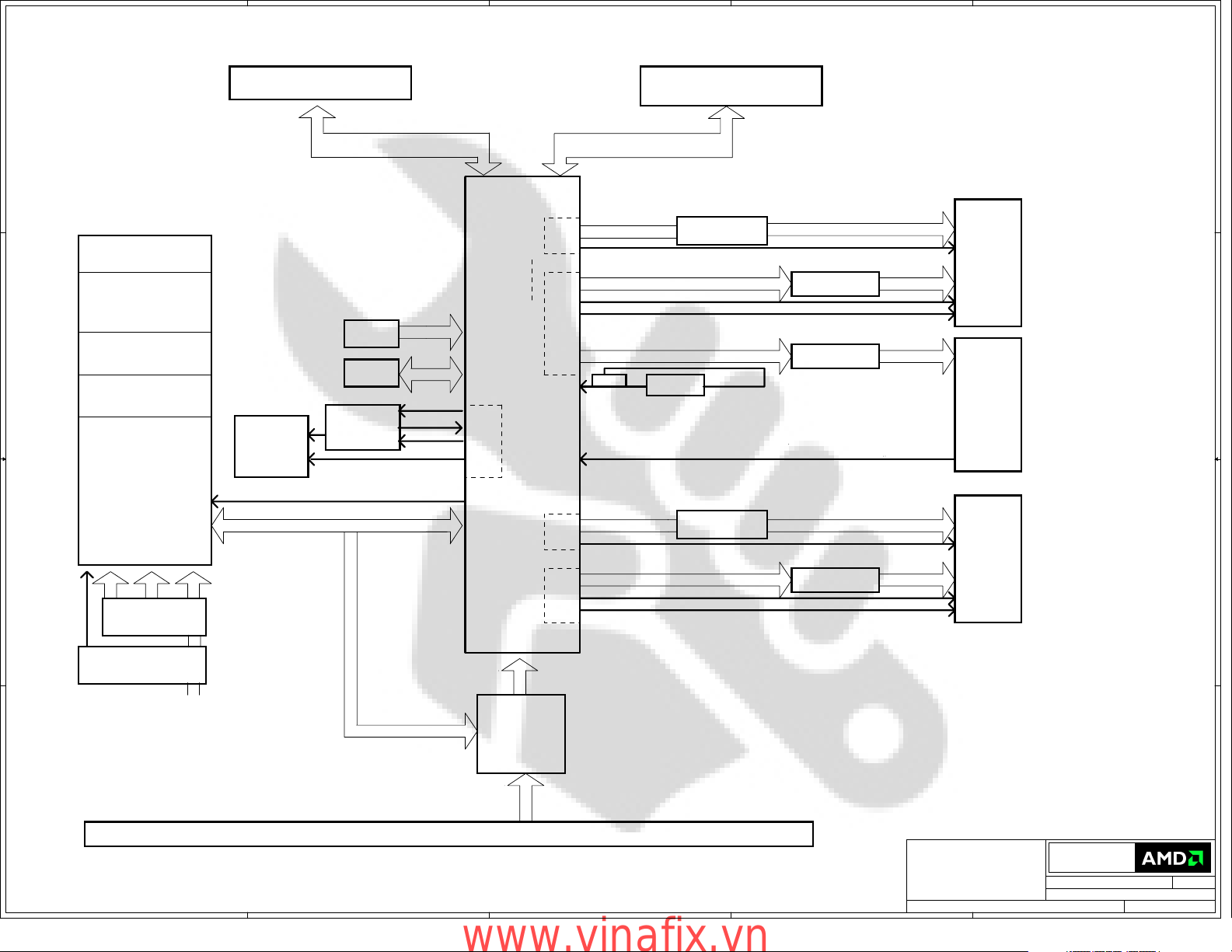
MEMORY CHANNEL A
DDR2 4pcs 16Mx32 (256MB)
D D
Channel A
Channel B
MEMORY CHANNEL B
DDR2 4pcs 16Mx32 (256MB)
TMDS1
Oscillator
Shunt Resistors
Shunt Resistors
XTALIN/OUT
RBG Filters
TVO Filters
RBG Filters
HPD1
Slim-VGA
Connector
TVO
Connector
HPD2
DVI-I
Slim-VGA
Connector
&HDMI
&
DL TMDS1
POWER REGULATORS
From +12V_EXT
+VDDC (MPVDD, VDDCI,
B_VDDC, B_PCIE)
FAN
C C
B B
From +5V_BUS:
+MPVDD
From +MVDD Linear (1.1V):
PCIE_VDDC, DPLL_VDDC
From +3.3V_BUS:
Direct or Linear (1.8V)
VDD_CT, DPLL_PVDD,
TPVDD, T2PVDD,
TXVDDR,
T2XVDDR(LTVDD18),
T2XVDDC(LTVDD33),
AVDD, A2VDD, VDD1DI,
VDD2DI,
PCIE_VDDR, PCIE_PLL,
VDDR3, VDDR4, VDDR5,
+B_VDDC_CT
+3.3V
+5V_BUS
3.3V_BUS
delayed circuit
+12V_BUS
FAN
POWER DELIVERY
Straps
BIOS
Speed control
& temperature
sense
Built-in PWM
INTERRUPT
Temp. Sensing
Dynamic VDDC
GPIO
ROM
Thermal
DDC3
GPIO17
D+/D-
TS_FDO
GPIO15
RV630
CTFb
HPD1
DAC2
CRT2
H/V2Sync
DDC2
XTALIN/OUT
GENERICA
TMDS2
DL TMDS2
HPD2
(GPIO14)
DAC1
CRT1
H/VSync
DDC1
TVO
XTAL
STV/HDTV#_OUT_DET
PCI-Express
SMPS Enable
Circuit
SEFADU HDMI: RH AGP RV630
256MB/512MB DDR2
+3.3V_BUS
+5V_BUS
+12V_BUS
RIALTO
DVI-I ,TVO,HDMI FH
REV 0
AGP 8X/4X
A A
AGP CONNECTOR
5
4
3
2
CONFIDENTIAL & PROPRIETARY TO ADVANCED MICRO DEVICES INC.
CONFIDENTIAL & PROPRIETARY TO ADVANCED MICRO DEVICES INC.
CONFIDENTIAL & PROPRIETARY TO ADVANCED MICRO DEVICES INC.
© 2007 Advanced Micro Devices
© 2007 Advanced Micro Devices
© 2007 Advanced Micro Devices
This AMD Board schematic and design is the exclusive property of AMD,
This AMD Board schematic and design is the exclusive property of AMD,
This AMD Board schematic and design is the exclusive property of AMD,
and is provided only to entities under a non-disclosure agreement
and is provided only to entities under a non-disclosure agreement
and is provided only to entities under a non-disclosure agreement
with AMD for evaluation purposes. Further distribution or disclosure
with AMD for evaluation purposes. Further distribution or disclosure
with AMD for evaluation purposes. Further distribution or disclosure
is strictly prohibited. Use of this schematic and design for any purpose
is strictly prohibited. Use of this schematic and design for any purpose
is strictly prohibited. Use of this schematic and design for any purpose
other than evaluation requires a Board Technology License Agreement
other than evaluation requires a Board Technology License Agreement
other than evaluation requires a Board Technology License Agreement
with AMD. AMD makes no representations or warranties of any kind
with AMD. AMD makes no representations or warranties of any kind
with AMD. AMD makes no representations or warranties of any kind
regarding this schematic and design, including, not limited to,
regarding this schematic and design, including, not limited to,
regarding this schematic and design, including, not limited to,
any implied warranty of merchantibility or fitness for a particular
any implied warranty of merchantibility or fitness for a particular
any implied warranty of merchantibility or fitness for a particular
purpose, and disclaims responsibility forany consequences resulting
purpose, and disclaims responsibility forany consequences resulting
purpose, and disclaims responsibility forany consequences resulting
from use of the information included herein.
from use of the information included herein.
from use of the information included herein.
Title
Title
Title
RV630 DDR2-BLOCK DIAGRAM
RV630 DDR2-BLOCK DIAGRAM
RV630 DDR2-BLOCK DIAGRAM
Advanced Micro Devices Inc.
Advanced Micro Devices Inc.
Advanced Micro Devices Inc.
1 Commerce Valley Drive East
1 Commerce Valley Drive East
1 Commerce Valley Drive East
Markham, Ontario
Markham, Ontario
Markham, Ontario
Friday, May 04, 2007
Friday, May 04, 2007
Friday, May 04, 2007
Sheet
Sheet
Sheet
of
123
of
123
of
123
1
Doc No.
Doc No.
Doc No.
RevDate:
RevDate:
RevDate:
0
0
0
105-B281xx-00A
105-B281xx-00A
105-B281xx-00A
www.vinafix.vn
Page 3
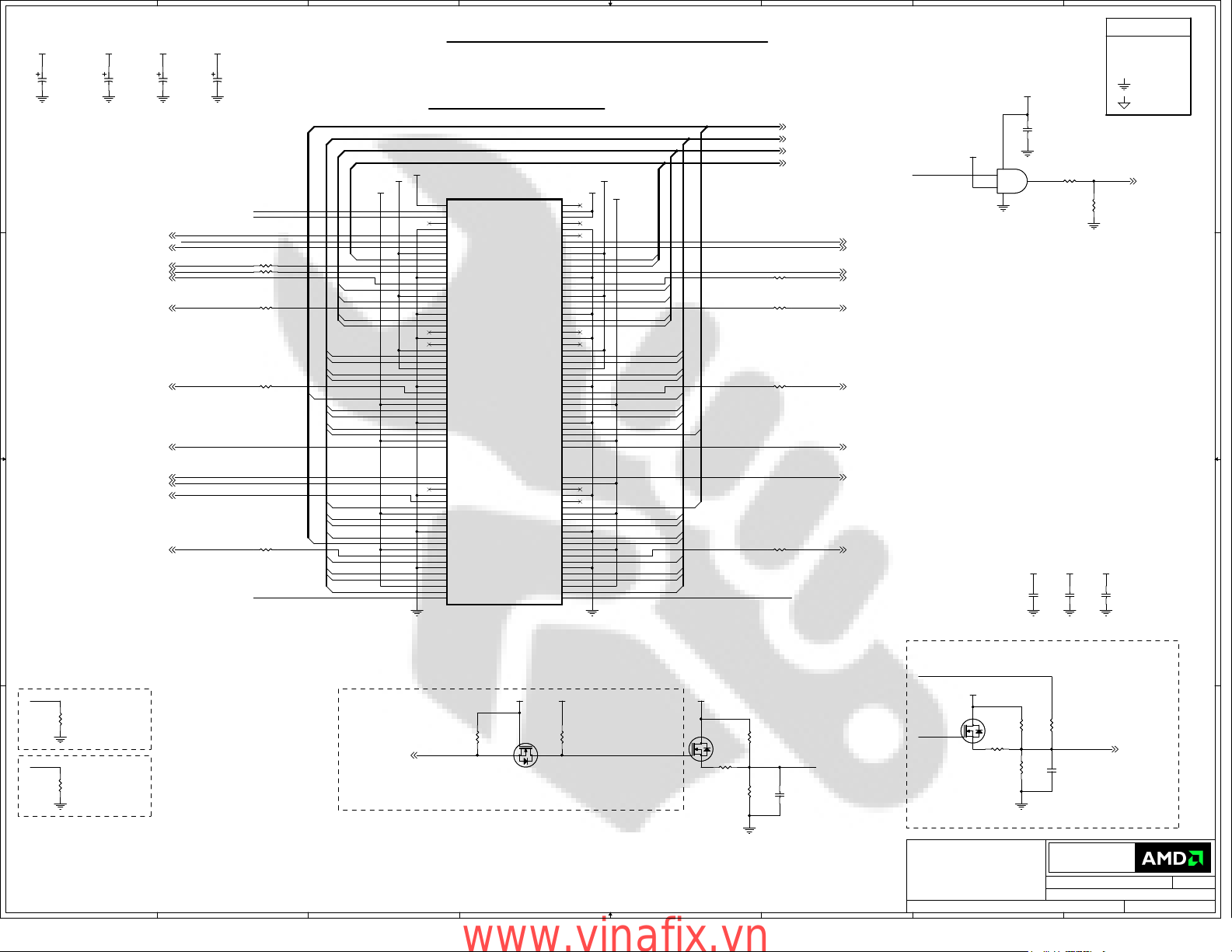
8
LAYOUT NOTE: SOME OF THE CAPS BELOW MAY BE
REMOVED IF SPACE IS AN ISSUE, ASK BEFORE REMOVING
+12V_BUS
C1509
C1509
10uF_20V
10uF_20V
D D
C C
+5V_BUS +3.3V_BUS
C1506
C1506
47uF_6.3V
47uF_6.3V
AGP_INTR#(3)
AGP_GNT#(3)
AGP_MB_8X_DET#(3)
AGP_DBI_HI(3)
AGP_WBF#(3)
AGP_SBSTB#(3)
AGP_ADSTB1#(3)
AGP_FRAME#(3)
C1501
C1501
47uF_6.3V
47uF_6.3V
+VDDQ_BUS
C1508
C1508
100uF_6.3V
100uF_6.3V
AGP_CON_RESET#
7
Use 47uF Tant. 16V 20% D size (P/N 4230047600),
800mR Max. ESR and Max. ripple 430mA @ 100kHz
or
100uF, Alum. 6.3V 20% 6.3mm dia (P/N 4261010700),
440mR Max. ESR and Max. ripple 230mA @ 100kHz
or
47uF, Alum. 6.3V 20% 5mm dia (P/N 4262047600),
760mR Max. ESR and Max. ripple 150mA @ 100kHz
Place C2 on left side of AGP connector
+VDDQ_BUS
AGP_TYPEDET#
AGP_GC_8X_DET#
AGP_ST1
R1509 0RR1509 0R
R1511 0RR1511 0R
R1504 0RR1504 0R
R1501 0RR1501 0R
AGP_MB_8X_DET#_R
AGP_DBI_HI_R
AGP_SBA1
AGP_SBA3
AGP_SBA5
AGP_SBA7
AGP_AD30
AGP_AD28
AGP_AD26
AGP_AD24
AGP_C/BE#3
AGP_AD22
AGP_AD20
AGP_AD18
AGP_AD16
6
+3.3V_BUS
AGP EDGE CONNECTOR
4X/8X AGP BUS
+12V_BUS
MAGP1
MAGP1
A1
12V
A2
TYPEDET#
A3
GC_DET#/RESERVED
A4
USB-
A5
GND
A6
INTA#
A7
RST#
A8
GNT#
A9
VCC3.3
A10
ST1
A11
MB_DET#/RESERVED
A12
DBI_HI/PIPE#
A13
GND#A13
A14
WBF#
A15
SBA1
A16
VCC3.3#A16
A17
SBA3
A18
SB_STB#
A19
GND#A19
A20
SBA5
A21
SBA7
A22
RESERVED
A23
GND#A23
A24
RESERVED#A24
A25
VCC3.3#A25
A26
AD30
A27
AD28
A28
VCC3.3#A28
A29
AD26
A30
AD24
A31
GND#A31
A32
AD_STB1#
A33
C/BE3#
A34
VDDQ1.5
A35
AD22
A36
AD20
A37
GND#A37
A38
AD18
A39
AD16
A40
VDDQ1.5#A40
A41
FRAME#
5
OVRCNT#
5.0V#B3
USB+
GND#B5
INTB#
REQ#
VCC3.3#B9
RBF#
GND#B13
DBI_LO/RESERVED
SBA0
VCC3.3#B16
SBA2
SB_STB
GND#B19
SBA4
SBA6
RESERVED#B22
GND#B23
3.3VAUX
VCC3.3#B25
AD31
AD29
VCC3.3#B28
AD27
AD25
GND#B31
AD_STB1
AD23
VDDQ1.5#B34
AD21
AD19
GND#B37
AD17
C/BE2#
VDDQ1.5#B40
IRDY#
4
AGP_C/BE#[3..0]
AGP_AD[31..0]
AGP_SBA[7..0]
AGP_ST[2..0]
+3.3V_BUS
+5V_BUS
+VDDQ_BUS
B1
B2
5.0V
B3
B4
B5
B6
B7
CLK
B8
B9
B10
ST0
B11
ST2
B12
B13
B14
B15
B16
B17
B18
B19
B20
B21
B22
B23
B24
B25
B26
B27
B28
B29
B30
B31
B32
B33
B34
B35
B36
B37
B38
B39
B40
B41
AGP_ST0
AGP_ST2
AGP_SBA0
AGP_SBA2
AGP_SBA4
AGP_SBA6
AGP_AD31
AGP_AD29
AGP_AD27
AGP_AD25
AGP_AD23
AGP_AD21
AGP_AD19
AGP_AD17
AGP_C/BE#2
AGP_DBI_LO_R
AGP_SBSTB_R
AGP_ADSTB1_R
R1500 0RR1500 0R
R1510 0RR1510 0R
R1516 0RR1516 0R
AGP_C/BE#[3..0] (3)
AGP_AD[31..0] (3)
AGP_SBA[7..0] (3)
AGP_ST[2..0] (3)
3
AGP_AGPCLK (3)
AGP_REQ# (3)
AGP_RBF# (3)
AGP_DBI_LO (3)
AGP_SBSTB (3)
AGP_ADSTB1 (3)
AGP_IRDY# (3)
AGP_CON_RESET#
+5V_BUS
2
+5V_BUS
C1500
C1500
100nF
100nF
53
U1501
U1501
1
2
R1519 100RR1519 100R
4
NC7SZ08P5X_NL
NC7SZ08P5X_NL
R1520
R1520
180R
180R
1
SYMBOL LEGEND
DO NOT
DNI
INSTALL
#
ACTIVE
LOW
DIGITAL
GROUND
ANALOG
GROUND
AGP_RESET# (3)
AGP_TRDY#(3)
AGP_STOP#(3)
AGP_PAR(3)
AGP_ADSTB0#(3)
B B
R1508 0RR1508 0R
AGP_VREFGC
AGP_PAR_R
AGP_AD15
AGP_AD13
AGP_AD11
AGP_AD9
AGP_C/BE#0
AGP_AD6
AGP_AD4
AGP_AD2
A46
A47
A48
A49
A50
A51
A52
A53
A54
A55
A56
A57
A58
A59
A60
A61
A62
A63
A64
A65
A66
TRDY#
STOP#
PME#
GND#A49
PAR
AD15
VDDQ1.5#A52
AD13
AD11
GND#A55
AD9
C/BE0#
VDDQ1.5#A58
AD_STB0#
AD6
GND#A61
AD4
AD2
VDDQ1.5#A64
AD0
VREFGC
1.5V_AGP_BUS
1.5V_AGP_BUS
DEVSEL#
VDDQ1.5#B47
PERR#
GND#B49
SERR#
C/BE1#
VDDQ1.5#B52
AD14
AD12
GND#B55
AD10
VDDQ1.5#B58
AD_STB0
GND#B61
VDDQ1.5#B64
VREFCG
B46
B47
B48
B49
B50
B51
B52
B53
B54
B55
B56
B57
AD8
B58
B59
B60
AD7
B61
B62
AD5
B63
AD3
B64
B65
AD1
B66
AGP_C/BE#1
AGP_AD14
AGP_AD12
AGP_AD10
AGP_AD8
AGP_AD7
AGP_AD5
AGP_AD3
AGP_AD1AGP_AD0
AGP_ADSTB0_R
AGP_AGPREF
R1505 0RR1505 0R
AGP_DEVSEL# (3)
AGP_ADSTB0 (3)
+12V_BUS
C1505
C1505
100nF
100nF
+5V_BUS
C1507
C1507
100nF
100nF
+3.3V_BUS
C1503
C1503
100nF
100nF
Caps for EMI - install close to AGP connector
UNIVERSAL VREFCG CIRCUIT (4X, 8X)
UNIVERSAL VREFGC CIRCUIT (4X, 8X)
AGP_TYPEDET#
AGP_GC_8X_DET#
A A
R1512
R1512
5.1R
5.1R
R15180RR1518
0R
+12V, TYPEDET#
short protection
for OEM (5.1R)
8
AGP_MB_8X_DET#(3)
7
AGP_MB_8X_DET#
6
R1517
R1517
47K
47K
+3.3V_BUS
1
Q1500
Q1500
5
32
BSN20
BSN20
+12V_BUS
R1503
R1503
20K
20K
TEST
+VDDQ_BUS
1
4
32
Q1501
Q1501
R1514
R1514
324R
324R
402
2N7002E
2N7002E
R1515
R1515
147R
147R
R1513
R1513
100R
100R
AGP_VREFGC
C1502
C1502
10nF
10nF
3
AGP_AGPREF
+VDDQ_BUS
32
TEST
1
Q1502
Q1502
2N7002E
2N7002E
R1502
R1502
147R
147R
CONFIDENTIAL & PROPRIETARY TO ADVANCED MICRO DEVICES INC.
CONFIDENTIAL & PROPRIETARY TO ADVANCED MICRO DEVICES INC.
CONFIDENTIAL & PROPRIETARY TO ADVANCED MICRO DEVICES INC.
© 2007 Advanced Micro Devices
© 2007 Advanced Micro Devices
© 2007 Advanced Micro Devices
This AMD Board schematic and design is the exclusive property of AMD,
This AMD Board schematic and design is the exclusive property of AMD,
This AMD Board schematic and design is the exclusive property of AMD,
and is provided only to entities under a non-disclosure agreement
and is provided only to entities under a non-disclosure agreement
and is provided only to entities under a non-disclosure agreement
with AMD for evaluation purposes. Further distribution or disclosure
with AMD for evaluation purposes. Further distribution or disclosure
with AMD for evaluation purposes. Further distribution or disclosure
is strictly prohibited. Use of this schematic and design for any purpose
is strictly prohibited. Use of this schematic and design for any purpose
is strictly prohibited. Use of this schematic and design for any purpose
other than evaluation requires a Board Technology License Agreement
other than evaluation requires a Board Technology License Agreement
other than evaluation requires a Board Technology License Agreement
with AMD. AMD makes no representations or warranties of any kind
with AMD. AMD makes no representations or warranties of any kind
with AMD. AMD makes no representations or warranties of any kind
regarding this schematic and design, including, not limited to,
regarding this schematic and design, including, not limited to,
regarding this schematic and design, including, not limited to,
any implied warranty of merchantibility or fitness for a particular
any implied warranty of merchantibility or fitness for a particular
any implied warranty of merchantibility or fitness for a particular
purpose, and disclaims responsibility forany consequences resulting
purpose, and disclaims responsibility forany consequences resulting
purpose, and disclaims responsibility forany consequences resulting
from use of the information included herein.
from use of the information included herein.
from use of the information included herein.
Title
Title
Title
RH AGP RV560 256MB GDDR3 DUAL DL-DVI-I VIVO
RH AGP RV560 256MB GDDR3 DUAL DL-DVI-I VIVO
RH AGP RV560 256MB GDDR3 DUAL DL-DVI-I VIVO
2
RIALTO
RIALTO
R1506
R1506
R1521
R1521
0R
324R
324R
0R
AGP_AGPREFCG
R1507
R1507
C1504
C1504
100R
100R
10nF
10nF
Advanced Micro Devices Inc.
Advanced Micro Devices Inc.
Advanced Micro Devices Inc.
1 Commerce Valley Drive East
1 Commerce Valley Drive East
1 Commerce Valley Drive East
Markham, Ontario
Markham, Ontario
Markham, Ontario
Friday, May 04, 2007
Friday, May 04, 2007
Friday, May 04, 2007
Sheet
Sheet
Sheet
223
223
223
of
of
of
AGP_AGPREFCG (3)
Doc No.
Doc No.
Doc No.
105-B281xx-00A
105-B281xx-00A
105-B281xx-00A
1
RevDate:
RevDate:
RevDate:
0
0
0
www.vinafix.vn
Page 4
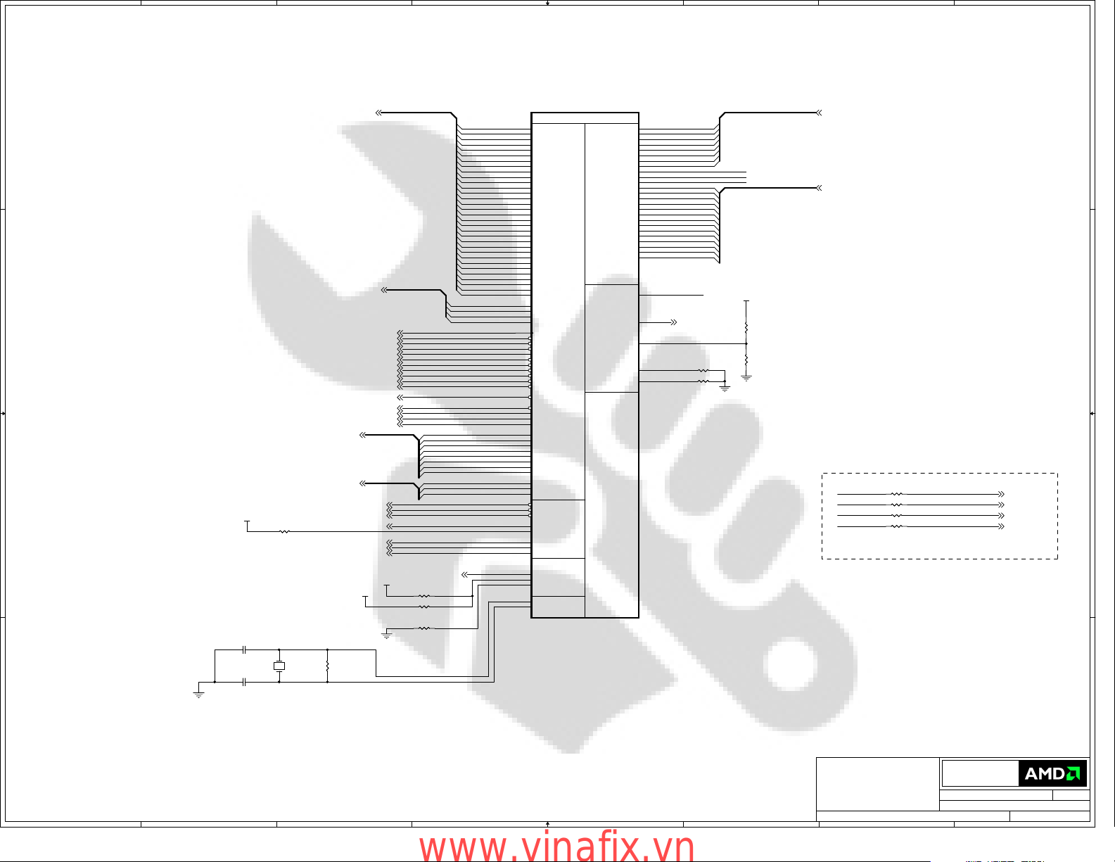
8
7
6
5
4
3
2
1
D D
C C
B B
+VDDQ_BUS
R1529 47RR1529 47R
C1511
C1511
18pF_50V
18pF_50V
C1510
C1510
18pF_50V
18pF_50V
2 1
Y1500
Y1500
25.000MHz
25.000MHz
AGP_AD[31..0](2)
AGP_C/BE#[3..0](2)
AGP_SBA[7..0](2)
AGP_ST[2..0](2)
AGP_ADSTB0#(2)
AGP_ADSTB1#(2)
AGP_AGPREFCG(2)
AGP_MB_8X_DET#(2)
R15321MR1532
1M
AGP_SBSTB#(2)
AGP_DBI_LO(2)
AGP_DBI_HI(2)
+3.3V
AGP_ADSTB0(2)
AGP_ADSTB1(2)
AGP_AGPCLK(2)
AGP_RESET#(2)
AGP_STOP#(2)
AGP_DEVSEL#(2)
AGP_TRDY#(2)
AGP_IRDY#(2)
AGP_FRAME#(2)
AGP_INTR#(2)
AGP_WBF#(2)
AGP_SBSTB(2)
AGP_REQ#(2)
AGP_GNT#(2)
AGP_RBF#(2)
+VDDQ_BUS
AGP_PAR(2)
AGP_SBA[7..0]
AGP_ST[2..0]
AGP_AD[31..0]
AGP_C/BE#[3..0]
R1526 1KR1526 1K
R1593 1KRIALTOR1593 1KRIALTO
R1528 1KR1528 1K
U1500B
U1500B
AGP_AD0
AGP_AD1
AGP_AD2
AGP_AD3
AGP_AD4
AGP_AD5
AGP_AD6
AGP_AD7
AGP_AD8
AGP_AD9
AGP_AD10
AGP_AD11
AGP_AD12
AGP_AD13
AGP_AD14
AGP_AD15
AGP_AD16
AGP_AD17
AGP_AD18
AGP_AD19
AGP_AD20
AGP_AD21
AGP_AD22
AGP_AD23
AGP_AD24
AGP_AD25
AGP_AD26
AGP_AD27
AGP_AD28
AGP_AD29
AGP_AD30
AGP_AD31
AGP_C/BE#0
AGP_C/BE#1
AGP_C/BE#2
AGP_C/BE#3
AGP_SBA0
AGP_SBA1
AGP_SBA2
AGP_SBA3
AGP_SBA4
AGP_SBA5
AGP_SBA6
AGP_SBA7
AGP_ST0
AGP_ST1
AGP_ST2
STP_AGPB(6)
A6
A5
B6
B5
C5
C4
C3
D4
E4
F4
F3
G4
G3
H3
H4
J3
F6
F5
G6
H7
H6
J6
J7
K7
L7
M7
M6
M5
N7
N6
P7
P6
E3
J4
G7
J5
AA2
AB3
U6
V5
E7
F7
L4
L3
M3
M4
W4
R7
T6
D2
K6
R3
U4
U3
T4
T3
P4
P3
N4
N3
W3
V4
V3
R4
C2
L6
D6
E6
R5
R6
T7
AA3
AA4
Y3
AA8
AB8
Rialto A11
Rialto A11
AD_0
AD_1
AD_2
AD_3
AD_4
AD_5
AD_6
AD_7
AD_8
AD_9
AD_10
AD_11
AD_12
AD_13
AD_14
AD_15
AD_16
AD_17
AD_18
AD_19
AD_20
AD_21
AD_22
AD_23
AD_24
AD_25
AD_26
AD_27
AD_28
AD_29
AD_30
AD_31
C_BEB_0
C_BEB_1
C_BEB_2
C_BEB_3
PCICLK
RSTB
REQB
GNTB
PAR
STOPB
DEVSELB
TRDYB
IRDYB
FRAMEB
INTAB
WBFB
RBFB
AD_STBF_0
AD_STBF_1
SB_STBF
SBA_0
SBA_1
SBA_2
SBA_3
SBA_4
SBA_5
SBA_6
SBA_7
ST_0
ST_1
ST_2
SB_STBS
AD_STBS_0
AD_STBS_1
AGPVREF
AGPTEST
DBI_LO
DBI_HI
AGP8X_DETB
STP_AGPB
AGP_BUSYB
RSTB_MSK
XTO
XTI
PART 2 OF 4
PART 2 OF 4
PCI / AGPAGP2X
PCI / AGPAGP2X
4X8X
4X8X
AGP
AGP
AGP
Additional
AGP
Additional
CLK
CLK
GPIOMISC
GPIOMISC
NC
NC
GPIO_0
GPIO_1
GPIO_2
GPIO_3
GPIO_4
GPIO_5
GPIO_6
GPIO_7
GPIO_8
GPIO_9
GPIO_10
GPIO_11
GPIO_12
GPIO_13
GPIO_14
GPIO_15
GPIO_16
GPIO_17
GPIO_18
GPIO_19
GPIO_20
GPIO_21
GPIO_22
GPIO_23
GPIO_24
ROMCSB
REFCLKBYP
VrefG1
PLLTEST
TESTEN
Y9
AB10
AA10
Y10
AA11
Y12
AA12
AB12
W18
Y20
AB20
AA13
AB13
AA14
AB14
AA15
AB15
AA16
AB16
AA17
AB17
AA18
AB18
Y18
AA19
Y19
W20
AB4
W6
Y4
B_GPIO0
B_GPIO1
B_GPIO2
B_GPIO3
B_GPIO4
B_GPIO5
B_GPIO6
B_GPIO7
B_GPIO11
B_GPIO12
B_GPIO13
B_GPIO14
B_GPIO15
B_GPIO16
B_GPIO17
B_GPIO18
B_GPIO19
B_GPIO20
B_GPIO21
B_GPIO22
B_GPIO23
B_GPIO24
B_ROMCS#
REFCLKBYP (6)
R1527 1KR1527 1K
R1533 1KR1533 1K
B_GPIO8
B_GPIO9
B_GPIO10
+3.3V
R1531
R1531
499R
499R
R1530
R1530
499R
499R
B_GPIO[7..0]
B_GPIO[24..11]
B_GPIO[7..0] (6)
B_GPIO[24..11] (6)
B_GPIO8
B_GPIO9
B_GPIO10
B_ROMCS#
R1523 33RR1523 33R
R1522 33RR1522 33R
R1524 33RR1524 33R
R1525 33RR1525 33R
TO SERIAL EEPROM 512K/1M
ROM_SO (12)
SI/A16 (12)
SCK/WEb (12)
CSb (12)
A A
CONFIDENTIAL & PROPRIETARY TO ADVANCED MICRO DEVICES INC.
CONFIDENTIAL & PROPRIETARY TO ADVANCED MICRO DEVICES INC.
CONFIDENTIAL & PROPRIETARY TO ADVANCED MICRO DEVICES INC.
© 2007 Advanced Micro Devices
© 2007 Advanced Micro Devices
© 2007 Advanced Micro Devices
This AMD Board schematic and design is the exclusive property of AMD,
This AMD Board schematic and design is the exclusive property of AMD,
This AMD Board schematic and design is the exclusive property of AMD,
and is provided only to entities under a non-disclosure agreement
and is provided only to entities under a non-disclosure agreement
and is provided only to entities under a non-disclosure agreement
with AMD for evaluation purposes. Further distribution or disclosure
with AMD for evaluation purposes. Further distribution or disclosure
with AMD for evaluation purposes. Further distribution or disclosure
is strictly prohibited. Use of this schematic and design for any purpose
is strictly prohibited. Use of this schematic and design for any purpose
is strictly prohibited. Use of this schematic and design for any purpose
other than evaluation requires a Board Technology License Agreement
other than evaluation requires a Board Technology License Agreement
other than evaluation requires a Board Technology License Agreement
with AMD. AMD makes no representations or warranties of any kind
with AMD. AMD makes no representations or warranties of any kind
with AMD. AMD makes no representations or warranties of any kind
regarding this schematic and design, including, not limited to,
regarding this schematic and design, including, not limited to,
regarding this schematic and design, including, not limited to,
any implied warranty of merchantibility or fitness for a particular
any implied warranty of merchantibility or fitness for a particular
any implied warranty of merchantibility or fitness for a particular
purpose, and disclaims responsibility forany consequences resulting
purpose, and disclaims responsibility forany consequences resulting
purpose, and disclaims responsibility forany consequences resulting
from use of the information included herein.
from use of the information included herein.
from use of the information included herein.
Title
Title
Title
RH AGP RV560 256MB GDDR3 DUAL DL-DVI-I VIVO
RH AGP RV560 256MB GDDR3 DUAL DL-DVI-I VIVO
8
7
6
5
4
3
RH AGP RV560 256MB GDDR3 DUAL DL-DVI-I VIVO
2
Advanced Micro Devices Inc.
Advanced Micro Devices Inc.
Advanced Micro Devices Inc.
1 Commerce Valley Drive East
1 Commerce Valley Drive East
1 Commerce Valley Drive East
Markham, Ontario
Markham, Ontario
Markham, Ontario
Friday, May 04, 2007
Friday, May 04, 2007
Friday, May 04, 2007
Sheet
Sheet
Sheet
of
323
of
323
of
323
Doc No.
Doc No.
Doc No.
1
RevDate:
RevDate:
RevDate:
0
0
0
105-B281xx-00A
105-B281xx-00A
105-B281xx-00A
www.vinafix.vn
Page 5
8
D D
7
6
5
4
3
2
1
Rialto ASIC p/n is: 218BAPAGA11F
U1500A
U1500A
W16
W11
W19
R1541
R1541
4.7K
4.7K
U13
T13
T14
R14
R12
P12
P13
N13
N14
M14
M12
L12
L13
K13
K14
J14
J12
H12
H13
G13
G14
F14
F12
E12
E13
D13
D14
C14
C12
B12
B13
A13
V16
Y11
R20
PCIE_TX0P
PCIE_TX0N
PCIE_TX1P
PCIE_TX1N
PCIE_TX2P
PCIE_TX2N
PCIE_TX3P
PCIE_TX3N
PCIE_TX4P
PCIE_TX4N
PCIE_TX5P
PCIE_TX5N
PCIE_TX6P
PCIE_TX6N
PCIE_TX7P
PCIE_TX7N
PCIE_TX8P
PCIE_TX8N
PCIE_TX9P
PCIE_TX9N
PCIE_TX10P
PCIE_TX10N
PCIE_TX11P
PCIE_TX11N
PCIE_TX12P
PCIE_TX12N
PCIE_TX13P
PCIE_TX13N
PCIE_TX14P
PCIE_TX14N
PCIE_TX15P
PCIE_TX15N
PCIE_REFCLKP
PCIE_REFCLKN
RefCLKP
RefCLKN
PERSTB
PCIETEST
Rialto A11
Rialto A11
PETp0_GFXRp0(7)
PETn0_GFXRn0(7)
PETp1_GFXRp1(7)
PETn1_GFXRn1(7)
PETp2_GFXRp2(7)
PETn2_GFXRn2(7)
PETp3_GFXRp3(7)
PETn3_GFXRn3(7)
PETp4_GFXRp4(7)
R1538 49.9RR1538 49.9R
1%
R1540 49.9RR1540 49.9R
1%
PETn4_GFXRn4(7)
PETp5_GFXRp5(7)
PETn5_GFXRn5(7)
PETp6_GFXRp6(7)
PETn6_GFXRn6(7)
PETp7_GFXRp7(7)
PETn7_GFXRn7(7)
PETp8_GFXRp8(7)
PETn8_GFXRn8(7)
PETp9_GFXRp9(7)
PETn9_GFXRn9(7)
PETp10_GFXRp10(7)
PETn10_GFXRn10(7)
PETp11_GFXRp11(7)
PETn11_GFXRn11(7)
PETp12_GFXRp12(7)
PETn12_GFXRn12(7)
PETp13_GFXRp13(7)
PETn13_GFXRn13(7)
PETp14_GFXRp14(7)
PETn14_GFXRn14(7)
PETp15_GFXRp15(7)
PETn15_GFXRn15(7)
R1539 33.2RR1539 33.2R
1%
R1534 33.2RR1534 33.2R
1%
Place the reisitors
close to ASIC
C C
B B
PCIE_REFCLKP(7)
PCIE_REFCLKN(7)
PERST#(7)
PART 1 OF 4
PART 1 OF 4
PCIE TX
PCIE TX
Clock
Clock
V17
PCIE_RX0P
U17
PCIE_RX0N
PCIE_RX1P
PCIE_RX1N
PCIE_RX2P
PCIE_RX2N
PCIE_RX3P
PCIE_RX3N
PCIE_RX4P
PCIE_RX4N
PCIE_RX5P
PCIE_RX5N
PCIE_RX6P
PCIE_RX6N
PCIE_RX7P
PCIE_RX7N
PCIE_RX8P
PCIE_RX8N
PCIE RX
PCIE RX
PCIE_RX9P
PCIE_RX9N
PCIE_RX10P
PCIE_RX10N
PCIE_RX11P
PCIE_RX11N
PCIE_RX12P
PCIE_RX12N
PCIE_RX13P
PCIE_RX13N
PCIE_RX14P
PCIE_RX14N
PCIE_RX15P
PCIE_RX15N
Calibration
Calibration
PCIE_CALRN
PCIE_CALRP
PCIE_CALI
R_EXT
U19
T19
T16
R16
R17
P17
P19
N19
N16
M16
M17
L17
L19
K19
K16
J16
J17
H17
H19
G19
G16
F16
F17
E17
E19
D19
D16
C16
C17
B17
AA21
Y21
W21
Y8
1%
R1536 100RR1536 100R
R1535 150RR1535 150R
1%
R1537 10KR1537 10K
1%
R1542 750RR1542 750R
1%
P
P
C
C
I
I
-
E
E
X
X
P
P
R
R
E
E
S
S
S
S
I
I
N
N
T
T
E
E
R
R
F
F
A
A
C
C
E
E
GFXTp0_PERp0 (7)
GFXTn0_PERn0 (7)
GFXTp1_PERp1 (7)
GFXTn1_PERn1 (7)
GFXTp2_PERp2 (7)
GFXTn2_PERn2 (7)
GFXTp3_PERp3 (7)
GFXTn3_PERn3 (7)
GFXTp4_PERp4 (7)
GFXTn4_PERn4 (7)
GFXTp5_PERp5 (7)
GFXTn5_PERn5 (7)
GFXTp6_PERp6 (7)
GFXTn6_PERn6 (7)
GFXTp7_PERp7 (7)
GFXTn7_PERn7 (7)
GFXTp8_PERp8 (7)
GFXTn8_PERn8 (7)
GFXTp9_PERp9 (7)
GFXTn9_PERn9 (7)
GFXTp10_PERp10 (7)
GFXTn10_PERn10 (7)
GFXTp11_PERp11 (7)
GFXTn11_PERn11 (7)
GFXTp12_PERp12 (7)
GFXTn12_PERn12 (7)
GFXTp13_PERp13 (7)
GFXTn13_PERn13 (7)
GFXTp14_PERp14 (7)
GFXTn14_PERn14 (7)
GFXTp15_PERp15 (7)
GFXTn15_PERn15 (7)
+B_PCIE
A A
CONFIDENTIAL & PROPRIETARY TO ADVANCED MICRO DEVICES INC.
CONFIDENTIAL & PROPRIETARY TO ADVANCED MICRO DEVICES INC.
CONFIDENTIAL & PROPRIETARY TO ADVANCED MICRO DEVICES INC.
© 2007 Advanced Micro Devices
© 2007 Advanced Micro Devices
© 2007 Advanced Micro Devices
This AMD Board schematic and design is the exclusive property of AMD,
This AMD Board schematic and design is the exclusive property of AMD,
This AMD Board schematic and design is the exclusive property of AMD,
and is provided only to entities under a non-disclosure agreement
and is provided only to entities under a non-disclosure agreement
and is provided only to entities under a non-disclosure agreement
with AMD for evaluation purposes. Further distribution or disclosure
with AMD for evaluation purposes. Further distribution or disclosure
with AMD for evaluation purposes. Further distribution or disclosure
is strictly prohibited. Use of this schematic and design for any purpose
is strictly prohibited. Use of this schematic and design for any purpose
is strictly prohibited. Use of this schematic and design for any purpose
other than evaluation requires a Board Technology License Agreement
other than evaluation requires a Board Technology License Agreement
other than evaluation requires a Board Technology License Agreement
with AMD. AMD makes no representations or warranties of any kind
with AMD. AMD makes no representations or warranties of any kind
with AMD. AMD makes no representations or warranties of any kind
regarding this schematic and design, including, not limited to,
regarding this schematic and design, including, not limited to,
regarding this schematic and design, including, not limited to,
any implied warranty of merchantibility or fitness for a particular
any implied warranty of merchantibility or fitness for a particular
any implied warranty of merchantibility or fitness for a particular
purpose, and disclaims responsibility forany consequences resulting
purpose, and disclaims responsibility forany consequences resulting
purpose, and disclaims responsibility forany consequences resulting
from use of the information included herein.
from use of the information included herein.
from use of the information included herein.
Title
Title
Title
RH AGP RV560 256MB GDDR3 DUAL DL-DVI-I VIVO
RH AGP RV560 256MB GDDR3 DUAL DL-DVI-I VIVO
8
7
6
5
4
3
RH AGP RV560 256MB GDDR3 DUAL DL-DVI-I VIVO
2
Advanced Micro Devices Inc.
Advanced Micro Devices Inc.
Advanced Micro Devices Inc.
1 Commerce Valley Drive East
1 Commerce Valley Drive East
1 Commerce Valley Drive East
Markham, Ontario
Markham, Ontario
Markham, Ontario
Friday, May 04, 2007
Friday, May 04, 2007
Friday, May 04, 2007
Sheet
Sheet
Sheet
of
423
of
423
of
423
Doc No.
Doc No.
Doc No.
1
RevDate:
RevDate:
RevDate:
0
0
0
105-B281xx-00A
105-B281xx-00A
105-B281xx-00A
www.vinafix.vn
Page 6
8
D D
CONNECT +VDDC TO +B_VDDC
+VDDC
C1545
C1545
C1535
C1536
C1536
10nF
10nF
C1539
C1539
1uF_6.3V
1uF_6.3V
+3.3V
+B_PVDD
GND_B_PVSS
C1523
C1523
1uF_6.3V
1uF_6.3V
C1535
10nF
10nF
C1544
C1544
1uF_6.3V
1uF_6.3V
C1515
C1515
1uF
1uF
C1524
C1524
1uF_6.3V
1uF_6.3V
10nF
10nF
C1541
C1541
10uF_X6S
10uF_X6S
C1558
C1558
100nF
100nF
C1526
C1526
10nF
10nF
C1537
C1537
10nF
10nF
C1540
C1540
1uF_6.3V
1uF_6.3V
C C
B B
NS1 NS_VIANS1 NS_VIA
1 2
C1542
C1542
10nF
10nF
C1549
C1549
10uF_X6S
10uF_X6S
C1557
C1557
10uF_X6S
10uF_X6S
7
U1500C
U1500C
C11
VDDC_1
F9
VDDC_2
K11
VDDC_3
B11
VDDC_4
K9
VDDC_5
F11
VDDC_6
G10
VDDC_7
G11
VDDC_8
P11
VDDC_9
P10
VDDC_10
L9
VDDC_11
L11
VDDC_12
B9
VDDC_13
F10
VDDC_14
G9
VDDC_15
L10
VDDC_16
P9
VDDC_17
C9
VDDC_18
B10
VDDC_19
C10
VDDC_20
K10
VDDC_21
AB9
VDDCI
U9
VDDR3_1
W8
VDDR3_2
U10
VDDR3_3
V9
VDDR3_4
W9
VDDR3_5
AB5
PVDD
AA5
PVSS
Rialto A11
Rialto A11
PLL
PLL
NC
NC
Core
Core
GPIO
GPIO
AGP
AGP
PART 3 OF 4
PART 3 OF 4
P
P
O
O
W
W
E
E
R
R
6
PCIE_PVDD_12_1
PCIE_PVDD_12_2
PCIE_PVDD_12_3
PCIE_PVDD_12_4
PCIE_VDDR_18_2
PCIE_VDDR_18_3
PCIE_VDDR_18_4
PCIE_VDDR_18_1
PCIE_VDDR_12_1
PCIE_VDDR_12_2
PCIE_VDDR_12_3
PCIE_VDDR_12_4
PCIE_VDDR_12_5
PCI-Express
PCI-Express
PCIE_VDDR_12_6
PCIE_VDDR_12_7
PCIE_VDDR_12_8
PCIE_VDDR_12_9
AGPDIFF
AGPDIFF
Volt COV
Volt COV
OSC
OSC
I/O
I/O
PCIE_PVDD_18
VDDP_1
VDDP_2
VDDP_3
VDDP_4
VDDP_5
VDDP_6
VDDP_7
VDDP_8
VDDP_9
VDDP_10
VDDP_11
VDDP_12
VDDP_13
VDDP_14
VDDP_15
VDDP_16
VDDP_17
VDDP_18
VDDP_19
VDDP_20
VDDP_21
VDDP_22
VDDP_23
VDDP_24
VDD15_1
VDD15_2
VDD15_3
VDD15_4
VDD15_5
VAA_DIO
AGND_DIO_1
AGND_DIO_2
VAA_XTL
AGND_XTL_1
AGND_XTL_2
5
+B_PCIE
+B_PCIE_PVDD_18
C1514
C1514
1uF_6.3V
C1552
C1552
10nF
10nF
C1554
C1554
10nF
10nF
C1520
C1520
10nF
10nF
C1530
C1530
100nF
100nF
C1532
C1532
100nF
100nF
1uF_6.3V
C1553
C1553
10nF
10nF
C1521
C1521
10nF
10nF
+VDDQ_BUS
+B_VDDC_CT
C1556
C1556
10nF
10nF
C1529
C1529
10uF_X6S
10uF_X6S
C1531
C1531
10uF_X6S
10uF_X6S
+B_PCIE
C1560
C1560
1uF_6.3V
1uF_6.3V
GND_XTL
C1512
C1512
10nF
10nF
C1522
C1522
1uF_6.3V
1uF_6.3V
C1555
C1555
1uF_6.3V
1uF_6.3V
+VAA_XTL
C1516
C1516
1uF
1uF
GND_DIO
C1518
C1518
1uF
1uF
C1513
C1513
1uF_6.3V
1uF_6.3V
+VAA_DIO
NS2NS_VIA NS2NS_VIA
NS3NS_VIA NS3NS_VIA
12
F21
A21
B21
E21
A15
A16
A17
A18
A19
W13
Y13
Y14
W12
W14
Y16
W15
Y15
Y17
A4
E2
G2
L2
U2
W2
AB2
G5
K4
B4
T5
W5
B2
N2
E5
D8
E8
C8
H8
J8
M8
N8
R8
A2
B8
U8
A8
T9
V8
AB6
AA6
Y6
AB7
AA7
Y7
4
12
T17
L21
W17
C21
B19
C19
D18
E18
G18
H18
K18
L18
M19
N18
P18
M18
R19
T18
L16
H16
E16
B16
T15
P16
F15
L15
G17
K17
F18
U18
U12
V15
B18
B15
C15
D15
E15
G15
H15
J15
K15
M15
N15
P15
R15
U15
V18
V14
R18
A14
C13
P14
L14
F13
B14
J13
E14
M13
V12
U16
H14
U14
V13
J21
R13
A20
G21
A12
K21
B20
C20
D20
E20
F20
G20
H20
L20
T20
F19
J19
C18
J18
D17
N17
D12
G12
N12
T12
K12
V10
V11
W7
T11
U11
W10
3
U1500D
U1500D
PCIE_VSS_1
PCIE_VSS_2
PCIE_VSS_3
PCIE_VSS_4
PCIE_VSS_5
PCIE_VSS_6
PCIE_VSS_7
PCIE_VSS_8
PCIE_VSS_9
PCIE_VSS_10
PCIE_VSS_11
PCIE_VSS_12
PCIE_VSS_13
PCIE_VSS_14
PCIE_VSS_15
PCIE_VSS_16
PCIE_VSS_17
PCIE_VSS_18
PCIE_VSS_19
PCIE_VSS_20
PCIE_VSS_21
PCIE_VSS_22
PCIE_VSS_23
PCIE_VSS_24
PCIE_VSS_25
PCIE_VSS_26
PCIE_VSS_27
PCIE_VSS_28
PCIE_VSS_29
PCIE_VSS_30
PCIE_VSS_31
PCIE_VSS_32
PCIE_VSS_33
PCIE_VSS_34
PCIE_VSS_35
PCIE_VSS_36
PCIE_VSS_37
PCIE_VSS_38
PCIE_VSS_39
PCIE_VSS_40
PCIE_VSS_41
PCIE_VSS_42
PCIE_VSS_43
PCIE_VSS_44
PCIE_VSS_45
PCIE_VSS_46
PCIE_VSS_47
PCIE_VSS_48
PCIE_VSS_49
PCIE_VSS_50
PCIE_VSS_51
PCIE_VSS_52
PCIE_VSS_53
PCIE_VSS_54
PCIE_VSS_55
PCIE_VSS_56
PCIE_VSS_57
PCIE_VSS_58
PCIE_VSS_59
PCIE_VSS_60
PCIE_VSS_61
PCIE_VSS_62
PCIE_VSS_63
PCIE_VSS_64
PCIE_VSS_65
PCIE_VSS_66
PCIE_VSS_67
PCIE_VSS_68
PCIE_VSS_69
PCIE_VSS_70
PCIE_VSS_71
PCIE_VSS_72
PCIE_VSS_73
PCIE_VSS_74
PCIE_VSS_75
PCIE_VSS_76
PCIE_VSS_77
PCIE_VSS_78
PCIE_VSS_79
PCIE_VSS_80
PCIE_VSS_81
PCIE_VSS_82
PCIE_VSS_83
PCIE_VSS_84
PCIE_VSS_85
PCIE_VSS_86
PCIE_VSS_87
PCIE_VSS_88
PCIE_VSS_89
VSS_29
VSS_30
VSS_31
VSS_32
VSS_33
VSS_34
Part 4 of 4
Part 4 of 4
PCI-Express GND
PCI-Express GND
GPIO GND
GPIO GND
CORE GND
CORE GND
AGP GND
AGP GND
2
VSS_10
VSS_11
VSS_12
VSS_13
VSS_14
VSS_15
VSS_16
VSS_17
VSS_18
VSS_19
VSS_20
VSS_21
VSS_22
VSS_23
VSS_24
VSS_25
VSS_26
VSS_27
VSS_28
VSSP_1
VSSP_2
VSSP_3
VSSP_4
VSSP_5
VSSP_6
VSSP_7
VSSP_8
VSSP_9
VSSP_10
VSSP_11
VSSP_12
VSSP_13
VSSP_14
VSSP_15
VSSP_16
VSSP_17
VSSP_18
VSSP_19
VSSP_20
VSSP_21
VSSP_22
VSSP_23
VSSP_24
VSSP_25
VSSP_26
VSSP_27
VSSP_28
VSSP_29
VSS_1
VSS_2
VSS_3
VSS_4
VSS_5
VSS_6
VSS_7
VSS_8
VSS_9
1
M9
A10
H11
N11
T8
E10
R9
A9
E11
N10
D10
J11
D11
J9
H9
H10
M10
M11
R10
A11
N9
D9
E9
T10
J10
R11
V7
AA9
L5
D3
H2
K2
P2
T2
C6
B3
D5
H5
K3
K5
N5
U5
Y2
P5
A7
B7
D7
U7
C7
F8
G8
K8
L8
P8
A3
V6
Y5
Rialto A11
Rialto A11
A A
CONFIDENTIAL & PROPRIETARY TO ADVANCED MICRO DEVICES INC.
CONFIDENTIAL & PROPRIETARY TO ADVANCED MICRO DEVICES INC.
CONFIDENTIAL & PROPRIETARY TO ADVANCED MICRO DEVICES INC.
© 2007 Advanced Micro Devices
© 2007 Advanced Micro Devices
© 2007 Advanced Micro Devices
This AMD Board schematic and design is the exclusive property of AMD,
This AMD Board schematic and design is the exclusive property of AMD,
This AMD Board schematic and design is the exclusive property of AMD,
and is provided only to entities under a non-disclosure agreement
and is provided only to entities under a non-disclosure agreement
and is provided only to entities under a non-disclosure agreement
with AMD for evaluation purposes. Further distribution or disclosure
with AMD for evaluation purposes. Further distribution or disclosure
with AMD for evaluation purposes. Further distribution or disclosure
is strictly prohibited. Use of this schematic and design for any purpose
is strictly prohibited. Use of this schematic and design for any purpose
is strictly prohibited. Use of this schematic and design for any purpose
other than evaluation requires a Board Technology License Agreement
other than evaluation requires a Board Technology License Agreement
other than evaluation requires a Board Technology License Agreement
with AMD. AMD makes no representations or warranties of any kind
with AMD. AMD makes no representations or warranties of any kind
with AMD. AMD makes no representations or warranties of any kind
regarding this schematic and design, including, not limited to,
regarding this schematic and design, including, not limited to,
regarding this schematic and design, including, not limited to,
any implied warranty of merchantibility or fitness for a particular
any implied warranty of merchantibility or fitness for a particular
any implied warranty of merchantibility or fitness for a particular
purpose, and disclaims responsibility forany consequences resulting
purpose, and disclaims responsibility forany consequences resulting
purpose, and disclaims responsibility forany consequences resulting
from use of the information included herein.
from use of the information included herein.
from use of the information included herein.
Title
Title
Title
RH AGP RV560 256MB GDDR3 DUAL DL-DVI-I VIVO
RH AGP RV560 256MB GDDR3 DUAL DL-DVI-I VIVO
8
7
6
5
4
3
RH AGP RV560 256MB GDDR3 DUAL DL-DVI-I VIVO
2
Advanced Micro Devices Inc.
Advanced Micro Devices Inc.
Advanced Micro Devices Inc.
1 Commerce Valley Drive East
1 Commerce Valley Drive East
1 Commerce Valley Drive East
Markham, Ontario
Markham, Ontario
Markham, Ontario
Friday, May 04, 2007
Friday, May 04, 2007
Friday, May 04, 2007
Sheet
Sheet
Sheet
of
523
of
523
of
523
Doc No.
Doc No.
Doc No.
1
RevDate:
RevDate:
RevDate:
0
0
0
105-B281xx-00A
105-B281xx-00A
105-B281xx-00A
www.vinafix.vn
Page 7
5
4
3
2
1
B_GPIO[7..0](3)
D D
Overlap pads to save space
B_GPIO[7..0]
and to prevent assembly of
both resistors.
Layout
High logic voltageGround
Signal
C C
B B
A A
B_GPIO[24..11](3)
REFCLKBYP(3)
B_GPIO[24..11]
STP_AGPB(3)
OPTION STRAPS
B_GPIO0
B_GPIO1
B_GPIO2
B_GPIO3
B_GPIO4
B_GPIO5
B_GPIO6
B_GPIO7
B_GPIO11
B_GPIO12
B_GPIO13
B_GPIO14
B_GPIO15
B_GPIO16
B_GPIO17
B_GPIO18
B_GPIO19
B_GPIO20
B_GPIO21
B_GPIO22
B_GPIO23
B_GPIO24
REFCLKBYP
STP_AGPB
R1543 10KR1543 10K
R1544 10KDNIR1544 10KDNI
R1545 10KR1545 10K
R1546 10KDNIR1546 10KDNI
R1547 10KR1547 10K
R1548 10KDNIR1548 10KDNI
R1549 10KDNIR1549 10KDNI
R1550 10KR1550 10K
R1551 10KDNIR1551 10KDNI
R1552 10KR1552 10K
R1553 10KDNIR1553 10KDNI
R1554 10KR1554 10K
R1555 10KDNIR1555 10KDNI
R1556 10KR1556 10K
R1557 10KDNIR1557 10KDNI
R1558 10KR1558 10K
R1559 10KDNIR1559 10KDNI
R1560 10KR1560 10K
R1561 10KR1561 10K
R1562 10KDNIR1562 10KDNI
R1563 10KDNIR1563 10KDNI
R1564 10KR1564 10K
R1565 10KDNIR1565 10KDNI
R1566 10KR1566 10K
R1567 10KDNIR1567 10KDNI
R1568 10KR1568 10K
R1569 10KDNIR1569 10KDNI
R1570 10KR1570 10K
R1571 10KDNIR1571 10KDNI
R1572 10KR1572 10K
R1573 10KDNIR1573 10KDNI
R1574 10KR1574 10K
R1575 10K
R1575 10K
R1576 10KR1576 10K
DNI
DNI
R1577 10KDNIR1577 10KDNI
R1578 10KR1578 10K
R1579 10KDNIR1579 10KDNI
R1580 10KR1580 10K
R1581 10KDNIR1581 10KDNI
R1582 10KR1582 10K
R1583 10KDNIR1583 10KDNI
R1584 10KR1584 10K
R1585 10KDNIR1585 10KDNI
R1586 10KR1586 10K
R1587 10KDNIR1587 10KDNI
R1588 10KR1588 10K
R1589 10KR1589 10K
R1590 10KDNIR1590 10KDNI
+3.3V
R15910RR1591
0R
PCIE_AGP_Bridge Shared Straps
STRAPS
GPIO(0)PCIE_PTX_PWRS_ENB
PCIE_PTX_DEEMPH_EN PCI Express transmitter de-emphasis enable
PCIE_ICP (1:0)
PCIE_PTX_IEXT GPIO(4)0PCI Express transmitter extra ouptput current
DEBUG_ACCESS 1 - Set the debug bus muxes to bring out debug signals even if registers are inaccessable
PCIE_PPLL_BW GPIO(6) PCI Express PLL bandwidth setting
PCIE_REVERSE_ALL GPIO(7)00 - Don't reverse physical PCIE lanes
PCI_RETRY_ENb
MULTIFUNC
PCIE_FORCE_
COMPLIANCE
PCIE_LINK_TIMEOUT
_OVERRIDE
MOBILE_EN REFCLKBYP
BUS_PCI_CFG_
RETRY_Enb
GPIO(1)
GPIO(3:2)
GPIO(5)
GPIO(13)
GPIO(24, 14)VGA_MONO_MODE(1:0)
GPIO(15)REFCLK_LINK_CONFIG One of the strap bit to encode the combination of:
GPIO(16)
GPIO(18:17)AGPFBSKEW(1:0)
GPIO(20:19)X1CLK_SKEW(1:0)
GPIO(21)BUSCFG Control BUS type, CLK PLL select
GPIO(22)AGP_ONLY
GPIO(23)
STP_AGPB
DESCRIPTIONPIN
PCI Express transmitter power-saving enable bar
0 - 50% Tx output swing for mobile applications
1 - Full output swing
0 - de-emphasis disenable
1 - de-emphasis enable
Charge pump current setting
00 - 5.0uA
01 - 10.0uA
10 - 15.0uA
11 - 20.0uA
0 - no extra current
1 - extra current in output stage
0 - Full PLL bandwidth
1 - Reduces PLL bandwidth
1 - Reverse physical PCIE lanes
If no ROM attached, comtrols chip IDis. If rom attached identifies ROM type
00 - No ROM, CHG_ID=0
01 - 512Kb Serial AT25F512 ROM (Atmel) or AT24F1024 ROM (Atmel)
10 - 512K Serial M25P05A ROM (ST) or PM25LV512 (PMC)
11 - 1M Serial M25P10A ROM (ST) or PM25LV010 (PMC)
0 - Enable all PCI read/write retry, retry cycle 0x3
1 - Disable PCI read/write retry
00 - only VGA controller
01 - only MONO controller
10 - neither VGA/MONO controller
11 - both VGA/MONO controller
SEND_LINK_TRAINING_IMMEDIATELY
MOBILE_EN
AGP_ONLY
....
etc,
For MULTIFUNC, when TESTEN(pin)=0,
0 = 00 - Single function device
1 = 01 - Two function device. No AGP in either function
For PCIE_FORCE_COMPLIANCE, when TESTEN(pin)=1,
0 - Normal operation
1 - Force LC into compliance mode
AGP 1xclock feedback phase adjustment wrt refclk(cpuclk)
00 - refclk slightly earlier than feedback
01 - refclk 1 tap later than feedback
10 - refclk 1 tap earlier than feedback
11 - refclk 2 tap earlier than feedback clock
Clock phase adjustment between x1clk and x2clk
00 - 0 tap delay
01 - 1 tap delay
10 - 2 tap delay
11 - 3 tap delay
1 - for debugging, shut off VPU so the bridge is working in AGP only mode
1 - Timeout is disabled
when internal MOBILE_EN=0 STRAP_BUS_PCI_CFG_RETRY_Enb
DEFAULT
1
1
01
0
0
10GPIO(12:11)ROMIDCFG(1:0)
0
00
0
0
0
00
internal pulldown
00
internal pulldown
0
internal pulldown
00 - normal operation, assume VPU is working
00 - Timeout is active
0
1
CONFIDENTIAL & PROPRIETARY TO ADVANCED MICRO DEVICES INC.
CONFIDENTIAL & PROPRIETARY TO ADVANCED MICRO DEVICES INC.
CONFIDENTIAL & PROPRIETARY TO ADVANCED MICRO DEVICES INC.
© 2007 Advanced Micro Devices
© 2007 Advanced Micro Devices
© 2007 Advanced Micro Devices
This AMD Board schematic and design is the exclusive property of AMD,
This AMD Board schematic and design is the exclusive property of AMD,
This AMD Board schematic and design is the exclusive property of AMD,
and is provided only to entities under a non-disclosure agreement
and is provided only to entities under a non-disclosure agreement
and is provided only to entities under a non-disclosure agreement
with AMD for evaluation purposes. Further distribution or disclosure
with AMD for evaluation purposes. Further distribution or disclosure
with AMD for evaluation purposes. Further distribution or disclosure
is strictly prohibited. Use of this schematic and design for any purpose
is strictly prohibited. Use of this schematic and design for any purpose
is strictly prohibited. Use of this schematic and design for any purpose
other than evaluation requires a Board Technology License Agreement
other than evaluation requires a Board Technology License Agreement
other than evaluation requires a Board Technology License Agreement
with AMD. AMD makes no representations or warranties of any kind
with AMD. AMD makes no representations or warranties of any kind
with AMD. AMD makes no representations or warranties of any kind
regarding this schematic and design, including, not limited to,
regarding this schematic and design, including, not limited to,
regarding this schematic and design, including, not limited to,
any implied warranty of merchantibility or fitness for a particular
any implied warranty of merchantibility or fitness for a particular
any implied warranty of merchantibility or fitness for a particular
purpose, and disclaims responsibility forany consequences resulting
purpose, and disclaims responsibility forany consequences resulting
purpose, and disclaims responsibility forany consequences resulting
from use of the information included herein.
from use of the information included herein.
from use of the information included herein.
Title
Title
Title
RH AGP RV560 256MB GDDR3 DUAL DL-DVI-I VIVO
RH AGP RV560 256MB GDDR3 DUAL DL-DVI-I VIVO
5
4
3
2
RH AGP RV560 256MB GDDR3 DUAL DL-DVI-I VIVO
Advanced Micro Devices Inc.
Advanced Micro Devices Inc.
Advanced Micro Devices Inc.
1 Commerce Valley Drive East
1 Commerce Valley Drive East
1 Commerce Valley Drive East
Markham, Ontario
Markham, Ontario
Markham, Ontario
Friday, May 04, 2007
Friday, May 04, 2007
Friday, May 04, 2007
Sheet
Sheet
Sheet
of
623
of
623
of
623
1
Doc No.
Doc No.
Doc No.
RevDate:
RevDate:
RevDate:
0
0
0
105-B281xx-00A
105-B281xx-00A
105-B281xx-00A
www.vinafix.vn
Page 8
5
D D
NOTE: some of the PCIE testpoints will
be available trought via on traces.
PETp0_GFXRp0(4)
PETn0_GFXRn0(4)
PETp1_GFXRp1(4)
PETn1_GFXRn1(4)
PETp2_GFXRp2(4)
PETn2_GFXRn2(4)
PETp3_GFXRp3(4)
PETn3_GFXRn3(4)
PETp4_GFXRp4(4)
PETn4_GFXRn4(4)
PETp5_GFXRp5(4)
PETn5_GFXRn5(4)
PETp6_GFXRp6(4)
C C
B B
PCIE_REFCLKP(4)
PCIE_REFCLKN(4)
PETn6_GFXRn6(4)
PETp7_GFXRp7(4)
PETn7_GFXRn7(4)
PETp8_GFXRp8(4)
PETp9_GFXRp9(4)
PETn9_GFXRn9(4)
PETp10_GFXRp10(4)
PETn10_GFXRn10(4)
PETp11_GFXRp11(4)
PETn11_GFXRn11(4)
PETp12_GFXRp12(4)
PETn12_GFXRn12(4)
PETp13_GFXRp13(4)
PETn13_GFXRn13(4)
PETp14_GFXRp14(4)
PETn14_GFXRn14(4)
PETp15_GFXRp15(4)
PETn15_GFXRn15(4)
R14
R14
R13
R13
51R
51R
51R
51R
DNI
DNI
DNI
DNI
TP11
TP11
35mil
35mil
TP12
TP12
35mil
35mil
TP13
TP13
35mil
35mil
TP14
TP14
35mil
35mil
TP19
TP19
35mil
35mil
TP20
TP20
35mil
35mil
TP21
TP21
35mil
35mil
TP22
TP22
35mil
35mil
TP27
TP27
35mil
35mil
TP28
TP28
35mil
35mil
4
U1A
AK33
AH35
AH34
AG35
AG34
AF33
AE33
AE35
AE34
AD35
AD34
AC35
AC34
AB33
AA33
AA35
AA34
AM32
AJ33
AJ35
AJ34
Y35
Y34
W35
W34
V33
U33
U35
U34
T35
T34
R35
R34
AJ31
AJ30
U1A
PCIE_RX0P
PCIE_RX0N
PCIE_RX1P
PCIE_RX1N
PCIE_RX2P
PCIE_RX2N
PCIE_RX3P
PCIE_RX3N
PCIE_RX4P
PCIE_RX4N
PCIE_RX5P
PCIE_RX5N
PCIE_RX6P
PCIE_RX6N
PCIE_RX7P
PCIE_RX7N
PCIE_RX8P
PCIE_RX8N
PCIE_RX9P
PCIE_RX9N
PCIE_RX10P
PCIE_RX10N
PCIE_RX11P
PCIE_RX11N
PCIE_RX12P
PCIE_RX12N
PCIE_RX13P
PCIE_RX13N
PCIE_RX14P
PCIE_RX14N
PCIE_RX15P
PCIE_RX15N
Clock
Clock
PCIE_REFCLKP
PCIE_REFCLKN
PERSTB
PART 1 OF 7
PART 1 OF 7
P
P
C
C
I
I
-
E
E
X
X
P
P
R
R
E
E
S
S
S
S
I
I
N
N
T
T
E
E
R
R
F
F
A
A
C
C
E
E
TP7
TP7
35mil
35mil
TP8
TP8
35mil
35mil
TP9
TP9
35mil
35mil
TP10
TP10
35mil
35mil
TP15
TP15
35mil
35mil
TP16
TP16
35mil
35mil
TP17
TP17
35mil
35mil
TP18
TP18
35mil
35mil
TP23
TP23
35mil
35mil
TP24
TP24
35mil
35mil
TP25
TP25
35mil
35mil
TP26
TP26
35mil
35mil
PERST#(4)
PCIE_TX0P
PCIE_TX0N
PCIE_TX1P
PCIE_TX1N
PCIE_TX2P
PCIE_TX2N
PCIE_TX3P
PCIE_TX3N
PCIE_TX4P
PCIE_TX4N
PCIE_TX5P
PCIE_TX5N
PCIE_TX6P
PCIE_TX6N
PCIE_TX7P
PCIE_TX7N
PCIE_TX8P
PCIE_TX8N
PCIE_TX9P
PCIE_TX9N
PCIE_TX10P
PCIE_TX10N
PCIE_TX11P
PCIE_TX11N
PCIE_TX12P
PCIE_TX12N
PCIE_TX13P
PCIE_TX13N
PCIE_TX14P
PCIE_TX14N
PCIE_TX15P
PCIE_TX15N
Calibration
Calibration
PCIE_CALRN
PCIE_CALRP
PCIE_CALI
3
AG31
AG30
AF31
AF30
AF28
AF27
AD31
AD30
AD28
AD27
AB31
AB30
AB28
AB27
AA31
AA30
AA28
AA27
W31
W30
W28
W27
V31
V30
V28
V27
U31
U30
U28
U27
R31
R30
AG26
AJ27
AK29
R8 2.0KR8 2.0K
R9 1.27KR9 1.27K
R10 2.0KR10 2.0K
+PCIE_VDDC
2
GFXTp0_PERp0 (4)
GFXTn0_PERn0 (4)
GFXTp1_PERp1 (4)
GFXTn1_PERn1 (4)
GFXTp2_PERp2 (4)
GFXTn2_PERn2 (4)
GFXTp3_PERp3 (4)
GFXTn3_PERn3 (4)
GFXTp4_PERp4 (4)
GFXTn4_PERn4 (4)
GFXTp5_PERp5 (4)
GFXTn5_PERn5 (4)
GFXTp6_PERp6 (4)
GFXTn6_PERn6 (4)
GFXTp7_PERp7 (4)
GFXTn7_PERn7 (4)
GFXTp8_PERp8 (4)
GFXTn8_PERn8 (4)PETn8_GFXRn8(4)
GFXTp9_PERp9 (4)
GFXTn9_PERn9 (4)
GFXTp10_PERp10 (4)
GFXTn10_PERn10 (4)
GFXTp11_PERp11 (4)
GFXTn11_PERn11 (4)
GFXTp12_PERp12 (4)
GFXTn12_PERn12 (4)
GFXTp13_PERp13 (4)
GFXTn13_PERn13 (4)
GFXTp14_PERp14 (4)
GFXTn14_PERn14 (4)
GFXTp15_PERp15 (4)
GFXTn15_PERn15 (4)
1
For Tektronix LA only
Place close
to ASIC
A A
5
4
RV630
RV630
CONFIDENTIAL & PROPRIETARY TO ADVANCED MICRO DEVICES INC.
CONFIDENTIAL & PROPRIETARY TO ADVANCED MICRO DEVICES INC.
CONFIDENTIAL & PROPRIETARY TO ADVANCED MICRO DEVICES INC.
© 2007 Advanced Micro Devices
© 2007 Advanced Micro Devices
© 2007 Advanced Micro Devices
This AMD Board schematic and design is the exclusive property of AMD,
This AMD Board schematic and design is the exclusive property of AMD,
This AMD Board schematic and design is the exclusive property of AMD,
and is provided only to entities under a non-disclosure agreement
and is provided only to entities under a non-disclosure agreement
and is provided only to entities under a non-disclosure agreement
with AMD for evaluation purposes. Further distribution or disclosure
with AMD for evaluation purposes. Further distribution or disclosure
with AMD for evaluation purposes. Further distribution or disclosure
is strictly prohibited. Use of this schematic and design for any purpose
is strictly prohibited. Use of this schematic and design for any purpose
is strictly prohibited. Use of this schematic and design for any purpose
other than evaluation requires a Board Technology License Agreement
other than evaluation requires a Board Technology License Agreement
other than evaluation requires a Board Technology License Agreement
with AMD. AMD makes no representations or warranties of any kind
with AMD. AMD makes no representations or warranties of any kind
with AMD. AMD makes no representations or warranties of any kind
regarding this schematic and design, including, not limited to,
regarding this schematic and design, including, not limited to,
regarding this schematic and design, including, not limited to,
any implied warranty of merchantibility or fitness for a particular
any implied warranty of merchantibility or fitness for a particular
any implied warranty of merchantibility or fitness for a particular
purpose, and disclaims responsibility forany consequences resulting
purpose, and disclaims responsibility forany consequences resulting
purpose, and disclaims responsibility forany consequences resulting
from use of the information included herein.
from use of the information included herein.
from use of the information included herein.
Title
Title
Title
RV630 DDR2- ASIC PCIE I/F
RV630 DDR2- ASIC PCIE I/F
3
2
RV630 DDR2- ASIC PCIE I/F
Advanced Micro Devices Inc.
Advanced Micro Devices Inc.
Advanced Micro Devices Inc.
1 Commerce Valley Drive East
1 Commerce Valley Drive East
1 Commerce Valley Drive East
Markham, Ontario
Markham, Ontario
Markham, Ontario
Friday, May 04, 2007
Friday, May 04, 2007
Friday, May 04, 2007
Sheet
Sheet
Sheet
of
723
of
723
of
723
1
Doc No.
Doc No.
Doc No.
RevDate:
RevDate:
RevDate:
0
0
0
105-B281xx-00A
105-B281xx-00A
105-B281xx-00A
www.vinafix.vn
Page 9

5
Recommended caps:
(see BOM for qualified values/vendors)
10uF , X6S, 10%, 0805, 6.3V, 1.4MM MAX THICK
1uF, X6S, 10%, 0402, 6.3V
100nF, X7R, 10%, 0402
10nF , X7R, 10%, 0402
D D
R107 0RR107 0R
+1.8V
+12V_BUS
MR108
MR108
10K
10K
LVT_EN(17)
+3.3V
C C
MR1090RMR109
0R
Share one pad
B B
SI2304DS
SI2304DS
R1090RR109
0R
DNI
SI2304DS
SI2304DS
R108 0RDNIR108 0RDNI
+3.3V
TR40
TR40
4.7K
4.7K
BUO
TP40
TP40
35mil
35mil
TP41
TP41
35mil
35mil
DNI
Q100
Q100
32
1
1
32
Q101
Q101
I2C DEVICE ADDRESS' ON DDC3
DEVICE
LM63
TR41
TR41
DP
4.7K
4.7K
BUO
T2XCM(18)
T2XCP(18)
T2X0M(18)
T2X0P(18)
T2X1M(18)
T2X1P(18)
T2X2M(18)
T2X2P(18)
T2X3M(18)
T2X3P(18)
T2X4M(18)
T2X4P(18)
T2X5M(18)
T2X5P(18)
+T2PVDD
Use 0R
BLM15BD121SN1
BLM15BD121SN1
BLM15BD121SN1
BLM15BD121SN1
ADDRESS
x100 1100
TBD
B100
B100
B101
B101
TEST_EN
MR71KMR7
1K
R106 100RR106 100R
R100 100RR100 100R
R101 100RR101 100R
R102 100RR102 100R
R103 100RR103 100R
R104 100RR104 100R
R105 100RR105 100R
NS100
NS100
NS_VIA
NS_VIA
1 2
GND_T2PVSS
C108
C108
1uF_6.3V
1uF_6.3V
+3.3V
TP42
TP42
35mil
35mil
C100
C100
10uF_X6S
10uF_X6S
R40
R40
4.7K
4.7K
402 402
+1.8V
C101
C101
100nF
100nF
C103
C103
C109
C109
10uF_X6S
10uF_X6S
100nF
100nF
C107
C107
1uF_6.3V
1uF_6.3V
CRT1DDCDATA(18)
R41
R41
CRT2DDCDATA(19)
4.7K
4.7K
DDC3DATA
DDC3CLK
R43
R43
221R
221R
R44 110RR44 110R
C46 100nFC46 100nF
+LTVDD18
+LTVDD33
CRT1DDCCLK(18)
CRT2DDCCLK(19)
TS_FDO(21)
C105
C105
100nF
100nF
PLL_TEST
HPD1(19)
T2XCM
T2XCP
T2X0M
T2X0P
T2X1M
T2X1P
T2X2M
T2X2P
T2X3M
T2X3P
T2X4M
T2X4P
T2X5M
T2X5P
C102
C102
1uF_6.3V
1uF_6.3V
VREFG
XTALIN
XTALOUT
4
U1B
AP22
AR22
AN22
AN23
AR23
AP23
AR24
AP24
AR25
AP25
AN26
AN27
AR27
AP27
AL22
AK22
AK27
AL27
AJ26
AH26
AJ22
AN21
AN24
AN25
AN28
AP21
AP26
AR21
AR26
AJ24
AM22
AM24
AM26
AM27
AM29
AL29
AJ15
AH15
AH14
AG14
AG21
AH19
AM30
AD12
AR33
AP33
AJ5
AJ4
AG6
AK6
AM6
AK4
AM4
U1B
T2XCM
T2XCP
T2X0M
T2X0P
T2X1M
T2X1P
T2X2M
T2X2P
T2X3M
T2X3P
T2X4M
T2X4P
T2X5M
T2X5P
T2PVDD
T2PVSS
T2XVDDC_1
T2XVDDC_2
T2XVDDR_1
T2XVDDR_2
T2XVSSR_1
T2XVSSR_2
T2XVSSR_3
T2XVSSR_4
T2XVSSR_5
T2XVSSR_6
T2XVSSR_7
T2XVSSR_8
T2XVSSR_9
T2XVSSR_10
T2XVSSR_11
T2XVSSR_12
T2XVSSR_13
T2XVSSR_14
DDC1DATA
DDC1CLK
DDC2DATA
DDC2CLK
DDC3DATA
DDC3CLK
DDC4DATA
DDC4CLK
HPD1
SDA
SCL
DMINUS
DPLUS
TS_FDO
PLLTEST
TESTEN
VREFG
XTALIN
XTALOUT
RV630
RV630
Integrated
Integrated
TMDS2
TMDS2
Monitor
Monitor
Interface
Interface
MMI2C
MMI2C
Thermal
Thermal
Diode
Diode
Test
Test
PART 2 OF 7
PART 2 OF 7
V
V
I
I
D
D
E
E
O
O
&
&
M
M
U
U
L
L
T
T
I
I
M
M
E
E
D
D
I
I
A
A
Integrated
Integrated
TMDS
TMDS
TXVSSR_10
DAC / CRT
DAC / CRT
DAC2 (TV/CRT2)
DAC2 (TV/CRT2)
TXCAM
TXCAP
TX0M
TX0P
TX1M
TX1P
TX2M
TX2P
TX3M
TX3P
TX4M
TX4P
TX5M
TX5P
TPVDD
TPVSS
TXVDDR_2
TXVDDR_3
TXVDDR_4
TXVDDR_5
TXVSSR_1
TXVSSR_2
TXVSSR_3
TXVSSR_4
TXVSSR_5
TXVSSR_6
TXVSSR_7
TXVSSR_8
TXVSSR_9
HSYNC
VSYNC
RSET
AVDD
AVSSQ
VDD1DI
VSS1DI
H2SYNC
V2SYNC
COMP
R2SET
A2VDDQ
A2VSSQ
VDD2DI
VSS2DI
A2VDD
AN9
AN10
AR10
AP10
AR11
AP11
AR12
AP12
AR15
AP15
AR16
AP16
AR17
AP17
AM14
AL14
AN19
AN20
AP19
AR19
AN11
AN12
AN13
AN14
AN15
AN16
AN17
AN18
AR18
AP18
AR31
R
AP31
RB
AR30
G
AP30
GB
AR29
B
AP29
BB
AN29
AN30
AN31
AR32
AP32
AR28
AP28
AM19
R2
AL19
R2B
AM18
G2
AL18
G2B
AM17
B2
AL17
B2B
AM15
AL15
AK18
Y
AK19
C
AK17
AJ21
AL21
AK21
AH22
AG22
AM21
3
C112
C112
C111
C111
C110
C110
10nF
10nF
C114
C114
10nF
10nF
R1033 75RR1033 75R
R1036 75RR1036 75R
R1039 75RR1039 75R
R1030 499RR1030 499R
R2033 75RR2033 75R
R2036 75RR2036 75R
R2039 75RR2039 75R
R2SET GND_A2VSSQ
R2030 715RR2030 715R
C2021
C2021
100nF
100nF
C2024
C2024
10nF
10nF
C2030
C2030
10nF
10nF
C1023
C1023
10nF
10nF
C2031
C2031
100nF
100nF
100nF
100nF
C2025
C2025
100nF
100nF
C115
C115
100nF
100nF
GND
GND
GND
GND_AVSSQRSET
C1024
C1024
100nF
100nF
GND
GND
GND
1uF_6.3V
1uF_6.3V
C2022
C2022
1uF_6.3V
1uF_6.3V
C2026
C2026
1uF_6.3V
1uF_6.3V
GND_VSS2DI
C2032
C2032
1uF_6.3V
1uF_6.3V
+TPVDD
C113
C113
10uF_X6S
10uF_X6S
GND_TPVSS
+TXVDDR
C117
C117
C116
C116
10uF_X6S
10uF_X6S
1uF_6.3V
1uF_6.3V
R1032 0RR1032 0R R1031 75RR1031 75R
R1035 0RR1035 0R
R1038 0RR1038 0R
C1020
C1020
C1021
C1021
100nF
100nF
10nF
10nF
+VDD1DI
C1025
C1025
NS1021 NS_VIANS1021 NS_VIA
1uF_6.3V
1uF_6.3V
GND_VSS1DI
R2032 0RR2032 0R
R2035 0RR2035 0R
R2038 0RR2038 0R
+A2VDDQ
+VDD2DI
NS2021 NS_VIANS2021 NS_VIA
12
C2033
C2033
10uF_X6S
10uF_X6S
NS110
NS110
NS_VIA
NS_VIA
12
R1034 75RR1034 75R
R1037 75RR1037 75R
C1022
C1022
1uF_6.3V
1uF_6.3V
12
R2031 75RR2031 75R
R2034 75RR2034 75R
R2037 75RR2037 75R
NS2020 NS_VIANS2020 NS_VIA
GND_A2VSSQ
+A2VDD
T1XCM
T1XCP
T1X0M
T1X0P
T1X1M
T1X1P
T1X2M
T1X2P
T1X3M
T1X3P
T1X4M
T1X4P
T1X5M
T1X5P
12
A_DAC1_R (18)
A_DAC1_RB (18)
A_DAC1_G (18)
A_DAC1_GB (18)
A_DAC1_B (18)
A_DAC1_BB (18)
HSYNC_DAC1 (12,18)
VSYNC_DAC1 (12,18)
+AVDD
NS1020 NS_VIANS1020 NS_VIA
GND_AVSSQ
A_DAC2_R (19)
A_DAC2_RB (19)
A_DAC2_G (19)
A_DAC2_GB (19)
A_DAC2_B (19)
A_DAC2_BB (19)
HSYNC_DAC2 (12,19)
VSYNC_DAC2 (12,19)
A_DAC2_Y (20)
A_DAC2_C (20)
A_DAC2_COMP (20)
B2030 26R_600mAB2030 26R_600mA
2
Place close to ASICPlace close to ASIC
R116 182RR116 182R
R110 182RR110 182R
R111 182RR111 182R
R112 182RR112 182R
R113 182RR113 182R
R114 182RR114 182R
R115 182RR115 182R
12
+3.3V
T1XCM (19)
T1XCP (19)
T1X0M (19)
T1X0P (19)
T1X1M (19)
T1X1P (19)
T1X2M (19)
T1X2P (19)
T1X3M (19)
T1X3P (19)
T1X4M (19)
T1X4P (19)
T1X5M (19)
T1X5P (19)
1
A A
C82
C82
12pF
12pF
2 1
C83
C83
12pF
12pF
Y82
Y82
27.000MHz_10PPM
27.000MHz_10PPM
XTALIN_S
XTALOUT_S
5
R85 0RR85 0R
R_RTCLK
R841MR84
1M
MR86 0RMR86 0R
Place R_RTCLK close to XTAL so the
main clock line has shortest stub
CONFIDENTIAL & PROPRIETARY TO ADVANCED MICRO DEVICES INC.
CONFIDENTIAL & PROPRIETARY TO ADVANCED MICRO DEVICES INC.
CONFIDENTIAL & PROPRIETARY TO ADVANCED MICRO DEVICES INC.
© 2007 Advanced Micro Devices
© 2007 Advanced Micro Devices
© 2007 Advanced Micro Devices
This AMD Board schematic and design is the exclusive property of AMD,
This AMD Board schematic and design is the exclusive property of AMD,
This AMD Board schematic and design is the exclusive property of AMD,
and is provided only to entities under a non-disclosure agreement
and is provided only to entities under a non-disclosure agreement
and is provided only to entities under a non-disclosure agreement
with AMD for evaluation purposes. Further distribution or disclosure
with AMD for evaluation purposes. Further distribution or disclosure
with AMD for evaluation purposes. Further distribution or disclosure
is strictly prohibited. Use of this schematic and design for any purpose
is strictly prohibited. Use of this schematic and design for any purpose
is strictly prohibited. Use of this schematic and design for any purpose
other than evaluation requires a Board Technology License Agreement
other than evaluation requires a Board Technology License Agreement
other than evaluation requires a Board Technology License Agreement
with AMD. AMD makes no representations or warranties of any kind
with AMD. AMD makes no representations or warranties of any kind
with AMD. AMD makes no representations or warranties of any kind
regarding this schematic and design, including, not limited to,
regarding this schematic and design, including, not limited to,
regarding this schematic and design, including, not limited to,
any implied warranty of merchantibility or fitness for a particular
any implied warranty of merchantibility or fitness for a particular
any implied warranty of merchantibility or fitness for a particular
purpose, and disclaims responsibility forany consequences resulting
purpose, and disclaims responsibility forany consequences resulting
purpose, and disclaims responsibility forany consequences resulting
from use of the information included herein.
from use of the information included herein.
from use of the information included herein.
Title
Title
Title
TR RV630 - ASIC MAIN
TR RV630 - ASIC MAIN
4
3
2
TR RV630 - ASIC MAIN
Advanced Micro Devices Inc.
Advanced Micro Devices Inc.
Advanced Micro Devices Inc.
1 Commerce Valley Drive East
1 Commerce Valley Drive East
1 Commerce Valley Drive East
Markham, Ontario
Markham, Ontario
Markham, Ontario
Friday, May 04, 2007
Friday, May 04, 2007
Friday, May 04, 2007
Sheet
Sheet
Sheet
of
823
of
823
of
823
1
Doc No.
Doc No.
Doc No.
RevDate:
RevDate:
RevDate:
0
0
0
105-B281xx-00A
105-B281xx-00A
105-B281xx-00A
www.vinafix.vn
Page 10

B120
B120
B123
B123
C151
C151
10nF
10nF
C131
C131
100nF
100nF
C141
C141
1uF_6.3V
1uF_6.3V
C125
C125
10uF_X6S
10uF_X6S
5
C152
C152
10nF
10nF
C132
C132
C133
C133
100nF
100nF
100nF
100nF
C142
C142
1uF_6.3V
1uF_6.3V
C126
C126
10uF_X6S
10uF_X6S
1uF_6.3V
1uF_6.3V
NS120 NS_VIANS120 NS_VIA
1 2
GND_VSSRHA
+3.3V
NS70 NS_VIANS70 NS_VIA
1 2
GND_PVSS
5
C143
C143
1uF_6.3V
1uF_6.3V
C120
C120
NS123 NS_VIANS123 NS_VIA
C154
C154
10nF
10nF
C134
C134
100nF
100nF
C144
C144
1uF_6.3V
1uF_6.3V
C127
C127
10uF_X6S
10uF_X6S
1 2
GND_VSSRHB
+DPLL_PVDD
+3.3V
C135
C135
100nF
100nF
C155
C155
10nF
10nF
C145
C145
1uF_6.3V
1uF_6.3V
C128
C128
10uF_X6S
10uF_X6S
C123
C123
1uF_6.3V
1uF_6.3V
C90
C90
1uF_6.3V
1uF_6.3V
C94
C94
10uF_X6S
10uF_X6S
C136
C136
100nF
100nF
C146
C146
1uF_6.3V
1uF_6.3V
C70
C70
1uF_6.3V
1uF_6.3V
C157
C157
10nF
10nF
C137
C137
100nF
100nF
C147
C147
1uF_6.3V
1uF_6.3V
C129
C129
10uF_X6S
10uF_X6S
C91
C91
100nF
100nF
C95
C95
1uF_6.3V
1uF_6.3V
C71
C71
100nF
100nF
C158
C158
10nF
10nF
C138
C138
100nF
100nF
C92
C92
1uF_6.3V
1uF_6.3V
C97
C97
100nF
100nF
C72
C72
10uF_X6S
10uF_X6S
C148
C148
1uF_6.3V
1uF_6.3V
Recommended caps:
(see BOM for qualified values/vendors)
10uF , X6S, 10%, 0805, 6.3V, 1.4MM MAX THICK
1uF, X6S, 10%, 0402, 6.3V
100nF, X7R, 10%, 0402
10nF , X7R, 10%, 0402
+MVDD
C150
C150
10nF
10nF
D D
C C
B B
A A
C156
C156
100nF
100nF
C153
C153
1uF_6.3V
1uF_6.3V
+MVDD
C130
C130
100nF
100nF
C140
C140
1uF_6.3V
1uF_6.3V
C124
C124
10uF_X6S
10uF_X6S
BLM15BD121SN1
BLM15BD121SN1
BLM15BD121SN1
BLM15BD121SN1
C159
C159
10nF
10nF
C139
C139
100nF
100nF
C93
C93
100nF
100nF
C96
C96
1uF_6.3V
1uF_6.3V
4
C149
C149
1uF_6.3V
1uF_6.3V
C98
C98
100nF
100nF
+DPLL_PVDD
GND_PVSS
4
AE14
AE15
AE17
AF12
AR20
AP20
AR35
M10
M35
AP2
AR2
AN1
AP1
AR1
H35
L22
M1
P10
A12
A16
A20
A24
A28
B35
D35
K10
K12
K24
K26
L14
L15
L17
L18
L19
L21
A25
A32
B25
B32
A35
A8
T1
Y1
B1
D1
H1
B2
L1
C2
L2
U1E
U1E
VDDR1_1
VDDR1_2
VDDR1_3
VDDR1_4
VDDR1_5
VDDR1_6
VDDR1_7
VDDR1_8
VDDR1_9
VDDR1_10
VDDR1_11
VDDR1_12
VDDR1_13
VDDR1_14
VDDR1_15
VDDR1_16
VDDR1_17
VDDR1_18
VDDR1_19
VDDR1_20
VDDR1_21
VDDR1_22
VDDR1_23
VDDR1_24
VDDR1_25
VDDR1_26
VDDR1_27
VDDR1_28
VDDR1_29
VDDRHA_1
VDDRHA_2
VDDRHB_1
VDDRHB_2
VSSRHA_1
VSSRHA_2
VSSRHB_1
VSSRHB_2
VDDR3_1
VDDR3_2
VDDR3_3
VDDR3_4
VDDR4_1
VDDR4_2
VDDR5_1
VDDR5_2
DPLL_PVDD
DPLL_PVSS
MECH_1
MECH_2
MECH_3
RV630
RV630
PART 5 OF 7
PART 5 OF 7
Memory I/O
Memory I/O
Selected PLL's
Selected PLL's
Mechanical Pins
Mechanical Pins
3
C900
C900
10nF
10nF
C931
C931
100nF
100nF
C162
C162
1uF_6.3V
1uF_6.3V
C172
C172
1uF_6.3V
1uF_6.3V
C184
C184
1uF_6.3V
1uF_6.3V
C64
C64
10nF
10nF
10uF_X6S
10uF_X6S
C920
C920
1uF_6.3V
1uF_6.3V
C901
C901
100nF
100nF
C68
C68
100nF
100nF
+DPLL_VDDC
C61
C61
100nF
100nF
+PCIE_PVDD
C932
C932
GND_PCIE_PVSS
C921
C921
1uF_6.3V
1uF_6.3V
C902
C902
1uF_6.3V
1uF_6.3V
C163
C163
1uF_6.3V
1uF_6.3V
C173
C173
1uF_6.3V
1uF_6.3V
C185
C185
1uF_6.3V
1uF_6.3V
C69
C69
100nF
100nF
C65
C65
100nF
100nF
1uF_6.3V
1uF_6.3V
C62
C62
10uF_X6S
10uF_X6S
C164
C164
1uF_6.3V
1uF_6.3V
C174
C174
1uF_6.3V
1uF_6.3V
+1.8V
C66
C66
NS18 NS_VIANS18 NS_VIA
AM35
PCIE_PVDD
AM34
PCIE_PVSS
R26
PCIE_VDDC_1
W25
PCIE_VDDC_2
W26
PCIE_VDDC_3
AA25
PCIE_VDDC_4
AA26
PCIE_VDDC_5
AB25
PCIE_VDDC_6
AB26
PCIE_VDDC_7
AD26
PCIE_VDDC_8
AF26
PCIE_VDDC_9
U26
PCIE_VDDC_10
V25
PCIE_VDDC_11
V26
PCIE_VDDC_12
AL33
PCIE_VDDR_1
AM33
PCIE_VDDR_2
AN33
PCIE_VDDR_3
AN34
PCIE_VDDR_4
AN35
PCIE_VDDR_5
PCI-Express
PCI-Express
P
P
O
O
W
W
E
E
Core
Core
R
R
PCIE_VDDR_6
PCIE_VDDR_7
PCIE_VDDR_8
VDDC_1
VDDC_2
VDDC_3
VDDC_4
VDDC_5
VDDC_6
VDDC_7
VDDC_8
VDDC_9
VDDC_10
VDDC_11
VDDC_12
VDDC_13
VDDC_14
VDDC_15
VDDC_16
VDDC_17
VDDC_18
VDDC_19
VDDC_20
VDDC_21
VDDC_22
VDDC_23
VDDC_24
VDDC_25
VDDC_26
VDDC_27
VDDC_28
VDDC_29
VDDC_30
VDDC_31
VDDC_32
VDDC_33
VDDC_34
VDDC_35
VDDC_36
VDDC_37
VDDC_38
VDDC_39
VDDC_40
VDDC_41
VDDC_42
VDDC_43
VDDC_44
BBP_1
BBP_2
VDDCI_1
VDDCI_2
VDDCI_3
VDDCI_4
VDD_CT_1
VDD_CT_2
VDD_CT_3
VDD_CT_4
VDD_CT_5
VDD_CT_6
VDD_CT_7
VDD_CT_8
MPVDD
MPVSS
DPLL_VDDC
AP34
AP35
AR34
N13
R18
W11
AB19
AC23
AE18
AE19
AE21
AE22
N15
N18
N21
N23
P14
P17
P19
P22
R13
R15
R21
R23
U14
U17
U19
U22
V15
V18
V21
V23
W14
W17
W19
W22
AA15
AA18
AA21
AA23
AB14
AB17
AB22
AC13
AC15
AC18
AC21
U13
V13
M12
M24
P11
P25
R11
R25
U11
U25
AA11
AB11
AD10
AF10
A14
B15
+DPLL_VDDC
AG19
3
C78
C78
100nF
100nF
+MPVDD
GND_MPVSS
C930
C930
1uF_6.3V
1uF_6.3V
C161
C161
1uF_6.3V
1uF_6.3V
C171
C171
1uF_6.3V
1uF_6.3V
C160
C160
1uF_6.3V
1uF_6.3V
+VDDC
GND_PVSS
C79
C79
100nF
100nF
C60
C60
1uF_6.3V
1uF_6.3V
B930
B930
BLM15BD121SN1
BLM15BD121SN1
12
C922
C922
1uF_6.3V
1uF_6.3V
C903
C903
10nF
10nF
C165
C165
1uF_6.3V
1uF_6.3V
C175
C175
1uF_6.3V
1uF_6.3V
C186
C186
1uF_6.3V
1uF_6.3V
C67
C67
10uF_X6S
10uF_X6S
2
+1.8V
C923
C923
1uF_6.3V
1uF_6.3V
C905
C905
C904
C904
1uF_6.3V
1uF_6.3V
100nF
100nF
C166
C166
1uF_6.3V
1uF_6.3V
C176
C176
1uF_6.3V
1uF_6.3V
C73
C73
100nF
100nF
+MPVDD
B67 26R_600mAB67 26R_600mA
GND_MPVSS
2
C924
C924
1uF_6.3V
1uF_6.3V
C906
C906
1uF_6.3V
1uF_6.3V
C167
C167
C168
C168
1uF_6.3V
1uF_6.3V
1uF_6.3V
1uF_6.3V
C178
C178
C177
C177
1uF_6.3V
1uF_6.3V
1uF_6.3V
1uF_6.3V
C187
C187
10uF_X6S
10uF_X6S
C76
C76
C74
C74
1uF_6.3V
1uF_6.3V
100nF
100nF
NS64NS_VIA NS64NS_VIA
12
CONFIDENTIAL & PROPRIETARY TO ADVANCED MICRO DEVICES INC.
CONFIDENTIAL & PROPRIETARY TO ADVANCED MICRO DEVICES INC.
CONFIDENTIAL & PROPRIETARY TO ADVANCED MICRO DEVICES INC.
© 2007 Advanced Micro Devices
© 2007 Advanced Micro Devices
© 2007 Advanced Micro Devices
This AMD Board schematic and design is the exclusive property of AMD,
This AMD Board schematic and design is the exclusive property of AMD,
This AMD Board schematic and design is the exclusive property of AMD,
and is provided only to entities under a non-disclosure agreement
and is provided only to entities under a non-disclosure agreement
and is provided only to entities under a non-disclosure agreement
with AMD for evaluation purposes. Further distribution or disclosure
with AMD for evaluation purposes. Further distribution or disclosure
with AMD for evaluation purposes. Further distribution or disclosure
is strictly prohibited. Use of this schematic and design for any purpose
is strictly prohibited. Use of this schematic and design for any purpose
is strictly prohibited. Use of this schematic and design for any purpose
other than evaluation requires a Board Technology License Agreement
other than evaluation requires a Board Technology License Agreement
other than evaluation requires a Board Technology License Agreement
with AMD. AMD makes no representations or warranties of any kind
with AMD. AMD makes no representations or warranties of any kind
with AMD. AMD makes no representations or warranties of any kind
regarding this schematic and design, including, not limited to,
regarding this schematic and design, including, not limited to,
regarding this schematic and design, including, not limited to,
any implied warranty of merchantibility or fitness for a particular
any implied warranty of merchantibility or fitness for a particular
any implied warranty of merchantibility or fitness for a particular
purpose, and disclaims responsibility forany consequences resulting
purpose, and disclaims responsibility forany consequences resulting
purpose, and disclaims responsibility forany consequences resulting
from use of the information included herein.
from use of the information included herein.
from use of the information included herein.
Title
Title
Title
C926
C926
C925
C925
10uF_X6S
10uF_X6S
1uF_6.3V
1uF_6.3V
C907
C907
1uF_6.3V
1uF_6.3V
C170
C170
C169
C169
1uF_6.3V
1uF_6.3V
1uF_6.3V
1uF_6.3V
C179
C179
1uF_6.3V
1uF_6.3V
C188
C188
10uF_X6S
10uF_X6S
+VDDCI
B77 220R_2AB77 220R_2A
C75
C75
1uF_6.3V
1uF_6.3V
+VDDC
RV630 DDR2- ASIC POWERS
RV630 DDR2- ASIC POWERS
RV630 DDR2- ASIC POWERS
C180
C180
1uF_6.3V
1uF_6.3V
+PCIE_VDDC
C189
C189
10uF_X6S
10uF_X6S
+PCIE_VDDR
C181
C181
10uF_X6S
10uF_X6S
+VDDC
C77
C77
10uF_X6S
10uF_X6S
B60
B60
BLM15BD121SN1
BLM15BD121SN1
+1.1V
+1.8V
R900 0RR900 0R
+VDDC
C182
C182
C183
C183
10uF_X6S
10uF_X6S
10uF_X6S
10uF_X6S
+1.1V
Advanced Micro Devices Inc.
Advanced Micro Devices Inc.
Advanced Micro Devices Inc.
1 Commerce Valley Drive East
1 Commerce Valley Drive East
1 Commerce Valley Drive East
Markham, Ontario
Markham, Ontario
Markham, Ontario
Friday, May 04, 2007
Friday, May 04, 2007
Friday, May 04, 2007
Sheet
Sheet
Sheet
of
923
of
923
of
923
1
RevDate:
RevDate:
RevDate:
0
0
0
Doc No.
Doc No.
Doc No.
105-B281xx-00A
105-B281xx-00A
1
105-B281xx-00A
www.vinafix.vn
Page 11

5
4
3
2
1
+MVDD
+MVDD
R291
R291
100R
100R
1%
R292
R292
100R
100R
1%
R293
R293
100R
100R
1%
R294
R294
100R
100R
1%
DQA_[63..0](13)
U1C
U1C
DQA_0
P27
DQA_1
DQA_2
DQA_3
DQA_4
DQA_5
DQA_6
DQA_7
DQA_8
DQA_9
DQA_10
DQA_11
DQA_12
DQA_13
DQA_14
DQA_15
DQA_16
DQA_17
DQA_18
DQA_19
DQA_20
DQA_21
DQA_22
DQA_23
DQA_24
DQA_25
DQA_26
DQA_27
DQA_28
DQA_29
DQA_30
DQA_31
DQA_32
DQA_33
DQA_34
DQA_35
DQA_36
DQA_37
DQA_38
DQA_39
DQA_40
DQA_41
DQA_42
DQA_43
DQA_44
DQA_45
DQA_46
DQA_47
DQA_48
DQA_49
DQA_50
DQA_51
DQA_52
DQA_53
DQA_54
DQA_55
DQA_56
DQA_57
DQA_58
DQA_59
DQA_60
DQA_61
DQA_62
DQA_63
MVREFD_0 MVREFD_1
C292
C292
C291
C291
10nF
10nF
100nF
100nF
MVREFS_0
C294
C294
C293
C293
10nF
10nF
100nF
100nF
DQA_0
P28
DQA_1
P31
DQA_2
P32
DQA_3
M27
DQA_4
K29
DQA_5
K31
DQA_6
K32
DQA_7
M33
DQA_8
M34
DQA_9
L34
DQA_10
L35
DQA_11
J33
DQA_12
J34
DQA_13
H33
DQA_14
H34
DQA_15
K27
DQA_16
J29
DQA_17
J30
DQA_18
J31
DQA_19
F29
DQA_20
F32
DQA_21
D30
DQA_22
D32
DQA_23
G33
DQA_24
G34
DQA_25
G35
DQA_26
F34
DQA_27
D34
DQA_28
C34
DQA_29
C35
DQA_30
B34
DQA_31
C24
DQA_32
B24
DQA_33
B23
DQA_34
A23
DQA_35
C21
DQA_36
B21
DQA_37
C20
DQA_38
B20
DQA_39
J22
DQA_40
H22
DQA_41
F22
DQA_42
D21
DQA_43
J19
DQA_44
G19
DQA_45
F19
DQA_46
D19
DQA_47
C19
DQA_48
B19
DQA_49
A19
DQA_50
B18
DQA_51
C16
DQA_52
B16
DQA_53
C15
DQA_54
A15
DQA_55
H18
DQA_56
F18
DQA_57
E18
DQA_58
D18
DQA_59
J17
DQA_60
G15
DQA_61
E15
DQA_62
D15
DQA_63
N35
MVREFDA
N34
MVREFSA
RV630
RV630
Part 3 of 7
Part 3 of 7
MAA_0
MAA_1
MAA_2
MAA_3
MAA_4
MAA_5
MAA_6
MAA_7
MAA_8
MAA_9
MAA_10
MAA_11
MAA_A12
MAA_BA0
MAA_BA1
MAA_BA2
DQMAB_0
DQMAB_1
DQMAB_2
DQMAB_3
DQMAB_4
DQMAB_5
DQMAB_6
DQMAB_7
MEMORY INTERFACE A
MEMORY INTERFACE A
DDR1 DDR2 DDR3
DDR1 DDR2 DDR3
Not usedbidir. strobe
Not usedbidir. strobe
bidir. differential strobe
bidir. differential strobe
For DDR2
For DDR2
write stroberead strobe
write stroberead strobe
QSA_0
QSA_1
QSA_2
QSA_3
QSA_4
QSA_5
QSA_6
QSA_7
QSA_0B
QSA_1B
QSA_2B
QSA_3B
QSA_4B
QSA_5B
QSA_6B
QSA_7B
ODTA0
ODTA1
CLKA0
CLKA0B
CKEA0
RASA0B
CASA0B
WEA0B
CSA0B_0
CSA0B_1
CLKA1
CLKA1B
CKEA1
RASA1B
CASA1B
WEA1B
CSA1B_0
CSA1B_1
MAA_0
C27
MAA_1
B28
MAA_2
B27
MAA_3
G26
MAA_4
F27
MAA_5
E27
MAA_6
D27
MAA_7
J27
MAA_8
E29
MAA_9
C30
MAA_10
E26
MAA_11
A27
MAA_12
G27
MAA_BA0
TP200
C28
B29
D26
M29
K33
G30
E33
C22
H21
C17
G17
M30
K34
G31
E34
B22
F21
B17
D17
M31
K35
G32
E35
A22
E21
A17
E17
C31
C25
A33
B33
B31
A31
C32
C29
A30
B30
A26
B26
F24
D24
H26
D22
G24
H24
TP200
MAA_BA1
35mil
35mil
DQMAb_0
DQMAb_1
DQMAb_2
DQMAb_3
DQMAb_4
DQMAb_5
DQMAb_6
DQMAb_7
QSA_0
QSA_1
QSA_2
QSA_3
QSA_4
QSA_5
QSA_6
QSA_7
ODTA0 (13)
CLKA0 (13)
CLKA0b (13)
CKEA0 (13)
RASA0b (13)
CASA0b (13)
WEA0b (13)
CSA0b_0 (13)
CLKA1 (13)
CLKA1b (13)
CKEA1 (13)
RASA1b (13)
CASA1b (13)
WEA1b (13)
CSA1b_0 (13)
MAA_[12..0] (13)
MAA_BA[1..0] (13)
DQMAb_[7..0] (13)
QSA_[7..0] (13)
+MVDD
+MVDD
R391
R391
100R
100R
1%
R392
R392
100R
100R
1%
R393
R393
100R
100R
1%
R394
R394
100R
100R
1%
C391
C391
100nF
100nF
C393
C393
100nF
100nF
C392
C392
10nF
10nF
C394
C394
10nF
10nF
MVREFS_1
DQB_[63..0](14)
DQB_0
DQB_1
DQB_2
DQB_3
DQB_4
DQB_5
DQB_6
DQB_7
DQB_8
DQB_9
DQB_10
DQB_11
DQB_12
DQB_13
DQB_14
DQB_15
DQB_16
DQB_17
DQB_18
DQB_19
DQB_20
DQB_21
DQB_22
DQB_23
DQB_24
DQB_25
DQB_26
DQB_27
DQB_28
DQB_29
DQB_30
DQB_31
DQB_32
DQB_33
DQB_34
DQB_35
DQB_36
DQB_37
DQB_38
DQB_39
DQB_40
DQB_41
DQB_42
DQB_43
DQB_44
DQB_45
DQB_46
DQB_47
DQB_48
DQB_49
DQB_50
DQB_51
DQB_52
DQB_53
DQB_54
DQB_55
DQB_56
DQB_57
DQB_58
DQB_59
DQB_60
DQB_61
DQB_62
DQB_63
R296
R296
R297
R297
4.7K
4.7K
4.7K
4.7K
R298
R298
243R
243R
H15
G14
E14
D14
H12
G12
F12
D10
B13
C12
B12
B11
J10
H10
F10
AA2
AA1
W9
W7
W6
W4
B14
A13
AA4
AA8
AA7
AA5
C9
B9
A9
B8
D9
G7
G6
F6
D6
C8
C7
B7
A7
B5
A5
C4
B4
M3
M2
N2
N1
R3
R2
T3
T2
M8
M7
P5
P4
R9
R8
R6
U4
U3
U2
U1
V2
Y3
Y2
U9
U7
U6
V4
U1D
U1D
DQB_0
DQB_1
DQB_2
DQB_3
DQB_4
DQB_5
DQB_6
DQB_7
DQB_8
DQB_9
DQB_10
DQB_11
DQB_12
DQB_13
DQB_14
DQB_15
DQB_16
DQB_17
DQB_18
DQB_19
DQB_20
DQB_21
DQB_22
DQB_23
DQB_24
DQB_25
DQB_26
DQB_27
DQB_28
DQB_29
DQB_30
DQB_31
DQB_32
DQB_33
DQB_34
DQB_35
DQB_36
DQB_37
DQB_38
DQB_39
DQB_40
DQB_41
DQB_42
DQB_43
DQB_44
DQB_45
DQB_46
DQB_47
DQB_48
DQB_49
DQB_50
DQB_51
DQB_52
DQB_53
DQB_54
DQB_55
DQB_56
DQB_57
DQB_58
DQB_59
DQB_60
DQB_61
DQB_62
DQB_63
MVREFDB
MVREFSB
DRAM_RST
TEST_MCLK
TEST_YCLK
MEMTEST
RV630
RV630
Part 4 of 7
Part 4 of 7
MAB_0
MAB_1
MAB_2
MAB_3
MAB_4
MAB_5
MAB_6
MAB_7
MAB_8
MAB_9
MAB_10
MAB_11
MAB_A12
MAB_BA0
MAB_BA1
MAB_BA2
DQMBB_0
DQMBB_1
DQMBB_2
DQMBB_3
DQMBB_4
DQMBB_5
DQMBB_6
DQMBB_7
MEMORY INTERFACE B
MEMORY INTERFACE B
DDR1 DDR2 DDR3
DDR1 DDR2 DDR3
Not usedbidir. strobe
Not usedbidir. strobe
For DDR2
For DDR2
bidir. differential strobe
bidir. differential strobe
write strobe
write strobe
read strobe
read strobe
QSB_0
QSB_1
QSB_2
QSB_3
QSB_4
QSB_5
QSB_6
QSB_7
QSB_0B
QSB_1B
QSB_2B
QSB_3B
QSB_4B
QSB_5B
QSB_6B
QSB_7B
ODTB0
ODTB1
CLKB0
CLKB0B
CKEB0
RASB0B
CASB0B
WEB0B
CSB0B_0
CSB0B_1
CLKB1
CLKB1B
CKEB1
RASB1B
CASB1B
WEB1B
CSB1B_0
CSB1B_1
MAB_0
H2
MAB_1
H3
MAB_2
J3
MAB_3
J5
MAB_4
J4
MAB_5
J6
MAB_6
G5
MAB_7
J9
MAB_8
F3
MAB_9
F4
MAB_10
J1
MAB_11
J2
MAB_12
J7
MAB_BA0
TP300
TP300
G2
MAB_BA1
35mil
35mil
G3
F1
DQMBb_0
D12
DQMBb_1
C10
DQMBb_2
E7
DQMBb_3
C6
DQMBb_4
P3
DQMBb_5
R4
DQMBb_6
W3
DQMBb_7
V8
QSB_0
J14
QSB_1
B10
QSB_2
F9
QSB_3
B6
QSB_4
P2
QSB_5
P8
QSB_6
W2
QSB_7
V6
H14
A10
E9
A6
P1
P7
W1
V5
D2
ODTB0 (14)
K5
A3
CLKB0 (14)
B3
CLKB0b (14)
E3
CKEB0 (14)
D3
RASB0b (14)
C1
CASB0b (14)
F2
WEB0b (14)
E1
CSB0b_0 (14)
E2
K1
CLKB1 (14)
K2
CLKB1b (14)
K8
CKEB1 (14)
K7
RASB1b (14)
K4
CASB1b (14)
M6
WEB1b (14)
L3
CSB1b_0 (14)
M4
MAB_[12..0] (14)
MAB_BA[1..0] (14)
DQMBb_[7..0] (14)
QSB_[7..0] (14)
D D
C C
B B
A A
CONFIDENTIAL & PROPRIETARY TO ADVANCED MICRO DEVICES INC.
CONFIDENTIAL & PROPRIETARY TO ADVANCED MICRO DEVICES INC.
CONFIDENTIAL & PROPRIETARY TO ADVANCED MICRO DEVICES INC.
© 2007 Advanced Micro Devices
© 2007 Advanced Micro Devices
© 2007 Advanced Micro Devices
This AMD Board schematic and design is the exclusive property of AMD,
This AMD Board schematic and design is the exclusive property of AMD,
This AMD Board schematic and design is the exclusive property of AMD,
and is provided only to entities under a non-disclosure agreement
and is provided only to entities under a non-disclosure agreement
and is provided only to entities under a non-disclosure agreement
with AMD for evaluation purposes. Further distribution or disclosure
with AMD for evaluation purposes. Further distribution or disclosure
with AMD for evaluation purposes. Further distribution or disclosure
is strictly prohibited. Use of this schematic and design for any purpose
is strictly prohibited. Use of this schematic and design for any purpose
is strictly prohibited. Use of this schematic and design for any purpose
other than evaluation requires a Board Technology License Agreement
other than evaluation requires a Board Technology License Agreement
other than evaluation requires a Board Technology License Agreement
with AMD. AMD makes no representations or warranties of any kind
with AMD. AMD makes no representations or warranties of any kind
with AMD. AMD makes no representations or warranties of any kind
regarding this schematic and design, including, not limited to,
regarding this schematic and design, including, not limited to,
regarding this schematic and design, including, not limited to,
any implied warranty of merchantibility or fitness for a particular
any implied warranty of merchantibility or fitness for a particular
any implied warranty of merchantibility or fitness for a particular
purpose, and disclaims responsibility forany consequences resulting
purpose, and disclaims responsibility forany consequences resulting
purpose, and disclaims responsibility forany consequences resulting
from use of the information included herein.
from use of the information included herein.
from use of the information included herein.
Title
Title
Title
RV630 DDR2- ASIC MEM
RV630 DDR2- ASIC MEM
5
4
3
2
RV630 DDR2- ASIC MEM
Advanced Micro Devices Inc.
Advanced Micro Devices Inc.
Advanced Micro Devices Inc.
1 Commerce Valley Drive East
1 Commerce Valley Drive East
1 Commerce Valley Drive East
Markham, Ontario
Markham, Ontario
Markham, Ontario
Friday, May 04, 2007
Friday, May 04, 2007
Friday, May 04, 2007
Sheet
Sheet
Sheet
of
10 23
of
10 23
of
10 23
1
Doc No.
Doc No.
Doc No.
RevDate:
RevDate:
RevDate:
0
0
0
105-B281xx-00A
105-B281xx-00A
105-B281xx-00A
www.vinafix.vn
Page 12

5
D D
C C
B B
A A
5
4
U1F
U1F
P33
PCIE_VSS_1
V29
PCIE_VSS_2
AB32
PCIE_VSS_3
AG29
PCIE_VSS_4
AJ29
PCIE_VSS_5
AJ32
PCIE_VSS_6
AK32
PCIE_VSS_7
AL34
PCIE_VSS_8
AL35
PCIE_VSS_9
P34
PCIE_VSS_10
P35
PCIE_VSS_11
R27
PCIE_VSS_12
R28
PCIE_VSS_13
R29
PCIE_VSS_14
R32
PCIE_VSS_15
R33
PCIE_VSS_16
T33
PCIE_VSS_17
U29
PCIE_VSS_18
U32
PCIE_VSS_19
V32
PCIE_VSS_20
V34
PCIE_VSS_21
V35
PCIE_VSS_22
W29
PCIE_VSS_23
W32
PCIE_VSS_24
W33
PCIE_VSS_25
Y33
PCIE_VSS_26
AA29
PCIE_VSS_27
AA32
PCIE_VSS_28
AB29
PCIE_VSS_29
AB34
PCIE_VSS_30
AB35
PCIE_VSS_31
AC33
PCIE_VSS_43
AD29
PCIE_VSS_32
AD32
PCIE_VSS_33
AD33
PCIE_VSS_34
AF29
PCIE_VSS_35
AF32
PCIE_VSS_36
AF34
PCIE_VSS_37
AF35
PCIE_VSS_38
AG27
PCIE_VSS_39
AG32
PCIE_VSS_40
AG33
PCIE_VSS_41
AH33
PCIE_VSS_42
A2
VSS_1
P15
VSS_2
R14
VSS_3
V1
VSS_4
W8
VSS_5
AA19
VSS_6
AC17
VSS_7
AF19
VSS_8
AK3
VSS_9
A4
VSS_10
C18
VSS_11
E22
VSS_12
G4
VSS_13
J18
VSS_14
K17
VSS_15
M28
VSS_16
P6
VSS_17
P9
VSS_18
P13
VSS_19
P18
VSS_20
P21
VSS_21
P23
VSS_22
P26
VSS_23
P29
VSS_24
P30
VSS_25
R1
VSS_26
R5
VSS_27
R7
VSS_28
R10
VSS_29
R17
VSS_30
R19
VSS_31
R22
VSS_32
U5
VSS_33
U8
VSS_34
U10
VSS_35
U15
VSS_36
U18
VSS_37
U21
VSS_38
U23
VSS_39
V3
VSS_40
V7
VSS_41
V9
VSS_42
V10
VSS_43
V11
VSS_44
V14
VSS_45
V17
VSS_46
V19
VSS_47
V22
VSS_48
W5
VSS_49
W10
VSS_50
W15
VSS_51
W18
VSS_52
W21
VSS_53
W23
VSS_54
AA3
VSS_55
AA6
VSS_56
AA10
VSS_57
AA14
VSS_58
AA17
VSS_59
AA22
VSS_60
AB5
VSS_61
AB8
VSS_62
AB10
VSS_63
AB13
VSS_64
AB15
VSS_65
AB18
VSS_66
AB21
VSS_67
AB23
VSS_68
AC14
VSS_69
AC19
VSS_70
AC22
VSS_71
AD6
VSS_72
AD24
VSS_73
AF6
VSS_74
AF9
VSS_75
AF14
VSS_76
AF15
VSS_77
AF17
VSS_78
AF18
VSS_79
AF21
VSS_80
AF22
VSS_81
AF24
VSS_82
AG10
VSS_83
AG12
VSS_84
AH21
VSS_85
RV630
RV630
4
Part 6 of 7
Part 6 of 7
PCI-Express GND
PCI-Express GND
CORE GND
CORE GND
3
VSS_100
VSS_101
VSS_102
VSS_103
VSS_104
VSS_105
VSS_106
VSS_107
VSS_108
VSS_109
VSS_110
VSS_111
VSS_112
VSS_113
VSS_114
VSS_115
VSS_116
VSS_117
VSS_118
VSS_119
VSS_120
VSS_121
VSS_122
VSS_123
VSS_124
VSS_125
VSS_126
VSS_127
VSS_128
VSS_129
VSS_130
VSS_131
VSS_132
VSS_133
VSS_134
VSS_135
VSS_136
VSS_137
VSS_138
VSS_139
VSS_140
VSS_141
VSS_142
VSS_143
VSS_144
VSS_145
VSS_146
VSS_147
VSS_148
VSS_149
VSS_150
VSS_151
VSS_152
VSS_153
VSS_154
VSS_155
VSS_156
VSS_157
VSS_158
VSS_159
VSS_160
VSS_161
VSS_162
VSS_163
VSS_164
VSS_165
VSS_166
3
VSS_86
VSS_87
VSS_88
VSS_89
VSS_90
VSS_91
VSS_92
VSS_93
VSS_94
VSS_95
VSS_96
VSS_97
VSS_98
VSS_99
TXCBP
TXCBM
BBN_1
BBN_2
AJ14
AJ17
AJ18
AJ19
AK9
AK10
AK12
AK15
AK30
AM1
AN3
AN6
AN32
AR8
A11
A18
A21
A29
A34
C3
C5
C11
C13
C14
C23
C26
C33
D4
D7
D29
D33
E10
E12
E19
E24
F7
F14
F15
F17
F26
F30
F33
F35
G1
G9
G10
G18
G21
G22
G29
H17
H19
J12
J15
J21
J24
J26
J32
J35
K3
K6
K9
K14
K15
K18
K19
K21
K22
K28
K30
L33
M5
M9
M26
M32
N3
N14
N17
N19
N22
N33
AP14
AR14
W13
AA13
2
CONFIDENTIAL & PROPRIETARY TO ADVANCED MICRO DEVICES INC.
CONFIDENTIAL & PROPRIETARY TO ADVANCED MICRO DEVICES INC.
CONFIDENTIAL & PROPRIETARY TO ADVANCED MICRO DEVICES INC.
© 2007 Advanced Micro Devices
© 2007 Advanced Micro Devices
© 2007 Advanced Micro Devices
This AMD Board schematic and design is the exclusive property of AMD,
This AMD Board schematic and design is the exclusive property of AMD,
This AMD Board schematic and design is the exclusive property of AMD,
and is provided only to entities under a non-disclosure agreement
and is provided only to entities under a non-disclosure agreement
and is provided only to entities under a non-disclosure agreement
with AMD for evaluation purposes. Further distribution or disclosure
with AMD for evaluation purposes. Further distribution or disclosure
with AMD for evaluation purposes. Further distribution or disclosure
is strictly prohibited. Use of this schematic and design for any purpose
is strictly prohibited. Use of this schematic and design for any purpose
is strictly prohibited. Use of this schematic and design for any purpose
other than evaluation requires a Board Technology License Agreement
other than evaluation requires a Board Technology License Agreement
other than evaluation requires a Board Technology License Agreement
with AMD. AMD makes no representations or warranties of any kind
with AMD. AMD makes no representations or warranties of any kind
with AMD. AMD makes no representations or warranties of any kind
regarding this schematic and design, including, not limited to,
regarding this schematic and design, including, not limited to,
regarding this schematic and design, including, not limited to,
any implied warranty of merchantibility or fitness for a particular
any implied warranty of merchantibility or fitness for a particular
any implied warranty of merchantibility or fitness for a particular
purpose, and disclaims responsibility forany consequences resulting
purpose, and disclaims responsibility forany consequences resulting
purpose, and disclaims responsibility forany consequences resulting
from use of the information included herein.
from use of the information included herein.
from use of the information included herein.
Title
Title
Title
RV630 DDR2- ASIC GROUNDS
RV630 DDR2- ASIC GROUNDS
2
RV630 DDR2- ASIC GROUNDS
Sheet
Sheet
Sheet
1
Advanced Micro Devices Inc.
Advanced Micro Devices Inc.
Advanced Micro Devices Inc.
1 Commerce Valley Drive East
1 Commerce Valley Drive East
1 Commerce Valley Drive East
Markham, Ontario
Markham, Ontario
Markham, Ontario
Friday, May 04, 2007
Friday, May 04, 2007
Friday, May 04, 2007
of
11 23
of
11 23
of
11 23
1
Doc No.
Doc No.
Doc No.
RevDate:
RevDate:
RevDate:
0
0
0
105-B281xx-00A
105-B281xx-00A
105-B281xx-00A
www.vinafix.vn
Page 13

5
VID_0
VID_1
VID_2
VID_3
VID_4
VID_5
VID_6
VID_7
D D
TP84TP84
TP85TP85
TP86TP86
TP87TP87
TP88TP88
TP89TP89
TP60TP60
TP61TP61
TP62TP62
TP63TP63
TP64TP64
TP65TP65
TP66TP66
TP67TP67
TP68TP68
TP69TP69
TP70TP70
TP71TP71
TP72TP72
TP73TP73
TP74TP74
TP75TP75
TP76TP76
C C
B B
TP77TP77
TP78TP78
TP79TP79
TP80TP80
TP81TP81
TP82TP82
TP83TP83
DVOCLK
DVPCNTL_0
DVPCNTL_1
DVPCNTL_2
DVP_MVP_CNTL_0
DVP_MVP_CNTL_1
DVPDATA_0
DVPDATA_1
DVPDATA_2
DVPDATA_3
DVPDATA_4
DVPDATA_5
DVPDATA_6
DVPDATA_7
DVPDATA_8
DVPDATA_9
DVPDATA_10
DVPDATA_11
DVPDATA_12
DVPDATA_13
DVPDATA_14
DVPDATA_15
DVPDATA_16
DVPDATA_17
DVPDATA_18
DVPDATA_19
DVPDATA_20
DVPDATA_21
DVPDATA_22
DVPDATA_23
AM12
AL12
AJ12
AH12
AM10
AL10
AJ10
AH10
AL7
AM9
AL9
AJ9
AK7
AH1
AG1
AH3
AH2
AN8
AP8
AJ3
AJ2
AJ1
AK2
AK1
AL3
AL2
AL1
AM3
AM2
AN2
AP3
AR3
AN4
AR4
AP4
AN5
AR5
AP5
AP6
AR6
AN7
AP7
AR7
U1G
U1G
VID_0
VID_1
VID_2
VID_3
VID_4
VID_5
VID_6
VID_7
VPCLK0
VHAD_0
VHAD_1
VPHCTL
VIPCLK
DVPCLK
DVPCNTL_0
DVPCNTL_1
DVPCNTL_2
DVPCNTL_MVP_0
DVPCNTL_MVP_1
DVPDATA_0
DVPDATA_1
DVPDATA_2
DVPDATA_3
DVPDATA_4
DVPDATA_5
DVPDATA_6
DVPDATA_7
DVPDATA_8
DVPDATA_9
DVPDATA_10
DVPDATA_11
DVPDATA_12
DVPDATA_13
DVPDATA_14
DVPDATA_15
DVPDATA_16
DVPDATA_17
DVPDATA_18
DVPDATA_19
DVPDATA_20
DVPDATA_21
DVPDATA_22
DVPDATA_23
RV630
RV630
VIP
VIP
Capture
Capture
VIP
VIP
Host
Host
PART7OF7
PART7OF7
General
General
Purpose
Purpose
I/O
I/O
GPIO_15_PWRCNTL_0
GPIO_17_THERMAL_INT
GPIO_20_PWRCNTL_1
GPIO_23_CLKREQB
RESERVED
RESERVED
No Connect
No Connect
GPIO_0
GPIO_1
GPIO_2
GPIO_3
GPIO_4
GPIO_5
GPIO_6
GPIO_7_BLON
GPIO_8_ROMSO
GPIO_9_ROMSI
GPIO_10_ROMSCK
GPIO_11
GPIO_12
GPIO_13
GPIO_14_HPD2
GPIO_16_SSIN
GPIO_18_HPD3
GPIO_19_CTFB
GPIO_21_BB_EN
GPIO_22_ROMCSB
GPIO_24_JMODE
GPIO_25_TDI
GPIO_26_TCK
GPIO_27_TMS
GPIO_28_TDO
GENERICA
GENERICB
GENERICC
DVALID
PSYNC
RSVD_12
RSVD_1
RSVD_2
RSVD_3
RSVD_4
RSVD_5
RSVD_6
RSVD_7
RSVD_8
RSVD_9
RSVD_10
RSVD_11
NC_1
NC_2
NC_3
NC_4
NC_5
NC_6
NC_7
NC_8
NC_9
NC_10
4
GPIO_0
AG2
GPIO_1
AF2
GPIO_2
AF1
AE3
AE2
AE1
AD3
AD2
AD1
AD5
AD4
AC3
AC2
AC1
AB3
AB2
AB1
AF5
AF4
AG4
AG3
AD9
AD8
AD7
JMODE
AB4
AB6
AB7
AB9
AA9
AF8
AF7
AG5
AJ7
AM7
GPIO_7
GPIO_8
GPIO_9
GPIO_10
GPIO_11
GPIO_12
GPIO_13
HPD2
GPIO_16
GPIO_18
PWRCNTL_1
GPIO21_BB_EN
GPIO_22
GENERICB
GENERICC
DVALID
PSYNC
GPIO_3
GPIO_4
GPIO_5
GPIO_6
PCIE_CLK_REQb
GENERICA (20)
HPD2 (18)
EXT_12V_DETb (17)
TP51TP51
TP52TP52
MR51KMR5
1K
AJ6
AF3
AH24
AK24
AK26
AK34
AK35
AL24
AL26
AG7
AG9
AG24
AG15
AG17
AG18
AH17
AH18
AP13
AP9
AR13
AR9
AK14
3
+3.3V
DNI
DNI
DNI
DNI
DNI
NTSC
DNI
DNI
DNI
DNI
DNI
DNI
DNI
DNI
DNI
DNI
TBD
DNI
DNI
DNI
DNI
DNI
R50 10KR50 10K
R51 10KR51 10K
R52 10KR52 10K
R53 10KR53 10K
R54 10KR54 10K
R55 10KR55 10K
R56 10KR56 10K
R57 10KR57 10K
R58 10KR58 10K
R59 1KR59 1K
R63 10KR63 10K
R62 10KR62 10K
R61 10KR61 10K
R65 10KR65 10K
R64 10KR64 10K
R66 10KR66 10K
R67 10KR67 10K
R68 10KR68 10K
R69 10KR69 10K
R70 10KR70 10K
R71 10KR71 10K
R72 10KR72 10K
R73 10KR73 10K
R74 10KR74 10K
R75 10KR75 10K
R76 10KR76 10K
R77 10KR77 10K
R78 10KR78 10K
R88 10KR88 10K
R79 10KR79 10K
R60 10KR60 10K
R87 10KR87 10K
DNI
MR50 10KMR50 10K
DNI
MR51 10KMR51 10K
MR52 10KMR52 10K
MR53 10KMR53 10K
MR54 10KMR54 10K
+3.3V
BUO
TR50
TR50
TP50TP50
10K
10K
MR55 10KMR55 10K
MR56 10KMR56 10K
MR58 10KMR58 10K
MR59 10KMR59 10K
MR63 10KMR63 10K
MR62 10KMR62 10K
MR61 10KMR61 10K
MR65 10KMR65 10K
DNI
MR64 10KMR64 10K
MR66 10KMR66 10K
MR67 10KMR67 10K
MR68 10KMR68 10K
MR69 10KMR69 10K
MR70 10KMR70 10K
MR71 10KMR71 10K
MR72 10KMR72 10K
MR73 10KMR73 10K
MR74 10KMR74 10K
MR75 10KMR75 10K
MR76 10KMR76 10K
MR77 10KMR77 10K
MR78 10KMR78 10K
MR88 10KMR88 10K
MR79 10KMR79 10K
MR60 10KMR60 10K
DNI
MR87 10KMR87 10K
2
PIN BASED STRAPS
GPIO_0
GPIO_1
GPIO_1
GPIO_2
GPIO_2
GPIO_3
GPIO_3
GPIO_4
GPIO_5GPIO_5
GPIO_5GPIO_5
GPIO_6
GPIO_7GPIO_7
GPIO_8
GPIO_9
CONFIG[3]
GPIO_13
GPIO_13
GPIO_12
GPIO_12
GPIO_11GPIO_11
GPIO_11GPIO_11
GENERICC
GENERICB
VSYNC_DAC1
VSYNC_DAC1
HSYNC_DAC1
PSYNC
PSYNC
GPIO21_BB_EN
GPIO21_BB_EN
VID_0
VID_0
VID_1
VID_1
VID_2
VID_2
VID_3
VID_3
VID_4
VID_4
VID_5
VID_5
VID_6
VID_6
VID_7
VID_7
GPIO_18
DVALID
DVALID
GPIO_16
CONFIG[2]
CONFIG[1]
CONFIG[0]
TSM-102-01-L-SV
TSM-102-01-L-SV
JU50
JU50
VSYNC_DAC1 (8,18)
HSYNC_DAC1 (8,18)
VSYNC_DAC2 (8,19)
HSYNC_DAC2 (8,19)
1
GPIO(0) - TX_PWRS_ENB (Transmitter Power Savings Enable)
0: 50% Tx output swing for mobile mode
1: full Tx output swing (Default setting for Desktop)
GPIO(1) - TX_DEEMPH_EN (Transmitter De-emphasis Enable)
0: Tx de-emphasis disabled for mobile mode
1: Tx de-emphasis enabled (Default setting for Desktop)
ATI Internal Use Only - Reserved (Default: 00)
DEBUG_ACCESS
ATI Internal Use Only - Reserved (Default: 0)
ATI Internal Use Only - Reserved (Default: 0)
ATI Internal Use Only - Reserved (Default: 0)
TV OUT STANDARD (Jumper position overwrite resistor settings)
PAL
1
2
P50
P50
PLUG
PLUG
0 - PAL TVO (Jumper is closed)
1 - NTSC TVO (Jumper is open)
ATI Internal Use Only - Reserved (Default: 0)
GPIO(9,13:11) - CONFIG[3..0]
0010 - 512Kbit AT25F512A (Atmel)
0011 - 1Mbit AT25F1024A (Atmel)
0100 - 512Kbit M25P05A (ST)
0101 - 1Mbit M25P10A (ST)
0101 - 2Mbit M25P20 (ST)
0100 - 512Kbit Pm25LV512 (Chingis)
0101 - 1Mbit Pm25LV010 (Chingis)
ATI Internal Use Only - Reserved (Default: 0)
VIP_DEVICE_STRAP_EN
0: Slave VIP host port devices present (use if Theater is populated)
1: No slave VIP host port devices reporting presence during reset (use for
configurations without video-in)
ATI Internal Use Only - Reserved
VGA DISABLE : 1 for disable (set to 0 for normal operation)
ATI Internal Use Only - Reserved (Default: 0)
ATI Internal Use Only - Reserved (Default: 0)
MSI_DIS (Default: 0)
ATI Internal Use Only - Reserved (Default: 0)
BIF_AUDIO_EN
0 - Disable HD Audio 1- Enable HD Audio
ATI Internal Use Only - Reserved (Default: 0)
64BAR_EN_A (Default: 0)
ATI Internal Use Only - Reserved (Default: 0)
ATI Internal Use Only - Reserved (Default: 0)
ATI Board Feature IMEMORY CONFIG
VSYNC_DAC2
CHECK ATI MEMORY
TUNING DOCUMENT
GPIO18
BIF_CLK_PM_EN
0 - Disable CLKREQ# power management capability
1 - Enable CLKREQ# power management capability
ATI PCIE FEATURE I
ATI PCIE FEATURE II
Pull-Down Resistors are for BU until built-in pull-downs are verified.
ROM_SO (3)
SI/A16 (3)
SCK/Web (3)
CSb (3)
+3.3V
R46
R46
10K
+3.3V
C47
C47
100nF
100nF
10K
U2
U2
5
6
1
7
3
8
M25P05-AVNM6P
M25P05-AVNM6P
D
C
S
HOLD
W
VCC
2
Q
4
VSS
BIOS1
BIOS1
BIOS
BIOS
113-B149XX-XXX
113-B149XX-XXX
VIDEO BIOS
FIRMWARE
CONFIDENTIAL & PROPRIETARY TO ADVANCED MICRO DEVICES INC.
CONFIDENTIAL & PROPRIETARY TO ADVANCED MICRO DEVICES INC.
CONFIDENTIAL & PROPRIETARY TO ADVANCED MICRO DEVICES INC.
© 2007 Advanced Micro Devices
© 2007 Advanced Micro Devices
© 2007 Advanced Micro Devices
This AMD Board schematic and design is the exclusive property of AMD,
This AMD Board schematic and design is the exclusive property of AMD,
This AMD Board schematic and design is the exclusive property of AMD,
and is provided only to entities under a non-disclosure agreement
and is provided only to entities under a non-disclosure agreement
and is provided only to entities under a non-disclosure agreement
with AMD for evaluation purposes. Further distribution or disclosure
with AMD for evaluation purposes. Further distribution or disclosure
with AMD for evaluation purposes. Further distribution or disclosure
is strictly prohibited. Use of this schematic and design for any purpose
is strictly prohibited. Use of this schematic and design for any purpose
is strictly prohibited. Use of this schematic and design for any purpose
other than evaluation requires a Board Technology License Agreement
other than evaluation requires a Board Technology License Agreement
other than evaluation requires a Board Technology License Agreement
with AMD. AMD makes no representations or warranties of any kind
with AMD. AMD makes no representations or warranties of any kind
with AMD. AMD makes no representations or warranties of any kind
regarding this schematic and design, including, not limited to,
regarding this schematic and design, including, not limited to,
regarding this schematic and design, including, not limited to,
any implied warranty of merchantibility or fitness for a particular
any implied warranty of merchantibility or fitness for a particular
any implied warranty of merchantibility or fitness for a particular
purpose, and disclaims responsibility forany consequences resulting
purpose, and disclaims responsibility forany consequences resulting
purpose, and disclaims responsibility forany consequences resulting
from use of the information included herein.
from use of the information included herein.
from use of the information included herein.
Title
Title
Title
RV630 DDR2- ASIC DVO-BOOT SRAPS
RV630 DDR2- ASIC DVO-BOOT SRAPS
2
RV630 DDR2- ASIC DVO-BOOT SRAPS
Advanced Micro Devices Inc.
Advanced Micro Devices Inc.
Advanced Micro Devices Inc.
1 Commerce Valley Drive East
1 Commerce Valley Drive East
1 Commerce Valley Drive East
Markham, Ontario
Markham, Ontario
Markham, Ontario
Friday, May 04, 2007
Friday, May 04, 2007
Friday, May 04, 2007
Sheet
Sheet
Sheet
of
12 23
of
12 23
of
12 23
1
Doc No.
Doc No.
Doc No.
RevDate:
RevDate:
RevDate:
0
0
0
105-B281xx-00A
105-B281xx-00A
105-B281xx-00A
GPIO_8
R15 33RR15 33R
GPIO_9
R16 33RR16 33R
GPIO_10
R17 33RR17 33R
GPIO_22
A A
5
4
R18 33RR18 33R
+3.3V
R45
R45
10K
10K
MR45
MR45
10K
10K
3
www.vinafix.vn
Page 14

8
7
6
5
4
3
2
1
CHANNEL A: 128MB/256MB DDR2
DQA_[63..0](10)
D D
MAA_BA[1..0](10)
MAA_[12..0](10)
C C
+MVDD +MVDD +MVDD
R201
R201
4.99K
4.99K
R202
R202
4.99K
4.99K
VREF_A0
VREF_A0
VREF_U201
C202
C202
100nF
100nF
MAA_BA0
MAA_BA1
MAA_12
MAA_11
MAA_10
MAA_9
MAA_8
MAA_7
MAA_6
MAA_5
MAA_4
MAA_3
MAA_2
MAA_1
MAA_0
CLKA0b(10)
CLKA0(10)
CKEA0(10)
CSA0b_0(10)
WEA0b(10)
RASA0b(10)
CASA0b(10)
DQMAb_3
DQMAb_0
ODTA0(10)
QSA_3
QSA_0
U201
U201
L2
BA0
L3
BA1
R2
A12
P7
A11
M2
A10/AP
P3
A9
P8
A8
P2
A7
N7
A6
N3
A5
N8
A4
N2
A3
M7
A2
M3
A1
M8
A0
K8
CK
J8
CK
K2
CKE
L8
CS
WEK3VDDQ10
K7
RAS
L7
CAS
F3
LDM
B3
UDM
K9
ODT
F7
LDQS
E8
LDQS
B7
UDQS
A8
UDQS
J2
VREF
A2
NC#A2
E2
NC#E2
L1
NC#L1
R3
NC#R3
R7
NC#R7
R8
NC#R8
HY5PS561621F-25
HY5PS561621F-25
DQ15
DQ14
DQ13
DQ12
DQ11
DQ10
VDDQ1
VDDQ2
VDDQ3
VDDQ4
VDDQ5
VDDQ6
VDDQ7
VDDQ8
VDDQ9
VDD1
VDD2
VDD3
VDD4
VDD5
VDDL
VSSDL
VSSQ1
VSSQ2
VSSQ3
VSSQ4
VSSQ5
VSSQ6
VSSQ7
VSSQ8
VSSQ9
VSSQ10
VSS1
VSS2
VSS3
VSS4
VSS5
U202
DQA_3
B9
DQA_5
B1
DQA_0
D9
DQA_4
D1
DQA_7
D3
DQA_1
D7
DQA_6
C2
DQ9
DQA_2
C8
DQ8
DQA_27
F9
DQ7
DQA_28
F1
DQ6
DQA_26
H9
DQ5
DQA_31
H1
DQ4
DQA_30
H3
DQ3
DQA_24
H7
DQ2
DQA_29
G2
DQ1
DQA_25
G8
DQ0
A9
C1
C3
C7
C9
E9
G1
G3
G7
G9
A1
E1
J9
M9
R1
J1
J7
A7
B2
B8
D2
D8
E7
F2
F8
H2
H8
A3
E3
J3
N1
P9
B201
B201
220R_200mA
220R_200mA
C200
C200
100nF
100nF
C201
C201
1uF_6.3V
1uF_6.3V
+MVDD
+MVDD
MAA_BA0
MAA_BA1
MAA_11
MAA_10
MAA_9
MAA_8
MAA_7
MAA_6
MAA_5
MAA_4
MAA_3
MAA_2
MAA_1
MAA_0
CLKA0b(10)
CLKA0(10)
CKEA0(10)
CSA0b_0(10)
WEA0b(10)
RASA0b(10)
CASA0b(10)
DQMAb_1
DQMAb_2
ODTA0(10) ODTA0(10) ODTA0(10)
QSA_1 QSA_5
VREF_A0
QSA_2
VREF_A0
R203
R203
4.99K
4.99K
VREF_U202
R204
R204
C205
C205
4.99K
4.99K
100nF
100nF
U202
L2
BA0
L3
BA1
R2
A12
P7
A11
M2
A10/AP
P3
A9
P8
A8
P2
A7
N7
A6
N3
A5
N8
A4
N2
A3
M7
A2
M3
A1
M8
A0
K8
CK
J8
CK
K2
CKE
L8
CS
WEK3VDDQ10
K7
RAS
L7
CAS
F3
LDM
B3
UDM
K9
ODT
F7
LDQS
E8
LDQS
B7
UDQS
A8
UDQS
J2
VREF
A2
NC#A2
E2
NC#E2
L1
NC#L1
R3
NC#R3
R7
NC#R7
R8
NC#R8
HY5PS561621F-25
HY5PS561621F-25
DQ15
DQ14
DQ13
DQ12
DQ11
DQ10
VDDQ1
VDDQ2
VDDQ3
VDDQ4
VDDQ5
VDDQ6
VDDQ7
VDDQ8
VDDQ9
VDD1
VDD2
VDD3
VDD4
VDD5
VDDL
VSSDL
VSSQ1
VSSQ2
VSSQ3
VSSQ4
VSSQ5
VSSQ6
VSSQ7
VSSQ8
VSSQ9
VSSQ10
VSS1
VSS2
VSS3
VSS4
VSS5
DQA_18
B9
DQA_23
B1
DQA_16
D9
DQA_19MAA_12
D1
DQA_22
D3
DQA_17
D7
DQA_21
C2
DQ9
DQA_20
C8
DQ8
DQA_12
F9
DQ7
DQA_11
F1
DQ6
DQA_15
H9
DQ5
DQA_9
H1
DQ4
DQA_8
H3
DQ3
DQA_14
H7
DQ2
DQA_10
G2
DQ1
DQA_13
G8
DQ0
A9
C1
C3
C7
C9
E9
G1
G3
G7
G9
A1
E1
J9
M9
R1
J1
J7
C203
C203
100nF
100nF
A7
B2
B8
D2
D8
E7
F2
F8
H2
H8
A3
E3
J3
N1
P9
B202
B202
220R_200mA
220R_200mA
C204
C204
1uF_6.3V
1uF_6.3V
+MVDD
+MVDD
MAA_BA0
MAA_BA1
MAA_12
MAA_11
MAA_10
MAA_9
MAA_8
MAA_7
MAA_6
MAA_5
MAA_4
MAA_3
MAA_2
MAA_1
MAA_0
CLKA1b(10)
CLKA1(10)
CKEA1(10)
CSA1b_0(10)
WEA1b(10)
RASA1b(10)
CASA1b(10)
DQMAb_4 DQMAb_7
VREF_A1
QSA_4
VREF_A1
R205
R205
4.99K
4.99K
VREF_U203
C208
C208
R206
R206
100nF
100nF
4.99K
4.99K
U203
U203
L2
BA0
L3
BA1
R2
A12
P7
A11
M2
A10/AP
P3
A9
P8
A8
P2
A7
N7
A6
N3
A5
N8
A4
N2
A3
M7
A2
M3
A1
M8
A0
K8
CK
J8
CK
K2
CKE
L8
CS
WEK3VDDQ10
K7
RAS
L7
CAS
F3
LDM
B3
UDM
K9
ODT
F7
LDQS
E8
LDQS
B7
UDQS
A8
UDQS
J2
VREF
A2
NC#A2
E2
NC#E2
L1
NC#L1
R3
NC#R3
R7
NC#R7
R8
NC#R8
HY5PS561621F-25
HY5PS561621F-25
DQ15
DQ14
DQ13
DQ12
DQ11
DQ10
VDDQ1
VDDQ2
VDDQ3
VDDQ4
VDDQ5
VDDQ6
VDDQ7
VDDQ8
VDDQ9
VDD1
VDD2
VDD3
VDD4
VDD5
VDDL
VSSDL
VSSQ1
VSSQ2
VSSQ3
VSSQ4
VSSQ5
VSSQ6
VSSQ7
VSSQ8
VSSQ9
VSSQ10
VSS1
VSS2
VSS3
VSS4
VSS5
DQA_34
B9
DQA_38
B1
DQA_33
D9
DQA_37
D1
DQA_39
D3
DQA_32
D7
DQA_36
C2
DQ9
DQA_35
C8
DQ8
DQA_43
F9
DQ7
DQA_45
F1
DQ6
DQA_41
H9
DQ5
DQA_47
H1
DQ4
DQA_46
H3
DQ3
DQA_42
H7
DQ2
DQA_44
G2
DQ1
DQA_40
G8
DQ0
A9
C1
C3
C7
C9
E9
G1
G3
G7
G9
A1
E1
J9
M9
R1
J1
J7
C206
C206
100nF
100nF
A7
B2
B8
D2
D8
E7
F2
F8
H2
H8
A3
E3
J3
N1
P9
B203
B203
220R_200mA
220R_200mA
C207
C207
1uF_6.3V
1uF_6.3V
+MVDD
+MVDD
+MVDD
R207
R207
4.99K
4.99K
R208
R208
4.99K
4.99K
VREF_A1
VREF_A1
VREF_U204
C211
C211
100nF
100nF
MAA_BA0
MAA_BA1
MAA_12
MAA_11
MAA_10
MAA_9
MAA_8
MAA_7
MAA_6
MAA_5
MAA_4
MAA_3
MAA_2
MAA_1
MAA_0
CSA1b_0(10)
DQMAb_6DQMAb_5
QSA_6
QSA_7
CLKA1b(10)
CLKA1(10)
CKEA1(10)
WEA1b(10)
RASA1b(10)
CASA1b(10)
U204
U204
L2
BA0
L3
BA1
R2
A12
P7
A11
M2
A10/AP
P3
A9
P8
A8
P2
A7
N7
A6
N3
A5
N8
A4
N2
A3
M7
A2
M3
A1
M8
A0
K8
CK
J8
CK
K2
CKE
L8
CS
WEK3VDDQ10
K7
RAS
L7
CAS
F3
LDM
B3
UDM
K9
ODT
F7
LDQS
E8
LDQS
B7
UDQS
A8
UDQS
J2
VREF
A2
NC#A2
E2
NC#E2
L1
NC#L1
R3
NC#R3
R7
NC#R7
R8
NC#R8
HY5PS561621F-25
HY5PS561621F-25
DQ15
DQ14
DQ13
DQ12
DQ11
DQ10
VDDQ1
VDDQ2
VDDQ3
VDDQ4
VDDQ5
VDDQ6
VDDQ7
VDDQ8
VDDQ9
VDD1
VDD2
VDD3
VDD4
VDD5
VDDL
VSSDL
VSSQ1
VSSQ2
VSSQ3
VSSQ4
VSSQ5
VSSQ6
VSSQ7
VSSQ8
VSSQ9
VSSQ10
VSS1
VSS2
VSS3
VSS4
VSS5
DQA_61
B9
DQA_57
B1
DQA_60
D9
DQA_59
D1
DQA_56
D3
DQA_63
D7
DQA_58
C2
DQ9
DQA_62
C8
DQ8
DQA_52
F9
DQ7
DQA_51
F1
DQ6
DQA_55
H9
DQ5
DQA_50
H1
DQ4
DQA_48
H3
DQ3
DQA_54
H7
DQ2
DQA_49
G2
DQ1
DQA_53
G8
DQ0
A9
C1
C3
C7
C9
E9
G1
G3
G7
G9
A1
E1
J9
B204
B204
M9
220R_200mA
220R_200mA
R1
J1
J7
A7
B2
B8
D2
D8
E7
F2
F8
H2
H8
A3
E3
J3
N1
P9
C209
C209
100nF
100nF
C210
C210
1uF_6.3V
1uF_6.3V
+MVDD
+MVDD
DQMAb_[7..0](10)
B B
+MVDD
C239
C239
1uF_6.3V
1uF_6.3V
+MVDD
A A
C228
C228
1uF_6.3V
1uF_6.3V
+MVDD
C231
C231
1uF_6.3V
1uF_6.3V
C240
C240
1uF_6.3V
1uF_6.3V
C229
C229
1uF_6.3V
1uF_6.3V
C232
C232
1uF_6.3V
1uF_6.3V
8
DQMAb_0
DQMAb_1
DQMAb_2
DQMAb_3
DQMAb_4
DQMAb_5
DQMAb_6
DQMAb_7
C241
C241
1uF_6.3V
1uF_6.3V
C230
C230
1uF_6.3V
1uF_6.3V
C233
C233
1uF_6.3V
1uF_6.3V
C242
C242
1uF_6.3V
1uF_6.3V
C234
C234
1uF_6.3V
1uF_6.3V
QSA_[7..0](10)
C243
C243
1uF_6.3V
1uF_6.3V
C235
C235
1uF_6.3V
1uF_6.3V
+MVDD
+MVDD
+MVDD
QSA_0
QSA_1
QSA_2
QSA_3
QSA_4
QSA_5
QSA_6
QSA_7
C236
C236
1uF_6.3V
1uF_6.3V
C220
C220
1uF_6.3V
1uF_6.3V
C223
C223
1uF_6.3V
1uF_6.3V
C238
C238
C237
C237
1uF_6.3V
1uF_6.3V
1uF_6.3V
1uF_6.3V
+MVDD
C221
C221
C222
C222
1uF_6.3V
1uF_6.3V
1uF_6.3V
1uF_6.3V
C226
C226
C227
C224
C224
C225
C225
1uF_6.3V
1uF_6.3V
1uF_6.3V
1uF_6.3V
7
1uF_6.3V
1uF_6.3V
C227
1uF_6.3V
1uF_6.3V
+MVDD
6
C212
C212
1uF_6.3V
1uF_6.3V
C215
C215
1uF_6.3V
1uF_6.3V
C213
C213
1uF_6.3V
1uF_6.3V
C216
C216
1uF_6.3V
1uF_6.3V
C214
C214
1uF_6.3V
1uF_6.3V
C217
C217
1uF_6.3V
1uF_6.3V
C218
C218
1uF_6.3V
1uF_6.3V
C219
C219
1uF_6.3V
1uF_6.3V
CLKA0(10)
CLKA0b(10)
CLKA1(10)
CLKA1b(10)
5
R221
R221
56R
56R
R222
R222
56R
56R
R223
R223
56R
56R
R224
R224
56R
56R
C244 10nFC244 10nF
C245 10nFC245 10nF
+MVDD +MVDD
R209
R209
4.99K
4.99K
VREF_A0 VREF_A1
R210
R210
4.99K
4.99K
4
R219
R219
4.99K
4.99K
R220
R220
4.99K
4.99K
3
CONFIDENTIAL & PROPRIETARY TO ADVANCED MICRO DEVICES INC.
CONFIDENTIAL & PROPRIETARY TO ADVANCED MICRO DEVICES INC.
CONFIDENTIAL & PROPRIETARY TO ADVANCED MICRO DEVICES INC.
© 2007 Advanced Micro Devices
© 2007 Advanced Micro Devices
© 2007 Advanced Micro Devices
This AMD Board schematic and design is the exclusive property of AMD,
This AMD Board schematic and design is the exclusive property of AMD,
This AMD Board schematic and design is the exclusive property of AMD,
and is provided only to entities under a non-disclosure agreement
and is provided only to entities under a non-disclosure agreement
and is provided only to entities under a non-disclosure agreement
with AMD for evaluation purposes. Further distribution or disclosure
with AMD for evaluation purposes. Further distribution or disclosure
with AMD for evaluation purposes. Further distribution or disclosure
is strictly prohibited. Use of this schematic and design for any purpose
is strictly prohibited. Use of this schematic and design for any purpose
is strictly prohibited. Use of this schematic and design for any purpose
other than evaluation requires a Board Technology License Agreement
other than evaluation requires a Board Technology License Agreement
other than evaluation requires a Board Technology License Agreement
with AMD. AMD makes no representations or warranties of any kind
with AMD. AMD makes no representations or warranties of any kind
with AMD. AMD makes no representations or warranties of any kind
regarding this schematic and design, including, not limited to,
regarding this schematic and design, including, not limited to,
regarding this schematic and design, including, not limited to,
any implied warranty of merchantibility or fitness for a particular
any implied warranty of merchantibility or fitness for a particular
any implied warranty of merchantibility or fitness for a particular
purpose, and disclaims responsibility forany consequences resulting
purpose, and disclaims responsibility forany consequences resulting
purpose, and disclaims responsibility forany consequences resulting
from use of the information included herein.
from use of the information included herein.
from use of the information included herein.
Title
Title
Title
RV630 DDR2- MEM CH. A
RV630 DDR2- MEM CH. A
RV630 DDR2- MEM CH. A
2
Advanced Micro Devices Inc.
Advanced Micro Devices Inc.
Advanced Micro Devices Inc.
1 Commerce Valley Drive East
1 Commerce Valley Drive East
1 Commerce Valley Drive East
Markham, Ontario
Markham, Ontario
Markham, Ontario
Friday, May 04, 2007
Friday, May 04, 2007
Friday, May 04, 2007
Sheet
Sheet
Sheet
of
13 23
of
13 23
of
13 23
Doc No.
Doc No.
Doc No.
1
RevDate:
RevDate:
RevDate:
0
0
0
105-B281xx-00A
105-B281xx-00A
105-B281xx-00A
www.vinafix.vn
Page 15

8
7
6
5
4
3
2
1
CHANNEL B: 128MB/256MB DDR2
DQB_[63..0](10)
D D
C C
MAB_BA[1..0](10)
MAB_[12..0](10)
+MVDD
MAB_BA0
MAB_BA1
MAB_12
MAB_11
MAB_10
MAB_9
MAB_8
MAB_7
MAB_6
MAB_5
MAB_4
MAB_3
MAB_2
MAB_1
MAB_0
CLKB0b(10)
CLKB0(10)
CKEB0(10)
CSB0b_0(10)
WEB0b(10)
RASB0b(10)
CASB0b(10)
DQMBb_3
DQMBb_0
ODTB0(10)
QSB_3
VREF_B0
QSB_0
VREF_B0
R301
R301
4.99K
4.99K
VREF_U301 VREF_U302 VREF_U303 VREF_U304
R302
R302
C302
C302
4.99K
4.99K
100nF
100nF
U301
U301
L2
BA0
L3
BA1
R2
A12
P7
A11
M2
A10/AP
P3
A9
P8
A8
P2
A7
N7
A6
N3
A5
N8
A4
N2
A3
M7
A2
M3
A1
M8
A0
K8
CK
J8
CK
K2
CKE
L8
CS
WEK3VDDQ10
K7
RAS
L7
CAS
F3
LDM
B3
UDM
K9
ODT
F7
LDQS
E8
LDQS
B7
UDQS
A8
UDQS
J2
VREF
A2
NC#A2
E2
NC#E2
L1
NC#L1
R3
NC#R3
R7
NC#R7
R8
NC#R8
HY5PS561621F-25
HY5PS561621F-25
DQ15
DQ14
DQ13
DQ12
DQ11
DQ10
VDDQ1
VDDQ2
VDDQ3
VDDQ4
VDDQ5
VDDQ6
VDDQ7
VDDQ8
VDDQ9
VDD1
VDD2
VDD3
VDD4
VDD5
VDDL
VSSDL
VSSQ1
VSSQ2
VSSQ3
VSSQ4
VSSQ5
VSSQ6
VSSQ7
VSSQ8
VSSQ9
VSSQ10
VSS1
VSS2
VSS3
VSS4
VSS5
U302
DQB_3
B9
DQB_5
B1
DQB_0
D9
DQB_4
D1
DQB_7
D3
DQB_1
D7
DQB_6
C2
DQ9
DQB_2
C8
DQ8
DQB_27
F9
DQ7
DQB_28
F1
DQ6
DQB_26
H9
DQ5
H1
DQ4
DQB_30
H3
DQ3
DQB_24
H7
DQ2
DQB_29
G2
DQ1
DQB_25
G8
DQ0
A9
C1
C3
C7
C9
E9
G1
G3
G7
G9
A1
E1
J9
M9
R1
J1
J7
C300
C300
100nF
100nF
A7
B2
B8
D2
D8
E7
F2
F8
H2
H8
A3
E3
J3
N1
P9
B301
B301
220R_200mA
220R_200mA
C301
C301
1uF_6.3V
1uF_6.3V
+MVDD
+MVDD
+MVDD
MAB_BA0
MAB_BA1
MAB_12
MAB_11
MAB_10
MAB_9
MAB_8
MAB_7
MAB_6
MAB_5
MAB_4
MAB_3
MAB_2
MAB_1
MAB_0
CLKB0b(10)
CLKB0(10)
CKEB0(10)
CSB0b_0(10)
WEB0b(10)
RASB0b(10)
CASB0b(10)
DQMBb_1
DQMBb_2
ODTB0(10) ODTB0(10) ODTB0(10)
QSB_1 QSB_5
VREF_B0
QSB_2
VREF_B0
R303
R303
4.99K
4.99K
R304
R304
C305
C305
4.99K
4.99K
100nF
100nF
U302
L2
BA0
L3
BA1
R2
A12
P7
A11
M2
A10/AP
P3
A9
P8
A8
P2
A7
N7
A6
N3
A5
N8
A4
N2
A3
M7
A2
M3
A1
M8
A0
K8
CK
J8
CK
K2
CKE
L8
CS
WEK3VDDQ10
K7
RAS
L7
CAS
F3
LDM
B3
UDM
K9
ODT
F7
LDQS
E8
LDQS
B7
UDQS
A8
UDQS
J2
VREF
A2
NC#A2
E2
NC#E2
L1
NC#L1
R3
NC#R3
R7
NC#R7
R8
NC#R8
HY5PS561621F-25
HY5PS561621F-25
DQ15
DQ14
DQ13
DQ12
DQ11
DQ10
VDDQ1
VDDQ2
VDDQ3
VDDQ4
VDDQ5
VDDQ6
VDDQ7
VDDQ8
VDDQ9
VDD1
VDD2
VDD3
VDD4
VDD5
VDDL
VSSDL
VSSQ1
VSSQ2
VSSQ3
VSSQ4
VSSQ5
VSSQ6
VSSQ7
VSSQ8
VSSQ9
VSSQ10
VSS1
VSS2
VSS3
VSS4
VSS5
DQB_23
B9
DQB_17
B1
DQB_21
D9
DQB_16 DQB_37
D1
DQB_18
D3
DQB_22
D7
DQB_19
C2
DQ9
DQB_20 DQB_35
C8
DQ8
F9
DQ7
DQB_11
F1
DQ6
DQB_15
H9
DQ5
DQB_9DQB_31
H1
DQ4
DQB_8
H3
DQ3
DQB_13
H7
DQ2
DQB_10
G2
DQ1
DQB_14
G8
DQ0
A9
C1
C3
C7
C9
E9
G1
G3
G7
G9
A1
E1
J9
M9
R1
J1
J7
A7
B2
B8
D2
D8
E7
F2
F8
H2
H8
A3
E3
J3
N1
P9
B302
B302
220R_200mA
220R_200mA
C303
C303
100nF
100nF
C304
C304
1uF_6.3V
1uF_6.3V
+MVDD
+MVDD
+MVDD
MAB_BA0
MAB_BA1
MAB_12
MAB_11
MAB_10
MAB_9
MAB_8
MAB_7
MAB_6
MAB_5
MAB_4
MAB_3
MAB_2
MAB_1
MAB_0
CLKB1b(10)
CLKB1(10)
CKEB1(10)
CSB1b_0(10)
WEB1b(10)
RASB1b(10)
CASB1b(10)
DQMBb_4 DQMBb_7
VREF_B1
QSB_4
VREF_B1
R305
R305
4.99K
4.99K
R306
R306
C308
C308
4.99K
4.99K
100nF
100nF
U303
U303
L2
BA0
L3
BA1
R2
A12
P7
A11
M2
A10/AP
P3
A9
P8
A8
P2
A7
N7
A6
N3
A5
N8
A4
N2
A3
M7
A2
M3
A1
M8
A0
K8
CK
J8
CK
K2
CKE
L8
CS
WEK3VDDQ10
K7
RAS
L7
CAS
F3
LDM
B3
UDM
K9
ODT
F7
LDQS
E8
LDQS
B7
UDQS
A8
UDQS
J2
VREF
A2
NC#A2
E2
NC#E2
L1
NC#L1
R3
NC#R3
R7
NC#R7
R8
NC#R8
HY5PS561621F-25
HY5PS561621F-25
DQ15
DQ14
DQ13
DQ12
DQ11
DQ10
VDDQ1
VDDQ2
VDDQ3
VDDQ4
VDDQ5
VDDQ6
VDDQ7
VDDQ8
VDDQ9
VDD1
VDD2
VDD3
VDD4
VDD5
VDDL
VSSDL
VSSQ1
VSSQ2
VSSQ3
VSSQ4
VSSQ5
VSSQ6
VSSQ7
VSSQ8
VSSQ9
VSSQ10
VSS1
VSS2
VSS3
VSS4
VSS5
U304
DQB_34
B9
DQB_38
B1
DQB_33
D9
D1
DQB_39
D3
DQB_32
D7
DQB_36
C2
DQ9
C8
DQ8
DQB_43
F9
DQ7
DQB_46
F1
DQ6
DQB_40
H9
DQ5
DQB_47
H1
DQ4
DQB_44
H3
DQ3
DQB_41
H7
DQ2
DQB_45
G2
DQ1
DQB_42
G8
DQ0
A9
C1
C3
C7
C9
E9
G1
G3
G7
G9
A1
E1
J9
M9
R1
J1
J7
C306
C306
100nF
100nF
A7
B2
B8
D2
D8
E7
F2
F8
H2
H8
A3
E3
J3
N1
P9
B303
B303
220R_200mA
220R_200mA
C307
C307
1uF_6.3V
1uF_6.3V
+MVDD
+MVDD
+MVDD
R307
R307
4.99K
4.99K
R308
R308
4.99K
4.99K
CSB1b_0(10)
DQMBb_6DQMBb_5
QSB_6
VREF_B1
QSB_7
VREF_B1
C587
C587
100nF
100nF
MAB_BA0
MAB_BA1
MAB_12
MAB_11
MAB_10
MAB_9
MAB_8
MAB_7
MAB_6
MAB_5
MAB_4
MAB_3
MAB_2
MAB_1
MAB_0
CLKB1b(10)
CLKB1(10)
CKEB1(10)
WEB1b(10)
RASB1b(10)
CASB1b(10)
U304
L2
BA0
L3
BA1
R2
A12
P7
A11
M2
A10/AP
P3
A9
P8
A8
P2
A7
N7
A6
N3
A5
N8
A4
N2
A3
M7
A2
M3
A1
M8
A0
K8
CK
J8
CK
K2
CKE
L8
CS
WEK3VDDQ10
K7
RAS
L7
CAS
F3
LDM
B3
UDM
K9
ODT
F7
LDQS
E8
LDQS
B7
UDQS
A8
UDQS
J2
VREF
A2
NC#A2
E2
NC#E2
L1
NC#L1
R3
NC#R3
R7
NC#R7
R8
NC#R8
HY5PS561621F-25
HY5PS561621F-25
DQ15
DQ14
DQ13
DQ12
DQ11
DQ10
VDDQ1
VDDQ2
VDDQ3
VDDQ4
VDDQ5
VDDQ6
VDDQ7
VDDQ8
VDDQ9
VDD1
VDD2
VDD3
VDD4
VDD5
VDDL
VSSDL
VSSQ1
VSSQ2
VSSQ3
VSSQ4
VSSQ5
VSSQ6
VSSQ7
VSSQ8
VSSQ9
VSSQ10
VSS1
VSS2
VSS3
VSS4
VSS5
DQB_60
B9
DQB_57
B1
DQB_61
D9
DQB_59
D1
DQB_56
D3
DQB_62
D7
DQB_58
C2
DQ9
DQB_63
C8
DQ8
DQB_53DQB_12
F9
DQ7
DQB_51
F1
DQ6
DQB_54
H9
DQ5
DQB_50
H1
DQ4
DQB_48
H3
DQ3
DQB_55
H7
DQ2
DQB_49
G2
DQ1
DQB_52
G8
DQ0
A9
C1
C3
C7
C9
E9
G1
G3
G7
G9
A1
E1
J9
M9
R1
J1
J7
A7
B2
B8
D2
D8
E7
F2
F8
H2
H8
A3
E3
J3
N1
P9
B304
B304
220R_200mA
220R_200mA
C309
C309
100nF
100nF
+MVDD
+MVDD
C310
C310
1uF_6.3V
1uF_6.3V
DQMBb_[7..0](10)
B B
+MVDD +MVDD
C339
C339
1uF_6.3V
1uF_6.3V
+MVDD
A A
+MVDD
C312
C312
1uF_6.3V
1uF_6.3V
C315
C315
1uF_6.3V
1uF_6.3V
C340
C340
1uF_6.3V
1uF_6.3V
C313
C313
1uF_6.3V
1uF_6.3V
C316
C316
1uF_6.3V
1uF_6.3V
8
DQMBb_0
DQMBb_1
DQMBb_2
DQMBb_3
DQMBb_4
DQMBb_5
DQMBb_6
DQMBb_7
C341
C341
1uF_6.3V
1uF_6.3V
C314
C314
1uF_6.3V
1uF_6.3V
C317
C317
1uF_6.3V
1uF_6.3V
C342
C342
1uF_6.3V
1uF_6.3V
C318
C318
1uF_6.3V
1uF_6.3V
QSB_[7..0](10)
C343
C343
1uF_6.3V
1uF_6.3V
C319
C319
1uF_6.3V
1uF_6.3V
+MVDD
+MVDD
C336
C336
1uF_6.3V
1uF_6.3V
C320
C320
1uF_6.3V
1uF_6.3V
C323
C323
1uF_6.3V
1uF_6.3V
QSB_0
QSB_1
QSB_2
QSB_3
QSB_4
QSB_5
QSB_6
QSB_7
C338
C338
C337
C337
1uF_6.3V
1uF_6.3V
1uF_6.3V
1uF_6.3V
+MVDD
C330
C330
C329
+MVDD
6
C328
C328
1uF_6.3V
1uF_6.3V
C331
C331
1uF_6.3V
1uF_6.3V
C329
1uF_6.3V
1uF_6.3V
C332
C332
1uF_6.3V
1uF_6.3V
1uF_6.3V
1uF_6.3V
C333
C333
1uF_6.3V
1uF_6.3V
C334
C334
1uF_6.3V
1uF_6.3V
C335
C335
1uF_6.3V
1uF_6.3V
C322
C322
C321
C321
1uF_6.3V
1uF_6.3V
1uF_6.3V
1uF_6.3V
C327
C327
C326
C325
C325
1uF_6.3V
1uF_6.3V
C326
1uF_6.3V
1uF_6.3V
1uF_6.3V
1uF_6.3V
C324
C324
1uF_6.3V
1uF_6.3V
7
CLKB0(10)
CLKB0b(10)
CLKB1(10)
CLKB1b(10)
5
R321
R321
56R
56R
R322
R322
56R
56R
R323
R323
56R
56R
R324
R324
56R
56R
C344 10nFC344 10nF
C345 10nFC345 10nF
4
+MVDD +MVDD
R309
R309
4.99K
4.99K
VREF_B0 VREF_B1
R310
R310
4.99K
4.99K
R319
R319
4.99K
4.99K
R320
R320
4.99K
4.99K
3
CONFIDENTIAL & PROPRIETARY TO ADVANCED MICRO DEVICES INC.
CONFIDENTIAL & PROPRIETARY TO ADVANCED MICRO DEVICES INC.
CONFIDENTIAL & PROPRIETARY TO ADVANCED MICRO DEVICES INC.
© 2007 Advanced Micro Devices
© 2007 Advanced Micro Devices
© 2007 Advanced Micro Devices
This AMD Board schematic and design is the exclusive property of AMD,
This AMD Board schematic and design is the exclusive property of AMD,
This AMD Board schematic and design is the exclusive property of AMD,
and is provided only to entities under a non-disclosure agreement
and is provided only to entities under a non-disclosure agreement
and is provided only to entities under a non-disclosure agreement
with AMD for evaluation purposes. Further distribution or disclosure
with AMD for evaluation purposes. Further distribution or disclosure
with AMD for evaluation purposes. Further distribution or disclosure
is strictly prohibited. Use of this schematic and design for any purpose
is strictly prohibited. Use of this schematic and design for any purpose
is strictly prohibited. Use of this schematic and design for any purpose
other than evaluation requires a Board Technology License Agreement
other than evaluation requires a Board Technology License Agreement
other than evaluation requires a Board Technology License Agreement
with AMD. AMD makes no representations or warranties of any kind
with AMD. AMD makes no representations or warranties of any kind
with AMD. AMD makes no representations or warranties of any kind
regarding this schematic and design, including, not limited to,
regarding this schematic and design, including, not limited to,
regarding this schematic and design, including, not limited to,
any implied warranty of merchantibility or fitness for a particular
any implied warranty of merchantibility or fitness for a particular
any implied warranty of merchantibility or fitness for a particular
purpose, and disclaims responsibility forany consequences resulting
purpose, and disclaims responsibility forany consequences resulting
purpose, and disclaims responsibility forany consequences resulting
from use of the information included herein.
from use of the information included herein.
from use of the information included herein.
Title
Title
Title
RV630 DDR2- MEM CH. B
RV630 DDR2- MEM CH. B
RV630 DDR2- MEM CH. B
2
Advanced Micro Devices Inc.
Advanced Micro Devices Inc.
Advanced Micro Devices Inc.
1 Commerce Valley Drive East
1 Commerce Valley Drive East
1 Commerce Valley Drive East
Markham, Ontario
Markham, Ontario
Markham, Ontario
Friday, May 04, 2007
Friday, May 04, 2007
Friday, May 04, 2007
Sheet
Sheet
Sheet
of
14 23
of
14 23
of
14 23
Doc No.
Doc No.
Doc No.
1
RevDate:
RevDate:
RevDate:
0
0
0
105-B281xx-00A
105-B281xx-00A
105-B281xx-00A
www.vinafix.vn
Page 16

8
7
6
5
4
3
2
1
Q1301
Q1301
QH
Thermal
Thermal
Pad
Pad
BSC119N03SG
BSC119N03SG
MULTI FOOTPRINT
9
6
7
8
Q1303
Q1303
Thermal
Thermal
Pad
Pad
4 5
3
2
1
BSC119N03SG
BSC119N03SG
+PW_VDDC_LGDR+PW_VDDC_HGDR
MQ1302
MQ1302
Thermal
Thermal
4 5
3
2
1
FDS7096N3
FDS7096N3
C1340
C1340
4.7uF_16V
4.7uF_16V
Pad
Pad
+PW_VDDC_HGD +PW_VDDC_HGDR
D D
+PW_VDDC_M
+PW_VDDC_LGD
C C
1
When 12V is > 10V
EN1>3V
U1303
U1303
1
BOOT
PHASE
2
UGATE
COMP
3
GND
LGATE4VCC
ISL6545IBZ
ISL6545IBZ
+12V_BUS
MMBT3904
MMBT3904
2 3
FB
R682
R682
5.1K
5.1K
R683 5.1KR683 5.1K
Q678
Q678
C636
C636
100NF
100NF
+PW_VDDC_M
8
VDDC_COMP
7
6
5
1
VDDC_FB
VDDC_EN
Q679
Q679
MMBT3904
MMBT3904
2 3
+VDD_VCC
R1308 20K
R1308 20K
C1303
C1303
0.22uF
0.22uF
VDDC
VDDC
+3.3V_BUS
R680
R680
475R
475R
R697 0RR697 0R
R681
R681
200R
200R
+VDDC_B
B B
+PW_VDDC_HGD
+PW_VDDC_LGD
R1315
R1315
42.2K
42.2K
place R1315 close to IC pin4
603
R13220RR1322
0R
R1321 0RR1321 0R
+PW_VDDC_LGDR
MQ1301
MQ1301
Thermal
Thermal
4 5
3
2
1
FDS7096N3
FDS7096N3
+PW_VDDC_M
402
QL
Pad
Pad
Q1302
Q1302
Thermal
Thermal
Pad
Pad
4 5
3
2
1
BSC119N03SG
BSC119N03SG
+VDDC_S
9
6
7
8
4 5
3
2
1
9
6
7
8
+VDDC_S
C1344
C1344
C1343
C1343
C1330
C1330
C1337
C1337
10UF_16V
10UF_16V
4.7uF_16V
4.7uF_16V
1206805805
Mirrored on PCB Overlap
Mirrored on PCB
9
6
7
8
RC snubber values shown
are for reference only,
tuning is required
9
6
7
8
10UF_16V
10UF_16V
1206
SM 10mm Dia
1 2
R1319
R1319
33MOHM
33MOHM
1210
1%
C1308
C1308
10nF_25V
10nF_25V
402
X7R
25V
Place Rs and Cs across QL
VDDC_FB
MQ1303
MQ1303
Thermal
Thermal
Pad
Pad
4 5
3
2
1
FDS7096N3
FDS7096N3
180uF_16V
180uF_16V
ML1301
ML1301
PCMC104T-1R5MN
PCMC104T-1R5MN
9
6
7
8
TH 10mm Dia
Rs
Cs
D1500 S3ABD1500 S3AB
C1382
C1382
270uF_16V
270uF_16V
12
R1
RFB1
R1311
R1311
4.99K
4.99K
402
1%
R4
RFB2
R1310
R1310
3.24K
3.24K
402
1%
0.8V Ref
R4 = (R1 x 0.8V) / (Vout1 - 0.8V)
B1500 60R_6AB1500 60R_6A
NS1300
NS1300
NS_VIA
NS_VIA
C1313
C1313
3.9nF
3.9nF
402
16V
10%
X7R
R1313
R1313
3.65K
3.65K
402
5%
Place R1 and
R4 close to
PWM and
routed with
separate
20mil trace to
the ASIC
SMPS02- Regulator for VDDC
+12V_BUS
21
+12V_EXT
C1324
C1324
C1323
C1323
Y5V
10uf
10uf
10uf
10uf
6.3V
1206 6.3V
1206
Overlap
Mirrored on PCB
+VDDC
+VDDC +VDDC +VDDC
***
Y5V
C1325
C1325
1500uF_2.5V
1500uF_2.5V
***
***
MC1325
MC1325
1000uF_5mR
1000uF_5mR
***
SP/POSCAP, SMT8 mm Dia, SMT 8 x 8 mm, TH
Vout = .9V ~ 1.2V, DEFAULT : 1.2V
0.6V Ref
VDDC
1.2V
RS1
10K, 1%
ATI # 31600100200G
ATI # 31600100200G
10K, 1%
***
NC1325
NC1325
820uF_2.5V
820uF_2.5V
***
SMPS02 Specifications
COMPENSATION CIRCUIT FILTERED SMPS VCC
402
C1311
C1311
15nF
15nF
402
A A
R1312
R1312
2.94K
2.94K
402
1%
10V
10%
VDDC_COMP
C1312
C1312
390pF
390pF
603
50V
NPOX7R
5%
R1314 0RR1314 0R
R13090RR1309
0R
share pad of R1314,R1309
8
C1314
C1314
100nF
100nF
402
X5R
10V
10%
VDDC_FB
+VDD_VCC
+VDDC_S
7
R1307
R1307
2.2R
2.2R
C1307
C1307
100nF
100nF
+5V_BUS
MR1307
MR1307
2.2R
2.2R
603
X7R
5%
BOOT CIRCUIT
3
D1301
D1301
1
2
BAT54A
BAT54A
C1305
C1305
100nF
100nF
603 X7R
16V
5%
6
+VDDC_S
+VDDC_B
MR13060RMR1306
0R
402
C1306
C1306
150nF_16V
150nF_16V
+5V_BUS
R13060RR1306
0R
402
+PW_VDDC_M
5
4
3
Vin 12V(power stage) +/-8% PCIe ATX12V ver. 2.2 +/-5%
Vout 2V
Vout ripple (DC) 50mVpp
Iout 6Aavg, 8Adc_max
Step load 3Amax
Protections
CONFIDENTIAL & PROPRIETARY TO ADVANCED MICRO DEVICES INC.
CONFIDENTIAL & PROPRIETARY TO ADVANCED MICRO DEVICES INC.
CONFIDENTIAL & PROPRIETARY TO ADVANCED MICRO DEVICES INC.
© 2007 Advanced Micro Devices
© 2007 Advanced Micro Devices
© 2007 Advanced Micro Devices
This AMD Board schematic and design is the exclusive property of AMD,
This AMD Board schematic and design is the exclusive property of AMD,
This AMD Board schematic and design is the exclusive property of AMD,
and is provided only to entities under a non-disclosure agreement
and is provided only to entities under a non-disclosure agreement
and is provided only to entities under a non-disclosure agreement
with AMD for evaluation purposes. Further distribution or disclosure
with AMD for evaluation purposes. Further distribution or disclosure
with AMD for evaluation purposes. Further distribution or disclosure
is strictly prohibited. Use of this schematic and design for any purpose
is strictly prohibited. Use of this schematic and design for any purpose
is strictly prohibited. Use of this schematic and design for any purpose
other than evaluation requires a Board Technology License Agreement
other than evaluation requires a Board Technology License Agreement
other than evaluation requires a Board Technology License Agreement
with AMD. AMD makes no representations or warranties of any kind
with AMD. AMD makes no representations or warranties of any kind
with AMD. AMD makes no representations or warranties of any kind
regarding this schematic and design, including, not limited to,
regarding this schematic and design, including, not limited to,
regarding this schematic and design, including, not limited to,
any implied warranty of merchantibility or fitness for a particular
any implied warranty of merchantibility or fitness for a particular
any implied warranty of merchantibility or fitness for a particular
purpose, and disclaims responsibility forany consequences resulting
purpose, and disclaims responsibility forany consequences resulting
purpose, and disclaims responsibility forany consequences resulting
from use of the information included herein.
from use of the information included herein.
from use of the information included herein.
Title
Title
Title
TR RV630 - MVDD SMPS02
TR RV630 - MVDD SMPS02
TR RV630 - MVDD SMPS02
Nominal Value Adjustable range / Notes
+/-10% or 200mVpp @ 3A step loadVout ripple (AC)
2
;
Tolerance
;
;
+2%/-2%
~300kHzSwitching Freq. TBD
Advanced Micro Devices Inc.
Advanced Micro Devices Inc.
Advanced Micro Devices Inc.
1 Commerce Valley Drive East
1 Commerce Valley Drive East
1 Commerce Valley Drive East
Markham, Ontario
Markham, Ontario
Markham, Ontario
Friday, May 04, 2007
Friday, May 04, 2007
Friday, May 04, 2007
Sheet
Sheet
Sheet
of
15 23
of
15 23
of
15 23
1.8V ~ 2.85V
Doc No.
Doc No.
Doc No.
1
RevDate:
RevDate:
RevDate:
0
0
0
105-B281xx-00A
105-B281xx-00A
105-B281xx-00A
www.vinafix.vn
Page 17

8
D D
+MVDDC_B
U703
U703
1
2
R715
R715
42.2K
42.2K
3
+PW_MVDDC_LGD
C C
BOOT
UGATE
GND
LGATE4VCC
ISL6545IBZ
ISL6545IBZ
PHASE
COMP
8
7
6
FB
5
+PW_MVDDC_M
MVDDC_COMP+PW_MVDDC_HGD
MVDDC_FB
7
+MVDD_VCC
C703
C703
0.22uF
0.22uF
MVDD_EN (17)
R708 20KR708 20K
6
+PW_MVDDC_HGD
+PW_MVDDC_M
402
+PW_MVDDC_LGD
+PW_MVDDC_LGDR
R7220RR722
603
0R
5
R721 0RR721 0R
+PW_MVDDC_HGDR
402
QL
4 5
3
2
1
Q702
Q702
Thermal
Thermal
Pad
Pad
BSC119N03SG
BSC119N03SG
Q701
Q701
QH
4 5
3
2
1
BSC119N03SG
BSC119N03SG
9
6
7
8
Thermal
Thermal
Pad
Pad
4
9
6
7
8
CAP CER 10UF 20% 16V X5R
(1206)1.8MM H MAX
Place Rs and Cs across QL
RC snubber values shown
are for reference only,
tuning is required
MVDDC_FB
C715
C715
C716
C716
10UF
10UF
10UF
10UF
12061206
on PCB
NL701 PCMC063T-2R2MNNL701 PCMC063T-2R2MN
1 2
ML701 HAH1030-R47-RML701 HAH1030-R47-R
1 2
L701 2.2uH_13AL701 2.2uH_13A
1 2
R719
R719
33MOHM
33MOHM
Rs
1210
1%
C708
C708
10nF_25V
10nF_25V
402
Cs
X7R
25V
C717
C717
4.7uF_10V
4.7uF_10V
805
Use16V 0805 MLCCMirrored
Mirrored on PCB
Overlap
C713
C713
3.9nF
3.9nF
402
10%
R1
RFB1
R711
R711
R713
R713
4.99K
4.99K
3.65K
3.65K
402
402
5%
1%
R4
Place R1 and
R4 close to
RFB2
PWM and
R710
R710
routed with
3.24K
3.24K
separate
402
20mil trace to
1%
the ASIC
0.6V Ref
R4 = (R1 x 0.6V) / (Vout1 - 0.6V)
3
C719
C719
4.7uF_10V
4.7uF_10V
805
16V
X7R
+MVDD_S
C718
C718
150nF_16V
150nF_16V
603
***
C725
C725
470uF_10V
470uF_10V
***
Over Lap
2
C731
C731
C732
C732
270uF_16V
270uF_16V
180uF_16V
***
MC725
MC725
470uF_6.3V
470uF_6.3V
***
ALT POLY
180uF_16V
KC725
KC725
330uF_2.5V
330uF_2.5V
TAN LP
25mOHM
TH 10mm Dia SM 10mm Dia
Overlap
USE THIS DIODE
WHEN +MVDD > 4A
D700 S3ABD700 S3AB
21
+5V_BUS
B700 60R_6AB700 60R_6A
*** ***
MC723
MC723
C723
C723
330uF_2.5V
330uF_2.5V
100uF_6.3V
100uF_6.3V
1210 1210
TAN LP
*** ***
25mOHM
Over Lap
1
+5V_EXT
+MVDD
C724
C724
100uF_6.3V
100uF_6.3V
SMPS02- Regulator for MVDD
Vout = 1.8V ~ 2.85V
+PW_MVDDC_LGDR
MQ702
MQ702
Thermal
Thermal
Pad
Pad
FDS7096N3
FDS7096N3
9
6
7
8
4 5
3
2
1
4
MULTI FOOTPRINT
For SO-8
3
Part RFB2RFB1
0.6V Ref
SMPS02 Specifications
Vin 12V(power stage) +/-8% PCIe ATX12V ver. 2.2 +/-5%
Vout 2V
Vout ripple (DC) 50mVpp
Iout 6Aavg, 8Adc_max
Step load 3Amax
Protections
CONFIDENTIAL & PROPRIETARY TO ADVANCED MICRO DEVICES INC.
CONFIDENTIAL & PROPRIETARY TO ADVANCED MICRO DEVICES INC.
CONFIDENTIAL & PROPRIETARY TO ADVANCED MICRO DEVICES INC.
© 2007 Advanced Micro Devices
© 2007 Advanced Micro Devices
© 2007 Advanced Micro Devices
This AMD Board schematic and design is the exclusive property of AMD,
This AMD Board schematic and design is the exclusive property of AMD,
This AMD Board schematic and design is the exclusive property of AMD,
and is provided only to entities under a non-disclosure agreement
and is provided only to entities under a non-disclosure agreement
and is provided only to entities under a non-disclosure agreement
with AMD for evaluation purposes. Further distribution or disclosure
with AMD for evaluation purposes. Further distribution or disclosure
with AMD for evaluation purposes. Further distribution or disclosure
is strictly prohibited. Use of this schematic and design for any purpose
is strictly prohibited. Use of this schematic and design for any purpose
is strictly prohibited. Use of this schematic and design for any purpose
other than evaluation requires a Board Technology License Agreement
other than evaluation requires a Board Technology License Agreement
other than evaluation requires a Board Technology License Agreement
with AMD. AMD makes no representations or warranties of any kind
with AMD. AMD makes no representations or warranties of any kind
with AMD. AMD makes no representations or warranties of any kind
regarding this schematic and design, including, not limited to,
regarding this schematic and design, including, not limited to,
regarding this schematic and design, including, not limited to,
any implied warranty of merchantibility or fitness for a particular
any implied warranty of merchantibility or fitness for a particular
any implied warranty of merchantibility or fitness for a particular
purpose, and disclaims responsibility forany consequences resulting
purpose, and disclaims responsibility forany consequences resulting
purpose, and disclaims responsibility forany consequences resulting
from use of the information included herein.
from use of the information included herein.
from use of the information included herein.
Title
Title
Title
TR RV630 - MVDD SMPS02
TR RV630 - MVDD SMPS02
TR RV630 - MVDD SMPS02
Vout
1.8V
(1.98V~2.08V)
2
+/-10% or 200mVpp @ 3A step loadVout ripple (AC)
10K
p/n 3160100200G
Nominal Value Adjustable range / Notes
;
Tolerance
;
;
+2%/-2%
~300kHzSwitching Freq. TBD
Advanced Micro Devices Inc.
Advanced Micro Devices Inc.
Advanced Micro Devices Inc.
1 Commerce Valley Drive East
1 Commerce Valley Drive East
1 Commerce Valley Drive East
Markham, Ontario
Markham, Ontario
Markham, Ontario
Friday, May 04, 2007
Friday, May 04, 2007
Friday, May 04, 2007
Sheet
Sheet
Sheet
of
16 23
of
16 23
of
16 23
4.99K
p/n 3160499100G
1.8V ~ 2.85V
Doc No.
Doc No.
Doc No.
105-B281xx-00A
105-B281xx-00A
105-B281xx-00A
1
RevDate:
RevDate:
RevDate:
0
0
0
+PW_MVDDC_M
+PW_MVDDC_HGDR
MQ701
MQ701
Thermal
Thermal
Pad
Pad
4 5
3
2
1
FDS7096N3
FDS7096N3
+PW_MVDDC_M
5
+MVDD_S
9
6
7
8
Layout guideline for Nexsem NX2114/2307
1-Position the controller (U703) such that LGate(pin4) is the closet to gate
of the MOSFETs. You can place the gate resistors R721 and R722 next to the gate
of the MOSFETs. Make the gate drive traces(PW MVDDC LGD and PW MVDDC HGD) as
short and as wide as possible to reduce the trace inductance.
2-Place the bypass capacitors for Vcc as well as Boost caps as close to the
controller as possible. They are as follows;
Vcc bypass cap is C703, and Boost cap is C705.
3-Voltage amplifier compensation network. Place C714 close to the pin 7. Place
the rest of the compensation network close to the pins 7 and 6. These are R710,
R711, R713, C713 and R712, C711 and C712.
B B
COMPENSATION CIRCUIT
402
MVDDC_COMP
C714
C714
C712
C712
C711
A A
C711
15nF
15nF
402
X7R
R712
R712
2.94K
2.94K
402
1%
10V
10%
8
5%
NPO
R714 0RR714 0R
R7090RR709
0R
402
X5R
MVDDC_FB
10V
10%
100nF
100nF
390pF
390pF
50V
603
FILTERED SMPS VCC BOOT CIRCUIT
+MVDD_VCC
7
+MVDD_S
MR707
MR707
2.2R
2.2R
C707
C707
100nF
100nF
603
X7R
5%
6
D701
D701
1
BAT54A
BAT54A
3
C705
C705
100nF
100nF
603 X7R
5%
2
16V
+MVDD_S
+MVDDC_B
R7060RR706
0R
C706
C706
150nF_16V
150nF_16V
www.vinafix.vn
Page 18

8
+VDDC
+12V_BUS
R843
R843
5.1K
5.1K
R842
R842
2.0K
2.0K
5%
Q840
Q840
1
MMBT3904
MMBT3904
2 3
C841
C841
1uF_6.3V
1uF_6.3V
DNI
R8411KR841
1K
D D
7
R844 5.1KR844 5.1K
R846 5.1KR846 5.1K
5%
+5V_BUS
1
1
2 3
5.1K
5.1K
R845
R845
Q841
Q841
MMBT3904
MMBT3904
2 3
Q842
Q842
MMBT3904
MMBT3904
PLACE NEARE TO U703
LDO3_EN
LDO1_EN
6
MVDD_EN (16)
5
Power up/down Sequencing
+1.8V
R847 10KR847 10K
R807
R807
6.8K
6.8K
Q843
Q843
1
MMBT3904
MMBT3904
2 3
+12V_BUS
R848
R848
100K
100K
1
R849
R849
10K
10K
Q844
Q844
MMBT3904
MMBT3904
2 3
C843
C843
100NF
100NF
402
X5R
16V
4
+3.3V_BUS
Install only one of these
R8900RR890
0R
Q845
Q845
3 2
SI2304DS
C842
C842
10uF_X6S
10uF_X6S
R8960RR896
0R
R8970RR897
0R
SI2304DS
1
3
+3.3V
LVT_EN (8)
R840
R840
100K
100K
2
1
LDO #1:
PCB: 50 to 70mm sq. copper area for cooling
+3.3V_BUS
C C
LDO #3: Vout = +1.1V +/- 2%
LDO1_VIN
R878 0.50RR878 0.50R
R877 0.50RR877 0.50R
LDO1_EN
Vin = +1.45V to 2.1VMAX Iout = 1.1A (TBV) RMS MAX
C876
C876
10uF_X6S
10uF_X6S
TP871TP871
+5V_BUS
TP870TP870
LDO1_POK
C878
C878
1uF_6.3V
1uF_6.3V
U871
U871
1
POK
GND#8
2
EN
FB
3
VIN
VOUT
CNTL4REFIN
GND#9
uP7706U8
uP7706U8
DELETE LDO2
8
7
6
5
9
R876 0RR876 0R
PCB: 50 to 70mm sq. copper area for cooling
+5V_BUS
TP851TP851
+MVDD
B B
R858 0RR858 0R
R859 0RR859 0R
1206
Use 0R
LDO3_VIN
LDO3_EN
C856
C856
10uF_X6S
10uF_X6S
TP850TP850
LDO3_POK
C858
C858
1uF_6.3V
1uF_6.3V
U851
U851
1
POK
2
EN
3
VIN
CNTL4REFIN
uP7706U8
uP7706U8
GND#8
VOUT
GND#9
8
7
FB
6
R856 0RR856 0R
5
9
+1.1V
Iout = 0.8A (TBV) RMS MAXVout = +1.8V +/- 2%Vin = 2.1V to 3.6V MAX
+1.8V_LDO1
LDO1_FB
R875
R875
12.4K
12.4K
R874
R874
10K
10K
R5
R4
C875
C875
33pF_50V
33pF_50V
C3
+1.8V_LDO1
VOUT = Vref x (1 + R5/R4)
+1.1V
C855
R5
R4
C855
33pF_50V
33pF_50V
C3
C853
C853
22uF_16V
22uF_16V
DNIDNI
LDO3_FB
R855
R855
3.92K
3.92K
R854
R854
10K
10K
VOUT = Vref x (1 + R5/R4)
C873
C873
22uF_16V
22uF_16V
C852
C852
10uF_X6S
10uF_X6S
DNIDNI
C872
C872
10uF_X6S
10uF_X6S
C851
C851
10uF_X6S
10uF_X6S
C854
C854
100nF
100nF
C871
C871
10uF_X6S
10uF_X6S
C874
C874
100nF
100nF
EXTERNAL CONNECTOR FOR AGP DESIGN
HEADER_1X4_RA
HEADER_1X4_RA
Q800
Q800
MMBT3906
MMBT3906
EXT_12V_DETb(12)
JP800
JP800
1
2
3
4
+5V_BUS
23
R802
R802
562R
562R
R8031KR803
1K
+5V_EXT
1
2
3
4
1
+12V_EXT
R800 182RR800 182R
+5V_EXT
R8011KR801
1K
+B_VDDC_CT = +1.5V @ 80 mA
Shared Power Rails
+VDD1DI +VDD2DI +DPLL_PVDD +TPVDD +TXVDDR +T2PVDD
B886
B883
B883
BLM15BD121SN1
BLM15BD121SN1
B891
B891
BLM15BD121SN1
BLM15BD121SN1
B884
B884
BLM15BD121SN1
BLM15BD121SN1
B892
B892
BLM15BD121SN1
BLM15BD121SN1
7
B885
B885
BLM15BD121SN1
BLM15BD121SN1
+B_PCIE_PVDD_18
B893
B893
BLM15BD121SN1
BLM15BD121SN1
B886
BLM15BD121SN1
BLM15BD121SN1
+1.8V_LDO1 +1.8V
+MVDD
B887
B887
BLM15BD121SN1
BLM15BD121SN1
B879 220R_2AB879 220R_2A
Overlap foorprints
MR879 0RMR879 0R
R879 0RR879 0R
6
B888
B888
BLM15BD121SN1
BLM15BD121SN1
B889
B889
BLM15BD121SN1
BLM15BD121SN1
+VDDC +B_PCIE
B802 42r@100MHzB802 42r@100MHz
CONFIDENTIAL & PROPRIETARY TO ADVANCED MICRO DEVICES INC.
CONFIDENTIAL & PROPRIETARY TO ADVANCED MICRO DEVICES INC.
CONFIDENTIAL & PROPRIETARY TO ADVANCED MICRO DEVICES INC.
© 2007 Advanced Micro Devices
© 2007 Advanced Micro Devices
© 2007 Advanced Micro Devices
This AMD Board schematic and design is the exclusive property of AMD,
This AMD Board schematic and design is the exclusive property of AMD,
This AMD Board schematic and design is the exclusive property of AMD,
and is provided only to entities under a non-disclosure agreement
and is provided only to entities under a non-disclosure agreement
and is provided only to entities under a non-disclosure agreement
with AMD for evaluation purposes. Further distribution or disclosure
with AMD for evaluation purposes. Further distribution or disclosure
with AMD for evaluation purposes. Further distribution or disclosure
is strictly prohibited. Use of this schematic and design for any purpose
is strictly prohibited. Use of this schematic and design for any purpose
is strictly prohibited. Use of this schematic and design for any purpose
other than evaluation requires a Board Technology License Agreement
other than evaluation requires a Board Technology License Agreement
other than evaluation requires a Board Technology License Agreement
with AMD. AMD makes no representations or warranties of any kind
with AMD. AMD makes no representations or warranties of any kind
with AMD. AMD makes no representations or warranties of any kind
regarding this schematic and design, including, not limited to,
regarding this schematic and design, including, not limited to,
regarding this schematic and design, including, not limited to,
any implied warranty of merchantibility or fitness for a particular
any implied warranty of merchantibility or fitness for a particular
any implied warranty of merchantibility or fitness for a particular
purpose, and disclaims responsibility forany consequences resulting
purpose, and disclaims responsibility forany consequences resulting
purpose, and disclaims responsibility forany consequences resulting
from use of the information included herein.
from use of the information included herein.
from use of the information included herein.
Title
Title
Title
TR RV630 - Linear Regulators
TR RV630 - Linear Regulators
5
4
3
TR RV630 - Linear Regulators
B882
B882
BLM15BD121SN1
BLM15BD121SN1
B890
B890
BLM15BD121SN1
BLM15BD121SN1
+A2VDDQ
+VAA_XTL+VAA_DIO +B_PVDD
+1.8V +AVDD
A A
8
+3.3V
3 2
R804
R804
33R
33R
REG800
REG800
AS432S
AS432S
1
+3.3V_BUS
2
Q801
Q801
MMBT3904
MMBT3904
+B_VDDC_CT
23
1
Advanced Micro Devices Inc.
Advanced Micro Devices Inc.
Advanced Micro Devices Inc.
1 Commerce Valley Drive East
1 Commerce Valley Drive East
1 Commerce Valley Drive East
Markham, Ontario
Markham, Ontario
Markham, Ontario
Friday, May 04, 2007
Friday, May 04, 2007
Friday, May 04, 2007
Sheet
Sheet
Sheet
of
17 23
of
17 23
of
17 23
R805
R805
432R
432R
R806
R806
2.15K
2.15K
Doc No.
Doc No.
Doc No.
1
RevDate:
RevDate:
RevDate:
0
0
0
105-B281xx-00A
105-B281xx-00A
105-B281xx-00A
www.vinafix.vn
Page 19

8
7
6
5
4
3
2
1
L1001
A_DAC1_R(8)
C1999 100nFC1999 100nF
R1027 37.4RR1027 37.4R
R1028 37.4RR1028 37.4R
R1029 37.4RR1029 37.4R
+3.3V
+3.3V
+5V_BUS
14
2 3
1
7
A_DAC1_RB(8)
A_DAC1_G(8)
D D
C C
A_DAC1_GB(8)
A_DAC1_B(8)
A_DAC1_BB(8)
CRT1DDCDATA(8)
CRT1DDCCLK(8)
HSYNC_DAC1(8,12)
4
VSYNC_DAC1(8,12)
SYNC and DDC should be routed from the ASIC to the display connector without switching reference plane or running over split plane
B B
5 6
R1001
R1001
75R
75R
R1002
R1002
75R
75R
R1003
R1003
75R
75R
Pseudo differential RGB should be routed from the ASIC to the display
connector without switching reference plane or running over split plane.
1
R1004
R1004
10K
10K
R1007
R1007
10K
10K
U1999A
U1999A
74VHC125
74VHC125
U1999B
U1999B
74VHC125
74VHC125
1
HSYNC_DAC1_B
VSYNC_DAC1_B
32
BSH111
BSH111
Q1001
Q1001
32
BSH111
BSH111
Q1002
Q1002
L1001
68nH_300mA
68nH_300mA
C1004
C1004
8.0pF
8.0pF
R1024 0RR1024 0R
L1002
L1002
68nH_300mA
68nH_300mA
C1005
C1005
8.0pF
8.0pF
R1025 0RR1025 0R
L1003
L1003
68nH_300mA
68nH_300mA
C1006
C1006
8.0pF
8.0pF
R1026 0RR1026 0R
+5V_BUS
R1005
R1005
2.2K
2.2K
DDCDATA_DAC1_5V DDCDATA_DAC1_R
+5V_BUS
R1008
R1008
2.2K
2.2K
DDCCLK_DAC1_5V
A_R_DAC1_M
C1001
C1001
12pF_50V
12pF_50V
A_G_DAC1_M
C1002
C1002
12pF_50V
12pF_50V
A_B_DAC1_M
C1003
C1003
12pF_50V
12pF_50V
R1006 33RR1006 33R
R1009 33RR1009 33R
R1010
R1010
R1011
R1011
10R
10R
10R
10R
L1004
L1004
36NH
36NH
L1005
L1005
36NH
36NH
L1006
L1006
36NH
36NH
DDCCLK_DAC1_R
HSYNC_DAC1_R
VSYNC_DAC1_R
A_R_DAC1_F
A_G_DAC1_F
A_B_DAC1_F
DDCDATA_DAC1_R
DDCCLK_DAC1_R
HSYNC_DAC1_R
VSYNC_DAC1_R
HPD2(12)
For ESD ProtectionSee BOM for qualified filters
Q1021
Q1021
MMBT3904
MMBT3904
+3.3V
2 3
R1023
R1023
10K
10K
R1022 10KR1022 10K
1
+3.3V
D1001
D1001
4
5
6
CM1213-04
CM1213-04
+5V_BUS
D1002
D1002
CH3
Vp
CH4
2
Vn
1
CH1
T2X2M(8)
T2X2P(8)
T2X4M(8)
T2X4P(8)
T2X1M(8)
T2X1P(8)
T2X3M(8)
T2X3P(8)
T2X0M(8)
T2X0P(8)
T2X5M(8)
T2X5P(8)
T2XCP(8)
T2XCM(8)
3
CH2
4
CH3
5
Vp
6
CH4
CM1213-04
CM1213-04
DDCCLK_DAC1_R
DDCDATA_DAC1_R
VSYNC_DAC1_R
HPD_DVI2
A_R_DAC1_F
A_G_DAC1_F
A_B_DAC1_F
HSYNC_DAC1_R
3
CH2
2
Vn
1
CH1
+5V_BUS
C1010
C1010
68pF
68pF
603
DB15 pin
Standard VGA
DDC1 Host
Monitor ID bit 0
11
12
4
15
9
Hardware
Support
Based on VESA Display Data Channel (DDC) Standard Ver. 3 Dec. 15, 1997
+5V_BUS
Monitor ID bit 0
Monitor ID bit 1
Data from display
Monitor ID bit 2
Monitor ID bit 2
Monitor ID bit 3
Open
+5V
N/C
50mA min
Mechanical Key
1A max
No Yes Yes No Yes
J1001
J1001
25
1
2
3
4
5
6
7
8
9
10
11
12
13
14
15
16
17
18
19
20
21
22
23
24
C1
C2
C3
C4
C5
C6
26
27
28
29
30
DVI_CONNECTOR
DVI_CONNECTOR
1
2
3
11
12
4
15
9
13
14
5
6
7
8
10
16
17
DDC2B or
DDC2B+ Host
Monitor ID bit 0
SDA
Monitor ID bit 2
SCL
+5V
50mA min
1A max
CASE
TMDS Data2TMDS Data2+
TMDS Data2/4 Shield
TMDS Data4TMDS Data4+
DDC Clock
DDC Data
Analog VSYNC
TMDS Data1TMDS Data1+
TMDS Data1/3 Shield
TMDS Data3TMDS Data3+
+5V Power
GND (for +5V)
Hot Plug Detect
TMDS Data0TMDS Data0+
TMDS Data0/5 Shield
TMDS Data5TMDS Data5+
TMDS Clock Shield
TMDS Clock+
TMDS Clock-
Analog Red
Analog Green
Analog Blue
Analog HYNC
Analog GND
Analog GND#C6
CASE#26
CASE#27
CASE#28
CASE#29
CASE#30
MJ1001
MJ1001
R
G
B
MS0
MS1
MS2
MS3
NC
HS
VS
VSS
VSS#6
VSS#7
VSS#8
VSS#10
CASE
CASE#17
G3179C219-005
G3179C219-005
DDC2_MONID0
DDC2_MONID1(SDA)
DDC2_MONID2
DDC2_MONID3(SCL)
DDC2AB Host
Monitor ID bit 0
SDA
Monitor ID bit 2
SCL
+5V
300mA min
1A max
DDC1/2 Display
Optional
SDA
Optional
SCL
Optional
A A
CONFIDENTIAL & PROPRIETARY TO ADVANCED MICRO DEVICES INC.
CONFIDENTIAL & PROPRIETARY TO ADVANCED MICRO DEVICES INC.
CONFIDENTIAL & PROPRIETARY TO ADVANCED MICRO DEVICES INC.
© 2007 Advanced Micro Devices
© 2007 Advanced Micro Devices
© 2007 Advanced Micro Devices
This AMD Board schematic and design is the exclusive property of AMD,
This AMD Board schematic and design is the exclusive property of AMD,
This AMD Board schematic and design is the exclusive property of AMD,
and is provided only to entities under a non-disclosure agreement
and is provided only to entities under a non-disclosure agreement
and is provided only to entities under a non-disclosure agreement
with AMD for evaluation purposes. Further distribution or disclosure
with AMD for evaluation purposes. Further distribution or disclosure
with AMD for evaluation purposes. Further distribution or disclosure
is strictly prohibited. Use of this schematic and design for any purpose
is strictly prohibited. Use of this schematic and design for any purpose
is strictly prohibited. Use of this schematic and design for any purpose
other than evaluation requires a Board Technology License Agreement
other than evaluation requires a Board Technology License Agreement
other than evaluation requires a Board Technology License Agreement
with AMD. AMD makes no representations or warranties of any kind
with AMD. AMD makes no representations or warranties of any kind
with AMD. AMD makes no representations or warranties of any kind
regarding this schematic and design, including, not limited to,
regarding this schematic and design, including, not limited to,
regarding this schematic and design, including, not limited to,
any implied warranty of merchantibility or fitness for a particular
any implied warranty of merchantibility or fitness for a particular
any implied warranty of merchantibility or fitness for a particular
purpose, and disclaims responsibility forany consequences resulting
purpose, and disclaims responsibility forany consequences resulting
purpose, and disclaims responsibility forany consequences resulting
from use of the information included herein.
from use of the information included herein.
from use of the information included herein.
Title
Title
Title
RV630 DDR2- DAC1&TMDS2
RV630 DDR2- DAC1&TMDS2
8
7
6
5
4
3
RV630 DDR2- DAC1&TMDS2
2
Advanced Micro Devices Inc.
Advanced Micro Devices Inc.
Advanced Micro Devices Inc.
1 Commerce Valley Drive East
1 Commerce Valley Drive East
1 Commerce Valley Drive East
Markham, Ontario
Markham, Ontario
Markham, Ontario
Friday, May 04, 2007
Friday, May 04, 2007
Friday, May 04, 2007
Sheet
Sheet
Sheet
of
18 23
of
18 23
of
18 23
Doc No.
Doc No.
Doc No.
1
RevDate:
RevDate:
RevDate:
0
0
0
105-B281xx-00A
105-B281xx-00A
105-B281xx-00A
www.vinafix.vn
Page 20

8
7
6
5
4
3
2
1
See BOM for qualified filters
See BOM for qualified filters
L2001
A_DAC2_R(8)
A_DAC2_RB(8)
D D
A_DAC2_G(8)
A_DAC2_GB(8)
A_DAC2_B(8)
A_DAC2_BB(8)
R2027
R2027
37.4R
37.4R
R2028
R2028
37.4R
37.4R
R2029
R2029
37.4R
37.4R
R2001
R2001
75R
75R
402
R2002
R2002
75R
75R
402
R2003
R2003
75R
75R
L2001
C2004
C2004
68nH_300mA
68nH_300mA
8.0pF
8.0pF
402
L2002
L2002
C2005
C2005
68nH_300mA
68nH_300mA
8.0pF
8.0pF
402
L2003
L2003
C2006
C2006
68nH_300mA
68nH_300mA
8.0pF
8.0pF
402
Pseudo differential RGB should be routed from the ASIC to the display
connector without switching reference plane or running over split plane.
R20240RR2024
0R
R20250RR2025
0R
R20260RR2026
0R
A_R_DAC2_M
C2001
C2001
402
12pF_50V
12pF_50V
A_G_DAC2_M
C2002
C2002
402
12pF_50V
12pF_50V
A_B_DAC2_M
C2003
C2003
402402
12pF_50V
12pF_50V
L2004
L2004
36NH
36NH
L2005
L2005
36NH
36NH
L2006
L2006
36NH
36NH
A_R_DAC2_F
A_G_DAC2_F
A_B_DAC2_F
DDCDATA_DAC2_R
DDCCLK_DAC2_R
+3.3V
4
5
6
HSYNC_DAC2_R
VSYNC_DAC2_R
D2001
D2001
CH3
Vp
CH4
CM1213-04
CM1213-04
3
CH2
2
Vn
1
CH1
For ESD Protection
+5V_BUS
D2002
D2002
4
5
6
CM1213-04
CM1213-04
CH3
Vp
CH4
2
Vn
1
CH1
C2010
C2010
68pF
68pF
603
+5V_BUS
MJ2001
MJ2001
1
R
2
G
3
B
11
MS0
12
MS1
4
MS2
15
MS3
9
NC
13
HS
14
VS
5
VSS
6
VSS#6
7
VSS#7
8
VSS#8
10
VSS#10
16
CASE
17
CASE#17
G3179C219-005
G3179C219-005
DDC2_MONID0
DDC2_MONID1(SDA)
DDC2_MONID2
DDC2_MONID3(SCL)
3
CH2
+3.3V
R2004
C C
B B
A A
8
CRT2DDCDATA(8)
CRT2DDCCLK(8)
HSYNC_DAC2(8,12)
VSYNC_DAC2(8,12)
SYNC and DDC should be routed from the ASIC to the display connector without switching reference plane or running over split plane
R2004
10K
10K
+3.3V
R2007
R2007
10K
10K
U1999C
U1999C
9 8
74VHC125
74VHC125
10
U1999D
U1999D
13
12 11
74VHC125
74VHC125
55mA current limited for +5V rail
Place C2012 close
to J2001
7
1
32
BSH111
BSH111
Q2001
Q2001
1
32
BSH111
BSH111
Q2002
Q2002
HSYNC_DAC2_B
VSYNC_DAC2_B
B2012
B2012
220R
220R
HPD_DVI1
DDCDATA_DAC2_R
DDCCLK_DAC2_R
T1XCM(8)
T1XCP(8)
T1X0M(8)
T1X0P(8)
T1X1M(8)
T1X1P(8)
T1X2M(8)
T1X2P(8)
+5V_BUS
+5V_BUS
C2012
C2012
100pF_50V
100pF_50V
R2005
R2005
2.2K
2.2K
402
R2008
R2008
2.2K
2.2K
402
DDCDATA_DAC2_5V
DDCCLK_DAC2_5V
+5V_BUS
R2012
R2012
4.7K
4.7K
DNI
19
18
17
16
15
14
13
12
11
10
LONG_TYPE-2_HDMI
LONG_TYPE-2_HDMI
DB15 pin
Standard VGA
Monitor ID bit 0
402
402
402
DDCDATA_DAC2_R
402
DDCCLK_DAC2_R
HSYNC_DAC2_R
VSYNC_DAC2_R
T1X2M(8)
T1X2P(8)
T1X4M(8)
T1X4P(8)
T1X1M(8)
+3.3V
2 3
R2023
R2023
10K
10K
1
4
R2022 10KR2022 10K
Q2021
Q2021
MMBT3904
MMBT3904
HPD1(8)
NOTE: J2002, MJ2001, NJ2001 SHOULD BE PLACED SUCH THAT
WE CAN USE EITHER ONE OF THEM FOR SEPERATE BOM SKU
5
T1X1P(8)
T1X3M(8)
T1X3P(8)
T1X0M(8)
T1X0P(8)
T1X5M(8)
T1X5P(8)
T1XCP(8)
T1XCM(8)
R2017 0RR2017 0R
R2018 0RR2018 0R
DDCCLK_DAC2_R
DDCDATA_DAC2_R
VSYNC_DAC2_R
R2015 0RR2015 0R
R2016 0RR2016 0R
R2013 0RR2013 0R
R2014 0RR2014 0R
R2019 0RR2019 0R
R2020 0RR2020 0R
A_R_DAC2_F
A_G_DAC2_F
A_B_DAC2_F
HSYNC_DAC2_R
R2006 33RR2006 33R
R2009 33RR2009 33R
10R
10R
R2010
R2010
10R
10R
R2011
R2011
NJ2001
NJ2001
19
18
17
16
15
14
13
12
11
10
9
9
8
8
7
7
6
6
5
5
4
3
2
1
23
4
GND#23
22
3
GND#22
21
2
GND#21
20
1
GND#20
6
11
Monitor ID bit 1
12
Monitor ID bit 2
4
Monitor ID bit 3
15
N/C
9
Mechanical Key
Hardware
No Yes Yes No Yes
Support
Based on VESA Display Data Channel (DDC) Standard Ver. 3 Dec. 15, 1997
+5V_BUS
HPD_DVI1
CONFIDENTIAL & PROPRIETARY TO ADVANCED MICRO DEVICES INC.
CONFIDENTIAL & PROPRIETARY TO ADVANCED MICRO DEVICES INC.
CONFIDENTIAL & PROPRIETARY TO ADVANCED MICRO DEVICES INC.
© 2007 Advanced Micro Devices
© 2007 Advanced Micro Devices
© 2007 Advanced Micro Devices
This AMD Board schematic and design is the exclusive property of AMD,
This AMD Board schematic and design is the exclusive property of AMD,
This AMD Board schematic and design is the exclusive property of AMD,
and is provided only to entities under a non-disclosure agreement
and is provided only to entities under a non-disclosure agreement
and is provided only to entities under a non-disclosure agreement
with AMD for evaluation purposes. Further distribution or disclosure
with AMD for evaluation purposes. Further distribution or disclosure
with AMD for evaluation purposes. Further distribution or disclosure
is strictly prohibited. Use of this schematic and design for any purpose
is strictly prohibited. Use of this schematic and design for any purpose
is strictly prohibited. Use of this schematic and design for any purpose
other than evaluation requires a Board Technology License Agreement
other than evaluation requires a Board Technology License Agreement
other than evaluation requires a Board Technology License Agreement
with AMD. AMD makes no representations or warranties of any kind
with AMD. AMD makes no representations or warranties of any kind
with AMD. AMD makes no representations or warranties of any kind
regarding this schematic and design, including, not limited to,
regarding this schematic and design, including, not limited to,
regarding this schematic and design, including, not limited to,
any implied warranty of merchantibility or fitness for a particular
any implied warranty of merchantibility or fitness for a particular
any implied warranty of merchantibility or fitness for a particular
purpose, and disclaims responsibility forany consequences resulting
purpose, and disclaims responsibility forany consequences resulting
purpose, and disclaims responsibility forany consequences resulting
from use of the information included herein.
from use of the information included herein.
from use of the information included herein.
Title
Title
Title
RV630 DDR2-DAC2/TMDS1
RV630 DDR2-DAC2/TMDS1
3
RV630 DDR2-DAC2/TMDS1
DDC1 Host
Monitor ID bit 0
Data from display
Monitor ID bit 2
Open
+5V
50mA min
1A max
J2001
J2001
25
CASE
1
TMDS Data2-
2
TMDS Data2+
3
TMDS Data2/4 Shield
4
TMDS Data4-
5
TMDS Data4+
6
DDC Clock
7
DDC Data
8
Analog VSYNC
9
TMDS Data1-
10
TMDS Data1+
11
TMDS Data1/3 Shield
12
TMDS Data3-
13
TMDS Data3+
14
+5V Power
15
GND (for +5V)
16
Hot Plug Detect
17
TMDS Data0-
18
TMDS Data0+
19
TMDS Data0/5 Shield
20
TMDS Data5-
21
TMDS Data5+
22
TMDS Clock Shield
23
TMDS Clock+
24
TMDS Clock-
C1
Analog Red
C2
Analog Green
C3
Analog Blue
C4
Analog HYNC
C5
Analog GND
C6
Analog GND#C6
26
CASE#26
27
CASE#27
28
CASE#28
29
CASE#29
30
CASE#30
DVI_CONNECTOR
DVI_CONNECTOR
DDC2B or
DDC2B+ Host
Monitor ID bit 0
SDA
Monitor ID bit 2
SCL
+5V
50mA min
1A max
2
DDC2AB Host
Monitor ID bit 0
SDA
Monitor ID bit 2
SCL
+5V
300mA min
1A max
Sheet
Sheet
Sheet
DDC1/2 Display
Optional
SDA
Optional
SCL
Optional
Advanced Micro Devices Inc.
Advanced Micro Devices Inc.
Advanced Micro Devices Inc.
1 Commerce Valley Drive East
1 Commerce Valley Drive East
1 Commerce Valley Drive East
Markham, Ontario
Markham, Ontario
Markham, Ontario
Friday, May 04, 2007
Friday, May 04, 2007
Friday, May 04, 2007
of
19 23
of
19 23
of
19 23
Doc No.
Doc No.
Doc No.
1
RevDate:
RevDate:
RevDate:
0
0
0
105-B281xx-00A
105-B281xx-00A
105-B281xx-00A
www.vinafix.vn
Page 21

8
D D
7
6
5
4
3
2
1
A_DAC2_Y(8)
R3001
R3001
75R
75R
A_DAC2_C(8)
R3002
R3002
75R
75R
A_DAC2_COMP(8)
R3003
R3003
75R
75R
C C
Place near connector
0R leaves footprint for Ferrite
Beads if req'd for EMI
DAC2_C_F
DAC2_COMP_F
R3011 0RR3011 0R
R3004 0RR3004 0R
R3005 0RR3005 0R
R3006 0RR3006 0R
Install for Dell
GENERICA(12)
DNI for Dell
402
STV/HDTV#_DET PIN6
DAC2_Y_DINDAC2_Y_F
DAC2_C_DIN
DAC2_COMP_DIN
+3.3V
R3008
R3008
10K
10K
C3007
C3007
82pF
82pF
Install for Dell
R3010 0RR3010 0R
R3009 0RR3009 0R
C3008
C3008
C3009
C3009
82pF
82pF
82pF
82pF
L3001 470nH_250mAL3001 470nH_250mA
C3001
C3001
47pF_50V
47pF_50V
L3002 470nH_250mAL3002 470nH_250mA
C3002
C3002
47pF_50V
47pF_50V
L3003 470nH_250mAL3003 470nH_250mA
C3003
C3003
47pF_50V
47pF_50V
R30070RR3007
0R
DNI for Dell
The 7-pin MiniDIN footprint allows one of the two MiniDINs:
B B
- 7-pin Svideo/Composite MiniDIN P/N 6071001500G
- 4-pin Svideo MiniDIN P/N 6070001000G
DAC2_Y_F
C3004
C3004
47pF_50V
47pF_50V
DAC2_C_F
C3005
C3005
47pF_50V
47pF_50V
DAC2_COMP_F
C3006
C3006
47pF_50V
47pF_50V
Install for Dell only when it's needed for EMI
C3010
C3010
82pF
82pF
TV Out
J3001
J3001
6
HDTV_OUT_DET#
3
Y-OUT
4
C-OUT
7
Comp_out
CompIn
5
SYNC
1
GND
2
GND#2
8
Rpin5
CASE
9
CASE#9
10
CASE#10
Conn_DIN_Mini_Circular_7_Pin_with_O_Ring
Conn_DIN_Mini_Circular_7_Pin_with_O_Ring
A A
CONFIDENTIAL & PROPRIETARY TO ADVANCED MICRO DEVICES INC.
CONFIDENTIAL & PROPRIETARY TO ADVANCED MICRO DEVICES INC.
CONFIDENTIAL & PROPRIETARY TO ADVANCED MICRO DEVICES INC.
© 2007 Advanced Micro Devices
© 2007 Advanced Micro Devices
© 2007 Advanced Micro Devices
This AMD Board schematic and design is the exclusive property of AMD,
This AMD Board schematic and design is the exclusive property of AMD,
This AMD Board schematic and design is the exclusive property of AMD,
and is provided only to entities under a non-disclosure agreement
and is provided only to entities under a non-disclosure agreement
and is provided only to entities under a non-disclosure agreement
with AMD for evaluation purposes. Further distribution or disclosure
with AMD for evaluation purposes. Further distribution or disclosure
with AMD for evaluation purposes. Further distribution or disclosure
is strictly prohibited. Use of this schematic and design for any purpose
is strictly prohibited. Use of this schematic and design for any purpose
is strictly prohibited. Use of this schematic and design for any purpose
other than evaluation requires a Board Technology License Agreement
other than evaluation requires a Board Technology License Agreement
other than evaluation requires a Board Technology License Agreement
with AMD. AMD makes no representations or warranties of any kind
with AMD. AMD makes no representations or warranties of any kind
with AMD. AMD makes no representations or warranties of any kind
regarding this schematic and design, including, not limited to,
regarding this schematic and design, including, not limited to,
regarding this schematic and design, including, not limited to,
any implied warranty of merchantibility or fitness for a particular
any implied warranty of merchantibility or fitness for a particular
any implied warranty of merchantibility or fitness for a particular
purpose, and disclaims responsibility forany consequences resulting
purpose, and disclaims responsibility forany consequences resulting
purpose, and disclaims responsibility forany consequences resulting
from use of the information included herein.
from use of the information included herein.
from use of the information included herein.
Title
Title
Title
RV630 DDR2 - TVO
RV630 DDR2 - TVO
8
7
6
5
4
3
RV630 DDR2 - TVO
2
Advanced Micro Devices Inc.
Advanced Micro Devices Inc.
Advanced Micro Devices Inc.
1 Commerce Valley Drive East
1 Commerce Valley Drive East
1 Commerce Valley Drive East
Markham, Ontario
Markham, Ontario
Markham, Ontario
Friday, May 04, 2007
Friday, May 04, 2007
Friday, May 04, 2007
Sheet
Sheet
Sheet
of
20 23
of
20 23
of
20 23
Doc No.
Doc No.
Doc No.
1
RevDate:
RevDate:
RevDate:
0
0
0
105-B281xx-00A
105-B281xx-00A
105-B281xx-00A
www.vinafix.vn
Page 22

8
D D
7
6
For 2-WIRE FAN ONLY
5
4
B4001
B4001
26R_600mA
26R_600mA
+12V_EXT
3
2
1
+12V_EXT
+3.3V
R4032
R4032
2.61K
2.61K
PWM
TS_FDO(8)
C C
R4006
R4006
2.61K
2.61K
1%
Q4001
Q4001
1
MMBT3904
MMBT3904
2 3
R4008 12K4R4008 12K4
R4007
R4007
1K
1K
1%
DNI
DNI
C4007
C4007
1uF
1uF
805
16V
Y5V
32
MQ4004
MQ4004
1
2SB1188
2SB1188
R40140RR4014
0R
C4010
C4010
10uF
10uF
C4008
C4008
1uF
1uF
0805
16V
MJ4030MJ4030
1
2
H1A
H1A
RV630_FANSINK
RV630_FANSINK
B B
H2A
H2A
RV610_FANSINK
RV610_FANSINK
A A
8
7
34567
8
1
43567
8
1
6
H1B
H1B
RV630_FANSINK
RV630_FANSINK
H2B
H2B
9
RV610_FANSINK
RV610_FANSINK
9
10111213141516
10111213141516
RV630_FANSINK
RV630_FANSINK
5
H1C
H1C
17181920212223
H2C
H2C
17181920212223
RV610_FANSINK
RV610_FANSINK
H1D
H1D
RV630_FANSINK
RV630_FANSINK
25262728293031
H2D
H2D
25262728293031
RV610_FANSINK
RV610_FANSINK
4
32
32
CONFIDENTIAL & PROPRIETARY TO ADVANCED MICRO DEVICES INC.
CONFIDENTIAL & PROPRIETARY TO ADVANCED MICRO DEVICES INC.
CONFIDENTIAL & PROPRIETARY TO ADVANCED MICRO DEVICES INC.
© 2007 Advanced Micro Devices
© 2007 Advanced Micro Devices
© 2007 Advanced Micro Devices
This AMD Board schematic and design is the exclusive property of AMD,
This AMD Board schematic and design is the exclusive property of AMD,
This AMD Board schematic and design is the exclusive property of AMD,
and is provided only to entities under a non-disclosure agreement
and is provided only to entities under a non-disclosure agreement
and is provided only to entities under a non-disclosure agreement
with AMD for evaluation purposes. Further distribution or disclosure
with AMD for evaluation purposes. Further distribution or disclosure
with AMD for evaluation purposes. Further distribution or disclosure
is strictly prohibited. Use of this schematic and design for any purpose
is strictly prohibited. Use of this schematic and design for any purpose
is strictly prohibited. Use of this schematic and design for any purpose
other than evaluation requires a Board Technology License Agreement
other than evaluation requires a Board Technology License Agreement
other than evaluation requires a Board Technology License Agreement
with AMD. AMD makes no representations or warranties of any kind
with AMD. AMD makes no representations or warranties of any kind
with AMD. AMD makes no representations or warranties of any kind
regarding this schematic and design, including, not limited to,
regarding this schematic and design, including, not limited to,
regarding this schematic and design, including, not limited to,
any implied warranty of merchantibility or fitness for a particular
any implied warranty of merchantibility or fitness for a particular
any implied warranty of merchantibility or fitness for a particular
purpose, and disclaims responsibility forany consequences resulting
purpose, and disclaims responsibility forany consequences resulting
purpose, and disclaims responsibility forany consequences resulting
from use of the information included herein.
from use of the information included herein.
from use of the information included herein.
Title
Title
Title
RV630 DDR2-THERMAL MANAGEMENT
RV630 DDR2-THERMAL MANAGEMENT
3
RV630 DDR2-THERMAL MANAGEMENT
2
Advanced Micro Devices Inc.
Advanced Micro Devices Inc.
Advanced Micro Devices Inc.
1 Commerce Valley Drive East
1 Commerce Valley Drive East
1 Commerce Valley Drive East
Markham, Ontario
Markham, Ontario
Markham, Ontario
Friday, May 04, 2007
Friday, May 04, 2007
Friday, May 04, 2007
Sheet
Sheet
Sheet
of
21 23
of
21 23
of
21 23
Doc No.
Doc No.
Doc No.
1
RevDate:
RevDate:
RevDate:
0
0
0
105-B281xx-00A
105-B281xx-00A
105-B281xx-00A
www.vinafix.vn
Page 23

5
DVI/DVI SCREWS with top tab
ASSY-SCREW2
BRACKET
BRACKET
ASSY-SCREW2
SCREW
SCREW
JACKPOST, HEX, 3/16 AF, 4-40 INT/EXT
JACKPOST, HEX, 3/16 AF, 4-40 INT/EXT
ASSY-SCREW4
ASSY-SCREW4
SCREW
SCREW
JACKPOST, HEX, 3/16 AF, 4-40 INT/EXT
JACKPOST, HEX, 3/16 AF, 4-40 INT/EXT
ASSY-SCREW
ASSY-SCREW
ASSY-SCREW1
ASSY-SCREW1
SCREW
SCREW
JACKPOST, HEX, 3/16 AF, 4-40 INT/EXT
JACKPOST, HEX, 3/16 AF, 4-40 INT/EXT
ASSY-SCREW3
ASSY-SCREW3
SCREW
SCREW
D D
JACKPOST, HEX, 3/16 AF, 4-40 INT/EXT
JACKPOST, HEX, 3/16 AF, 4-40 INT/EXT
ASSY2
ASSY1
ASSY1
ANTISTATIC
ANTISTATIC
BAG
BAG
6_X_11
6_X_11
C C
ASSY2
8020038600G
8020038600G
4
MT1
MT1
MT_Hole_0.136_in.
MT_Hole_0.136_in.
SK1
SK1
RV410SOCKET
RV410SOCKET
MT2
MT2
MT_Hole_0.136_in_6VIA
MT_Hole_0.136_in_6VIA
PCB1
PCB1
PCB
PCB
109-B14931-00C
109-B14931-00C
3
2
1
B B
A A
CONFIDENTIAL & PROPRIETARY TO ADVANCED MICRO DEVICES INC.
CONFIDENTIAL & PROPRIETARY TO ADVANCED MICRO DEVICES INC.
CONFIDENTIAL & PROPRIETARY TO ADVANCED MICRO DEVICES INC.
© 2007 Advanced Micro Devices
© 2007 Advanced Micro Devices
© 2007 Advanced Micro Devices
This AMD Board schematic and design is the exclusive property of AMD,
This AMD Board schematic and design is the exclusive property of AMD,
This AMD Board schematic and design is the exclusive property of AMD,
and is provided only to entities under a non-disclosure agreement
and is provided only to entities under a non-disclosure agreement
and is provided only to entities under a non-disclosure agreement
with AMD for evaluation purposes. Further distribution or disclosure
with AMD for evaluation purposes. Further distribution or disclosure
with AMD for evaluation purposes. Further distribution or disclosure
is strictly prohibited. Use of this schematic and design for any purpose
is strictly prohibited. Use of this schematic and design for any purpose
is strictly prohibited. Use of this schematic and design for any purpose
other than evaluation requires a Board Technology License Agreement
other than evaluation requires a Board Technology License Agreement
other than evaluation requires a Board Technology License Agreement
with AMD. AMD makes no representations or warranties of any kind
with AMD. AMD makes no representations or warranties of any kind
with AMD. AMD makes no representations or warranties of any kind
regarding this schematic and design, including, not limited to,
regarding this schematic and design, including, not limited to,
regarding this schematic and design, including, not limited to,
any implied warranty of merchantibility or fitness for a particular
any implied warranty of merchantibility or fitness for a particular
any implied warranty of merchantibility or fitness for a particular
purpose, and disclaims responsibility forany consequences resulting
purpose, and disclaims responsibility forany consequences resulting
purpose, and disclaims responsibility forany consequences resulting
from use of the information included herein.
from use of the information included herein.
from use of the information included herein.
Title
Title
Title
RV630 DDR2-MECHANICAL
RV630 DDR2-MECHANICAL
5
4
3
2
RV630 DDR2-MECHANICAL
Advanced Micro Devices Inc.
Advanced Micro Devices Inc.
Advanced Micro Devices Inc.
1 Commerce Valley Drive East
1 Commerce Valley Drive East
1 Commerce Valley Drive East
Markham, Ontario
Markham, Ontario
Markham, Ontario
Friday, May 04, 2007
Friday, May 04, 2007
Friday, May 04, 2007
Sheet
Sheet
Sheet
of
22 23
of
22 23
of
22 23
1
Doc No.
Doc No.
Doc No.
RevDate:
RevDate:
RevDate:
0
0
0
105-B281xx-00A
105-B281xx-00A
105-B281xx-00A
www.vinafix.vn
Page 24

www.vinafix.vn
Page 25

www.vinafix.vn
 Loading...