

Page 1

MSI-P460
PC/104 32-CHANNEL ANALOG
OUTPUT CARD
USER MANUAL
PC/104 Embedded
Industrial Analog I/O Series
Microcomputer Systems, Inc.
1814 Ryder Drive ¨ Baton Rouge, LA 70808
Ph (225)769-2154 ¨ Fax (225) 769-2155
Page MSI-P460 User Manual
Page 2
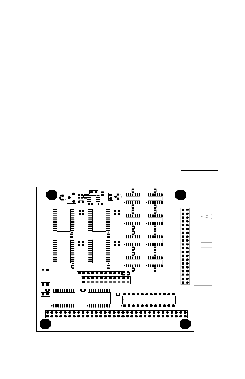
DESCRIPTION
6
The MSI-P460 Analog Output Card is an 8-bit stack-
through PC/104 card which reqyuires +5V and ±12V from
the PC/104 bus. It provides thirty-two analog output
channels with an output resolution of 8 bits. The card uses
four Analog Devices AD7228A analog-to-digital converters
with unity gain buffer amplifiers for the outputs. The
output ranges are selectable as either 0-5V or 0-10V with
a single hardware jumper. The card uses 16-bit I/O
mapped addressing which is jumper selectable. Outputs
are provided via a 40-pin AMP type 103311-8 connector.
The card outline is shown in Figure 1.
A. Card Addressing
The I/O-mapped card address is set by installing
appropriate jumpers on JP1, pins 1 thru 22. An
jumper for a given address bit sets the bit to 1 (true) and
uninstalled
C4
C2
C1
C3
A B
+
-
+
+
+
U1
1
A
R4
R3
C1
C15 R1
C18
C35
C8
C37
C14
C13
S1
JP1
C5
U2
10
U17
U4
U6
R2
C7
5
MSI-P460
C20
+
C17
U18
U16
C7
U5
MICROCOMPUTER SYSTEMS, INC.
C19
C36
C22
C10
C21
C24
C9
C38
C40
C23
C26
C39
R5
R6
A6
A5
C6
U3
15
BATON ROUGE, LA
20
C25
U8
U9
U10
U11
C28
C27
C30
C32
C31
C34
C33
25
U12
U13
U14
U15
J2
1
9
17
25
33
39
32
30
Figure 1. Outline of MSI-P460 Card.
Page MSI-P460 User Manual
1
Page 3

installed jumper sets the bit to 0 (false). Addresses A5
an
thru A15 are jumper selectable for defining the base
address of the card from 0000H to FFE0H on integral 20H
boundaries, where H denotes a hexadecimal number. To
assign a base address of 300H, for example, install all
jumpers except JP1-15,16 (A8) and JP1-13,14 (A9).
Individual channels have output addresses as given in
Table 1.
Table 1. I/O Addresses of MSI-P460.
Channel I/O Address * Channel I/O Address *
OUT 0 base address OUT 16 base address + 10
OUT 1 base address+1 OUT 17 base address + 11
OUT 2 base address+2 OUT 18 base address + 12
OUT 3 base address+3 OUT 19 base address + 13
OUT 4 base address+4 OUT 20 base address + 14
OUT 5 base address+5 OUT 21 base address + 15
OUT 6 base address+6 OUT 22 base address + 16
OUT 7 base address+7 OUT 23 base address + 17
OUT 8 base address+8 OUT 24 base address + 18
OUT 9 base address+9 OUT 25 base address + 19
OUT 10 base address+A OUT 26 base address + 1A
OUT 11 base address+B OUT 27 base address + 1B
OUT 12 base address+C OUT 28 base address + 1C
OUT 13 base address+D OUT 29 base address + 1D
OUT 14 base address+E OUT 30 base address + 1E
OUT 15 base address+F OUT 31 base address + 1F
* Offsets from the base address are in hexadecimal notation.
B. Output Range Selection
The output range is selected is determined by Jumper A.
An uninstalled jumper sets the output range for 4 to 6 V
and an installed jumper sets the output range for 8 to 10V,
respectively.
Potentiometer R2 must be adjusted to select the desired
Page MSI-P460 User Manual
2
Page 4

output voltage for the range selected (e.g., for a value 5V in
the range of 4 to 6V). This is performed by writing a FF to
an output channel (see next section on Programming) and
adjusting R2 for the desired output value. This sets the
span or maximum output value of all channels.
C. Programming the Outputs
Output programming is very simple. An I/O write of a byte
value to the channel address given in Table 1 will latch the
value into the output of the selected channel. The output
byte has a value from 0 to FF in hexadecimal. A value of 0
produces an output voltage of 0V. An output value of FF
produces an output equal to the range or span value
selected. In general, the output is
Output Value = (Output Data/256)*Span
D. Output Connector
The output connections to the output connector J2 are
given in Table 2.
Table 2. Outputs of Connector J2.
Channel J2 Pin No.* Channel J2 Pin No.*
OUT 0 1 OUT 16 21
OUT 1 2 OUT 17 22
OUT 2 3 OUT 18 23
OUT 3 4 OUT 19 24
OUT 4 5 OUT 20 25
OUT 5 6 OUT 21 26
OUT 6 7 OUT 22 27
OUT 7 8 OUT 23 28
OUT 8 11 OUT 24 31
OUT 9 12 OUT 25 32
OUT 10 13 OUT 26 33
OUT 11 14 OUT 27 34
Page MSI-P460 User Manual
3
Page 5

OUT 12 15 OUT 28 35
OUT 13 16 OUT 26 36
OUT 14 17 OUT 27 37
OUT 15 18 OUT 28 38
Note: Pins 9, 10, 19, 20, 29, 30, 39 and 40 are commons
for channels 0 thru 31.
E. Schematic Diagram
Page MSI-P460 User Manual
4
 Loading...