

Page 1

i
MSI-5149
Pentium TR10
Mainboard
Version 2.41
Intel and Pentium are registered trademarks of Intel Corporation.
PS/2 and OS/2 are registered trademarks of IBM Corporation.
Windows 95 and Windows NT are registered trademarks of Microsoft.
Netware is a registered trademark of Novell.
AMI is a registered trademark of American Megatrends Inc.
Award is a registered trademark of Award Software Inc.
AMD is a registered trademark of AMD.
Cyrix is a registered trademark of Cyrix.
Other brand, product names and trademarks are the properties of their respective
owners.
Page 2

ii
Manual Rev: 2.41
Release Date: September, 1997
FCC-B Radio Frequency Interference Statement
This equipment has been tested and found to comply with the limits for a
class B digital device, pursuant to part 15 of the FCC rules. These limits are
designed to provide reasonable protection against harmful interference when
the equipment is operated in a commercial environment. This equipment
generates, uses and can radiate radio frequency energy and, if not installed
and used in accordance with the instruction manual, may cause harmful
interference to radio communications. Operation of this equipment in a
residential area is likely to cause harmful interference, in which case the
user will be required to correct the interference at his own expense.
Notice 1
The changes or modifications not expressly approved by the party
responsible for compliance could void the user's authority to operate the
equipment.
Notice 2
Shielded interface cables and A.C. power cord, if any, must be used in order
to comply with the emission limits.
VOIR LA NOTICE D'INSTALLATION AVANT DE RACCORDER
AU RESEAU.
Page 3

iii
Edition
September 1997
Copyright Notice
This manual is copyrighted. No guarantee is given as to the
correctness of its contents. We reserve the right to make changes
without notification.
Trademarks
All trademarks used in this manual are the property of their respective
owners.
Page 4

iv
Table of Contents
Chapter 1: Introduction
System Board Features ----------------------------------------------- 1-2
System Board Layout-------------------------------------------------- 1-3
Chapter 2: Hardware Installation
Central Processing Unit: CPU--------------------------------------- 2-1
CPU Installation Procedure------------------------------------- 2-1
CPU Voltage Setting : JV1 - JV4, JV5------------------------ 2-3
CPU Speed and Voltage Setting:: SW1 & JV1-JV4, JV5 -- 2-4
CPU Fan Power Connector: JFAN----------------------------- 2-8
CMOS RAM Clear: JRTC-------------------------------------- 2-9
Memory Installation--------------------------------------------------- 2-10
Memory Bank Configuration----------------------------------- 2-10
Memory Installation Procedures--------------------------------- 2-11
Case Connector (JFP)------------------------------------------------- 2-15
Power Saving Switch Connector: JGS1----------------------------- 2-17
Power Saving LED Connector: JGL1------------------------------- 2-17
Serial Port Connectors: COM1 & COM2------------------------- 2-18
Parallel Port Connector: LPT-------------------------------------- 2-19
Floppy Disk Connector: FDD--------------------------------------- 2-20
Page 5

v
Hard Disk Connectors: IDE1 & IDE2------------------------------ 2-21
Power Supply Connector: JPW1------------------------------------- 2-22
Keyboard Connector: ATKBD--------------------------------------- 2-23
Mouse Connector: JM1----------------------------------------------- 2-24
IrDA Infrared Module Connector: IR------------------------------- 2-25
USB Connector: USB (Reserved)----------------------------------- 2-25
Chapter 3 AMI BIOS USER’S GUIDE
Entering BIOS Setup-------------------------------------------------- 3-2
Standard CMOS Setup------------------------------------------------ 3-4
Advanced CMOS Setup----------------------------------------------- 3-5
Advanced Chipset Setup---------------------------------------------- 3-9
Power Management Setup-------------------------------------------- 3-11
PCI/Plug and Play Setup---------------------------------------------- 3-14
Peripheral Setup-------------------------------------------------------- 3-17
Chapter 4 AWARD BIOS USER’S GUIDE
Entering Setup --------------------------------------------------------- 4-2
The Main Menu ------------------------------------------------------- 4-3
Standard CMOS Setup------------------------------------------------ 4-4
BIOS Features Setup -------------------------------------------------- 4-5
Page 6

vi
Chipset Features Setup ----------------------------------------------- 4-8
Power Management Setup ------------------------------------------- 4-9
PNP/PCI Configuration ---------------------------------------------- 4-11
Load Setup Defaults -------------------------------------------------- 4-12
Integrated Peripherals------------------------------------------------- 4-13
Supervisor/User Password Setting----------------------------------- 4-15
IDE HDD Auto Detection-------------------------------------------- 4-16
Page 7

CHAPTER 1 INTRODUCTION
Chapter 1
Introduction
The MS-5149 is a high-performance personal computer mainboard. This
mainboard supports Intel® Pentium® processors/Pentium® processor with
MMX™ technology , Cyrix® 6x86/6x86L/6x86MX processors and AMD® K5/
K6 processors.The system board supports the Peripheral Component
Interconnect (PCI) Local Bus standard and provides four 32-bit PCI bus
master slots.
It has a cache subsytem that can be configured for 256K or 512 K cache
memory to improve overall throughput.
The system board uses the highly integrated Intel® 83430VX Chipset to
support the PCI/ISA and Green standards, and to provide the Host/PCI
bridge. The Intel® 82430VX chipset integrates all system control functions.
1-1
Page 8

CHAPTER 1 INTRODUCTION
1.1 System Board Features
CPU
l Socket 7 supports Intel
®
Pentium® processors and Pentium® processor
with MMXTM technology
l The Cyrix
®
6x86/6x86L/6x86MX and AMD® K5/K6 processors are also
supported.
Chip Set
l Intel
®
82430 VX chip set.
Cache Memory
l Supports 256K/512K pipelined burst cache memory.
l Supports Directed Map Organization and Write-Back cache policy .
Main Memory
l Supports four memory banks using four 72-pin SIMM sockets and two
168-pin DIMM sockets.
l Up to 128 Mbytes main memory.
l Supports EDO Hyper Page Mode DRAM or Standard Fast Page mode
DRAM and SDRAM
Slots
l Four 32-bit Master PCI Bus slots and three 16-bit ISA bus slots wherein
one shared slot that can be used as ISA or PCI.
On-Board Peripherals
l On-Board Peripherals include:
- 1 floppy port supports 2FDD
- 2 serial ports (COMA + COMB)
- 1 parallel port supports ECP or EPP mode
- 2 PCI Bus Master IDE ports (up to four IDE HDD)
- USB (reserved)
Dimensions
l Baby-AT
®
form factor
l 26cm(L) x 22cm(W) x 4 layer PCB
Mounting
l 5 mounting holes
1-2
Page 9
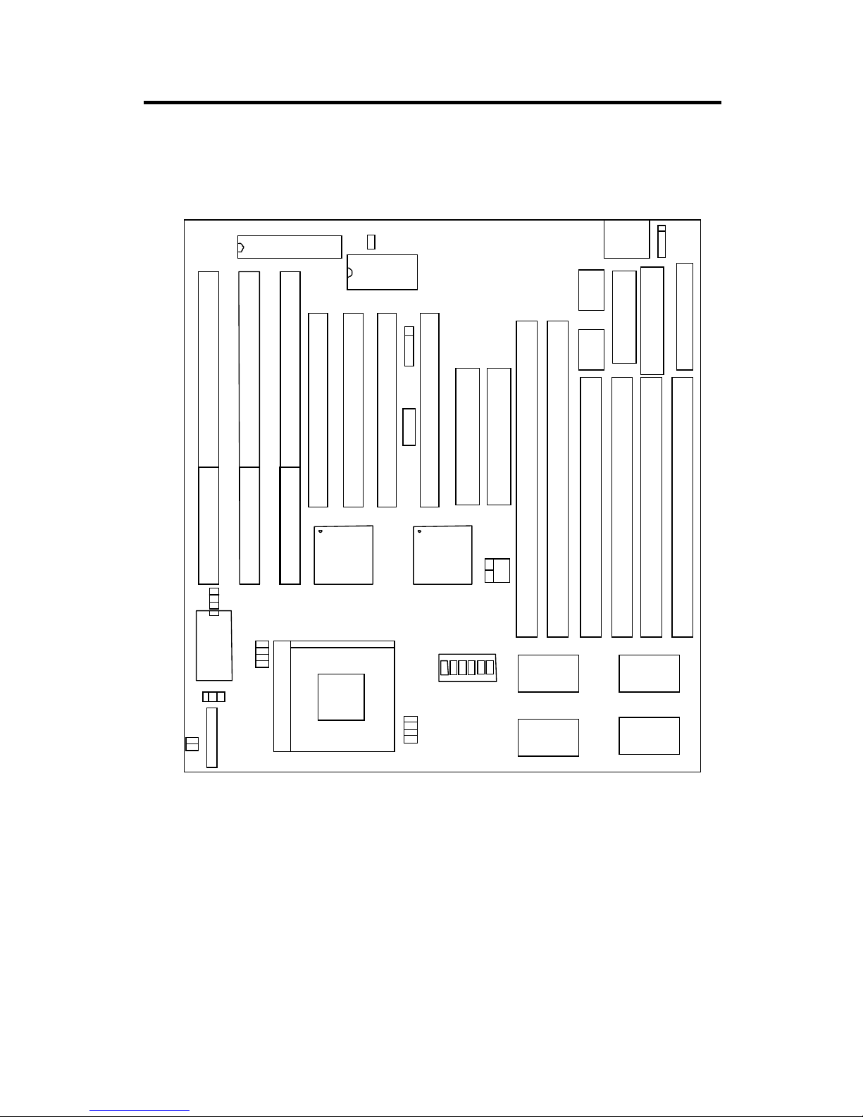
CHAPTER 1 INTRODUCTION
1.3 System Board Layout
1-3
SIMM1
FDD
PRN
COM1
DIMM2
DIMM1
HDD1
HDD2
437VX
JFAN
371SB
+ -
438VX
SRAM
438VX
SRAM
KBC
RTC
ATKBD
ISA 3
USB1
IR
JRTC1
+5V +3V
J2
JGL 1
JGS1
JFM1
JM1
SOCKET 7
ON
DIP
121
3
415
6
1
BIOS
SIMM2
SIMM3
SIMM4
COM2
Power Connector
JP1
JV1
JV2
JV3
JV4
1
SW1
ISA 2
ISA 1
PCI 3
PCI 4
PCI 2
PCI 1
JV5
MS-5149
Page 10
CHAPTER 2 HARDWARE INSTALLATION
Chapter 2
Hardware Installation
2.1 Central Processing Unit: CPU
The MS-5149 motherboard operates with Intel® Pentium® processors/
Pentium® processor with MMX technology, Cyrix® 6x86/6x86L/6x86MX,
and AMD® 5K86/K6 processors. It could operate with 2.8V to 3.52V
processors. The motherboard provides a 321-pin ZIF Socket 7 for easy CPU
installation, a DIP switch (SW1) to set the proper speed for the CPU and a
Jumper block (JV1 - JV4, JV5) for setting the CPU voltage. The CPU should
always have a cooling fan attached to prevent overheating.
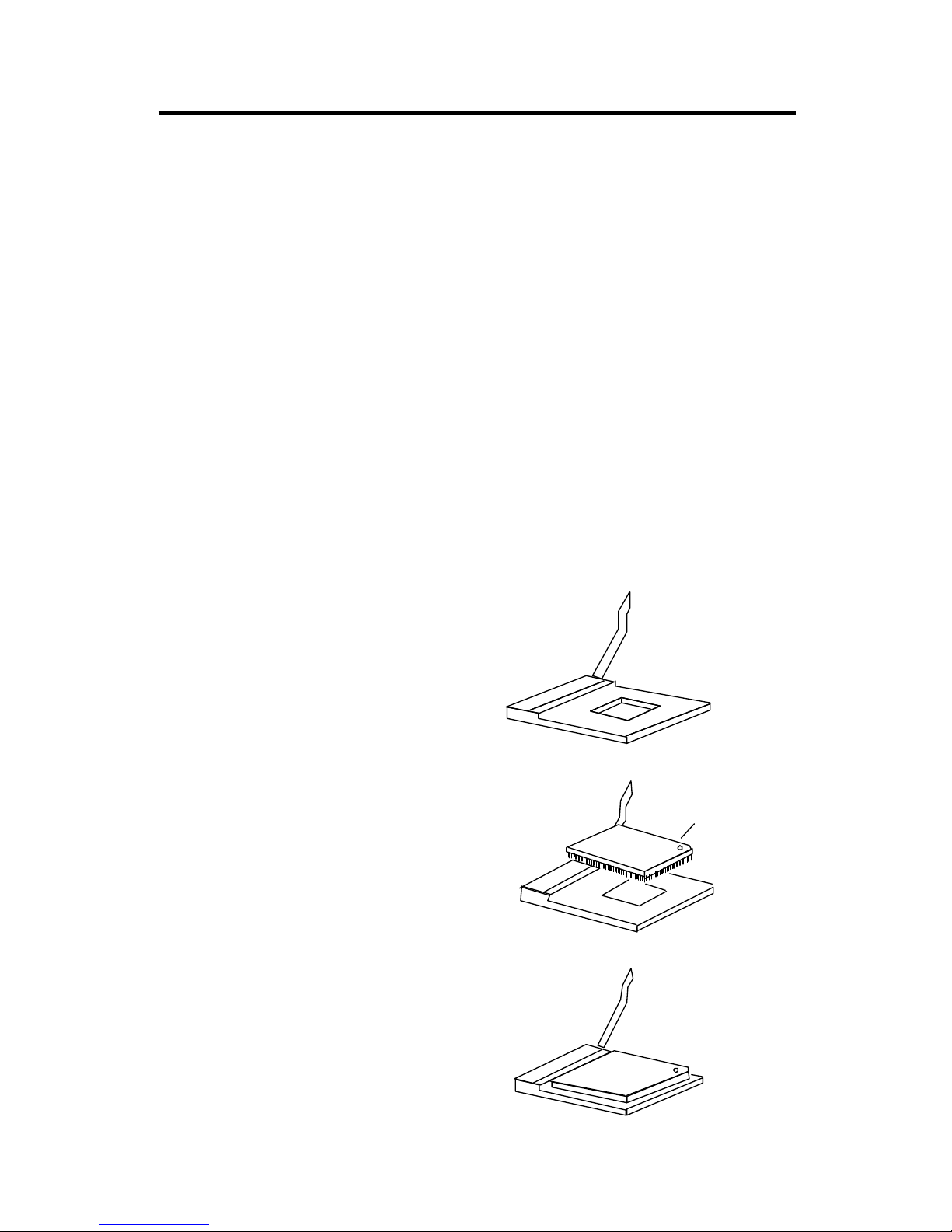
2.1-1 CPU Installation Procedure
1 . Pull the lever sideways away
from the socket. Then raise
the lever up to a 90-degree
angle.
3. Press the lever down to
complete the installation.
2 . Locate Pin 1 in the socket
and look for the white dot or
cut edge in the CPU. Match
Pin 1 with the white dot/cut
edge. Then insert the CPU.
It should insert easily.
CPU
CPU
Open Lever
Pin 1
Sliding
Plate
White dot/
Cut edge
Close
Lever
2-1
Page 11

CHAPTER 2 HARDWARE INSTALLATION
1. The 4 CPU clock frequencies that the system supports are 50 MHz,
55MHz, 60MHz and 66.6MHz (To adjust SW1 pin 1, 2 , and 3). See the
following chart to set the different Host Clock Frequencies.
1 2 3 CLOCK
ON ON OFF 50MHz
OFF O N OFF 55MHz
ON OFF OFF 60MHz
OFF OFF OFF 66.6MHz
SW1 CPU
2 . The DIP Switch SW1 (4, 5 and 6) is used to set the Core/Bus (Fraction)
ratio of the CPU. The actual core speed of the CPU is the Host Clock
Frequency multiplied by the Core/Bus ratio. For example:
If CPU Clock = 66.6MHz
Core/Bus ratio = 3/ 2
then CPU core speed = Host Clock x Core/Bus ratio
= 66.6MHz x 3/2
= 100MHz
3. The PCI Bus Clock is the CPU Clock Frequency divided by 2.
2.1-2 CPU Core Speed Derivation Procedure
2-2
4 5 6 Core/Bus Ratio
OFF OFF OFF 1.5
ON OFF OFF 2
ON ON OFF 2.5
OFF ON OFF 3
OFF ON OFF 3
OFF OFF OFF 3.5
SW1
CPU
Shaded Part are used by Intel® Pentium® processor
with MMXTM technology and AMD® K6
Note:
Page 12
CHAPTER 2 HARDWARE INSTALLATION
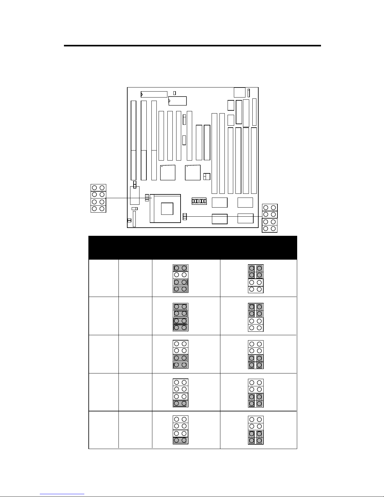
2.1-3 CPU Voltage Setting: JV1 - JV4, JV5
JV1~JV4VcoreV I/O
3.3 3.3
3.5
3.5
3.3
3.2
SIMM1
FDD
PRN
COM1
DIMM2
DIMM1
HDD1
HDD2
437VX
JFAN
371SB
+ -
438VX
SRAM
438VX
SRAM
KBC
RTC
ATKBD
ISA 3
USB1
IR
JRTC1
+5V +3V
J2
JGL 1
JGS1
JFM1
JM1
SOCKET 7
ON
DIP
121
3
4
1
5
6
1
BIOS
SIMM2
SIMM3
SIMM4
COM2
Power Connector
JP1
JV1
JV2
JV3
JV4
JV5
SW1
ISA 2
ISA 1
PCI 3
PCI 4
PCI 2
PCI 1
JV1
JV2
JV3
JV4
JV5
JV5
3.3
2.8
3.3 2.9
JV1
JV2
JV3
JV4
JV1
JV2
JV3
JV4
JV1
JV2
JV3
JV4
JV1
JV2
JV3
JV4
2-3
12
7
8
1
2
78
12
7
8
1
2
7
8
1
2
7
8
JV1
JV2
JV3
JV4
Page 13
CHAPTER 2 HARDWARE INSTALLATION
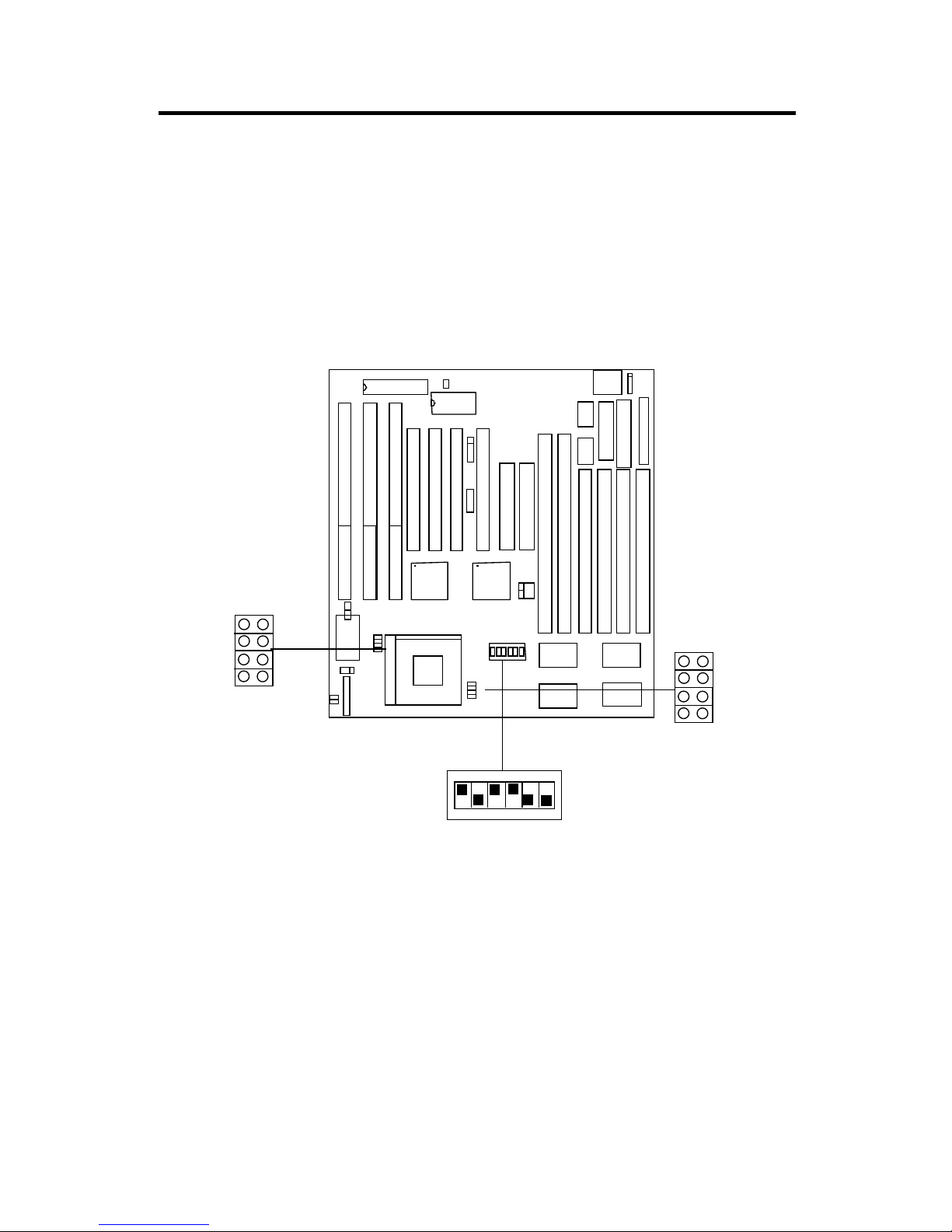
2.1-3 CPU Speed and Voltage Setting: SW1 & JV1-JV4, JV5
To adjust the speed and voltage of the CPU, you must know the specification of your CPU (always ask the vendor for CPU specificaton). Then refer
to Table 2.1 (Intel® processors), T able 2.2 (Cyrix® processors) and T able
2.3 (AMD® processors) for proper setting.
SW1
1 2 3 4 5 6
ON
ON
OFF
Speed Setting
SIMM1
FDD
PRN
COM1
DIMM2
DIMM1
HDD1
HDD2
437VX
JFAN
371SB
+ -
438VX
SRAM
438VX
SRAM
KBC
RTC
ATKBD
ISA 3
USB1
IR
JRTC1
+5V +3V
J2
JGL 1
JGS1
JFM1
JM1
SOCKET 7
ON
DIP
121
3
4
1
5
6
1
BIOS
SIMM2
SIMM3
SIMM4
COM2
Power Connector
JP1
JV1
JV2
JV3
JV4
JV5
SW1
ISA 2
ISA 1
PCI 3
PCI 4
PCI 2
PCI 1
JV1
JV2
JV3
JV4
JV5
2-4
Page 14
CHAPTER 2 HARDWARE INSTALLATION
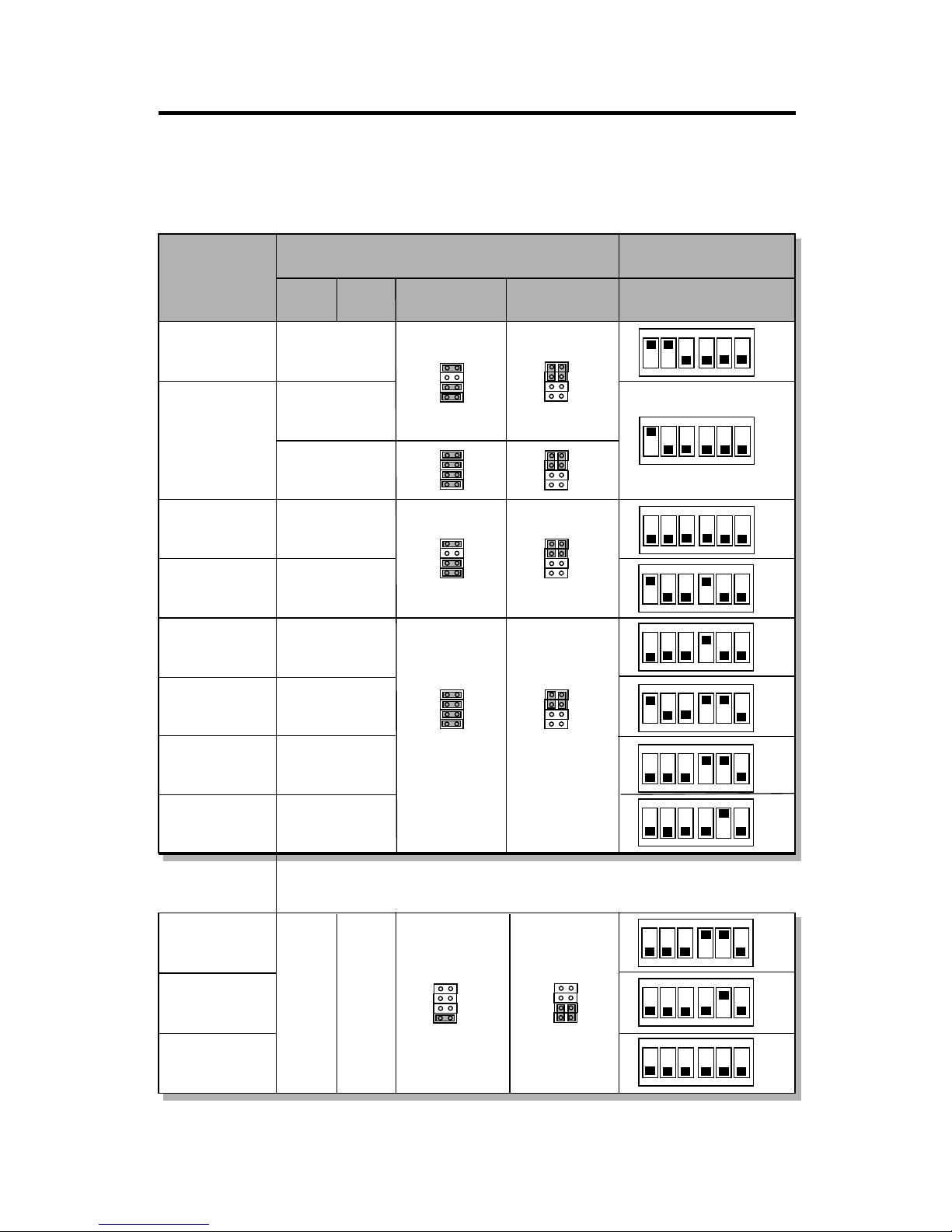
Table 2.1 Intel® Pentium® processors
ON DIP
123 456
ON
OFF
90MHz
100MHz
120MHz
133MHz
150MHz
166MHz
200MHz
3.3
3.5
3.5
3.3
3.3
3.5
3.5
ON DIP
123 456
ON
OFF
ON DIP
123 456
ON
OFF
ON DIP
123 456
ON
OFF
ON DIP
123 456
ON
OFF
ON DIP
123 456
ON
OFF
75MHz
3.3
CPU Type
CPU SpeedCPU Voltage
SW1
JV1~JV4
VI/O Vcore
JV5
2-5
12
7
8
12
78
12
78
12
78
JV1
JV2
JV3
JV4
JV1
JV2
JV3
JV4
JV1
JV2
JV3
JV4
JV1
JV2
JV3
JV4
ON DIP
123 456
ON
OFF
166MHz
200MHz
233MHz
3.5
ON DIP
123 456
ON
OFF
3.3
2.8
12
78
ON DIP
123 456
ON
OFF
ON DIP
123 456
ON
OFF
JV1
JV2
JV3
JV4
ON DIP
123 456
ON
OFF
a. Intel® Pentium
®
processors
b. Intel® Pentium
®
processors with MMXTM technology
Page 15

CHAPTER 2 HARDWARE INSTALLATION
Table 2.2 Cyrix® 6x86 processor
Cyrix® processor uses PR to rate the speed of their processors based on
Intel® processor core speed. For example P120+ (100MHz) has 120MHz core
speed of an Intel® processor but has 100MHz core speed in Cyrix® processor .
Cyrix® processor should always uses a more powerful fan (ask vendor for
proper cooling fan).
ON DIP
123 456
ON
OFF
3.5
ON DIP
123 456
ON
OFF
ON DIP
123 456
ON
OFF
P120+
(100MHz)
CPU Type
CPU SpeedCPU Voltage
SW1
JV1~JV4
VI/O Vcore
P133+
(110MHz)
P150+
(120MHz)
P166+
(133MHz)
ON DIP
123 456
ON
OFF
JV5
Cyrix® 6x86L processor
3.3
PR166
(166MHz)
ON DIP
123 456
ON
OFF
2.8
2-6
12
78
12
78
JV1
JV2
JV3
JV4
JV1
JV2
JV3
JV4
Cyrix® 6x86MX processor
3.3
PR166
2.9
12
78
JV1
JV2
JV3
JV4
*PR200
*PR233
ON DIP
123 456
ON
OFF
ON DIP
123 456
ON
OFF
ON DIP
123 456
ON
OFF
Note: * This CPU type is reserved for future support.
Page 16
CHAPTER 2 HARDWARE INSTALLATION
Table 2.3 AMD® K5 processor
AMD® K5 processor uses PR to rate the speed of their processors based on
Intel® processor core speed. For example: P133+ (100MHz) has 133MHz core
speed of Intel® processor but has 100MHz core speed in AMD® processor.
AMD® processor should always uses a more powerful fan (ask vendor for
proper cooling fan).
ON DIP
123 456
ON
OFF
3.5
ON DIP
123 456
ON
OFF
ON DIP
123 456
ON
OFF
CPU Type
CPU SpeedCPU Voltage
SW1JV1~JV4VI/O Vcore
PR90
(90MHz)
PR100
(100MHz)
PR133
(133MHz)
ON DIP
123 456
ON
OFF
PR166
(166MHz)
JV5
AMD® K6 processor
3.3
PR166
(166MHz)
ON DIP
123 456
ON
OFF
PR200
(200MHz)
2.9
2-7
ON DIP
123 456
ON
OFF
12
78
12
78
JV1
JV2
JV3
JV4
JV1
JV2
JV3
JV4
Page 17

CHAPTER 2 HARDWARE INSTALLATION
2.1-4 CPU Fan Power Connector: JFAN
This connector supports CPU cooling fan with +12V. It supports both two
and three pin head connector. When connecting the wire to the connector,
always take note that the red wire is the positive and should be connected to
the +12V .
JFAN
Connector
+12V
GND
GND
Recommended CPU cooling fan specification:
- Metallic Clip
- RPM 5000
- CFM 10
- +12V
- 52x52x10mm
- Ball Bearing
Note: Always consult vendor for
proper CPU cooling fan.
2-8
SIMM1
FDD
PRN
COM1
DIMM2
DIMM1
HDD1
HDD2
437VX
JFAN
371SB
+ -
438VX
SRAM
438VX
SRAM
KBC
RTC
ATKBD
ISA 3
USB1
IR
JRTC1
+5V +3V
J2
JGL 1
JGS1
JFM1
JM1
SOCKET 7
ON
DIP
121
3
4
1
5
6
1
BIOS
SIMM2
SIMM3
SIMM4
COM2
Power Connector
JP1
JV1
JV2
JV3
JV4
1
SW1
ISA 2
ISA 1
PCI 3
PCI 4
PCI 2
PCI 1
JV5
Page 18
CHAPTER 2 HARDWARE INSTALLATION
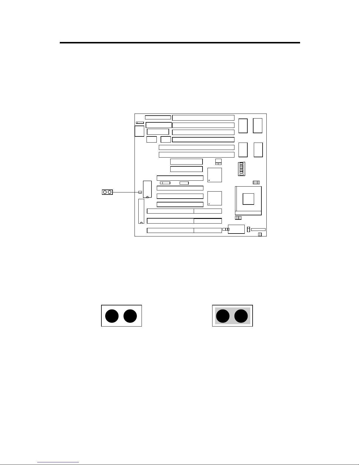
2.1-5 CMOS RAM Clear: JRTC
This jumper is for clearing the R TC data.
JRTC
keep Data
(default)
clear
SIMM1
FDD
PRN
COM1
DIMM2
DIMM1
HDD1
HDD2
437VX
JFAN
371SB
+ -
438VX
SRAM
438VX
SRAM
KBC
RTC
ATKBD
ISA 3
USB1
IR
JRTC1
+5V +3V
J2
JGL 1
JGS1
JFM1
JM1
SOCKET 7
ON
DIP
121
3
4
1
5
6
1
BIOS
SIMM2
SIMM3
SIMM4
COM2
Power Connector
JP1
JV1
JV2
JV3
JV4
JV5
SW1
ISA 2
ISA 1
PCI 3
PCI 4
PCI 2
PCI 1
2-9
Page 19
CHAPTER 2 HARDWARE INSTALLATION
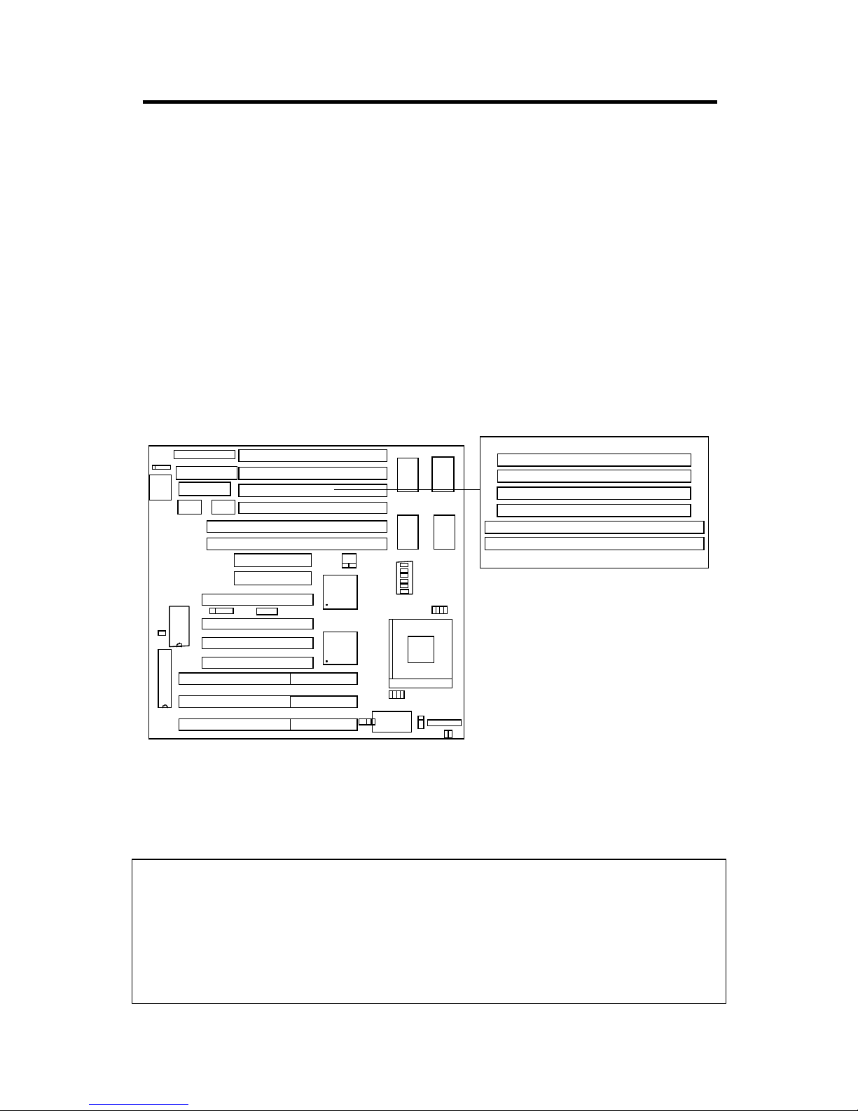
2.2 Memory Installation
2.2-1 Memory Bank Configuration
The system board supports a maximum of 128M of memory . It provides four
72-pin SIMMs (Single In-Line Memory Module) and two 168-pin DIMM
sockets. This board supports 4 banks wherein each bank supports memory
ranging from 4MB to 32MB. A Bank always has a pair of SIMM or a single
DIMM. Each bank supports 4M, 8M, 16M and 32M. The 2MB is the
minimum and the 16MB is the maximum for one 72-pin single sided memory
module.
W arning! SIMM Socket 1-4 power level is 5 volts. DIMM Socket 1 & 2
power level is 3.3 V/5V. W e suggest not to install both the SIMM
& DIMM at the same time. But if you want to install both SIMM
& DIMM slot, you must use a 3.3 volt DIMM with 5 volt I/O
signal tolerance or use a full 5 volt DIMM module. Otherwise it
may cause damage to the DIMM.
SIMM4(Bank 2/3) RAS2+ RAS3
SIMM3(Bank 2/3) RAS2+ RAS3
SIMM2(Bank 0/1) RAS0+ RAS1
SIMM1(Bank 0/1) RAS0+ RAS1
DIMM2(Bank 0/1) RAS1+ RAS0
DIMM1(Bank 2/3) RAS3+ RAS2
SIMM1
FDD
PRN
COM1
DIMM2
DIMM1
HDD1
HDD2
437VX
JFAN
371SB
+ -
438VX
SRAM
438VX
SRAM
KBC
RTC
ATKBD
ISA 3
USB1
IR
JRTC1
+5V +3V
J2
JGL 1
JGS1
JFM1
JM1
SOCKET 7
ON
DIP
121
3
4
1
5
6
1
BIOS
SIMM2
SIMM3
SIMM4
COM2
Power Connector
JP1
JV1
JV2
JV3
JV4
JV5
SW1
ISA 2
ISA 1
PCI 3
PCI 4
PCI 2
PCI 1
2-10
Page 20
CHAPTER 2 HARDWARE INSTALLATION
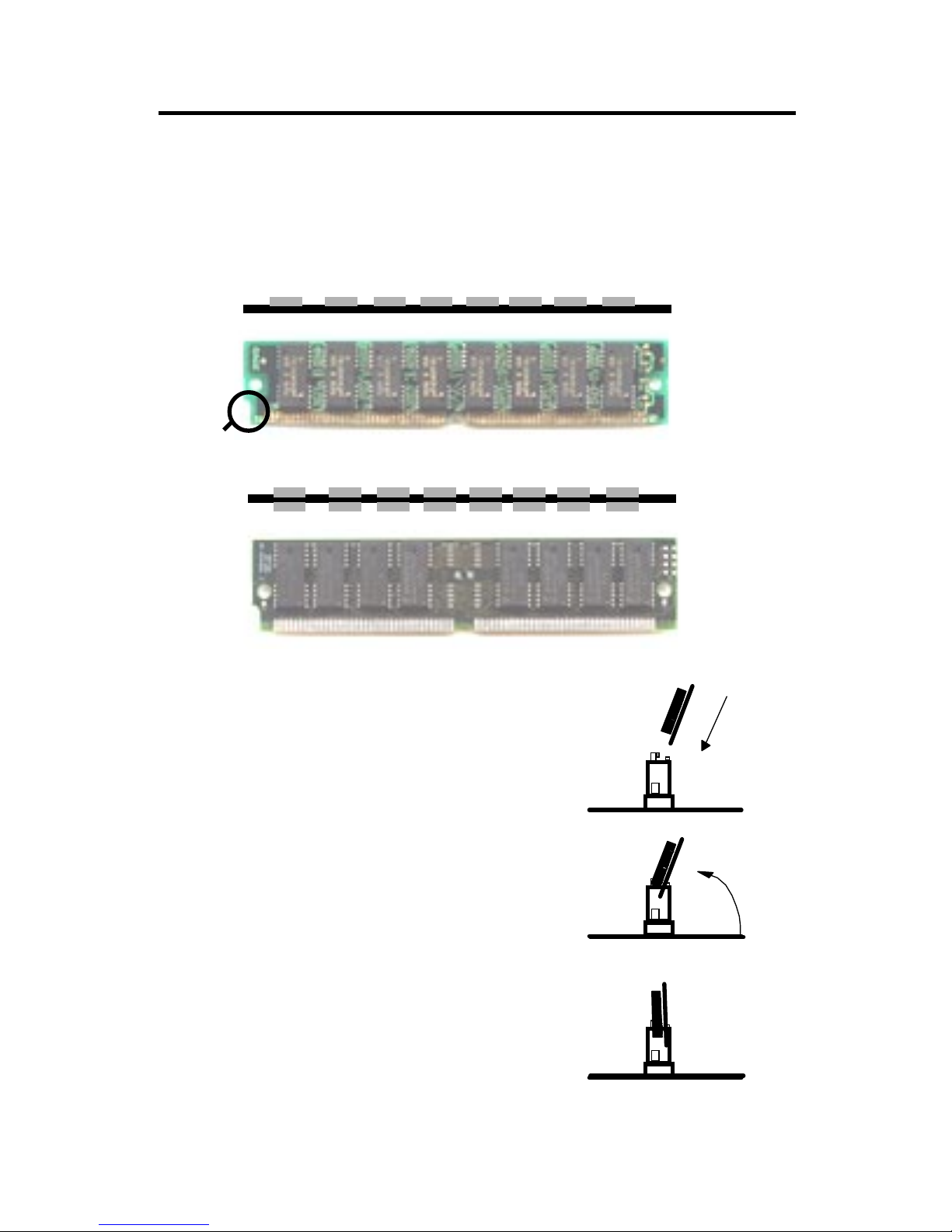
2.2-2 Memory Installation Procedures:
1. The SIMM slot has a “Plastic Safety
Tab” and the SIMM memory module
has a “Notched End”, so the SIMM
memory module can only fit in one
direction.
2. Insert the SIMM memory modules into
the socket at 45-degree angle. Then
push into a vertical position so that it
will snap into place.
3. The Mounting Holes and Metal Clips
should fit over the edge and hold the
SIMM memory modules in place.
A. How to install a SIMM Module
Single Sided SIMM
Double Sided SIMM
Note: Always use a 5 volts SIMM with 70 ns
or above(Fast Page or EDO)
Notched
End
2-11
Page 21
CHAPTER 2 HARDWARE INSTALLATION
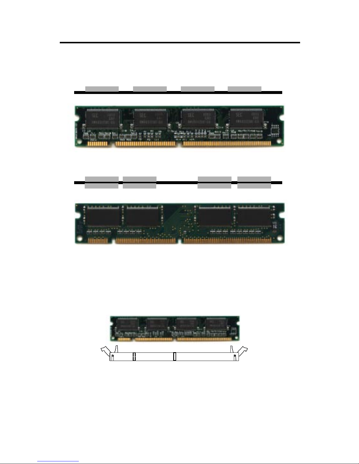
B. How to install a DIMM Module
1. The DIMM slot has a two key mark “VOLT and DRAM” , so the
DIMM memory module can only fit in one direction.
2. Insert the DIMM memory module vertically into the DIMM slot.
Then, push it in.
3. Close the plastic clip at the side of the DIMM slot.
Single Sided DIMM
Double Sided DIMM
2-12
Note: If you have installed SIMM and DIMM at the same time, you must
use a 3.3 volt DIMM with 5 volt I/O signal tolerance or a full 5 volt
DIMM module (EDO, FP or SDRAM). Look for J2 to select the
DIMM voltage.
Page 22

CHAPTER 2 HARDWARE INSTALLATION
A.1 DIMM Power V oltage Selector : J2
J2
J2
DIMM Voltage J2
5V
3.3V
DIMM Power Level : 3.3V or 5V
SIMM Power Level : Fixed at 5V
SIMM1
FDD
PRN
COM1
DIMM2
DIMM1
HDD1
HDD2
437VX
JFAN
371SB
+ -
438VX
SRAM
438VX
SRAM
KBC
RTC
ATKBD
ISA 3
USB1
IR
JRTC1
+5V +3V
J2
JGL 1
JGS1
JFM1
JM1
SOCKET 7
ON
DIP
121
3
4
1
5
6
1
BIOS
SIMM2
SIMM3
SIMM4
COM2
Power Connector
JP1
JV1
JV2
JV3
JV4
1
SW1
ISA 2
ISA 1
PCI 3
PCI 4
PCI 2
PCI 1
JV5
+5V +3V
+5V +3V
J2
+5V +3V
2-13
Page 23

CHAPTER 2 HARDWARE INSTALLATION
1. Make sure that the SIMM banks are using the same type and equal size
density memory.
2 . T o operate properly , at least two 72-pin SIMM module must be installed in
the same bank or one 168-pin DIMM module must be installed. The
system cannot operate with only one 72-pin SIMM module.
3. This mainboard supports Table Free memory so memory can be installed
on Bank 0 (SIMM1 + SIMM2), Bank 1 (SIMM3 + SIMM4), Bank 2
(DIMM1) or Bank3 (DIMM 2) in any order.
S--SS--
SD-D- -DS -DD --
-S--
--S-
-D--
--D-
---S
--SS
---D
--DD
S--S
SS-S
D-SD-DDSS-
-S-S
-SSS
-SSD
-D-S
-D-D
SIMM1 + SIMM2
Bank0 + Bank1
SIMM3+ SIMM4
Bank2 +Bank3
DIMM1
Bank2+Bank3
DIMM2
Bank0+Bank1
S = Single D = Double Shaded = See Warning
2.2-3 Memory Population Rule
2-14
Page 24

CHAPTER 2 HARDWARE INSTALLATION
2.3 Case Connector : JFP
The Turbo LED, Turbo Switch, Hardware Reset, Key Lock, Power LED,
Power Saving LED, Sleep Switch, Speaker and HDD LED are all connected to
the JFP connector block.
1
JFP
10
21
1
x
x
1122
21
Speaker
Power LED
Keylock
Turbo LED
Reset Switch
HDD LED
10
20
+
+
+
Turbo Switch
L H
Power
Saving
Switch
+
Power
Saving
LED
Figure 2.1
SIMM1
FDD
PRN
COM1
DIMM2
DIMM1
HDD1
HDD2
437VX
JFAN
371SB
+ -
438VX
SRAM
438VX
SRAM
KBC
RTC
ATKBD
ISA 3
USB1
IR
JRTC1
+5V +3V
J2
JGL 1
JGS1
JFM1
JM1
SOCKET 7
ON
DIP
121
3
4
1
5
6
1
BIOS
SIMM2
SIMM3
SIMM4
COM2
Power Connector
JP1
JV1
JV2
JV3
JV4
JV5
SW1
ISA 2
ISA 1
PCI 3
PCI 4
PCI 2
PCI 1
2-15
Page 25

CHAPTER 2 HARDWARE INSTALLATION
2-16
2.3-1 Turbo LED
The T urbo LED is used to monitor if the turbo switch is ON/OFF. You can
connect the Turbo LED from the system case to this pin. (See Figure 2.1)
2.3-2 Hardware Reset
Reset switch is used to reboot the system rather than turning the power ON/
OFF . A void rebooting while the HDD LED is lit. You can connect the Reset
switch from the system case to this pin. (See Figure 2.1)
2.3-3 Keylock
Keylock allows you to disable the keyboard for security purposes. You can
connect the keylock to this pin. (See Figure 2.1)
2.3-4 Power LED
The Power LED is always lit while the system power is on. You can connect
the Power LED from the system case to this pin. (See Figure 2.1)
2.3-5 Suspend Switch
The Turbo switch or Suspend switch allows the user to suspend the system
while not in use. It can be controlled by BIOS power management setup
switch function. You can connect the Turbo Switch from the system case to
this pin. (See Figure 2.1)
2.3-6 Speaker
Speaker from the system case is connected to this pin. (See Figure 2.1)
2.3-7 HDD LED
HDD LED shows the activity of a hard disk drive. Avoid turning the power
off while the HDD led is lit. You can connect the HDD LED from the system
case to this pin. (See Figure 2.1).
Page 26

CHAPTER 2 HARDWARE INSTALLATION
2.4 Power Saving Switch Connector: JGS1/
Power Saving LED Connector: JGL1
Attach a a power saving switch to this connector. When the switch is
pressed, the system immediately goes into suspend mode. Press any key
and the system wakes up.
JGS1
JGL1
SIMM1
FDD
PRN
COM1
DIMM2
DIMM1
HDD1
HDD2
437VX
JFAN
371SB
+ -
438VX
SRAM
438VX
SRAM
KBC
RTC
ATKBD
ISA 3
USB1
IR
JRTC1
+5V +3V
J2
JGL 1
JGS1
JFM1
JM1
SOCKET 7
ON
DIP
121
3
4
1
5
6
1
BIOS
SIMM2
SIMM3
SIMM4
COM2
Power Connector
JP1
JV1
JV2
JV3
JV4
JV5
SW1
ISA 2
ISA 1
PCI 3
PCI 4
PCI 2
PCI 1
2-17
Page 27

CHAPTER 2 HARDWARE INSTALLATION
2.5 Serial Port Connectors: COM1 & COM2
The system board has two connectors for serial ports COM1 and COM2.
These two ports are 16550A high speed communication ports that send/
receive 16 bytes FIFOs. You can attach a mouse or a modem cable directly
into these connectors.
SIMM1
FDD
PRN
COM1
DIMM2
DIMM1
HDD1
HDD2
437VX
JFAN
371SB
+ -
438VX
SRAM
438VX
SRAM
KBC
RTC
ATKBD
ISA 3
USB1
IR
JRTC1
+5V +3V
J2
JGL 1
JGS1
JFM1
JM1
SOCKET 7
ON
DIP
121
3
4
1
5
6
1
BIOS
SIMM2
SIMM3
SIMM4
COM2
Power Connector
JP1
JV1
JV2
JV3
JV4
JV5
SW1
ISA 2
ISA 1
PCI 3
PCI 4
PCI 2
PCI 1
COM2
COM1
2-18
Page 28

CHAPTER 2 HARDWARE INSTALLATION
2.6 Parallel Port Connector: LPT
The system board provides a connector for LPT. A parallel port is a
standard printer port that also supports Enhanced Parallel Port(EPP) and
Extended capabilities Parallel Port(ECP).
SIMM1
FDD
PRN
COM1
DIMM2
DIMM1
HDD1
HDD2
437VX
JFAN
371SB
+ -
438VX
SRAM
438VX
SRAM
KBC
RTC
ATKBD
ISA 3
USB1
IR
JRTC1
+5V +3V
J2
JGL 1
JGS1
JFM1
JM1
SOCKET 7
ON
DIP
121
3
4
1
5
6
1
BIOS
SIMM2
SIMM3
SIMM4
COM2
Power Connector
JP1
JV1
JV2
JV3
JV4
JV5
SW1
ISA 2
ISA 1
PCI 3
PCI 4
PCI 2
PCI 1
LPT
2-19
Page 29

CHAPTER 2 HARDWARE INSTALLATION
2.7 Floppy Disk Connector: FDD
The system board also provides a standard floppy disk connector FDD that
supports 360K, 720K, 1.2M, 1.44M and 2.88M floppy disk types. You can
attach a floppy disk cable directly to this connector.
FDD
1
SIMM1
FDD
PRN
COM1
DIMM2
DIMM1
HDD1
HDD2
437VX
JFAN
371SB
+ -
438VX
SRAM
438VX
SRAM
KBC
RTC
ATKBD
ISA 3
USB1
IR
JRTC1
+5V +3V
J2
JGL 1
JGS1
JFM1
JM1
SOCKET 7
ON
DIP
121
3
4
1
5
6
1
BIOS
SIMM2
SIMM3
SIMM4
COM2
Power Connector
JP1
JV1
JV2
JV3
JV4
JV5
SW1
ISA 2
ISA 1
PCI 3
PCI 4
PCI 2
PCI 1
2--20
Page 30

CHAPTER 2 HARDWARE INSTALLATION
2.8 Hard Disk Connectors: IDE1 & IDE2
The system board has a 32-bit Enhanced PCI IDE Controller that provides
for two HDD connectors IDE1 (primary) and IDE2 (secondary). Y ou can
connect up to four hard disk drives, CD-ROM, 120MB Floppy (reserved for
future BIOS) and other devices to IDE1 and IDE2.
Primary IDE Connector
Secondary IDE Connector
IDE1(primary IDE connector)
The first hard disk should always be connected to IDE1. IDE1 can connect a
Master and a Slave drive.
IDE2(secondary IDE connector)
IDE2 can connect a Master and a Slave drive.
1
1
SIMM1
FDD
PRN
COM1
DIMM2
DIMM1
HDD1
HDD2
437VX
JFAN
371SB
+ -
438VX
SRAM
438VX
SRAM
KBC
RTC
ATKBD
ISA 3
USB1
IR
JRTC1
+5V +3V
J2
JGL 1
JGS1
JFM1
JM1
SOCKET 7
ON
DIP
121
3
4
1
5
6
1
BIOS
SIMM2
SIMM3
SIMM4
COM2
Power Connector
JP1
JV1
JV2
JV3
JV4
JV5
SW1
ISA 2
ISA 1
PCI 3
PCI 4
PCI 2
PCI 1
2-21
Page 31

CHAPTER 2 HARDWARE INSTALLATION
2.9 Power Supply Connector: JPW1
JPW1 is a standard 12-pin AT® connector . Be sure to attach the
connectors with the two black wires at the center .
Power Connector
Pin Description Pin Description
1 Power Good 7 Ground
2 +5V DC 8 Ground
3 +12V DC 9 -5V DC
4 -12V DC 10 +5V DC
5 Ground 11 +5V DC
6 Ground 12 +5V DC
1
SIMM1
FDD
PRN
COM1
DIMM2
DIMM1
HDD1
HDD2
437VX
JFAN
371SB
+ -
438VX
SRAM
438VX
SRAM
KBC
RTC
ATKBD
ISA 3
USB1
IR
JRTC1
+5V +3V
J2
JGL 1
JGS1
JFM1
JM1
SOCKET 7
ON
DIP
121
3
4
1
5
6
1
BIOS
SIMM2
SIMM3
SIMM4
COM2
Power Connector
JP1
JV1
JV2
JV3
JV4
JV5
SW1
ISA 2
ISA 1
PCI 3
PCI 4
PCI 2
PCI 1
12
2-22
Page 32

CHAPTER 2 HARDWARE INSTALLATION
SIMM1
FDD
PRN
COM1
DIMM2
DIMM1
HDD1
HDD2
437VX
JFAN
371SB
+ -
438VX
SRAM
438VX
SRAM
KBC
RTC
ATKBD
ISA 3
USB1
IR
JRTC1
+5V +3V
J2
JGL 1
JGS1
JFM1
JM1
SOCKET 7
ON
DIP
121
3
4
1
5
6
1
BIOS
SIMM2
SIMM3
SIMM4
COM2
Power Connector
JP1
JV1
JV2
JV3
JV4
JV5
SW1
ISA 2
ISA 1
PCI 3
PCI 4
PCI 2
PCI 1
2.10 Keyboard Connector: ATKBD
The system board provides a standard AT® keyboard mini DIN connector
for attaching a keyboard. You can plug a keyboard cable directly to this
connector .
Keyboard
Connector
Pin1
NC
Pin2
VCC
Pin3
DATA
Pin4
GND
Pin5
CLK
2-23
Page 33

CHAPTER 2 HARDWARE INSTALLATION
SIMM1
FDD
PRN
COM1
DIMM2
DIMM1
HDD1
HDD2
437VX
JFAN
371SB
+ -
438VX
SRAM
438VX
SRAM
KBC
RTC
ATKBD
ISA 3
USB1
IR
JRTC1
+5V +3V
J2
JGL 1
JGS1
JFM1
JM1
SOCKET 7
ON
DIP
121
3
4
1
5
6
1
BIOS
SIMM2
SIMM3
SIMM4
COM2
Power Connector
JP1
JV1
JV2
JV3
JV4
JV5
SW1
ISA 2
ISA 1
PCI 3
PCI 4
PCI 2
PCI 1
2.11 Mouse Connector: JM1
The system board provides a 5-pin connector for PS/2® mouse cable
(optional). You can plug a PS/2® mouse to PS/2® mouse cable. The
connector location is shown below.
2-24
JM1
1
VCC
GND
CLK
DATA
Page 34

CHAPTER 2 HARDWARE INSTALLATION
SIMM1
FDD
PRN
COM1
DIMM2
DIMM1
HDD1
HDD2
437VX
JFAN
371SB
+ -
438VX
SRAM
438VX
SRAM
KBC
RTC
ATKBD
ISA 3
USB1
IR
JRTC1
+5V +3V
J2
JGL 1
JGS1
JFM1
JM1
SOCKET 7
ON
DIP
121
3
4
1
5
6
1
BIOS
SIMM2
SIMM3
SIMM4
COM2
Power Connector
JP1
JV1
JV2
JV3
JV4
JV5
SW1
ISA 2
ISA 1
PCI 3
PCI 4
PCI 2
PCI 1
2.12 IrDA Infrared Module Connector: IR
The system board provides a 5-pin infrared connector(IR) for IR module.
This connector is for optional wireless transmitting and receiving infrared
module. You must configure the setting through BIOS setup.
2.13 USB Connector: USB (Reserved)
This 10-pin connector supports USB devices. This function is a reserved
function.
IR
USB
GNDGNDD1+ D1-
VCC
VCC DO-DO+GND
GND
VCC NC RXGND TX
2-25
SIMM1
FDD
PRN
COM1
DIMM2
DIMM1
HDD1
HDD2
437VX
JFAN
371SB
+ -
438VX
SRAM
438VX
SRAM
KBC
RTC
ATKBD
ISA 3
USB1
IR
JRTC1
+5V +3V
J2
JGL 1
JGS1
JFM1
JM1
SOCKET 7
ON
DIP
121
3
4
1
5
6
1
BIOS
SIMM2
SIMM3
SIMM4
COM2
Power Connector
JP1
JV1
JV2
JV3
JV4
JV5
SW1
ISA 2
ISA 1
PCI 3
PCI 4
PCI 2
PCI 1
Page 35

Chapter 3 AMI® BIOS USER’S GUIDE
3-1
Chapter 3
AMI® BIOS USER GUIDE
The system configuration information and chipset register
information is stored in the CMOS RAM. This
information is retained by a battery when the power is off.
Enter the BIOS setup (if needed) to modify this
information.
Below is the description on how to enter BIOS setup , and
the meaning of each option.
Page 36

Chapter 3 AMI® BIOS USER’S GUIDE
3-2
3.1 Entering BIOS Setup
Enter the AMI® setup Program's Main Menu as follows:
1.Turn on or reboot the system. The following screen appears with a
series of diagnostic check
.
AMIBIOS (C) 1997 American Megatrends Inc.,
Hit <DEL> if you want to run setup
(C) American Megatrends Inc.,
51-XXXX-001169-00101111-071595-82430VX-F
2.When the "Hit <DEL>“ message appears, press <DEL> key to
enter the BIOS setup screen.
Note: If you don’t want to modify CMOS original setting, don’t press any key;
just wait for the system to boot up.
Page 37

Chapter 3 AMI® BIOS USER’S GUIDE
3-3
3. After pressing <DEL> key, the BIOS Setup screen (as below) will
display
.
AMIBIOS SETUP - BIOS SETUP UTILITIES
(C) 1997 American Megatrends, Inc. All Rights Reserved
Standard CMOS Setup
Advanced CMOS Setup
Advanced Chipset Setup
Power Management Setup
PCI / Plug and Play Setup
Peripheral Setup
Change User Password
Change Supervisor Password
Change Language Setting
Auto Configuration with Optimal Settings
Auto Configuration with Fail Safe Settings
Save Settings and Exit
Exit without Saving
Standard CMOS Setup for changing time,date, etc.
ESC : Exit : Sel F2/F3 : Color F10 : Save & Exit
4. Use the <> and <> key to move the highlight scroll up or down.
5. Use the <ENTER> key to choose the option.
6. To exit, press <ESC>. To save and exit, press <F10>.
7. Section 3-2 to 3-7 will describe the option in details.
Page 38

Chapter 3 AMI® BIOS USER’S GUIDE
3-4
3.2 STANDARD CMOS SETUP
1. Press <ENTER> on "Standard CMOS Setup" of MAIN MENU
SCREEN and the above screen appears.
AMIBIOS SETUP - STANDARD CMOS SETUP
(C)1997 American Megatrends, Inc. All Rights Reserved
Date (mm/dd/yyyy) : Wed, Mar 20, 1997
Time (hh/mm/ss) : 16:19:52
Floppy Drive A: 3 1/2 ,1.44M
Floppy Drive B: Not Installed
LBA BLK P10 32Bit
Type Size Cyin Head WPcom Sec Mode Mode Mode Mode
Pri Master : AUTO ON ON ON AUTO
Pri Slave : AUTO ON ON ON AUTO
Sec Master : AUTO ON ON ON AUTO
Sec Slave : AUTO ON ON ON AUTO
Month : Jan - Dec ESC:Exit :Sel
Day: 01 - 31 PgUp/PgDn:Modify
Year: 1901-2099 F2/F3:Color
2. Use <
> and <> to choose the item. Use <PgUp> and <PgDn> keys to
modify the highlighted item.
3. After you have finished with Standard CMOS Setup, press
<Esc> to return to the main menu screen.
Page 39

Chapter 3 AMI® BIOS USER’S GUIDE
3-5
3.3 Advanced CMOS Setup
1. Press <ENTER> on "Advanced CMOS Setup" of MAIN
MENU SCREEN and the screen as below will display.
AMIBIOS SETUP - ADVANCED CMOS SETUP
(C)1997 American Megatrends, Inc. All Rights Reserved
Boot From SCSI Disabled
BootUp Sequence A:,C:,CDROM
PS/2 Mouse Support Enabled
System Keyboard Absent
Primary Display EGA/VGA
Password Check Setup
Run OS/2 >= 64M Disabled
Internal Cache Writeback
External Cache Enabled
System BIOS Cacheable Enabled
C000,16k Shadow Enabled
C800,16k Shadow Disabled
CC00,16k Shadow Disabled
D000,16k Shadow Disabled
D400,16k Shadow Disabled
D800,16k Shadow Disabled
DC00,16k Shadow Disabled
Available Options:
ESC: Exit :: Sel
PgUp/PgDn: Modify
F2/F3 : Color
2. Use <> and <> to choose the item. Use <PgUp> and
<PgDn> keys to modify the highlighted item.
3. After you have finished with Advanced CMOS Setup, press
<Esc> to return to the main menu screen.
Page 40

Chapter 3 AMI® BIOS USER’S GUIDE
3-6
A short description of this screen's items follows:
Boot From
SCSI
The BIOS will check whether to boot
from SCSI or not. Default setting is
Disable.
BootUp
Sequence
The BIOS first attempts to boot from
drive A: and then, if unsuccessful,
from hard disk C: and then from the
CD ROM. You can set the boot
sequence with this option.
BootUp NumLock
Decides if the numeric keypad will be
ON or OFF. If OFF, the numeric
keypad will be used as arrow keys and
the LED will be "OFF". If ON, the
numeric keypad will be used as
numbers and the LED will be "ON."
PS/2® Mouse
Support
Choose Enabled or Disabled.
Enabled will Auto-detect the
existence of the PS/2® mouse. If the
PS/2® mouse is installed, then IRQ12
will be assigned to it. If the PS/2
®
mouse isn't installed, IRQ12 will be
released to another device. Setting to
Disabled will always have IRQ12
assigned to another device.
Page 41

Chapter 3 AMI® BIOS USER’S GUIDE
3-7
Primary Display
Choose display type as EGA/VGA or
MONO.
Password Check
Choose Setup, or Always. "Setup"
requires a password to enter BIOS
setup. "Always" requires a password
on Boot Up to load operating system,
or enter BIOS Setup.
Run OS/2® >=
64M
If the system is running OS/2® and
system memory > 64MB, set this
option to Enabled. Otherwise, set to
Disabled
Internal Cache
“Write-back” enables the CPU's
internal cache. Although some CPUs
support write-through cache, it
degrades performance. Therefore this
item has no "Write-through" option.
External Cache
Enable: enables L2 (external cache)
Disable: disables L2 cache.
System BIOS
Choose Disabled or Enabled.
Chooses whether the system BIOS
should be cacheable (F000,64K) or
not.
C000,16K
Shadow:
Choose whether the ISA ROM using
(C000,16K) should be shadowed or
not.
Page 42

Chapter 3 AMI® BIOS USER’S GUIDE
3-8
C800,16K
Shadow:
Choose whether the ISA ROM using
(C800,16K) should be shadowed or not.
CC00,16K
Shadow:
Choose whether the ISA ROM using
(CC00,16K) should be shadowed or
not.
D000,16K
Shadow:
Choose whether the ISA ROM using
(D000,16K) should be shadowed or
not.
D400,16K
Shadow:
Choose whether the ISA ROM using
(D400,16K) should be shadowed or
not.
D800,16K
Shadow:
Choose whether the ISA ROM using
(D800,16K) should be shadowed or
not.
DC00,16K
Shadow:
Choose whether the ISA ROM using
(DC00,16K) should be shadowed or
not.
Page 43

Chapter 3 AMI® BIOS USER’S GUIDE
3-9
3.4 ADVANCED CHIPSET SETUP
1. Press <ENTER> on "Advanced Chipset Setup" of MAIN
MENU SCREEN and the screen as below will display.
AMIBIOS SETUP - ADVANCED CHIPSET SETUP
(C)1997 American Megatrends, Inc. All Rights Reserved
Memory Hole Disabled
DRAM Timing Setting Auto
8Bit I/O Recovery Time (Sysclk) Disabled
16Bit I/O Recovery Time (Sysclk) Disabled
USB Disabled
Available option:
Disabled
512-640K
15-16M
ESC:Exit
:Sel
PgUp/PgDn:Modify
F2/F3 : Color
2. Use <> and <> to choose the item. Use <PgUp> and
<PgDn> keys to modify the highlighted item.
3. After you have finished with Advanced Chipset Setup, press
<Esc> to return to the main menu screen.
A Short description of the screen's items follows:
Memory Hole
512-640K/15-16M are reserved for the
card that has memory for this region.
Disable: All on board memory is used
by the system. 512-640K: The onboard memory in this range will not be
used and the OS demand on this region
will be passed to the ISA bus. 15-16M:
The on-board memory in this
Page 44

Chapter 3 AMI® BIOS USER’S GUIDE
3-10
range will not be used and OS demand
in this area will be passed to the ISA
bus.
Note: If the memory hole is set for 15-16M and the on-
board memory is greater than 16M, some testing
application will only test 14M and report only 14M
memory to the system.
DRAM TIMING: Auto: the system default setting is
60ns for EDO and 70ns for Fast
Page. If the memory specifications
are different from Auto, change the
option to manual, and set 60ns or
70ns according the memory installed.
Note : If 60ns and 70ns memory are used at the same
time, then the dram timing must be set to 70ns.
8 Bit I/O
Recovery Time
Choose the time (system clock) to be
inserted when two continuous 8 bit
I/O cycle occur.
16 Bit I/O
Recovery Time
Choose the time (system clock) to be
inserted when two continuous 16 bit
I/O cycle occur.
USB
This function is reserved, and the default
setting is disabled.
Page 45

Chapter 3 AMI® BIOS USER’S GUIDE
3-11
3.5 POWER MANAGEMENT SETUP
1. Press <ENTER> on "Power Management Setup" of
MAIN MENU SCREEN and the screen (as below) will
display.
AMIBIOS SETUP - POWER MANAGEMENT SETUP
(C)1997 American Megatrends, Inc. All Rights Reserved
Power Management/APM Disabled
Instant-On Timeout (Minute) Disabled
Video Power Down Mode Disabled
Hard Disk Power Down Mode Disabled
Standby Time Out (Minute) Disabled
Suspend Time Out (Minute) Disabled
IRQ3 Active (at suspend) Wake Up
IRQ4 Active (at suspend) Ignore
IRQ5 Active (at suspend) Ignore
IRQ7 Active (at suspend) Wake Up
IRQ9 Active (at suspend) Ignore
IRQ10 Active (at suspend) Ignore
IRQ11 Active (at suspend) Ignore
IRQ12 Active (at suspend) Wake Up
IRQ13 Active (at suspend) Ignore
IRQ14 Active (at suspend) Wake Up
IRQ15 Active (at suspend) WakeUp
Available Options:
Enabled
Inst-ON
Disabled
ESC:Exit
:SEL
PgUp/PgDn:Modify
F2/F3 : Color
2. Use <> and <> to choose the item. Use <PgUp> and
<PgDn> keys to modify the highlighted item.
3. After you have finished with Power Management Setup, press
<Esc> to return to the main menu screen.
A short description of this screen's items follows:
Page 46

Chapter 3 AMI® BIOS USER’S GUIDE
3-12
Advanced Power
Management
(APM)
Choose Enabled or Disabled. This
option enables or disables the green PC
features.
Instant-On
Timeout (Minute)
Choose the time setting for supporting
Windows
®
95 Instant-On. This default setting is
disabled.
Video Power Down
Mode
Choose Standby, Suspend, or OFF.
The Standby mode turns off the H.Sync
of the VGA. The Suspend mode turns
off the V. SYNC of the VGA. The
OFF mode turns off the VH.SYNC and
V.SYNC of the VGA.
Note : This function is dependent on the VGA card.
HDD Power
Down Mode
Sets the time before the hard disk enters
power saving mode.
Standby Timeout
(Minute)
Sets the time before system enters
standby mode.
Suspend Timeout
Sets the time before system enters
suspend mode.
IRQ3/4/5/7/9/10/11/
12/13/14 Active (at
Choose Wake Up or Disabled
During Wake Up, if any interrupt
Page 47

Chapter 3 AMI® BIOS USER’S GUIDE
3-13
suspend)
event occurs, the system will
turn on from suspend mode.
During Disabled, the system
will not monitor any interrupt
event.
Page 48

Chapter 3 AMI® BIOS USER’S GUIDE
3-14
3.6 PCI / PLUG AND PLAY SETUP
1. Press <ENTER> on "PCI/PLUG and PLAY Setup" of
MAIN MENU SCREEN and the screen as below will
display.
AMIBIOS SETUP - PCI/PLUG AND PLAY SETUP
(C)1997 American Megatrends, Inc. All Rights Reserved
PCI IRQ Priority Auto Setting Yes
1st Available IRQ IRQ11
2nd Available IRQ IRQ10
3rd Available IRQ IRQ9
4th Available IRQ IRQ12
PCI VGA Palette Snoop Disabled
PCI IDE BusMaster Disabled
OffBoard PCI IDE Card Auto
OffBoard PCI IDE Primary IRQ Disabled
OffBoard PCI IDE Secondary IRQ Disabled
Reserved Memory Size Disabled
Reserved Memory Address C0000
Available Options
ESC:Exit
:Sel
PgUp/PgDn:Modify
F2/F3 : Color
2. Use <> and <> to choose the item. Use <PgUp>and
<PgDn> keys to modify the highlighted item.
3. After you have finished with PCI/Plug and Play Setup, press
<Esc> to return to the main menu screen.
Page 49

Chapter 3 AMI® BIOS USER’S GUIDE
3-15
A short description of this screen's items follows:
PCI IRQ Priority
Auto Setting
Set the PCI IRQ routing priority.
Yes : PCI IRQ routing will be
done by BIOS.
No : PCI IRQ routine will be according
to “1st, 2nd, 3rd and 4th Available IRQ”
option.
1st Available IRQ
Choose the IRQ as first priority for PCI
to use.
2nd Available
IRQ
Choose the IRQ as second priority for
PCI to use.
3rd Available
IRQ
Choose the IRQ as third priority for PCI
to use.
4th Available
IRQ
Choose the IRQ as fourth priority for PCI
to use.
PCI VGA Palette
Snoop
Choose Disabled or Enabled. Some
graphics controllers, which are not
VGA compatible, take the output
from a VGA controller and map it to
their display as a way to provide the
boot information and the VGA
compatibility. However, the color
information coming from the VGA
controller is drawn from the palette
Page 50

Chapter 3 AMI® BIOS USER’S GUIDE
3-16
table inside the VGA controller. In
order for the graphic controller to
generate the proper colors, the
graphic controller needs to know
what is in the palette of the VGA
controller. To do this , the non-VGA
graphic controller watches for write
access to the VGA palette registers
and snoops the data. In the PCI based
systems where the VGA controller is
on the PCI bus and a non-VGA
graphic controller is on the ISA bus,
the write access to the palette will
not show up on the ISA bus if the
PCI VGA controller responds to the
Writes. In this case, the PCI VGA
controller should not respond to the
write; it should only snoop the data
and permit the access to be
forwarded to the ISA bus. The nonVGA ISA graphic controller can
then snoop the data on the ISA bus.
Unless you have the above
situations, you should disable this
option.
Page 51

Chapter 3 AMI® BIOS USER’S GUIDE
3-17
3.7 PERIPHERAL SETUP
1. Press <ENTER> on "PCI/PLUG and PLAY Setup" and
the screen as below will display.
AMIBIOS SETUP - PERIPHERAL SETUP
(C)1997 American Megatrends, Inc. All Rights Reserved
OnBoard FDC ENABLE
Drive A, B, Exchanged No
OnBoard Serial Port1 3F8
Serial Port2 Mode Normal
IR Duplex Mode Full
OnBoard Parallel Port 378
Parallel Port Mode SPP/EPP
Parallel Port DMA Channel Disabled
Parallel Port IRQ 7
OnBoard IDE Both
Hard Disk Delay Time Disabled
Available
Options:
Enabled
Disabled
Auto
ESC:Exit
:Sel
PgUp/PgDn:Modify
F2/F3 : Color
2. Use <> and <> to choose the item. Use <PgUp> and
<PgDn> keys to modify the highlighted item.
3. After you have finished with PCI/Plug and Play Setup, press
<Esc> to return to the main menu screen.
Page 52

Chapter 3 AMI® BIOS USER’S GUIDE
3-18
A short description of this screen's items follows:
OnBoard FDC
Choose Enabled or Disabled. The default
setting enables the on-board FDC. If you
want to use off board FDC (i.e. ISA card),
then choose disabled.
Drive A, B
Exchange
Choose Enabled or Disabled. The
system board supports the diskette
drive A/B exchange feature. If this
item is Enabled, then FDD A
becomes FDD B and FDD B becomes
FDD A.
OnBoard Serial
Port1
Choose COM1 (3F8),COM2 (2F8),
COM3 (3E8), or COM4 (2E8) for on
board serial port1.
OnBoard Serial
Port2
Choose COM1 (3F8), COM2(2F8),
COM3 (3E8), or COM4 (2E8) for on
board serial port2.
Serial port2
Mode
Choose onboard serial port2 as COMB
or Ir function.
IR Duplex Mode
If serial port2 mode is normal, then this
option is not available. If serial port2
mode is Ir function, then set as full or half
duplex mode.
Page 53

Chapter 3 AMI® BIOS USER’S GUIDE
3-19
OnBoard
Parallel Port
Choose LPT1 (378), LPT2 (278), LPT3
(3BC) or disabled for onboard parallel
port.
Parallel Port
Mode
Choose Extend or Normal. You can
set the Parallel Extend Mode only
when this item is set to Extended.
Parallel Port
DMA Channel
This option can be configured at
either the ECP mode or the ECP &
EPP mode. These two modes may
need to use one DMA channel.
Below is the procedure for using the
DMA channel when it is needed.
1.
Choose Extended for the Parallel Port
mode.
2. Choose ECP or ECP & EPP for the
Parallel Extended mode.
3. Choose DMA1 or DMA3 for the
Parallel Port DMA.
Parallel Port
IRQ
Choose IRQ 5 or 7. The interrupt of the
on-board parallel port is connected to the
chip set and is routed to the IRQ line by
the BIOS's program.
OnBoard IDE
Choose Both, Primary, Secondary, or
Disabled to enable or disable onboard
IDE channel ( primary and secondary)
function. Both: onboard IDE’s primary
Page 54

Chapter 3 AMI® BIOS USER’S GUIDE
3-20
and secondary channel is enabled.
Primary: only primary channel is enabled
and secondary channel is disabled.
Secondary: only secondary channel is
enabled and primary channel will be
disabled. Disabled: both primary and
secondary channels will be disabled.
Hard Disk Delay
Time
Options are Disabled, 5sec., 10sec. and
15sec. Some hard disk drive need more
time to boot, so choose the appropriate
delay time before the hard disk boot to the
operating system.
Page 55

Chapter 4 AWARD® BIOS USER’S GUIDE
4-1
CHAPTER 4
Award® BIOS User’s Guide
Award® BIOS ROM has a built-in Setup program that allows
users to modify the basic system configuration. This type of
information is stored in battery-backed RAM (CMOS RAM) so
that it retains the Setup information when the power is turned off.
Page 56

Chapter 4 AWARD® BIOS USER’S GUIDE
4-2
4.1 Entering Setup
Power on the computer and press <Del> immediately will allow
you to enter Setup. The other way to enter Setup is to power on
the computer; when the below message appears briefly at the
bottom of the screen , press <Del> key.
TO ENTER SETUP BEFORE BOOT PRESS <DEL>
KEY
PRESS <F1> TO CONTINUE, <CTRL-ALT-ESC> OR
<DEL> TO ENTER SETUP
Page 57

Chapter 4 AWARD® BIOS USER’S GUIDE
4-3
4.2 The Main Menu
Once you enter Award® BIOS CMOS Setup Utility, the Main
Menu (Figure 1) will appear on the screen. The Main Menu allows
you to select from eleven setup functions and two exit choices.
Use arrow keys to select among the items and press <Enter> to
accept or enter the sub-menu.
Figure 1 Main Menu
ROM PCI/ISA BIOS (2A4IBG33)
CMOS SETUP UTILITY
AWARD SOFTWARE, INC.
STANDARD CMOS SETUP INTEGRATED PERIPHERAL
BIOS FEATURES SETUP SUPERVISOR PASSWORD
CHIPSET FEATURES SETUP USER PASSWORD
POWER MANAGEMENT SETUP IDE HDD AUTO ETECTION
PNP / PCI CONFIGURATION SAVE & EXIT SETUP
LOAD BIOS DEFAULTS EXIT WITHOUT SAVING
LOAD SETUP DEFAULTS
Esc : Quit
: Select Item
F10 : Save & Exit Setup (Shift) F2 : Change Color
Time, Date, Hard Disk Type...
Page 58

Chapter 4 AWARD® BIOS USER’S GUIDE
4-4
4.3 Standard CMOS Setup Menu
1. Choose “STANDARD CMOS SETUP” from the Main Menu and a
screen ( as below) with a list of items appears.
2. Use the arrow keys to highlight the item and then use the
<PgUp> or <PgDn> keys to modify the value.
ROM PCI/ISA BIOS (2A5IA000)
STANDARD CMOS SETUP
AWARD SOFTWARE, INC.
Date (mm:dd:yy) : Fri, Apr 7 1997
Time(hh:mm:ss) : 00:00:00
HARD DISKS TYPE SIZE CYLS HEAD PRECOMP LANDE SECTOR
MODE
Primary Master : None 0 0 0 0 0 0 0
Primary Slave : None 0 0 0 0 0 0 0
Secondary Master : None 0 0 0 0 0 0 0
Secondary Slave : None 0 0 0 0 0 0 0
Drive A : 1.44M ,3. 5in. Base Memory : 640K
Drive B : None Extended Memory : 3328K
Video : EGA / VGA Other Memory : 128K
Halt On : All Errors Total Memory : 4096K
ESC : Quit : Select Item PU / PD / + / - : Modify
F1 : Help (Shift) F2 : Change Color
3. If the HARD DISK TYPE is set to Auto, it is not necessary to use IDE
HDD AUTO DETECTION. However, if you cannot boot up your system
when the HARD DISKS TYPE is Auto, then you need to use the IDE HDD
AUTO DETECTION.
4. After you have finished with this Setup program, press the <ESC> key to
return to the Main Menu.
Page 59

Chapter 4 AWARD® BIOS USER’S GUIDE
4-5
4.4 BIOS Features Setup Menu
1. Choose “BIOS FEATURES SETUP” from the Main Menu and a screen
(as below) with a list of items appears.
2. Use the arrow keys to highlight the item and then use the <PgUp> or
<PgDn> keys to modify the value.
ROM PCI/ISA BIOS (2A4IBG33)
BIOS FEATURES SETUP
AWARD SOFTWARE, INC.
Virus Warning
CPU Internal Cache
External Cache
Boot Sequence
Boot Up Floppy Seek
Boot Up NumLock Status
Security Option
: Disabled
: Enabled
: Enabled
: A ,C
: Enabled
: On
: Setup
Video BIOS Shadow :
Enabled
C8000-CFFFF Shadow :
Disabled
D0000-D7FFF Shadow :
Disabled
D8000-DFFFF Shadow :
Disabled
ESC : Quit : Select Item
F1 : Help PU/PD/+/- : Modify
F5 : Old Values (Shift) F2 : Color
F6 : Load BIOS Defaults
F7 : Load Setup Defaults
3. After you have finished with this Setup program, press the <ESC> key to
return to the Main Menu.
Page 60

Chapter 4 AWARD® BIOS USER’S GUIDE
4-6
A short description of the screen items follows:
Virus
Warning
Choose Enabled or Disabled.
Enabled: During and after the system boots
up, any attempt to write to the
boot sector or partition table of
the hard disk drive will halt the
system and an error message will
appear
Disabled: Disable this function.
CPU Internal
Cache
Choose Enabled or Disabled. This option
enable or disable the CPU’s internal cache.
External Cache
Choose Enabled or Disabled. This option
enable or disable the L2 cache memory.
Boot Sequence
This option determines which drive the
computer searches first for the disk
operating system . It can boot from “A:”,
“C:”, CDROM or SCSI.
Swap Floppy
Drive
Choose Enabled or Disabled. This option
swaps drive A: and drive B:.
Boot Up Num
Lock Status
Choose On or Off. On puts numeric
keypad in Num Lock mode at boot-up. Off
puts this keypad in arrow key mode at
boot-up.
Typematic Rate
Setting
Choose Enabled or Disabled. Enable this
option to adjust the keystroke repeat rate.
Typematic Delay
(Msec)
Choose the time after you press a key that
a character begins repeating.
Page 61

Chapter 4 AWARD® BIOS USER’S GUIDE
4-7
Security Option
Choose “System” to prevent unauthorized
system boot-up or choose “Setup” to
prevent unauthorized use of BIOS Setup.
PCI VGA Palette
Snooping
Choose Disabled or Enabled. Some graphic
controllers, which are not VGA compatible,
take the output from a VGA controller and map
it to their display as a way to provide the boot
information and the VGA compatibility.
However, the color information coming
from the VGA controller is drawn from
the palette table inside the VGA
controller. In order for the graphic
controller to generate the proper colors,
the graphic controller needs to know what
is in the palette of the VGA controller. To
do this , the non-VGA graphic controller
watches for Write access to the VGA
palette registers and snoops the data. In
the PCI based systems where the VGA
controller is on the PCI bus and a nonVGA graphic controller is on the ISA bus,
the Write access to the palette will not
show up on the ISA bus if the PCI VGA
controller responds to the Writes. In this
case, the PCI VGA controller should not
respond to the write; it should only snoop
the data and permit the access to be
forwarded to the ISA bus. The non-VGA
ISA graphic controller can then snoop the
data on the ISA bus. Unless you have the
above situations, you should disable this
option.
4.5 Chipset Features Setup Menu
Page 62

Chapter 4 AWARD® BIOS USER’S GUIDE
4-8
1. Choose “CHIPSET FEATURES SETUP” from the Main Menu and a
screen ( as below) with a list of items appears.
2. Use the arrow keys to highlight the item and then use the
<PgUp> or <PgDn> keys to modify the value.
ROM PCI/ISA BIOS (2A4IBG33)
CHIPSET FEATURES SETUP
AWARD SOFTWARE, INC.
DRAM Timing
ISA Clock
: 70ns
: PCICLK/4
ESC : Quit : Select Item
F1 : Help PU/PD/+/- : Modify
F5 : Old Values (Shift) F2 : Color
F6 : Load BIOS Defaults
F7 : Load Setup Defaults
3. After you have finished this Setup program, press the <ESC> key to
return to the Main Menu.
A short description of the screen items follows:
DRAM Timing
Choose 70ns or 60ns depending on the
DRAM used.
ISA CLOCK
Choose ISA clock as PCI clock divided
by 3 or divided by 4.
Page 63

Chapter 4 AWARD® BIOS USER’S GUIDE
4-9
4.6 Power Management Setup
1. Choose “POWER MANAGEMENT FEATURES SETUP” from the
Main Menu and a screen ( as below) with a list of items appears.
2. Use the arrow keys to highlight the item and then use the <PgUp> or
<PgDn> keys to modify the value.
ROM PCI/ISA BIOS (2A4IBG33)
POWER MANAGEMENT SETUP
AWARD SOFTWARE, INC.
Power Management /APM : Disabled
PM Control by APM : Yes ** Power Down & Resource Events **
Video Off Method : V/H SYNC +
Blank
IRQ3 (COM 2) : Off
. IRQ4 (COM 1) : On
Doze Mode : Disabled IRQ5 (LPT 2) : Off
Standby Mode : Disabled IRQ6 (Floppy Disk) : On
Suspend Mode : Disabled IRQ7 (LPT 1) : ON
HDD Power Down : Disable IRQ8 (RTC Alarm) : Off
IRQ9 (IRQ2 Redir) : On
** Wakeup Events in Doze & Standby ** IRQ10 (Reserved) : Off
IRQ 3 :OFF IRQ11 (Reserved) : Off
IRQ 4 :ON IRQ12 (PS/2 Mouse) : On
IRQ 8 :ON IRQ13 (Coprocessor) : Off
IRQ 12 :ON IRQ14 (Hard Disk) : ON
IRQ15 (Reserved) : ON
ESC: Quit : Select Item
F1 : Help PU / PD / + / - : Modify
F5 : Old Values (Shift)F2 : Color
F6 : Load BIOS Defaults
F7 : Load Setup Defaults
3. After you have finished this Setup program, press the <ESC> key to
return to the Main Menu.
A short description of the screen items follows:
Page 64

Chapter 4 AWARD® BIOS USER’S GUIDE
4-10
Power Management
Choose Disabled or Others. If Disabled, the
system does not obtain the functions of
Green Function; and if choose Others, the
system not only has the Green Function but
also has the choices of the Green Timer.
PM Control by
APM
Choose Yes or No. Choose Yes when the
operating system has the APM function.
Choose No otherwise.
Video Off Method
Choose Blank Screen, DPMS, or V/H
Sync+Blank. Choose either DPMS or V/H
Sync+Blank when the monitor has the
Green function. Choose Blank when the
monitor has no Green function .
Standby Mode
Suspend Mode
Choose the mode for the different timers.
The Standby Mode turns off the VGA
monitor. The Suspend Mode turns off the
CPU further and saves more energy for the
system.
Wakeup Events in
Doze & Standby
The system will wakeup from the Standby
Mode when any of the options below
occurs.
Power Down &
Resume Events
The system will enter the Power Down
Mode when any of the options below
occurs.
Page 65

Chapter 4 AWARD® BIOS USER’S GUIDE
4-11
4.7 PNP/PCI Configuration
1. Choose “PNP/PCI CONFIGURATION “ from the Main Menu and a
screen ( as below) with a list of items appears.
2. Use the arrow keys to highlight the item and then use the <PgUp> or
<PgDn> keys to modify the value.
ROM PCI/ISA BIOS (2A4IBG33)
PNP/PCI CONFIGURATION
AWARD SOFTWARE, INC.
Resource Controlled by : Manual
IRQ-3 assigned to : Legacy ISA
IRQ-4 assigned to : Legacy ISA
IRQ-5 assigned to : PCI/ISA PnP
IRQ-7 assigned to : Legacy ISA
IRQ-9 assigned to : PCI/ISA PnP
IRQ-10 assigned to : PCI/ISA PnP
IRQ-11 assigned to : PCI/ISA PnP
IRQ-12 assigned to : PCI/ISA PnP
IRQ-14 assigned to : Legacy ISA
IRQ-15 assigned to : Legacy ISA
DMA-0 assigned to : PCI/ISA PnP
DMA-1 assigned to : PCI/ISA PnP
DMA-3 assigned to : PCI/ISA PnP
DMA-5 assigned to : PCI/ISA PnP
DMA-6 assigned to : PCI/ISA PnP
ESC: Quit
: Select Item
DMA-7 assigned to : PCI/ISA PnP F1 : Help PU / PD / + / - :
Modify
F5 : Old Values (Shift)F2 : Color
F6 : Load BIOS Defaults
F7 : Load Setup Defaults
3. After you have finished this Setup program, press the <ESC> key to
return to the Main Menu.
Page 66

Chapter 4 AWARD® BIOS USER’S GUIDE
4-12
A short description of the screen items follows:
Resources Controlled
by
Choose Manual or Auto. The BIOS will
check the IRQ/DMA channel number on
the ISA and PCI card automatically. If
Manual, the IRQ/DMA channel number
needs to be checked manually.
IRQ-3~DMA-7
assigned to
Choose Legacy ISA or PCI/ISA PnP. If
ISA card has no Plug & Play function,
then choose Legacy ISA.
4.8 LOAD SETUP DEFAULTS
This item loads the default system values. If the CMOS is corrupted the
defaults are loaded automatically. Choose this item and the following
message appears:
“Load Setup Defaults (Y/N) ? N”
To use the Setup defaults, change the prompt to “Y” and press <Enter>.
Page 67

Chapter 4 AWARD® BIOS USER’S GUIDE
4-13
4.9 INTEGRATED PERIPHERALS
1. Choose “INTEGRATED PERIPHERALS “ from the Main Menu and a
screen ( as below) with a list of items appears.
2. Use the arrow keys to highlight the item and then use the <PgUp> or
<PgDn> keys to modify the value.
ROM PCI/ISA BIOS (2A4IBG33)
PNP/PCI CONFIGURATION
AWARD SOFTWARE, INC.
IDE HDD Block Mode : Enabled
IDE Primary Master PIO : Enabled
IDE Primary Slave PIO : Enabled
IDE Secondary Master PIO : Auto
IDE Secondary Slave PIO : Auto
On-Chip Primary PCI IDE : Auto
On-Chip Secondary PCI IDE : Auto
Onboard FDD Controller : Enabled
Onboard Serial Port 1 : 3F8/IRQ4
Onboard Serial Port 2 : 2F8/IRQ3
ESC: Quit
: Select Item
UART 2 Mode : Standard F1 : Help PU / PD / + / - :
Modify
Onboard Parallel Port : 378H/IRQ7 F5 : Old Values (Shift)F2 : Color
Onboard Parallel Mode : SPP F6 : Load BIOS Defaults
F7 : Load Setup Defaults
3. After you have finished this Setup program, press the <ESC> key to
return to the Main Menu.
Page 68

Chapter 4 AWARD® BIOS USER’S GUIDE
4-14
A short description of the screen items follows:
IDE HDD Block
Mode
Choose Disabled or Others. If hard disk
size is larger than 540MB, choose Enabled.
If the hard disk size is smaller than 540MB,
check with hard disk vendor to decide
which one to be chosen. If using the IDE
HDD Auto Detection option, the BIOS will
choose this option automatically.
Onchip
Primary/Secondary
IDE
If using ISA IDE, need to choose Disabled
Primary or Secondary PCI IDE.
IDE Primary
Master PIO
Choose Auto or Mode 0-4. The BIOS will
detect the HDD Mode type automatically
when you choose Auto. You need to set to a
lower mode than Auto when your hard disk
becomes unstable.
Onboard FDD
Controller
Choose Disabled or Enabled. Choose
Disabled when using an ISA card with FDD
function. Otherwise, choose Enabled to use
the onboard FDD connector.
Onboard Serial
port1
Choose F8/IRQ4, 2F8/IRQ3, 3E8/IRQ4,
2E8/IRQ3, or Disabled. Choose Onboard
COM1 connector to use I/O port
address/IRQ for 3F8/IRQ4, or others.
Page 69

Chapter 4 AWARD® BIOS USER’S GUIDE
4-15
4.10 Supervisor/User Password Setting
This setting lets you configure the system so that a password is require each
time the system boots or an attempt is made to enter the Setup program.
Supervisor Password allows you to change all CMOS settings but the User
Password setting doesn’t have this function, if you have set the Supervisor
Password. The way to set up the password is as follows:
1. Choose “Supervisor Password” or “User Password” in the Main Menu
and press <Enter>. the following message appears:
“ENTER PASSWORD:”
2. The first time you run this option, enter password up to only 8 characters
and press <Enter>. The screen does not display the entered characters.
For no password, just press <Enter>.
3. After entering the password, the following message appears prompting to
confirm the password:
“Confirm Password:”
4. Enter exactly the same password you just typed in to confirm the
password and press <Enter>.
5. Move the cursor to Save & Exit Setup to save the password.
6. If you need to delete the password entered before, choose the Password
and press <Enter>. It will delete the password that you had before.
7. Move the cursor to Save & Exit Setup to save the option you did.
Otherwise the old password will still be there when you turn on you
machine next time
.
Page 70

Chapter 4 AWARD® BIOS USER’S GUIDE
4-16
HARD DISKS TYPE SIZE CYLS HEAD PRECOMP LANDZ SECTOR
MODE
Primary Master :
4.11 IDE HDD Auto Detection
You can use this utility to automatically detect most of hard drives.
When you enter this utility, the screen asks you to select a specific hard disk
for Primary Master. If you accept a hard disk detected by the BIOS, you
can enter “Y” to confirm and then press <Enter> to check next hard disk.
This function allows you to check four hard disks and you may press the
<Esc> after the <Enter> to skip this function and go back to the Main
Menu.
ROM/PCI/ISA BOPS (2XXXXXXX)
CMOS SETUP UTILITY
AWARD SOFTWARE, INC.
Select Primary Master Option (N = Skip ) : N
OPTION SIZE CYLS HEADS PRECOMP LANDZONE SECTORS
MODE
1(Y) 516 1120 16 65535 1119 59
NORMAL
2 516 524 32 0 1119 63 LBA
 Loading...