

Page 1
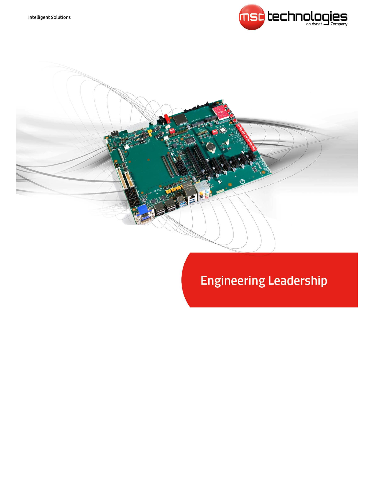
User Manual
COM ExpressTM Type 6 Carrier
MSC C6-MB-EVA
Evaluation Board
Hardware Rev. 4
Rev. 0.10 2015-02-05
Page 2

MSC C6-MB-EVA - PRELIMINARY - User Manual
2 / 63
Preface
Copyright Notice
Copyright © 2014 MSC Technologies GmbH. All rights reserved.
Copying of this document, and giving it to others and the use or communication of the
contents thereof, is forbidden without express authority. Offenders are liable to the payment
of damages.
All rights are reserved in the event of the grant of a patent or the registration of a utility model
or design.
Important Information
This documentation is intended for qualified audience only. The product described herein is
not an end user product. It was developed and manufactured for further processing by
trained personnel.
Disclaimer
Although this document has been generated with the utmost care no warranty or liability for
correctness or suitability for any particular purpose is implied. The information in this
document is provided “as is” and is subject to change without notice.
EMC Rules
This unit has to be installed in a shielded housing. If not installed in a properly shielded
enclosure, and used in accordance with the instruction manual, this product may cause radio
interference in which case the user may be required to take adequate measures at his or her
owns expense.
Trademarks
All used product names, logos or trademarks are property of their respective owners.
Certification
MSC Technologies GmbH is certified according to DIN EN ISO 9001:2000 standards.
Life-Cycle-Management
MSC products are developed and manufactured according to high quality standards. Our lifecycle-management assures long term availability through permanent product maintenance.
Technically necessary changes and improvements are introduced if applicable. A productchange-notification and end-of-life management process assures early information of our
customers.
Product Support
MSC engineers and technicians are committed to provide support to our customers
whenever needed.
Before contacting Technical Support of MSC Technologies GmbH, please consult the
respective pages on our web site at www.msc-technologies.eu for the latest documentation,
drivers and software downloads.
If the information provided there does not solve your problem, please contact our Technical
Support:
Email: [email protected]
Phone: +49 8165 906-200
Page 3

MSC C6-MB-EVA - PRELIMINARY - User Manual
3 / 63
Content
1 General Information ..................................................................................................... 6
1.1 Revision History........................................................................................................ 6
1.2 Reference Documents .............................................................................................. 6
1.3 Introduction ............................................................................................................... 7
2 Technical Description................................................................................................... 7
2.1 Key Features ............................................................................................................ 7
2.2 Block diagram ........................................................................................................... 9
2.3 Positioning of the Connectors, Jumpers and Switches............................................ 10
3 Mechanics ................................................................................................................. 12
3.1 Dimensions ............................................................................................................. 12
3.2 Assembly notes ...................................................................................................... 12
4 Hardware ................................................................................................................... 13
4.1 Plug-in Position of the COM Express module ......................................................... 13
4.2 PCI Express Lanes ................................................................ ................................ . 18
4.3 PCI Express x4 Slots .............................................................................................. 19
4.4 PCI Express x1 Slots .............................................................................................. 21
4.5 PCI Express Mini Card ........................................................................................... 22
4.6 PCI Express x16 Graphics Slot ............................................................................... 23
4.7 ADD2 Card Slot ...................................................................................................... 26
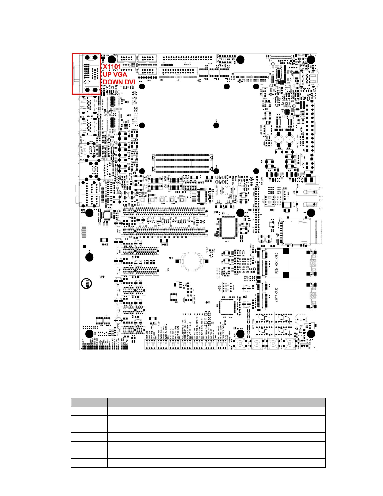
4.8 VGA Interface ......................................................................................................... 29
4.9 DVI-D Interface ....................................................................................................... 30
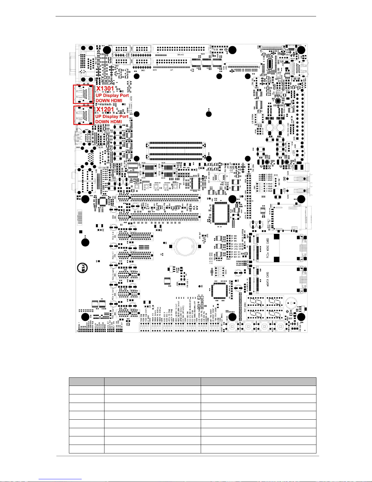
4.10 High Definition Multimedia Interface (HDMI) ........................................................ 31
4.11 Display Port (DP) ................................................................................................. 32
4.12 Embedded Display Port (eDP) ............................................................................. 33
4.13 Alternative Embedded Display Port and HDMI Connector ................................... 35
4.14 LVDS-Interface .................................................................................................... 36
4.14.1 LVDS EEPROM Socket ................................................................................ 37
4.14.2 Backlight Inverter Interface ........................................................................... 38
4.15 Audio ................................................................................................................... 39
4.15.1 HDA Connector ............................................................................................. 40
4.15.2 SPDIF ........................................................................................................... 40
4.15.3 HDA Codec Adapter (not available from Rev.4) ........................................... 40
4.16 SATA-Interface .................................................................................................... 41
4.17 mSATA Interface ................................................................................................. 42
4.18 USB Topology ..................................................................................................... 43
4.18.1 USB Power Supply ....................................................................................... 44
4.18.2 USB Connectors ........................................................................................... 44
4.18.3 USB Client Connector ................................................................................... 45
4.19 Ethernet............................................................................................................... 45
4.20 LPC Connector .................................................................................................... 45
4.21 GPIO ................................................................................................................... 47
4.21.1 GPIO Connector ........................................................................................... 48
4.21.2 SD Memory Card Connector ......................................................................... 48
4.22 COM Ports COM3 COM4 .................................................................................... 48
4.23 Super IO .............................................................................................................. 49
4.23.1 SIO Configuration ......................................................................................... 50
4.23.2 Parallel Port .................................................................................................. 50
4.23.3 COM Ports COM1 COM2 .............................................................................. 50
4.23.4 IrDA .............................................................................................................. 51
4.23.5 PS/2 Connector ............................................................................................ 51
4.23.6 Super IO Fan interface .................................................................................. 52
4.23.7 Super IO Hardware Monitor .......................................................................... 52
4.24 Fan Interface ....................................................................................................... 52
4.24.1 Intel Fan interface ......................................................................................... 52
4.25 Serial SMB EEPROM .......................................................................................... 53
Page 4

MSC C6-MB-EVA - PRELIMINARY - User Manual
4 / 63
4.26 Serial I2C-Bus EEPROM ................................ ................................ ..................... 54
4.26.1 Feature I2C EEPROM................................................................................... 54
4.26.2 User I2C EEPROM ....................................................................................... 54
4.27 External SPI BIOS-Flash ..................................................................................... 54
4.28 POST-Code Display ............................................................................................ 54
4.28.1 Lattice Programming Interface ...................................................................... 54
4.29 Feature Connector .............................................................................................. 56
4.30 Power Supply ATX Connector ............................................................................. 56
4.31 Power Supply Labor Connector ........................................................................... 57
4.32 Battery ................................................................................................................. 58
4.33 Beeper ................................................................................................................ 58
4.34 Power Button ....................................................................................................... 58
4.35 Reset Button ....................................................................................................... 58
4.36 Sleep Button ........................................................................................................ 58
4.37 Clear Event Button .............................................................................................. 58
4.38 LEDs ................................................................................................................... 59
4.39 WLAN LEDs ........................................................................................................ 59
4.40 DIP Switches ....................................................................................................... 60
4.41 Miscellaneous...................................................................................................... 60
4.41.1 Resistors for current measuring .................................................................... 60
4.41.2 Ground Pins ................................................................ ................................ .. 60
4.41.3 Power supply current measuring ................................................................... 61
4.42 Graphic Port Selection ......................................................................................... 62
4.42.1 JILI30 / eDP Selection................................................................................... 63
4.42.2 DDI Port Selection ........................................................................................ 63
Illustrations
Illustration 1 Block Diagram ................................................................................................... 9
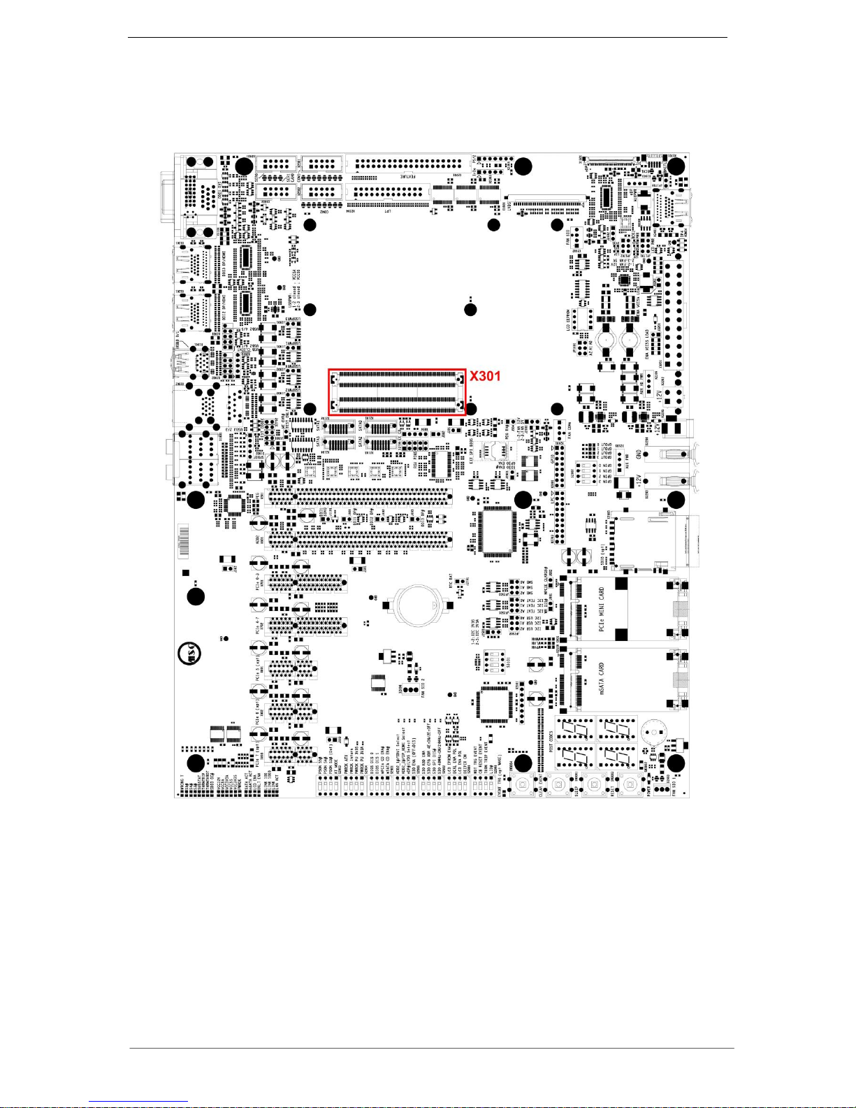
Illustration 2 Connectors overview ....................................................................................... 10
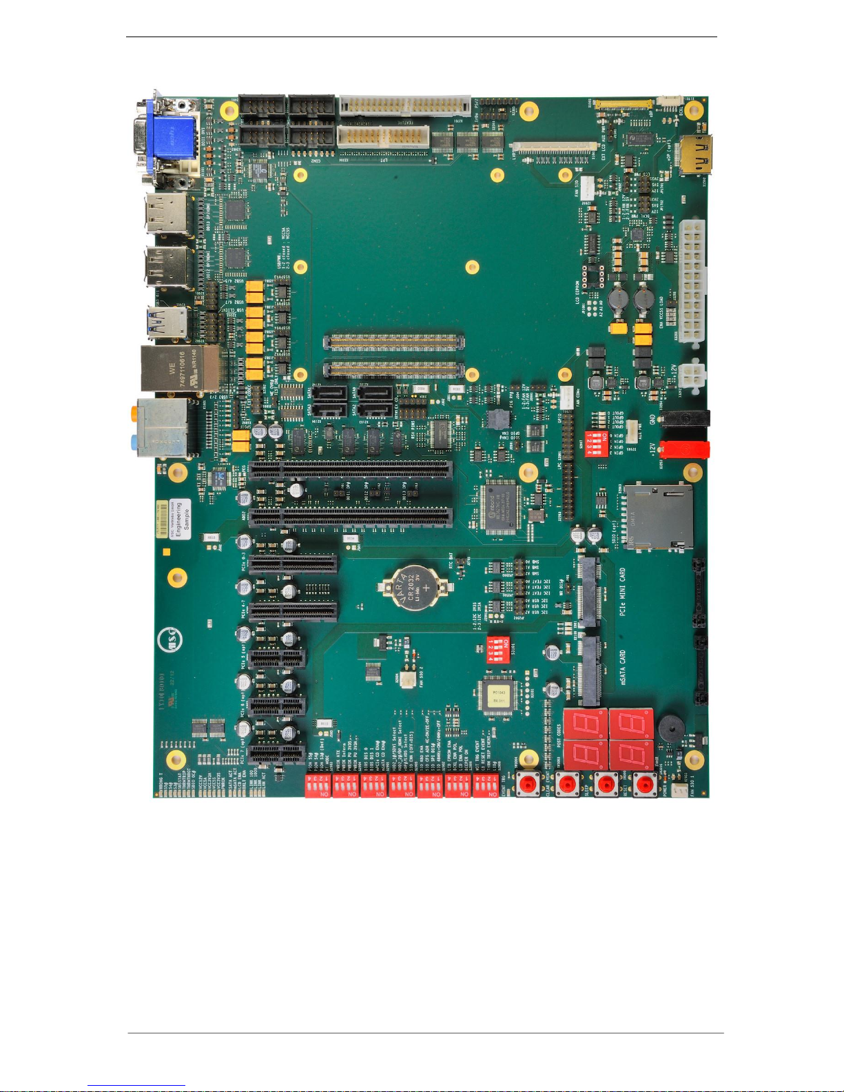
Illustration 3 Picture ............................................................................................................. 11
Illustration 4 Miscellaneous Parts ........................................................................................ 57
Illustration 5 Current Measurement...................................................................................... 61
Illustration 6 Block Diagram Graphics Ports ......................................................................... 62
Tables
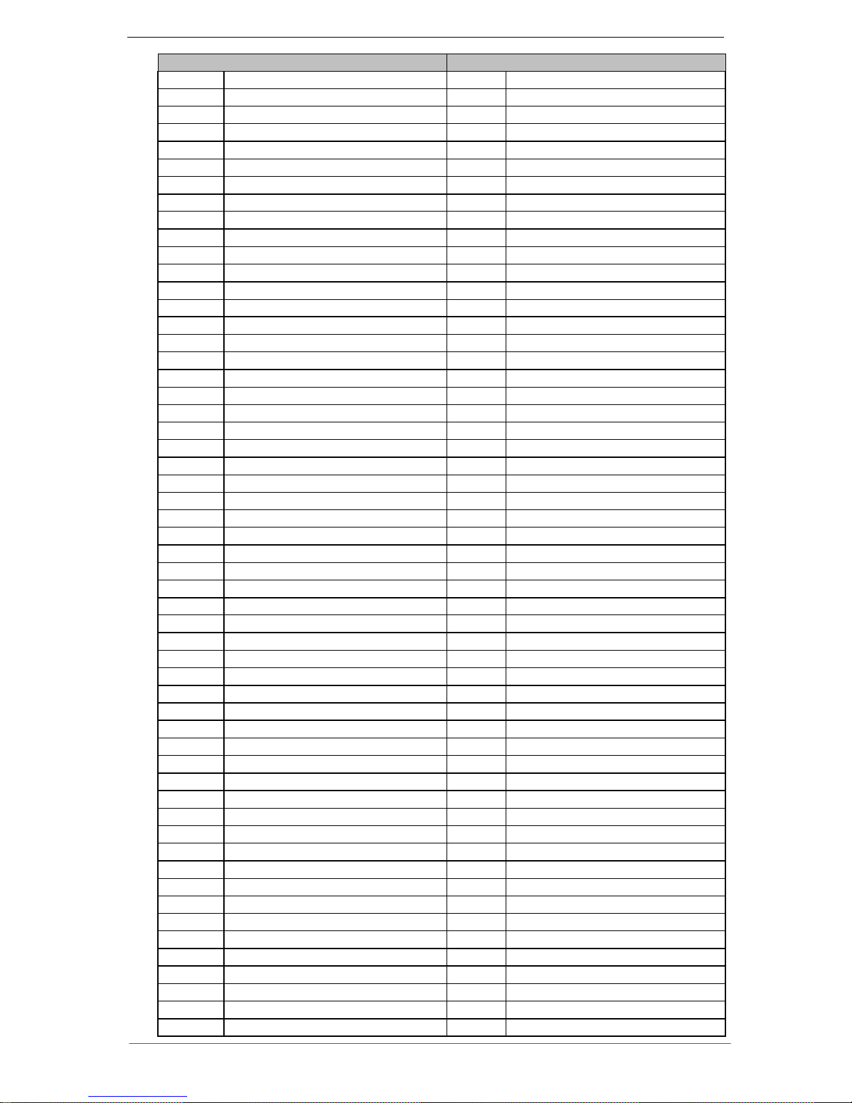
Table 1 COMExpress Connector Rows A and B ................................................................ 15
Table 2 COMExpress Connector Rows C and D ............................................................... 17
Table 3 Assignment PCIe Lane to connector reference ..................................................... 18
Table 4 PCIe Lane configuration ....................................................................................... 18
Table 5 Pin out PCI Express .............................................................................................. 20
Table 6 Pin out PCI Express .............................................................................................. 22
Table 7 Pin out PCI Express x16 Graphics Slot ................................................................. 25
Table 8 Pin out ADD2 Card Slot ................................ ........................................................ 28
Table 8 Pin-out VGA Interface ........................................................................................... 30
Table 9 Pin-out DVI-D Interface ......................................................................................... 30
Table 11 Pin-out HDMI ...................................................................................................... 32
Table 12 Pin-out Display Port ............................................................................................ 32
Table 13 Pin-out embedded Display Port .......................................................................... 34
Table 14 Pin-out eDP Backlight Power Supply Connector ................................................. 34
Table 15 Pin-out JILI30 LVDS-Interface ............................................................................ 37
Table 16 Pin-out LVDS EEPROM Socket .......................................................................... 38
Table 17 EEPROM Address JP1601 ................................................................................. 38
Table 18 Pin-out Backlight ................................................................................................. 38
Table 19 Pin-out LineOut ................................................................................................... 40
Page 5

MSC C6-MB-EVA - PRELIMINARY - User Manual
5 / 63
Table 20 Pin-out SPDIF ..................................................................................................... 40
Table 21 Pin-out HAD Codec Adapter ............................................................................... 40
Table 22 Assignment SATA Channel to Connector Reference .......................................... 41
Table 23 Pin-out mSATA socket ........................................................................................ 42
Table 24 Assignment USB Ports ....................................................................................... 43
Table 25 Pin-out USB 2.0 pin header ................................................................................ 44
Table 26 Pin-out USB 2.0 pin header ................................................................................ 44
Table 27 USB Client Connector ......................................................................................... 45
Table 28 Pin-out LPC-Slot ................................................................................................. 46
Table 29 Pin-out GPIO connector ...................................................................................... 48
Table 30 Pin-out COM Ports .............................................................................................. 48
Table 31 SIO Configuration ............................................................................................... 50
Table 32 Pin-out LPT Port ................................................................................................. 50
Table 33 Pin-out COM Ports .............................................................................................. 51
Table 34 Pin-out IrDA ........................................................................................................ 51
Table 35 Pin-out PS/2 Connector ...................................................................................... 51
Table 36 Pin-out SIO Fan Interface ................................................................................... 52
Table 37 Pin-out Fan Interface .......................................................................................... 52
Table 38 Jumper SMB EEPROM Address ......................................................................... 53
Table 39 Jumper Feature I2C EEPROM Address .............................................................. 54
Table 40 Jumper User I2C EEPROM Address .................................................................. 54
Table 41 Jumper BIOS selection ....................................................................................... 54
Table 42 POST-Code Selection......................................................................................... 54
Table 43 Pin-out Lattice Programming Interface ................................................................ 55
Table 44 Pin-out Feature connector .................................................................................. 56
Table 45 Pin-out Power IN3 connector .............................................................................. 57
Table 46 LEDs Overview ................................................................................................... 59
Table 47 DIP Switch Overview .......................................................................................... 60
Table 48 JILI30 / eDP Selection ........................................................................................ 63
Table 49 DDI Port Selection .............................................................................................. 63
Page 6
MSC C6-MB-EVA - PRELIMINARY - User Manual
6 / 63
1 General Information
1.1 Revision History
Rev.
Date
Description
0.1
26.07.2012
Initial Revision
0.2
10.8.2012
Minor changes
0.3
19.09.2012
Due to new board revision:
The eDP connector X1501 changed from 40 to 30 pin and the
pin assignment at COM ports has changed.
0.4
2012-11-08
Minor changes
0.5
2013-04-15
Adaption to new board revision (LY30E801)
0.6
2013-07-22
SD memory card slot, DIP-switch setting for LY30E801
0.7
2013-11-15
Remarks concerning to LY30E801 added
0.8
2014-03-19
Adaption to new board revision (LY40E801)
0.9
2014-09-05
New covering page
0.10
2015-02-05
Table44 Pin21 corrected
1.2 Reference Documents
[1] COM Express Module Base Specification
COM Express Revision 2.1
Last update: Apr10th, 2012
[2] PCI Local Bus Specification Rev. 2.1
PCI21.PDF
Last update: June 1st, 1995
http://www.pcisig.com
[3] JILI Specification
Jilim120.pdf
Last update: April 7th, 2003
http://www.jumptec.de/product/data/jili/index.html
[4] Serial ATA Specification
Serial ATA 1.0 gold.pdf
Last update: August 29th, 2002 Rev.1.0
http://www.sata-io.org/
[5] IEEE Std. 802.3-2002
802.3-2002.pdf
http://www.ieee.org
[6] Universal Bus Specification
usb_20.pdf
Last update: April 27th, 2000
http://www.usb.org
[7] Digital Video Interface DVI
dvi_10.pdf
Rev. 1.0 April 2nd, 1999
http://www.ddwg.org/
Page 7

MSC C6-MB-EVA - PRELIMINARY - User Manual
7 / 63
1.3 Introduction
COM Express™, is an open specification from the PICMG (PCI Industrial Computer
Manufacturer Group). It is a module concept to bring PCI Express and other new
technologies like SATA, USB 3.0 and different display interfaces onto a COM (Computer
On Module).
A COM Express™ module is plugged onto an application-specific base board which
provides the necessary I/O connectors and may also contain application-specific
additional logic circuitry.
Typically a COM Express module consists of CPU, chipset, memory, video controller,
Ethernet controller, BIOS Flash, SATA- and USB controller. More I/O controllers and all
I/O connectors are implemented on the base board on to which the COM Express
module can be plugged via one or two 220-pin SMD-connectors. Beside the power
supply also signals for PCIe bus, displays, SATA, USB, LPC etc. are present on these
connectors.
The type of interfaces that is led from the COM Express module to the base board
depends on the type of module that is used. The COM Express specification defines
seven different types which differ in number and pin assignment of the module
connectors.
Thanks to the standardized mechanics and interfaces the system can be scaled
arbitrarily. In spite of the modular concept the systems design is very flat and compact.
COM Express modules require a base-board for successful operation.
The base board described below acts as an evaluation board for COM Express modules
with pin-out Type 6.
2 Technical Description
2.1 Key Features
The MSC C6-MB-EVA COM Express base board is designed as a type 6 carrier board.
Key features include:
Interface for COM Express module type 6 up to basic form factor
Dual 220 pin connector (440 pins)
1 PCIe x4 slot
4 PCIe x1 slots shared with 1 PCIe x4 slot and / or PCIe mini card
PCIe x16 graphics slot (PEG)
VGA interface
LVDS interface (JILI30)
3 Digital Display Interfaces /shared with card slot
1 DVI connector
2 HDMI connectors / 2 DP connectors
1 eDP connector (40pin)
4 USB3.0 root hub interfaces
4 USB2.0 root hub interfaces
4 SATA channels up to 300MB/s
mSATA shared with one standard SATA channel
High definition digital audio codec ALC888 or pin header
6 audio jacks
SPDIF on pin header
GBit Ethernet interface
Feature connector
Page 8

MSC C6-MB-EVA - PRELIMINARY - User Manual
8 / 63
LPC header
Pin header for GPIOs
SuperIO W83627HG
PS/2, 2x COM (SIO), LPT, IRDA, fan interfaces
Power supply via ATX connector or +12V only
POST display on LPC
Serial EEPROM on I²C-Bus
Serial EEPROM on SMBus
On-board SPI Flash socket
Beeper
2x COM (module)
3V battery
Note: Support for all above features will also depend on the COM Express module being
used. Not all modules support the maximum number of interfaces.
Page 9
MSC C6-MB-EVA - PRELIMINARY - User Manual
9 / 63
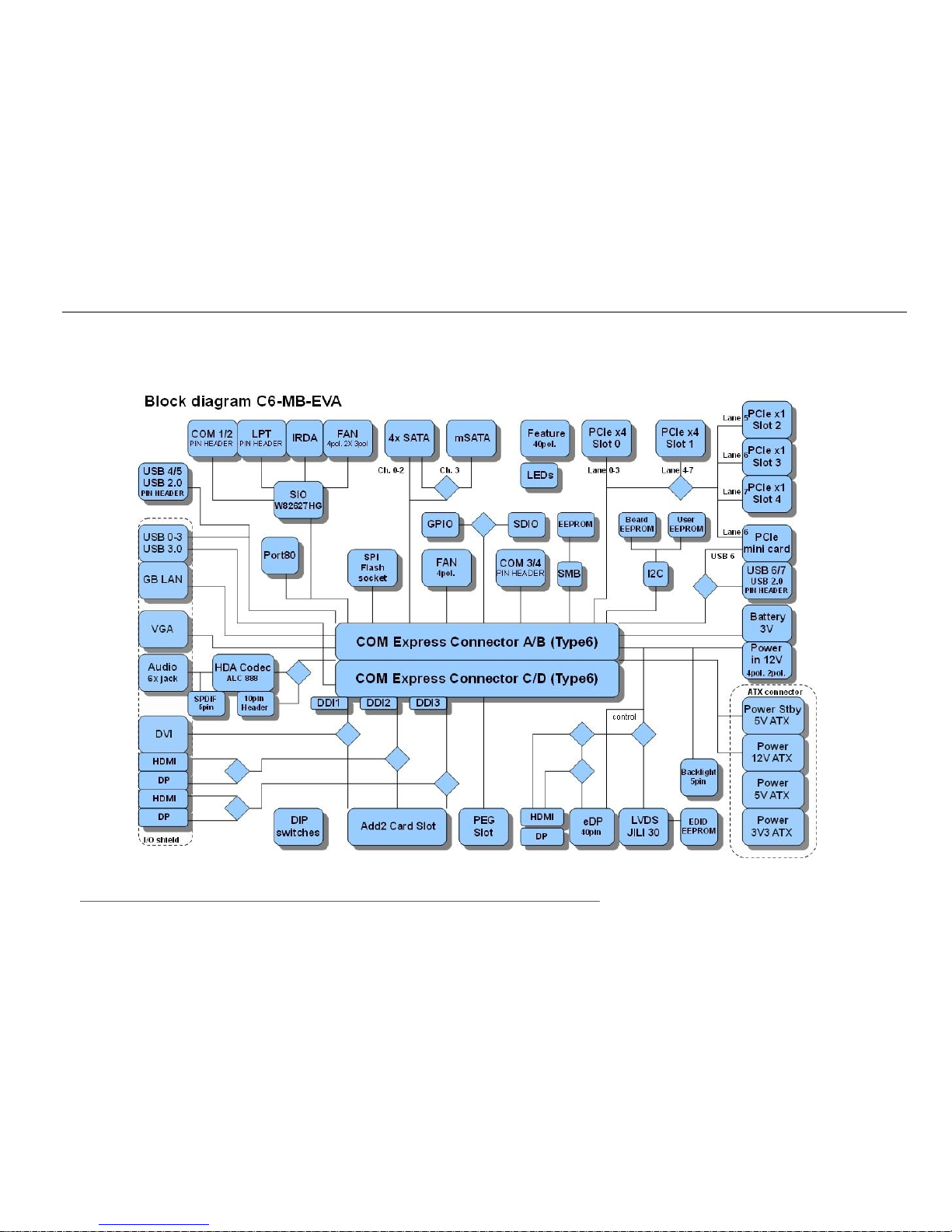
2.2 Block diagram
Illustration 1 Block Diagram
Page 10
MSC C6-MB-EVA - PRELIMINARY - User Manual
10 / 63
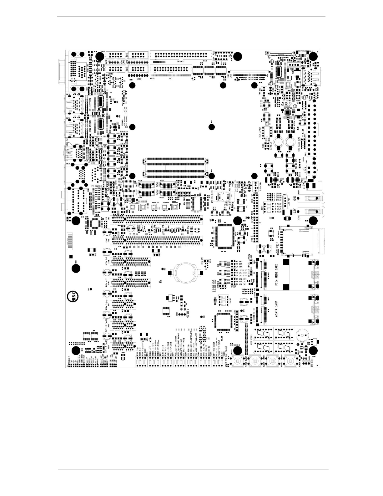
2.3 Positioning of the Connectors, Jumpers and Switches
Illustration 2 Connectors overview
Page 11
MSC C6-MB-EVA - PRELIMINARY - User Manual
11 / 63
Illustration 3 Picture
Page 12
MSC C6-MB-EVA - PRELIMINARY - User Manual
12 / 63
3 Mechanics
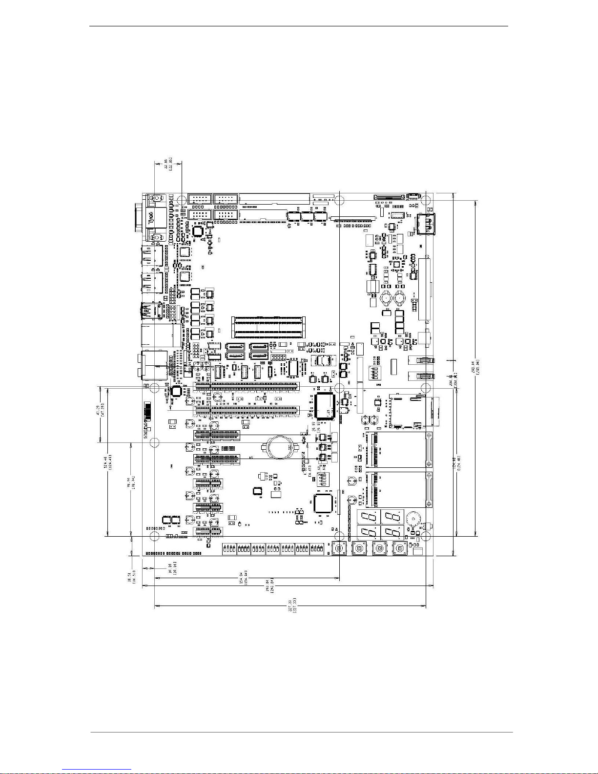
3.1 Dimensions
Dimension: 243.8 mm x 304.8 mm
Width: 1.6 mm + /-10%
Tolerances of the drill holes: +/- 0.1mm in X and Y
Tolerances of the diameter: + 0.1 mm
3.2 Assembly notes
Use these bolts for mounting different form factors:
COM Express Mini: 4x M2.5 x 5mm bolt
COM Express Compact: 4x M2.5 x 5mm bolt
COM Express Basic: 5x M2.5 x 5mm bolt
Page 13
MSC C6-MB-EVA - PRELIMINARY - User Manual
13 / 63
4 Hardware
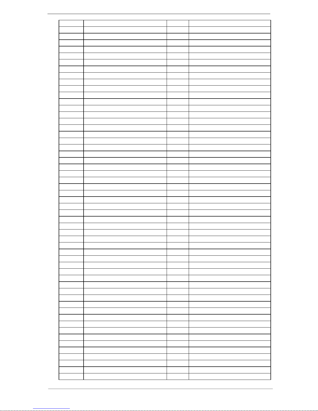
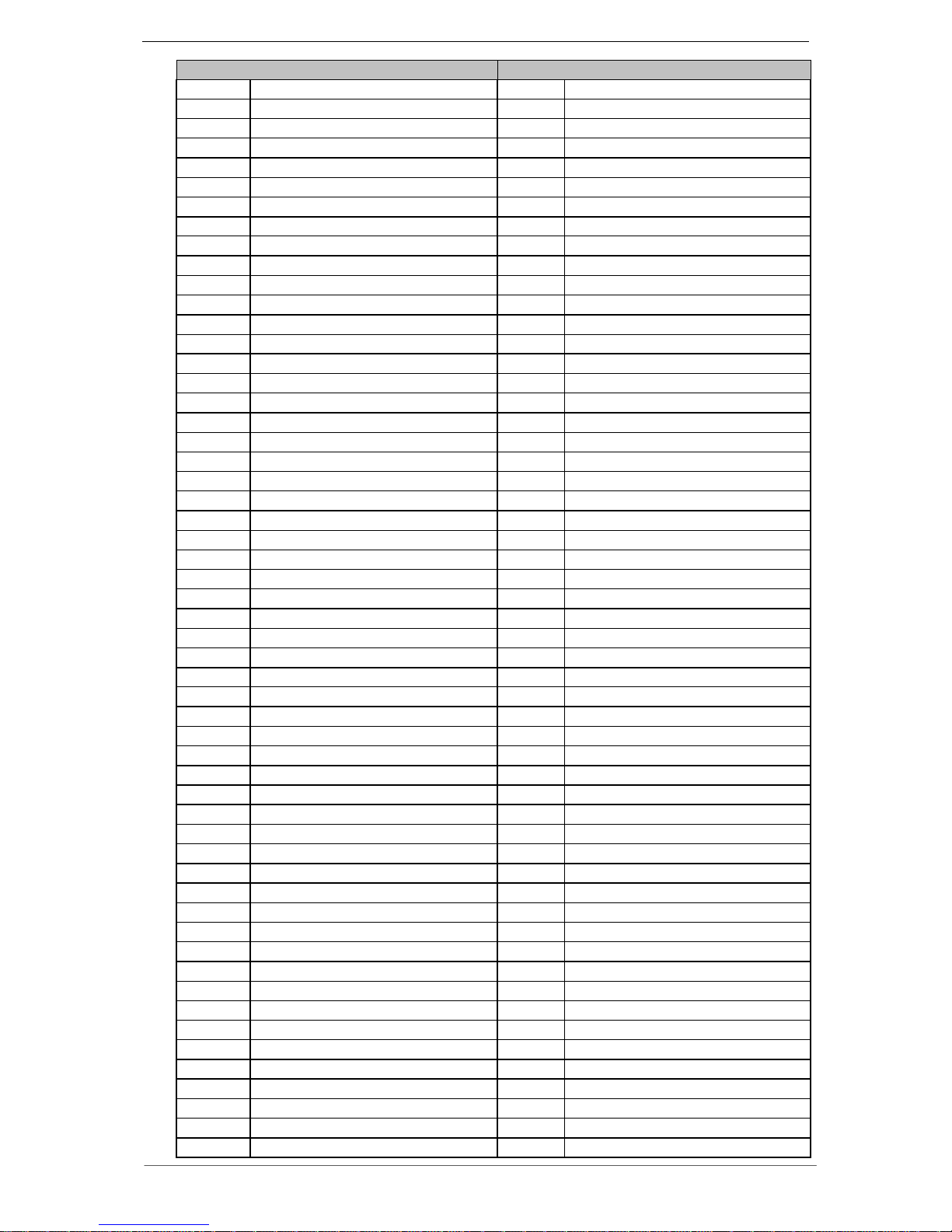
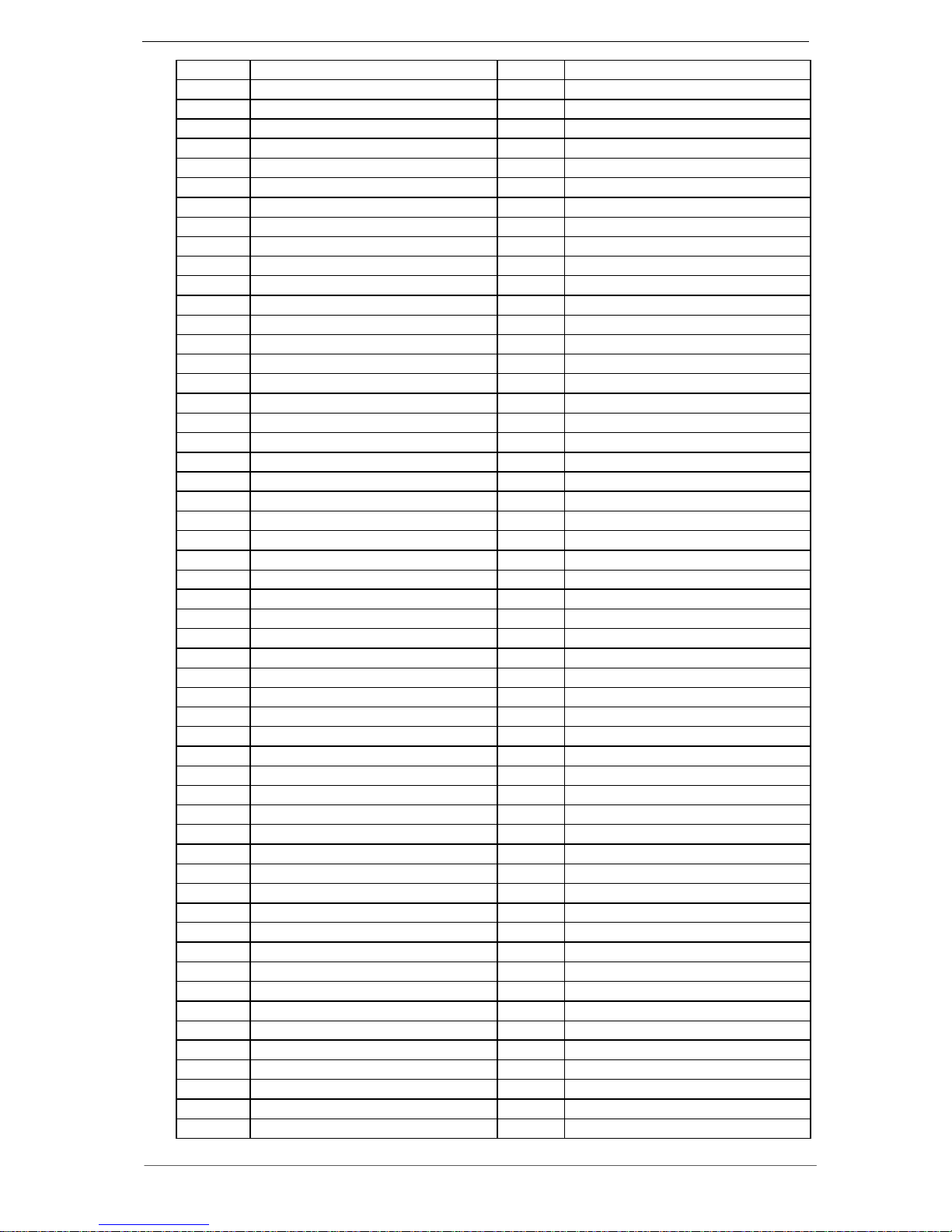
4.1 Plug-in Position of the COM Express module
Socket for a COM Express type 6 module is available on the base board.
Following form factors are supported:
Mini Module
Compact Module
Basic Module
Specification:
Reference: X301
Connector:AMP / Tyco 3-1827233-6
0.5 mm pitch free height 440 pin 5H plug (combination of two 220pin plugs)
Pin-out: Refer to COM Express specification for type 6 module
[1]
Page 14
MSC C6-MB-EVA - PRELIMINARY - User Manual
14 / 63
Row A
Row B
A1
GND
B1
GND
A2
GBE0_MDI3-
B2
GBE0_ACT#
A3
GBE0_MDI3+
B3
LPC_FRAME#
A4
GBE0_LINK100#
B4
LPC_AD0
A5
GBE0_LINK1000#
B5
LPC_AD1
A6
GBE0_MDI2-
B6
LPC_AD2
A7
GBE0_MDI2+
B7
LPC_AD3
A8
GBE0_LINK#
B8
LPC_DRQ0#
A9
GBE0_MDI1-
B9
LPC_DRQ1#
A10
GBE0_MDI1+
B10
LPC_CLK
A11
GND
B11
GND
A12
GBE0_MDI0-
B12
PWRBTN#
A13
GBE0_MDI0+
B13
SMB_CK
A14
GBE0_CTREF
B14
SMB_DAT
A15
SUS_S3#
B15
SMB_ALERT#
A16
SATA0_TX+
B16
SATA1_TX+
A17
SATA0_TX-
B17
SATA1_TX-
A18
SUS_S4#
B18
SUS_STAT#
A19
SATA0_RX+
B19
SATA1_RX+
A20
SATA0_RX-
B20
SATA1_RX-
A21
GND
B21
GND
A22
SATA2_TX+
B22
SATA3_TX+
A23
SATA2_TX-
B23
SATA3_TX-
A24
SUS_S5#
B24
PWR_OK
A25
SATA2_RX+
B25
SATA3_RX+
A26
SATA2_RX-
B26
SATA3_RX-
A27
BATLOW#
B27
WDT
A28
ATA_ACT#
B28
AC/HDA_SDIN2
A29
AC/HDA_SYNC
B29
AC/HDA_SDIN1
A30
AC/HDA_RST#
B30
AC/HDA_SDIN0
A31
GND
B31
GND
A32
AC/HDA_BITCLK
B32
SPKR
A33
AC/HDA_SDOUT
B33
I2C_CK
A34
BIOS_DIS0#
B34
I2C_DAT
A35
THRMTRIP#
B35
THRM#
A36
USB6-
B36
USB7-
A37
USB6+
B37
USB7+
A38
USB_6_7_OC#
B38
USB_4_5_OC#
A39
USB4-
B39
USB5-
A40
USB4+
B40
USB5+
A41
GND
B41
GND
A42
USB2-
B42
USB3-
A43
USB2+
B43
USB3+
A44
USB_2_3_OC#
B44
USB_0_1_OC#
A45
USB0-
B45
USB1-
A46
USB0+
B46
USB1+
A47
VCC_RTC
B47
EXCD1_PERST#
A48
EXCD0_PERST#
B48
EXCD1_CPPE#
A49
EXCD0_CPPE#
B49
SYS_RESET#
A50
LPC_SERIRQ
B50
CB_RESET#
A51
GND
B51
GND
A52
PCIE_TX5+
B52
PCIE_RX5+
A53
PCIE_TX5-
B53
PCIE_RX5-
A54
GPI0
B54
GPO1
A55
PCIE_TX4+
B55
PCIE_RX4+
Page 15
MSC C6-MB-EVA - PRELIMINARY - User Manual
15 / 63
A56
PCIE_TX4-
B56
PCIE_RX4-
A57
GND
B57
GPO2
A58
PCIE_TX3+
B58
PCIE_RX3+
A59
PCIE_TX3-
B59
PCIE_RX3-
A60
GND
B60
GND
A61
PCIE_TX2+
B61
PCIE_RX2+
A62
PCIE_TX2-
B62
PCIE_RX2-
A63
GPI1
B63
GPO3
A64
PCIE_TX1+
B64
PCIE_RX1+
A65
PCIE_TX1-
B65
PCIE_RX1-
A66
GND
B66
WAKE0#
A67
GPI2
B67
WAKE1#
A68
PCIE_TX0+
B68
PCIE_RX0+
A69
PCIE_TX0-
B69
PCIE_RX0-
A70
GND
B70
GND
A71
LVDS_A0+
B71
LVDS_B0+
A72
LVDS_A0-
B72
LVDS_B0-
A73
LVDS_A1+
B73
LVDS_B1+
A74
LVDS_A1-
B74
LVDS_B1-
A75
LVDS_A2+
B75
LVDS_B2+
A76
LVDS_A2-
B76
LVDS_B2-
A77
LVDS_VDD_EN
B77
LVDS_B3+
A78
LVDS_A3+
B78
LVDS_B3-
A79
LVDS_A3-
B79
LVDS_BKLT_EN
A80
GND
B80
GND
A81
LVDS_A_CK+
B81
LVDS_B_CK+
A82
LVDS_A_CK-
B82
LVDS_B_CK-
A83
LVDS_I2C_CK
B83
LVDS_BKLT_CTRL
A84
LVDS_I2C_DAT
B84
VCC_5V_SBY
A85
GPI3
B85
VCC_5V_SBY
A86
RSVD
B86
VCC_5V_SBY
A87
eDP_HPD
B87
VCC_5V_SBY
A88
PCIE0_CK_REF+
B88
BIOS_DIS1#
A89
PCIE0_CK_REF-
B89
VGA_RED
A90
GND
B90
GND
A91
SPI_POWER
B91
VGA_GRN
A92
SPI_MISO
B92
VGA_BLU
A93
GPO0
B93
VGA_HSYNC
A94
SPI_CLK
B94
VGA_VSYNC
A95
SPI_MOSI
B95
VGA_I2C_CK
A96
TPM_PP
B96
VGA_I2C_DAT
A97
TYPE10#
B97
SPI_CS#
A98
SER0_TX
B98
RSVD
A99
SER0_RX
B99
RSVD
A100
GND
B100
GND
A101
SER1_TX
B101
FAN_PWNOUT
A102
SER1_RX
B102
FAN_TACHIN
A103
LID#
B103
SLEEP#
A104
VCC_12V
B104
VCC_12V
A105
VCC_12V
B105
VCC_12V
A106
VCC_12V
B106
VCC_12V
A107
VCC_12V
B107
VCC_12V
A108
VCC_12V
B108
VCC_12V
A109
VCC_12V
B109
VCC_12V
A110
GND
B110
GND
Table 1 COMExpress Connector Rows A and B
Page 16
MSC C6-MB-EVA - PRELIMINARY - User Manual
16 / 63
Row C
Row D
C1
GND
D1
GND
C2
GND
D2
GND
C3
USB_SSRX0-
D3
USB_SSTX0-
C4
USB_SSRX0+
D4
USB_SSTX0+
C5
GND
D5
GND
C6
USB_SSRX1-
D6
USB_SSTX1-
C7
USB_SSRX1+
D7
USB_SSTX1+
C8
GND
D8
GND
C9
USB_SSRX2-
D9
USB_SSTX2-
C10
USB_SSRX2+
D10
USB_SSTX2+
C11
GND
D11
GND
C12
USB_SSRX3-
D12
USB_SSTX3-
C13
USB_SSRX3+
D13
USB_SSTX3+
C14
GND
D14
GND
C15
DDI1_PAIR6+
D15
DDI1_CTRLCLK_AUX+
C16
DDI1_PAIR6-
D16
DDI1_CTRLDATA_AUX-
C17
RSVD
D17
RSVD
C18
RSVD
D18
RSVD
C19
PCIE_RX6+
D19
PCIE_TX6+
C20
PCIE_RX6-
D20
PCIE_TX6-
C21
GND
D21
GND
C22
PCIE_RX7+
D22
PCIE_TX7+
C23
PCIE_RX7-
D23
PCIE_TX7-
C24
DDI1_HPD
D24
RSVD
C25
DDI1_PAIR4+
D25
RSVD
C26
DDI1_PAIR4-
D26
DDI1_PAIR0+
C27
RSVD
D27
DDI1_PAIR0-
C28
RSVD
D28
RSVD
C29
DDI1_PAIR5+
D29
DDI1_PAIR1+
C30
DDI1_PAIR5-
D30
DDI1_PAIR1-
C31
GND
D31
GND
C32
DDI2_CTRLCLK_AUX+
D32
DDI1_PAIR2+
C33
DDI2_CTRLDATA_AUX-
D33
DDI1_PAIR2-
C34
DDI2_DDC_AUX_SEL
D34
DDI1_DDC_AUX_SEL
C35
RSVD
D35
RSVD
C36
DDI3_CTRLCLK_AUX+
D36
DDI1_PAIR3+
C37
DDI3_CTRLDATA_AUX-
D37
DDI1_PAIR3-
C38
DDI3_DDC_AUX_SEL
D38
RSVD
C39
DDI3_PAIR0+
D39
DDI2_PAIR0+
C40
DDI3_PAIR0-
D40
DDI2_PAIR0-
C41
GND
D41
GND
C42
DDI3_PAIR1+
D42
DDI3_PAIR1+
C43
DDI3_PAIR1-
D43
DDI3_PAIR1-
C44
DDI3_HPD
D44
DDI2_HPD
C45
RSVD
D45
RSVD
C46
DDI3_PAIR2+
D46
DDI3_PAIR2+
C47
DDI3_PAIR2-
D47
DDI3_PAIR2-
C48
RSVD
D48
RSVD
C49
DDI3_PAIR3+
D49
DDI3_PAIR3+
C50
DDI3_PAIR3-
D50
DDI3_PAIR3-
C51
GND
D51
GND
C52
PEG_RX0+
D52
PEG_TX0+
C53
PEG_RX0-
D53
PEG_TX0-
C54
TYPE0#
D54
PEG_LANE_RV#
C55
PEG_RX1+
D55
PEG_TX1+
Page 17
MSC C6-MB-EVA - PRELIMINARY - User Manual
17 / 63
C56
PEG_RX1-
D56
PEG_TX1-
C57
TYPE1#
D57
TYPE2#
C58
PEG_RX2+
D58
PEG_TX2+
C59
PEG_RX2-
D59
PEG_TX2-
C60
GND
D60
GND
C61
PEG_RX3+
D61
PEG_TX3+
C62
PEG_RX3-
D62
PEG_TX3-
C63
RSVD
D63
RSVD
C64
RSVD
D64
RSVD
C65
PEG_RX4+
D65
PEG_TX4+
C66
PEG_RX4-
D66
PEG_TX4-
C67
RSVD
D67
GND
C68
PEG_RX5+
D68
PEG_TX5+
C69
PEG_RX5-
D69
PEG_TX5-
C70
GND
D70
GND
C71
PEG_RX6+
D71
PEG_TX6+
C72
PEG_RX6-
D72
PEG_TX6-
C73
GND
D73
GND
C74
PEG_RX7+
D74
PEG_TX7+
C75
PEG_RX7-
D75
PEG_TX7-
C76
GND
D76
GND
C77
RSVD
D77
RSVD
C78
PEG_RX8+
D78
PEG_TX8+
C79
PEG_RX8-
D79
PEG_TX8-
C80
GND
D80
GND
C81
PEG_RX9+
D81
PEG_TX9+
C82
PEG_RX9-
D82
PEG_TX9-
C83
RSVD
D83
RSVD
C84
GND
D84
GND
C85
PEG_RX10+
D85
PEG_TX10+
C86
PEG_RX10-
D86
PEG_TX10-
C87
GND
D87
GND
C88
PEG_RX11+
D88
PEG_TX11+
C89
PEG_RX11-
D89
PEG_TX11-
C90
GND
D90
GND
C91
PEG_RX12+
D91
PEG_TX12+
C92
PEG_RX12-
D92
PEG_TX12-
C93
GND
D93
GND
C94
PEG_RX13+
D94
PEG_TX13+
C95
PEG_RX13-
D95
PEG_TX13-
C96
GND
D96
GND
C97
RSVD
D97
PEG_ENABLE#
C98
PEG_RX14+
D98
PEG_TX14+
C99
PEG_RX14-
D99
PEG_TX14-
C100
GND
D100
GND
C101
PEG_RX15+
D101
PEG_TX15+
C102
PEG_RX15-
D102
PEG_TX15-
C103
GND
D103
GND
C104
VCC_12V
D104
VCC_12V
C105
VCC_12V
D105
VCC_12V
C106
VCC_12V
D106
VCC_12V
C107
VCC_12V
D107
VCC_12V
C108
VCC_12V
D108
VCC_12V
C109
VCC_12V
D109
VCC_12V
C110
GND
D110
GND
Table 2 COMExpress Connector Rows C and D
Page 18
MSC C6-MB-EVA - PRELIMINARY - User Manual
18 / 63
4.2 PCI Express Lanes
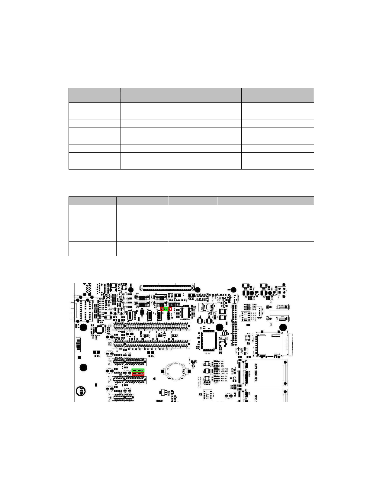
8 PCIe lanes are defined at the COM Express module.
Some lanes can be routed to various connectors.
Note: The number of PCIe lanes available will depend on the COM Express module used – not all
modules can support 8 PCIe lanes.
PCIe Lane
References
default
References
Change via resistors
References
Change via switch
PCIe Lane 0
X701 Slot 0
PCIe Lane 1
X701 Slot 0
PCIe Lane 2
X701 Slot 0
PCIe Lane 3
X701 Slot 0
PCIe Lane 4
X702 Slot 1
PCIe Lane 5
X801 Slot 2
X702 Slot 1
PCIe Lane 6
X802 Slot 3
X702 Slot 1
X901 Mini PCIe
PCIe Lane 7
X803 Slot 4
X702 Slot 1
Table 3 Assignment PCIe Lane to connector reference
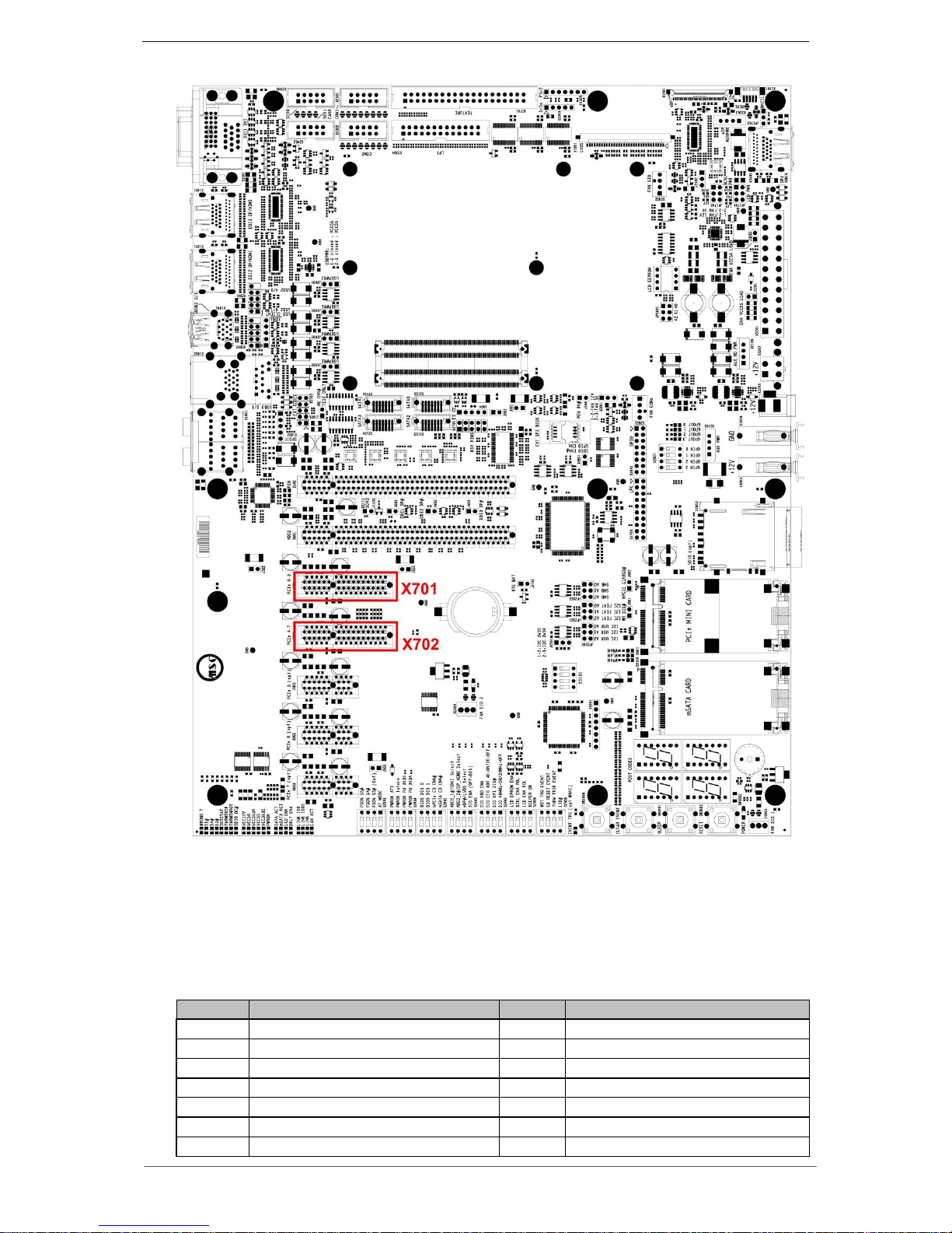
To change PCIe lanes from Slot 1 to Slots 2/3/4 remove resistors and replace them at:
PCIe Lane
Remove (red)
place at (green)
Mini PCIe
PCIe Lane 5
RJ713, RJ714,
RJ715, RJ716
RJ701, RJ702,
RJ707, RJ708
PCIe Lane 6
RJ717, RJ718,
RJ719, RJ720
RJ703, RJ704,
RJ709, RJ710
Don’t move resistors. When
plugging the device, lane 6
switches automatic.
PCIe Lane 7
RJ721, RJ722,
RJ723, RJ724
RJ705, RJ706,
RJ711, RJ712
Table 4 PCIe Lane configuration
Page 19
MSC C6-MB-EVA - PRELIMINARY - User Manual
19 / 63
4.3 PCI Express x4 Slots
Specification:
References: X701, X702
Connector:FCI 10018784
Pin-out: Refer to PCI express specification
PCIe slots are not hot-plug capable
Pin
Signal
Pin
Signal
A1
PRSNT1#
B1
12V
A2
12V
B2
12V
A3
12V
B3
12V
A4
GND
B4
GND
A5
JTAG_TCK
B5
SMB_CLK
A6
JTAG_TDI
B6
SMB_DAT
A7
JTAG_TDO
B7
GND
Page 20
MSC C6-MB-EVA - PRELIMINARY - User Manual
20 / 63
A8
JTAG_TMS
B8
3V3
A9
3V3
B9
JTAG_RST#
A10
3V3
B10
3V3_AUX
A11
PE_RST#
B11
WAKE#
KEY
A12
GND
B12
RSVD
A13
REFCLK+
B13
GND
A14
REFCLK-
B14
PET_p0
A15
GND
B15
PET_n0
A16
PER_p0
B16
GND
A17
PER_n0
B17
PRSNT2#
A18
GND
B18
GND
A19
RSVD
B19
PET_p1
A20
GND
B20
PET_n1
A21
PER_p1
B21
GND
A22
PER_n1
B22
PRSNT2#
A23
GND
B23
PET_p2
A24
GND
B24
PET_n2
A25
PER_p2
B25
GND
A26
PER_n2
B26
GND
A27
GND
B27
PET_p3
A28
GND
B28
PET_n3
A29
PER_p3
B29
GND
A30
PER_n3
B30
RSVD
A31
GND
B31
PRSNT2#
A32
RSVD
B32
GND
Table 5 Pin out PCI Express
Page 21
MSC C6-MB-EVA - PRELIMINARY - User Manual
21 / 63
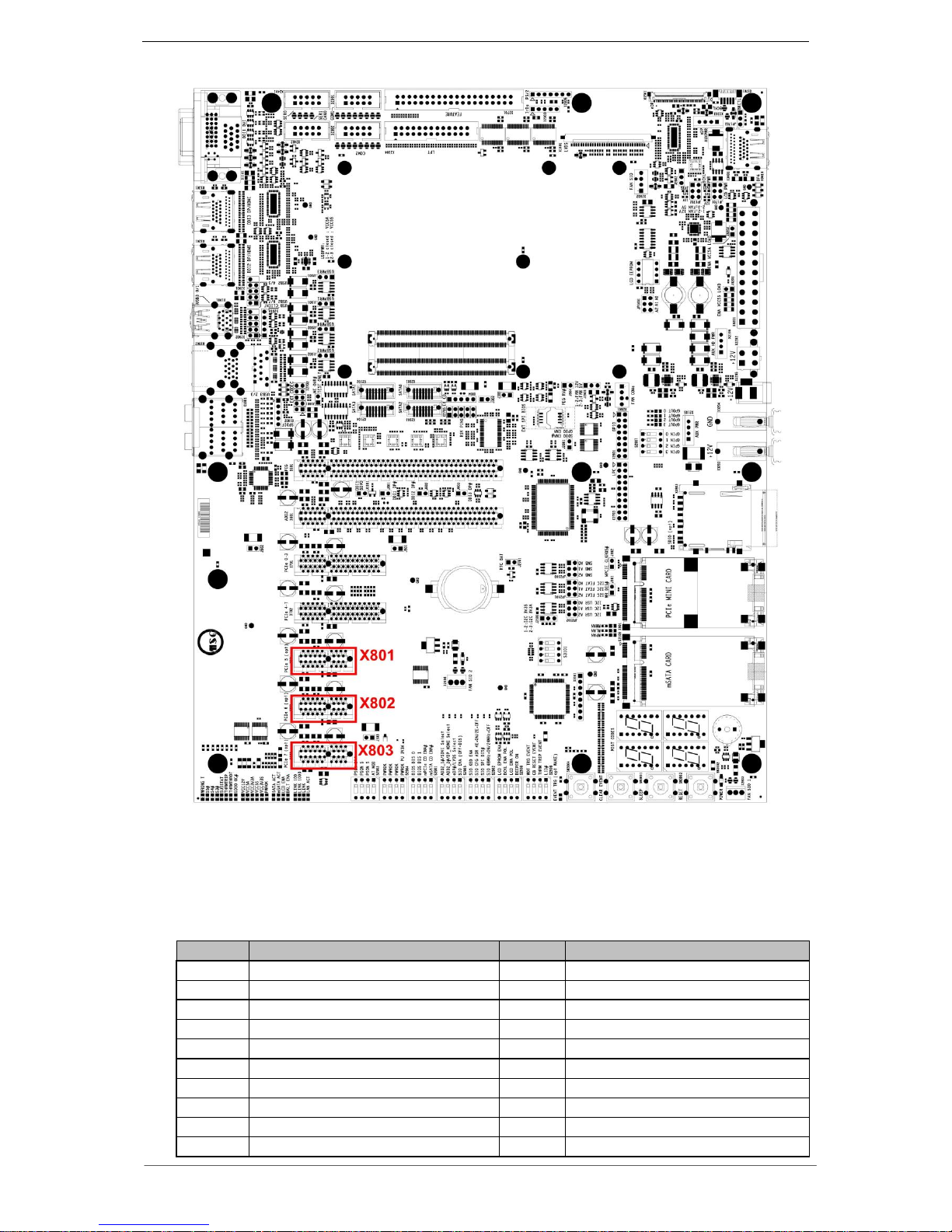
4.4 PCI Express x1 Slots
Specification:
References: X801 – X803
Connector:AMP / Tyco 4-1612163-1
Pin-out: Refer to PCI express specification
PCIe slots are not hot-plug capable
Pin
Signal
Pin
Signal
A1
PRSNT1#
B1
12V
A2
12V
B2
12V
A3
12V
B3
12V
A4
GND
B4
GND
A5
JTAG_TCK
B5
SMB_CLK
A6
JTAG_TDI
B6
SMB_DAT
A7
JTAG_TDO
B7
GND
A8
JTAG_TMS
B8
3V3
A9
3V3
B9
JTAG_RST#
A10
3V3
B10
3V3_AUX
Page 22
MSC C6-MB-EVA - PRELIMINARY - User Manual
22 / 63
A11
PE_RST#
B11
WAKE#
KEY
A12
GND
B12
RSVD
A13
REFCLK+
B13
GND
A14
REFCLK-
B14
PET_p0
A15
GND
B15
PET_n0
A16
PER_p0
B16
GND
A17
PER_n0
B17
PRSNT2#
A18
GND
B18
GND
Table 6 Pin out PCI Express
4.5 PCI Express Mini Card
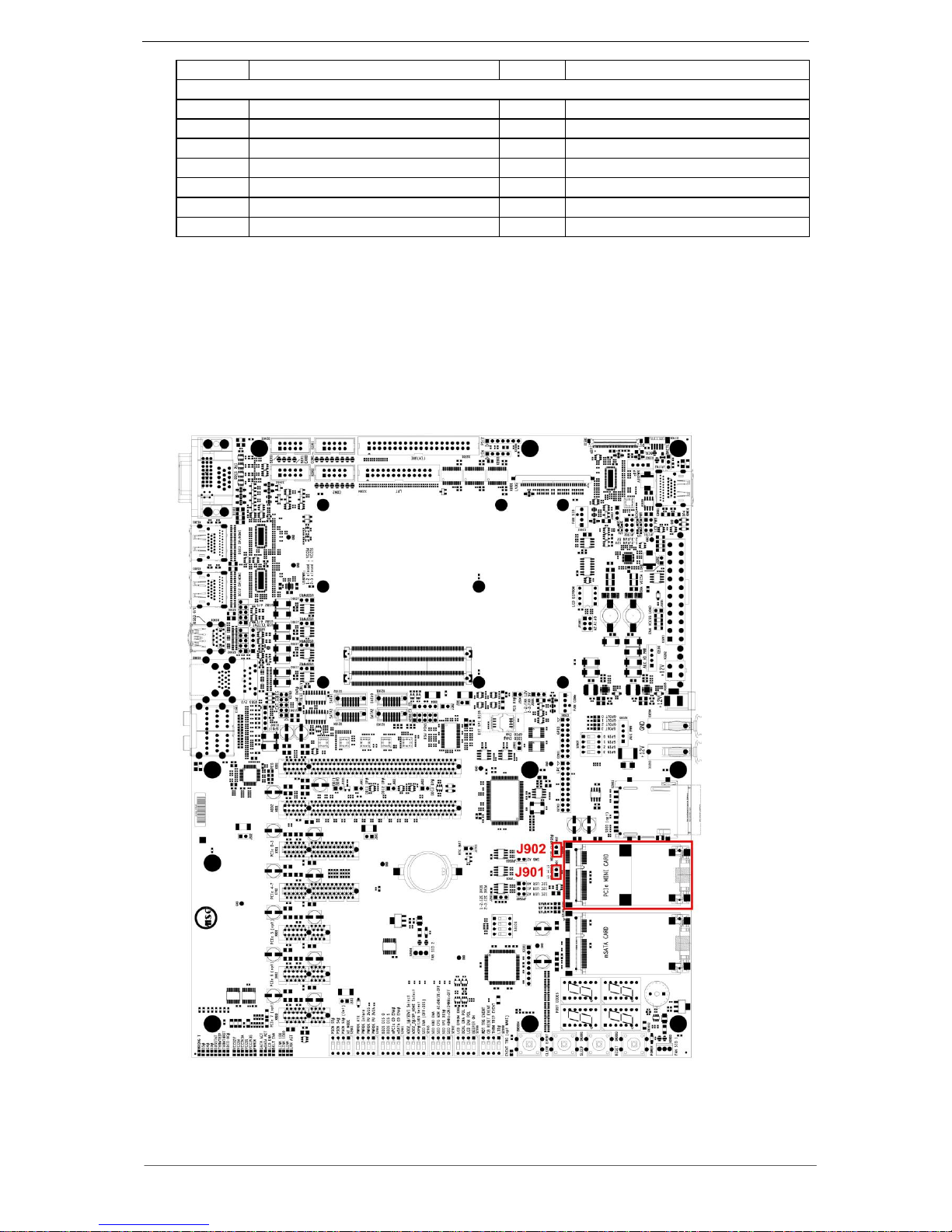
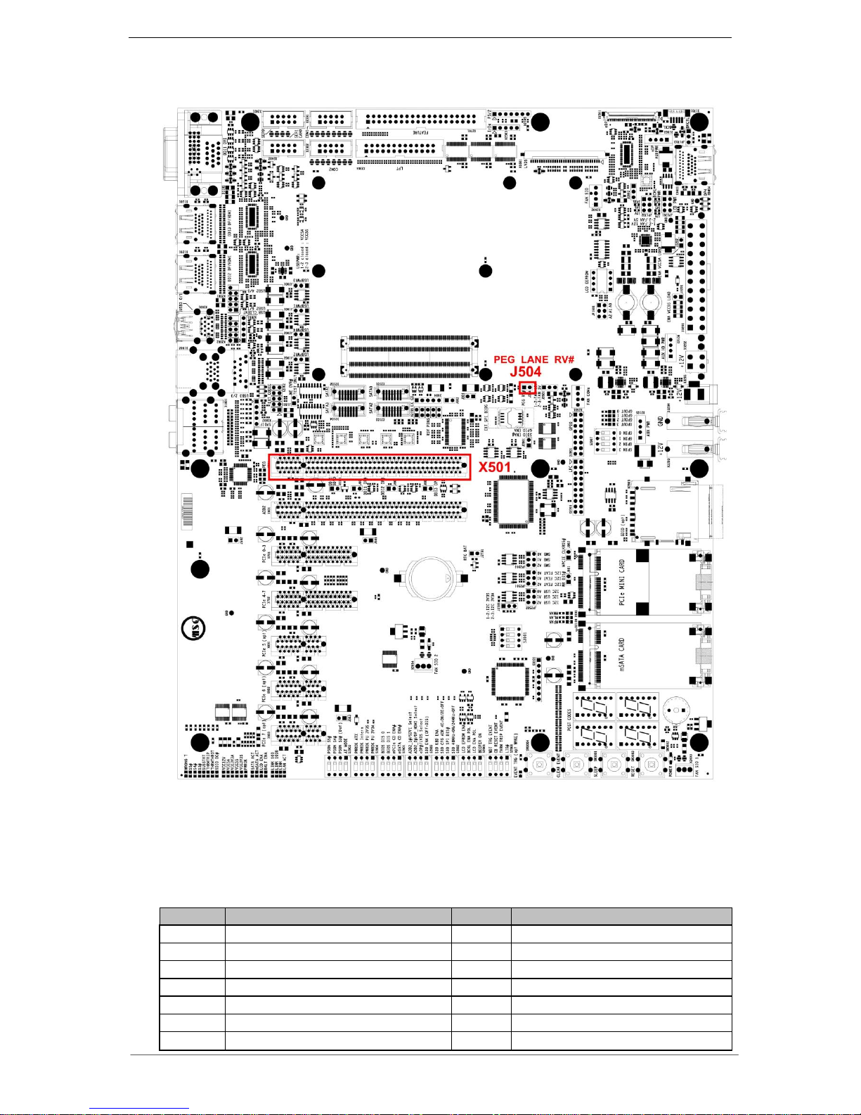
PCIe Lane 6 and the signals from USB port 6 switch automatic to this slot if a card is plugged. It
can be selected with DIP switch 2 at S2901. If the Mini Card slot is selected, PCIe-Slot 3 and
USB port 6 at X2002 are no longer useable. With the W_DISABLE# jumper J901 the card slot
can be set write protected. If the assembled Mini Card do not support CLKREQ# signal, the
jumper J902 enables the PCIe-clock signal at the Mini Card slot.
Note: At rev. 3 carrier (LY30E801) the USB port 6 signals are not routed to X901. They are still
useable at X2002.
Specification:
References: X901
Connector: Molex 67910-9000
Pin-out: Refer to PCIe Mini Card Specification
Page 23
MSC C6-MB-EVA - PRELIMINARY - User Manual
23 / 63
4.6 PCI Express x16 Graphics Slot
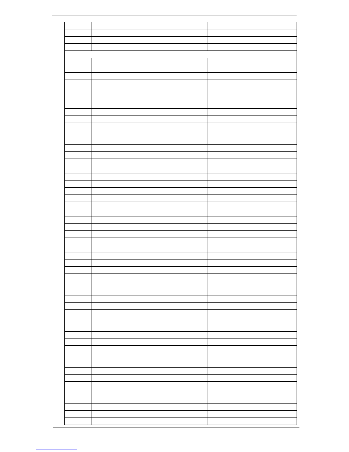
A PCIe x16 graphics slot is provided for insertion of PEG graphics cards.
Specification:
References: X501
Connector:AMP / Tyco 4-1612163-4
Pin-out: Refer to PCI express specification
Pin D54 can be set to ground with PEG_LANE_RV# jumper J504.
Pin
Signal
Pin
Signal
A1
PRSNT1#
B1
12V
A2
12V
B2
12V
A3
12V
B3
12V
A4
GND
B4
GND
A5
JTAG_TCK
B5
SMB_CLK
A6
JTAG_TDI
B6
SMB_DAT
A7
JTAG_TDO
B7
GND
Page 24
MSC C6-MB-EVA - PRELIMINARY - User Manual
24 / 63
A8
JTAG_TMS
B8
3V3
A9
3V3
B9
JTAG_RST#
A10
3V3
B10
3V3_AUX
A11
PE_RST#
B11
WAKE#
KEY
A12
GND
B12
RSVD
A13
REFCLK+
B13
GND
A14
REFCLK-
B14
PET_p0
A15
GND
B15
PET_n0
A16
PER_p0
B16
GND
A17
PER_n0
B17
PRSNT2#
A18
GND
B18
GND
A19
RSVD
B19
PET_p1
A20
GND
B20
PET_n1
A21
PER_p1
B21
GND
A22
PER_n1
B22
GND
A23
GND
B23
PET_p2
A24
GND
B24
PET_n2
A25
PER_p2
B25
GND
A26
PER_n2
B26
GND
A27
GND
B27
PET_p3
A28
GND
B28
PET_n3
A29
PER_p3
B29
GND
A30
PER_n3
B30
RSVD
A31
GND
B31
PRSNT2#
A32
RSVD
B32
GND
A33
RSVD
B33
PET_p4
A34
GND
B34
PET_n4
A35
PER_p4
B35
GND
A36
PER_n4
B36
GND
A37
GND
B37
PET_p5
A38
GND
B38
PET_n5
A39
PER_p5
B39
GND
A40
PER_n5
B40
GND
A41
GND
B41
PET_p6
A42
GND
B42
PET_n6
A43
PER_p6
B43
GND
A44
PER_n6
B44
GND
A45
GND
B45
PET_p7
A46
GND
B46
PET_n7
A47
PER_p7
B47
GND
A48
PER_n7
B48
PRSNT2#
A49
GND
B49
GND
A50
RSVD
B50
PET_p8
A51
GND
B51
PET_n8
A52
PER_p8
B52
GND
A53
PER_n8
B53
GND
A54
GND
B54
PET_p9
A55
GND
B55
PET_n9
A56
PER_p9
B56
GND
A57
PER_n9
B57
GND
A58
GND
B58
PET_p10
A59
GND
B59
PET_n10
A60
PER_p10
B60
GND
A61
PER_n10
B61
GND
A62
GND
B62
PET_p11
Page 25
MSC C6-MB-EVA - PRELIMINARY - User Manual
25 / 63
A63
GND
B63
PET_n11
A64
PER_p11
B64
GND
A65
PER_n11
B65
GND
A66
GND
B66
PET_p12
A67
GND
B67
PET_n12
A68
PER_p12
B68
GND
A69
PER_n12
B69
GND
A70
GND
B70
PET_p13
A71
GND
B71
PET_n13
A72
PER_p13
B72
GND
A73
PER_n13
B73
GND
A74
GND
B74
PET_p14
A75
GND
B75
PET_n14
A76
PER_p14
B76
GND
A77
PER_n14
B77
GND
A78
GND
B78
PET_p15
A79
GND
B79
PET_n15
A80
PER_p15
B80
GND
A81
PER_n15
B81
PRSNT2# (PEG_ENABLE#,
D97 at X301)
A82
GND
B82
RSVD
Table 7 Pin out PCI Express x16 Graphics Slot
Page 26
MSC C6-MB-EVA - PRELIMINARY - User Manual
26 / 63
4.7 ADD2 Card Slot
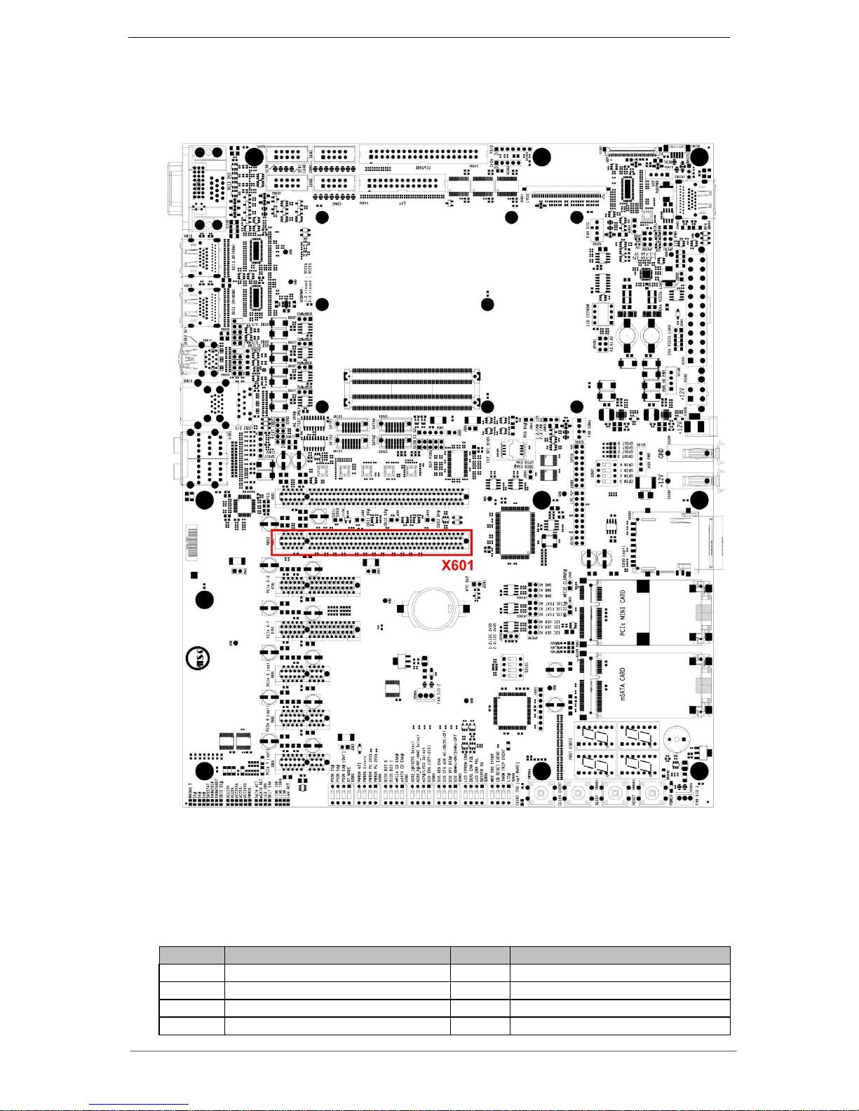
The digital display interfaces can be switched to the ADD2-N (Advanced Digital Display
- Normal) card slot. Refer to chapter 4.42.
Specification:
References: X601
Connector:AMP / Tyco 4-1612163-4
Pin-out: Refer to PCI express specification
Pin
Signal
Pin
Signal
A1
PRSNT1#
B1
12V
A2
12V
B2
12V
A3
12V
B3
12V
A4
GND
B4
GND
Page 27

MSC C6-MB-EVA - PRELIMINARY - User Manual
27 / 63
A5
JTAG_TCK
B5
SMB_CLK
A6
JTAG_TDI
B6
SMB_DAT
A7
JTAG_TDO
B7
GND
A8
JTAG_TMS
B8
3V3
A9
3V3
B9
JTAG_RST#
A10
3V3
B10
3V3_AUX
A11
PE_RST#
B11
WAKE#
KEY
A12
GND
B12
RSVD
A13
REFCLK+ / n.c.
B13
GND
A14
REFCLK- / n.c.
B14
PET_p0 / DDI1 LANE0+
A15
GND
B15
PET_n0 / DDI1 LANE0-
A16
PER_p0 / DDI1 LANE 5+
B16
GND
A17
PER_n0 / DDI1 LANE 5-
B17
PRSNT2# / DDI1 AUX SW+
A18
GND
B18
GND
A19
RSVD
B19
PET_p1 / DDI1 LANE1+
A20
GND
B20
PET_n1 / DDI1 LANE1-
A21
PER_p1 / DDI1 LANE4+
B21
GND
A22
PER_n1 / DDI1 LANE 4-
B22
GND
A23
GND
B23
PET_p2 / DDI1 LANE2+
A24
GND
B24
PET_n2 / DDI1 LANE2-
A25
PER_p2 / DDI1 AUX+
B25
GND
A26
PER_n2 / DDI1 AUX-
B26
GND
A27
GND
B27
PET_p3 / DDI1 LANE3+
A28
GND
B28
PET_n3 / DDI1 LANE3-
A29
PER_p3 / DDI1 HPD
B29
GND
A30
PER_n3 / DDI1 AUX SEL
B30
RSVD
A31
GND
B31
PRSNT2# / DDI1 SW-
A32
RSVD
B32
GND
A33
RSVD
B33
PET_p4 / DDI2 LANE0+
A34
GND
B34
PET_n4 / DDI2 LANE0-
A35
PER_p4 / n.c.
B35
GND
A36
PER_n4 / n.c.
B36
GND
A37
GND
B37
PET_p5 / DDI2 LANE1+
A38
GND
B38
PET_n5 / DDI2 LANE1-
A39
PER_p5 / n.c.
B39
GND
A40
PER_n5 / n.c.
B40
GND
A41
GND
B41
PET_p6 / DDI2 LANE2+
A42
GND
B42
PET_n6 / DDI2 LANE2-
A43
PER_p6 / DDI2 AUX+
B43
GND
A44
PER_n6 / DDI2 AUX-
B44
GND
A45
GND
B45
PET_p7 / DDI2 LANE3+
A46
GND
B46
PET_n7 / DDI2 LANE3-
A47
PER_p7 / DDI2 HPD
B47
GND
A48
PER_n7 / DDI2 AUX SEL
B48
PRSNT2#
A49
GND
B49
GND
A50
RSVD
B50
PET_p8 / DDI3 LANE0+
A51
GND
B51
PET_n8 / DDI3 LANE0-
A52
PER_p8 / n.c.
B52
GND
A53
PER_n8 / n.c.
B53
GND
A54
GND
B54
PET_p9 / DDI3 LANE1+
A55
GND
B55
PET_n9 / DDI3 LANE1-
A56
PER_p9 / n.c.
B56
GND
A57
PER_n9 / n.c.
B57
GND
A58
GND
B58
PET_p10 / DDI3 LANE2+
A59
GND
B59
PET_n10 / DDI3 LANE2-
Page 28
MSC C6-MB-EVA - PRELIMINARY - User Manual
28 / 63
A60
PER_p10 / DDI3 AUX+
B60
GND
A61
PER_n10 / DDI3 AUX-
B61
GND
A62
GND
B62
PET_p11 / DDI3 LANE3+
A63
GND
B63
PET_n11 / DDI3 LANE3-
A64
PER_p11 / DDI3 HPD
B64
GND
A65
PER_n11 / DDI3 AUX SEL
B65
GND
A66
GND
B66
PET_p12 / n.c.
A67
GND
B67
PET_n12 / n.c.
A68
PER_p12 / n.c.
B68
GND
A69
PER_n12 / n.c.
B69
GND
A70
GND
B70
PET_p13 / n.c.
A71
GND
B71
PET_n13 / n.c.
A72
PER_p13 / n.c.
B72
GND
A73
PER_n13 / n.c.
B73
GND
A74
GND
B74
PET_p14 / n.c.
A75
GND
B75
PET_n14 / n.c.
A76
PER_p14 / n.c.
B76
GND
A77
PER_n14 / n.c.
B77
GND
A78
GND
B78
PET_p15 / n.c.
A79
GND
B79
PET_n15 / n.c.
A80
PER_p15 / n.c.
B80
GND
A81
PER_n15 / n.c.
B81
PRSNT2# / n.c.
A82
GND
B82
RSVD
Table 8 Pin out ADD2 Card Slot
Page 29
MSC C6-MB-EVA - PRELIMINARY - User Manual
29 / 63
4.8 VGA Interface
An analog display can be connected via a VGA (VESA DDC) interface.
Specification:
References: X1101
Pin-out: Refer to Table 8
Pin
Signal name
Function
1
RED
Signal red
2
GREEN
Signal green
3
BLUE
Signal blue
4
RSVD
reserved
5
GND
Ground digital
6
RGND
Ground red
7
GGND
Ground green
Page 30
MSC C6-MB-EVA - PRELIMINARY - User Manual
30 / 63
8
BGND
Ground blue
9
+5V
+5V VDC
10
SGND
Ground Synchronisation
11
ID0
Monitor ID Bit 0 (optional)
12
SDA
DDC Data
13
HSYNC
Horizontal Sync.
14
VSYNC
Vertical Sync.
15
SCL
DDC Clock
Table 9 Pin-out VGA Interface
4.9 DVI-D Interface
Specification:
References: X1101
Pin-out: Refer to Table 9
Location: Refer to chapter 4.8 VGA Interface
Pin
Signal name
Function
1
TMDS D2-
T.M.D.S. Data channel 2-
2
TMDS D2+
T.M.D.S. Data channel 2+
3
SHIELD 2/4
Shield connected to Ground
4
TMDS D4- n.c.
reserved
5
TMDS D4+ n.c.
reserved
6
DDC CLK
DDC Clock
7
DDC DATA
DDC Data
8
VSYNC n.c.
Analog Vertical Sync.
9
TMDS D1-
T.M.D.S. Data channel 1-
10
TMDS D1+
T.M.D.S. Data channel 1+
11
SHIELD 1/3
Shield connected to Ground
12
TMDS D3- n.c.
reserved
13
TMDS D3+ n.c.
reserved
14
+5V
+5V VDC
15
GND
Ground
16
HPDET
Hot Plug Detect
17
TMDS D0-
T.M.D.S. Data channel 0-
18
TMDS D0+
T.M.D.S. Data channel 0+
19
SHIELD 0/5
Shield connected to Ground
20
TMDS D5- n.c.
reserved
21
TMDS D5+ n.c.
reserved
22
CLK SHIELD
Clock Shield connected to Ground
23
TMDS CLK+
T.M.D.S. Clock channel -
24
TMDS CLK-
T.M.D.S. Clock channel +
C1
RED n.c.
Analog RED
C2
GREEN n.c.
Analog GREEN
C3
BLUE n.c.
Analog BLUE
C4
HSYNC n.c.
Analog Horizontal Sync.
C5
GND
Analog Ground
Table 10 Pin-out DVI-D Interface
Page 31
MSC C6-MB-EVA - PRELIMINARY - User Manual
31 / 63
4.10 High Definition Multimedia Interface (HDMI)
Specification:
References: X1201, X1301, X3401
Pin-out: Refer to Table 11
Pin
Signal name
Function
1
TMDS D2+
T.M.D.S. Data channel 2+
2
SHIELD 2
Shield connected to Ground
3
TMDS D2-
T.M.D.S. Data channel 2-
4
TMDS D1+
T.M.D.S. Data channel 1+
5
SHIELD 1
Shield connected to Ground
6
TMDS D1-
T.M.D.S. Data channel 1-
7
TMDS D0+
T.M.D.S. Data channel 0+
8
SHIELD 0
Shield connected to Ground
Page 32
MSC C6-MB-EVA - PRELIMINARY - User Manual
32 / 63
9
TMDS D0-
T.M.D.S. Data channel 0-
10
TMDS CLK+
T.M.D.S. Clock channel +
11
CLK SHIELD
Clock Shield connected to Ground
12
TMDS CLK-
T.M.D.S. Clock channel -
13
CEC
n.c. (consumer electronics control)
14
reserved
n.c.
15
DDC CLK
DDC Clock
16
DDC DATA
DDC Data
17
GND
Ground
18
+5V
+5V VDC
19
HPDET
Hot Plug Detect
Table 11 Pin-out HDMI
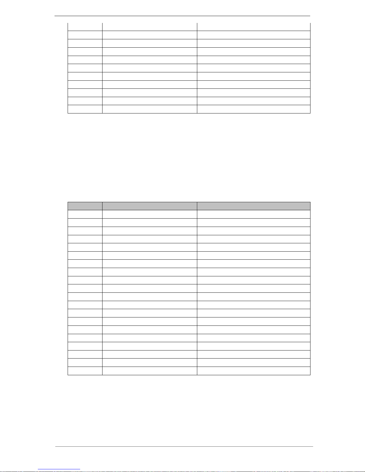
4.11 Display Port (DP)
Specification:
References: X1201, X1301, X3401
Pin-out: Refer to Table 12
Location: Refer to chapter 4.10 High Definition Multimedia Interface (HDMI)
Pin
Signal name
Function
1
LANE 0 +
LANE 0 positive data signal
2
GND
Ground
3
LANE 0 -
LANE 0 negative data signal
4
LANE 1 +
LANE 1 positive data signal
5
GND
Ground
6
LANE 1 -
LANE 1 negative data signal
7
LANE 2 +
LANE 2 positive data signal
8
GND
Ground
9
LANE 2 -
LANE 2 negative data signal
10
LANE 3 +
LANE 3 positive data signal
11
GND
Ground
12
LANE 3 -
LANE 3 negative data signal
13
CONFIG1
CA_DET (cable detect)
14
CONFIG2
Ground
15
AUX CH +
Auxiliary Channel positive signal
16
GND
Ground
17
AUX CH -
Auxiliary Channel negative signal
18
HPDET
Hot Plug Detect
19
Return
Ground
20
DP_PWR
+3,3 VDC
Table 12 Pin-out Display Port
Page 33
MSC C6-MB-EVA - PRELIMINARY - User Manual
33 / 63
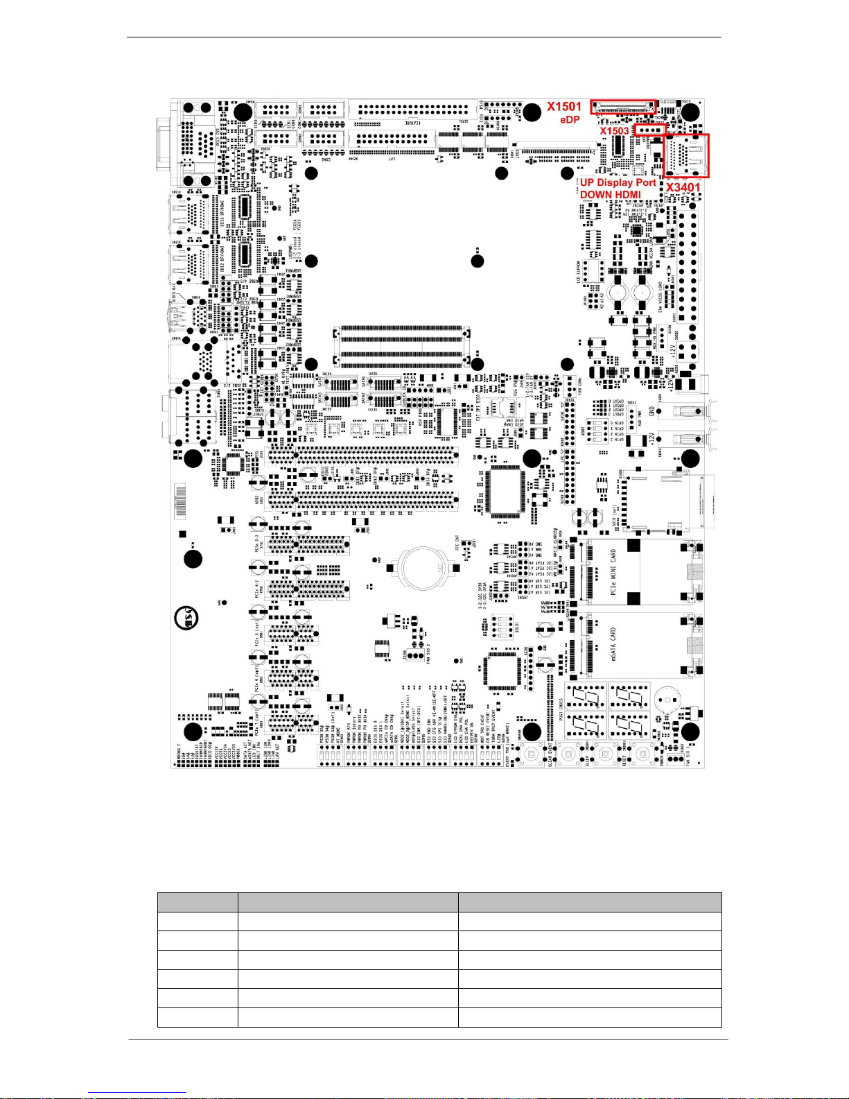
4.12 Embedded Display Port (eDP)
Specification:
References: X1501
Connector:Tyco 5-2069716-3, I-PEX 20455-040E-02
Pin-out: Refer to Table 13
Pin
Signal name
Function
1
RSVD
Reserved for LCD manufacturer’s use
2
BL_PWR
Backlight power
3
BL_PWR
Backlight power
4
BL_PWR
Backlight power
5
BL_PWR
Backlight power
6
RSVD
SMBDAT
Page 34

MSC C6-MB-EVA - PRELIMINARY - User Manual
34 / 63
7
RSVD
SMBCLK
8
BL_PWM_DIM or NC
System PWM signal input for dimming
(Optional)
9
BL_ENABLE or NC
Backlight On/0ff (Optional)
10
BL_GND
Backlight ground
11
BL_GND
Backlight ground
12
BL_GND
Backlight ground
13
BL_GND
Backlight ground
14
HPD
Hot Plug Detect
15
LCD_GND
LCD logic and driver ground
16
LCD_GND
LCD logic and driver ground
17
LCD_GND
LCD logic and driver ground
18
LCD_GND
LCD logic and driver ground
19
LCD_Self_Test or NC
LCD Panel Self Test Enable n.c.
20
LCD_VCC
LCD logic and driver power
21
LCD_VCC
LCD logic and driver power
22
LCD_VCC
LCD logic and driver power
23
LCD_VCC
LCD logic and driver power
24
H_GND
High Speed Ground
25
AUX_CH_N
Auxiliary Channel negative signal
26
AUX_CH_P
Auxiliary Channel positive signal
27
H_GND
High Speed Ground
28
Lane0_P
LANE 0 positive data signal
29
Lane0_N
LANE 0 negative data signal
30
H_GND
High Speed Ground
31
Lane1_P
LANE 1 positive data signal
32
Lane1_N
LANE 1 negative data signal
33
H_GND
High Speed Ground
34
Lane2_P
LANE 2 positive data signal
35
Lane2_N
LANE 2 negative data signal
36
H_GND
High Speed Ground
37
Lane3_P
LANE 3 positive data signal
38
Lane3_N
LANE 3 negative data signal
39
H_GND
High Speed Ground
40
RSVD
Reserved for LCD manufacturer’s use
Table 13 Pin-out embedded Display Port
The supply voltage of the eDP backlight can be adjusted with jumper JP1702. The according
position is printed on the PCB. Refer to chapter 4.14 LVDS-Interface.
Also the voltage can supplied with X1503. If this option is used leave jumper JP1702 open.
Specification eDP Backlight Power Supply:
References: X1503
Connector:AMP 171825-4
Location: Refer to chapter 4.12 Embedded Display Port (eDP)
Pin
Function
1
+12V
2
GND
3
GND
4
PWRBL
Table 14 Pin-out eDP Backlight Power Supply Connector
Page 35
MSC C6-MB-EVA - PRELIMINARY - User Manual
35 / 63
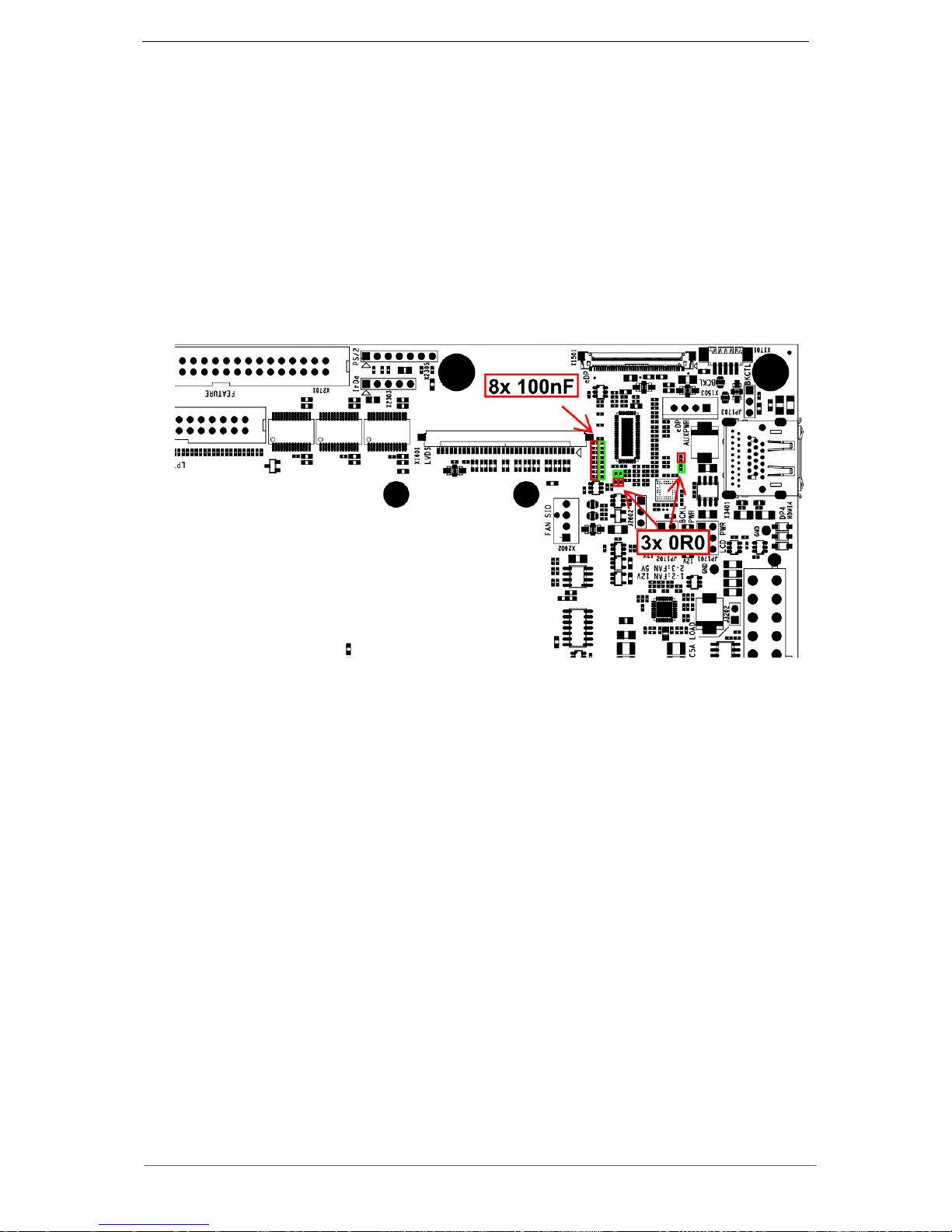
4.13 Alternative Embedded Display Port and HDMI Connector
The selection of these connectors is described in chapter 4.42
Specification:
References: X3401
Pin-out: Refer to Table 12 and Table 13
Location: Refer to chapter 4.12 Embedded Display Port (eDP)
To change DP signals lanes from eDP connector to X3401 remove red parts and replace them at
green locations:
Page 36
MSC C6-MB-EVA - PRELIMINARY - User Manual
36 / 63
4.14 LVDS-Interface
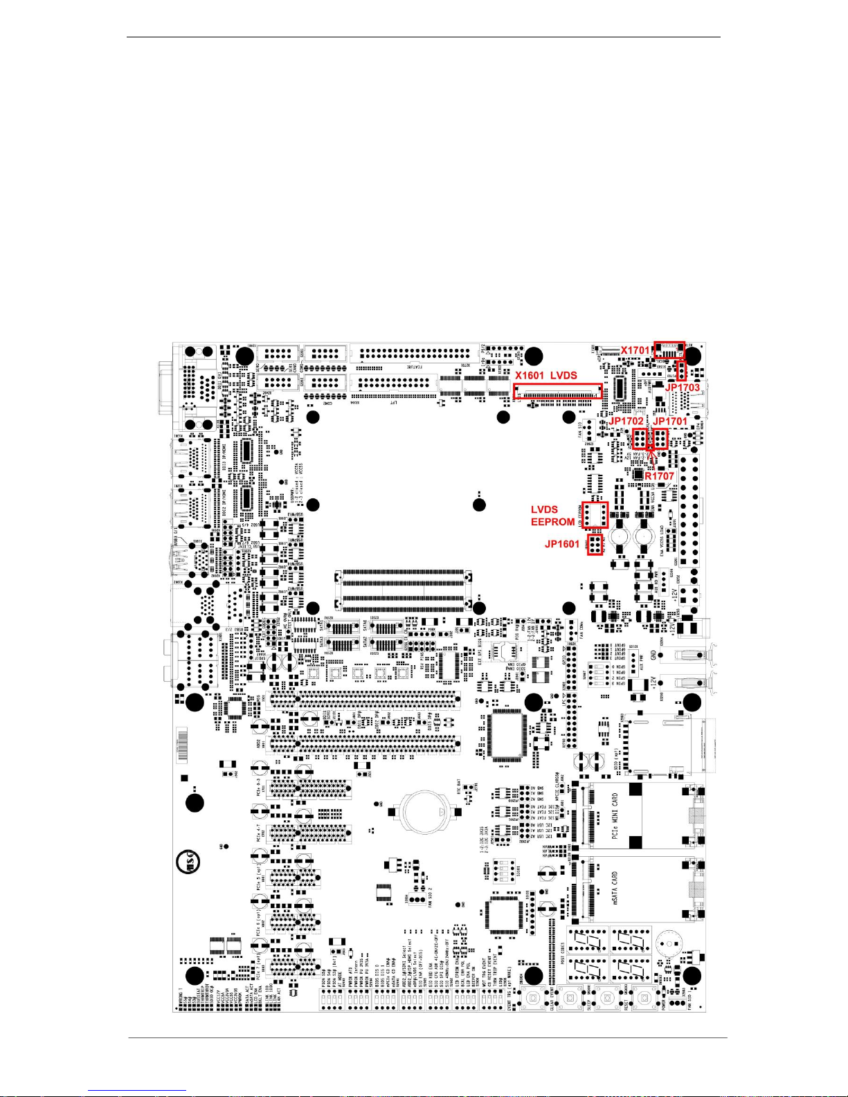
Any LCD display can be connected via a JILI30 connector.
Two 24 bit LVDS channels are present on this 30-pin connector.
The supply voltage of the display can be adjusted with jumper JP1701. The according position is
printed on the PCB. +12V supply voltage is only available with setting R1707 (0R0).
If the display needs a low active start signal VDD_EN, DIP-Switch S2906 #2 has to be set open.
If the display needs a high active start signal VDD_EN, DIP-Switch S2906 #2 has to be set on.
Specification:
References: X1601
Connector:JAE FI-X30SSL-HF
Pin-out: Refer to Table 15 "JILI30" according to JILI specification [4]
Page 37
MSC C6-MB-EVA - PRELIMINARY - User Manual
37 / 63
Pin
Signal name
Function
1
LVDS_A0-
LVDS Negative data signal (-)
2
LVDS_A0+
LVDS Positive data signal (+)
3
LVDS_A1-
LVDS Negative data signal (-)
4
LVDS_A1+
LVDS Positive data signal (+)
5
LVDS_A2-
LVDS Negative data signal (-)
6
LVDS_A2+
LVDS Positive data signal (+)
7
VSS
Ground
8
LVDS_A_CK-
LVDS Negative clock signal (-)
9
LVDS_A_CK+
LVDS Positive clock signal (+)
10
LVDS_A3-
LVDS Negative data signal (-)
11
LVDS_A3+
LVDS Positive data signal (+)
12
LVDS_B0-
LVDS Negative data signal (-)
13
LVDS_B0+
LVDS Positive data signal (+)
14
VSS
Ground
15
LVDS_B1-
LVDS Negative data signal (-)
16
LVDS_B1+
LVDS Positive data signal (+)
17
VSS
Ground
18
LVDS_B2-
LVDS Negative data signal (-)
19
LVDS_B2+
LVDS Positive data signal (+)
20
LVDS_B_CK-
LVDS Negative clock signal (-)
21
LVDS_B_CK+
LVDS Positive clock signal (+)
22
LVDS_B3-
LVDS Negative data signal (-)
23
LVDS_B3+
LVDS Positive data signal (+)
24
GND
Ground
25
LVDS I2C DAT
I²C Data
26
VDD EN
Display power enable signal
27
LVDS I2C CK
I²C Clock
28
VCC LCDSW
Switched Power Supply
(Voltage depend on JP1701)
29
VCC LCDSW
Switched Power Supply
(Voltage depend on JP1701)
30
VCC LCDSW
Switched Power Supply
(Voltage depend on JP1701)
Table 15 Pin-out JILI30 LVDS-Interface
4.14.1 LVDS EEPROM Socket
A serial EEPROM is connected to the signals LVDS_I2C_CK and LVDS_I2C_DAT to store
configuration data of the LCD.
This EEPROM can be assembled optionally or it can be disabled with a closed DIP-Switch S2906
#4 to avoid conflicts with configuration EEPROM connected via the JILI connector.
Specification:
References: U1601
Connector: DIP8 socket
Pin-out: Refer to Table 16
Location: Refer to chapter 4.14 LVDS-Interface
Page 38
MSC C6-MB-EVA - PRELIMINARY - User Manual
38 / 63
Pin
Signal name
Function
1
A0
EEPROM Address 0 (PD 10k)
2
A1
EEPROM Address 1 (PD 10k)
3
A2
EEPROM Address 2 (PD 10k)
4
GND
Ground
5
SDA
Serial data
6
SCL
Serial clock
7
WP
Write protection (Ground, disabled)
8
VCC
Power supply 3V3
Table 16 Pin-out LVDS EEPROM Socket
The LVDS EEPROM address can be select with the nearby jumper block JP1601. To
use this option, the pull-up resistors must be assembled.
Pin
Signal name
Function
1-2
A0
EEPROM Address 0 connect to GND
3-4
A1
EEPROM Address 1 connect to GND
5-6
A2
EEPROM Address 2 connect to GND
Table 17 EEPROM Address JP1601
4.14.2 Backlight Inverter Interface
The supply voltage of the backlight can be adjusted with jumper JP1702. The according position
is printed on the PCB.
DIP switch S2906 #2 should be set according to the backlight inverter used.
If the inverter needs a low active start signal, DIP-Switch S2906 #3 has to be set open.
If the inverter needs a high active start signal, DIP-Switch S2906 #3 has to be set on.
Brightness of the backlight inverter is controlled via the LVDS-BKLT-CTRL signal.
The LVDS-BKLT-CTRL signal of the COM Express module is a PWM signal with current
chipsets. If jumper JP1703 is placed between pins 1-2, the signal is integrated and then limited to
the maximum allowable voltage of the backlight inverter via a voltage divider. If the jumper
JP1703 is closed between pins 2-3, the LVDS-BKLT-CTRL signal of the COM Express module is
routed straight to the backlight inverter connector.
Control voltage: 0...3V
A value of 0V corresponds to maximum brightness.
Specification:
References: X1701
Connector:Molex (53047-0510) 53261-0590
Pin-out: Refer to Table 18
Location: Refer to chapter 4.14 LVDS-Interface
Pin
Signal name
Function
1
VCC
Power supply backlight
2
GND
Ground
3
BLON#
Backlight On
4
VCON
Brightness control
5
GND
Ground
Table 18 Pin-out Backlight
Page 39
MSC C6-MB-EVA - PRELIMINARY - User Manual
39 / 63
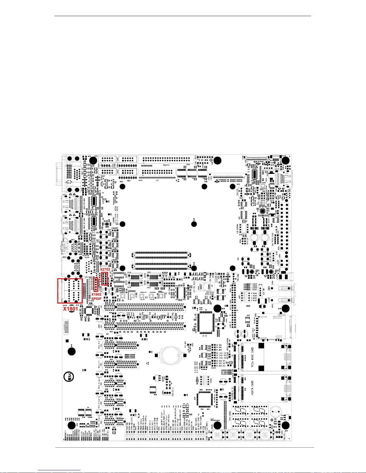
4.15 Audio
A Realtek ALC888 HD audio codec is connected to the AC link of the COM Express module.
Following LF signals are provided by the HDA codec:
Stereo LineIn
Stereo LineOut
Stereo Microfon
Mono Center / Mono LFE
Stereo Surround
Stereo Side
Note: At rev. 3 carrier (LY30E801) some COM Express modules can have problems with the delay of
the signal multiplexers U1802 and U1803 (74HCT4053).
A corrective action is to replace the multiplexers by copper wire.
Page 40
MSC C6-MB-EVA - PRELIMINARY - User Manual
40 / 63
4.15.1 HDA Connector
Specification:
References: X1801
Connector:Foxconn JAS331-H1G2-4F
Pin-out: Refer to Table 19
Location: Refer to chapter 4.15 Audio
Con
Color
Function
1
light blue
Line In
2
lime
Line Out
3
pink
Mikrofon
4
orange
Center / LFE
5
black
Surround
6
grey
Side
Table 19 Pin-out LineOut
4.15.2 SPDIF
The ALC888 SPDIF signals are routed to a pin header.
Specification:
References: X1802
Connector:Pin header (5 pins)
Pin-out: Refer to Table 20
Location: Refer to chapter 4.15 Audio
Pin
Signal name
Function
1
VCC
+5V Power Supply
2
SPDIF IN
Signal input
3
SPDIF OUT
Signal output
4
GND
Ground
5
NC
Not connected
Table 20 Pin-out SPDIF
4.15.3 HDA Codec Adapter (not available from Rev.4)
The AC link signals can be switched to a 10 pin header.
The SDIN0-2 signals can be select via resistors R2701 (SDIN0, default), R2702 (SDIN1) and
R2703 (SDIN2)
A low level at EN_EXT_HDA# switches the signals to the pin header.
Specification:
References: X2702
Connector:Pinheader 5x2
Pin-out: Refer to Table 21
Location: Refer to chapter 4.15 Audio
Pin
Signal
Signal
Pin
1
+12V
+3,3V
2
3
HAD_SYNC
HAD_RST#
4
5
HAD_SDIN0/1/2
HAD_BIT_CLK
6
7
HAD_SDOUT
EN_EXT_HDA#
8
9
GND
GND
10
Table 21 Pin-out HAD Codec Adapter
Page 41
MSC C6-MB-EVA - PRELIMINARY - User Manual
41 / 63
4.16 SATA-Interface
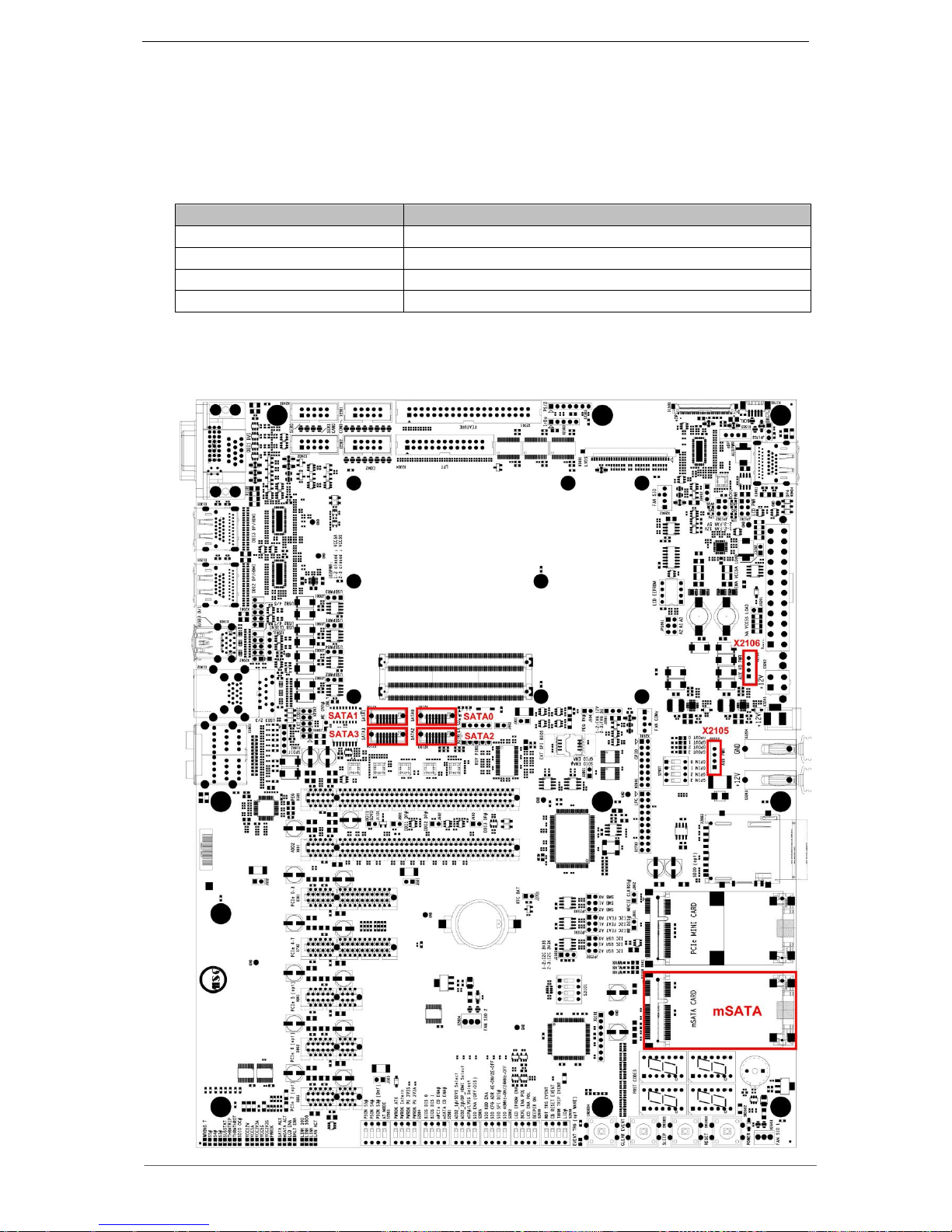
Up to four SATA drives can be connected to the SATA interfaces.
Note: Depending on the COM Express module used, not all SATA ports are available.
For disk drive power there is one power supply connector available.
SATA Channel
References
SATA 0
X2101
SATA 1
X2102
SATA 2
X2103
SATA 3
X2104 (multiplexed with mSATA socket)
Table 22 Assignment SATA Channel to Connector Reference
Page 42
MSC C6-MB-EVA - PRELIMINARY - User Manual
42 / 63
Specification:
References: X2101, X2102, X2103, X2104
Connector:FCI 10035691
Pin-out: Refer to Specification SATA [8, page 46, table 3]
Specification Power Supply:
References: X2105, X2106
Connector:AMP 171825-4
Pin-out: Refer to ATX specification V2.2 [2, "Floppy Drive Power Connector"]
Location: Refer to chapter 4.16 SATA-Interface
4.17 mSATA Interface
One mSATA slot is available at the C6-MB-EVA board. The SATA channel is shared
with SATA 3 port. It will be automatically switched if an mSATA card is plugged in. It can
also be selected with DIP switch 1 at S2901.
Specification:
References: X2109
Connector:Molex 67910-9000
Pin-out: Refer to Table 22
Location: Refer to chapter 4.16 SATA-Interface
Pin
Signal
Pin
Signal
1
Not connected
2
+3,3V
3
Not connected
4
GND
5
Not connected
6
+1,5V
7
Not connected
8
Not connected
9
GND
10
Not connected
11
Not connected
12
Not connected
13
Not connected
14
Not connected
15
GND
16
Not connected
17
Not connected
18
GND
19
Not connected
20
Not connected
21
GND
22
Not connected
23
mSATA_RX-
24
+3,3V
25
mSATA_RX+
26
GND
27
GND
28
+1,5V
29
GND
30
SMB_CLK
31
mSATA_TX-
32
SMB_DAT
33
mSATA_TX+
34
GND
35
GND
36
Not connected
37
GND
38
Not connected
39
+3,3V
40
GND
41
+3,3V
42
Not connected
43
PD not populated
44
Not connected
45
Not connected
46
Not connected
47
Not connected
48
+1,5V
49
mSATA_ACT#
50
ENAUTO_mSATA#
51
Not connected
52
+3,3V
Table 23 Pin-out mSATA socket
Page 43
MSC C6-MB-EVA - PRELIMINARY - User Manual
43 / 63
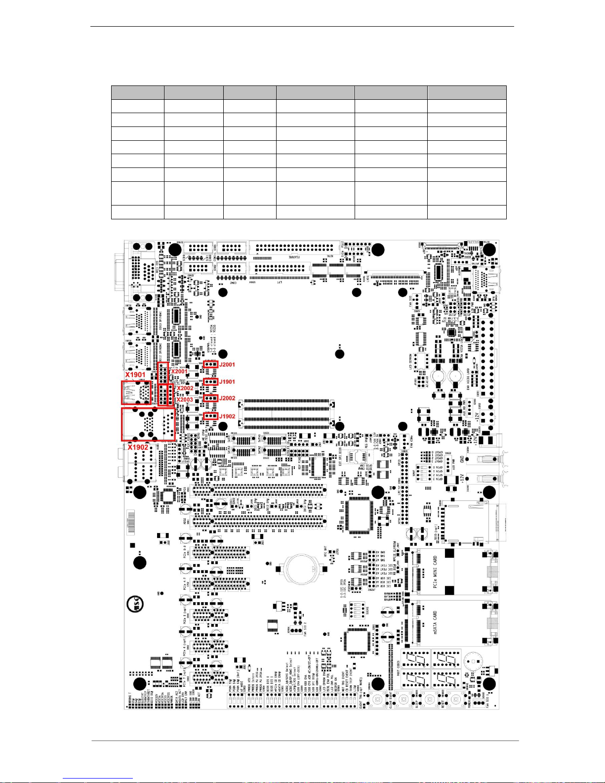
4.18 USB Topology
Eight USB ports are normally provided by the COM Express module.
The exact assignment of each port is defined in the following table:
USB-Port
References
Function
Location
Power jumper
Remarks
USB0
X1901
USB 3.0
I/O Shield
J1901
USB1
X1901
USB 3.0
I/O Shield
J1901
USB2
X1902
USB 3.0
I/O Shield
J1902
With RJ45
USB3
X1902
USB 3.0
I/O Shield
J1902
With RJ45
USB4
X2001
USB 2.0
Internal header
J2001
USB5
X2001
USB 2.0
Internal header
J2001
USB6
X2002
USB 2.0
Internal header
J2002
Shared with
PCIe Mini Card
USB7
X2002
USB 2.0
Internal header
J2002
Table 24 Assignment USB Ports
Page 44
MSC C6-MB-EVA - PRELIMINARY - User Manual
44 / 63
4.18.1 USB Power Supply
The power supplies are protected by USB power switches. With power jumper setting the USB
power can be sourced from standard +5V (2-3) or from suspend +5V (1-2).
The USB power switches have the following functions:
The output current is limited to 500mA at each USB 2.0 port and 800mA at each USB
3.0 port
A signal to detect over-current is generated for each two ports
USB0 and USB1 have one common signal to detect over-current
USB2 and USB3 have one common signal to detect over-current
USB4 and USB5 have one common signal to detect over-current
USB6 and USB7 have one common signal to detect over-current
4.18.2 USB Connectors
Specification:
References: X1901
Connector:Foxconn UEA1112C-8HS1-4F (Dual USB 3.0 connector type A)
Pin-out: according to USB specification 3.0 [10]
Location: Refer to chapter 4.18 USB Topology
References: X1902
Connector:Würth 749110616 (RJ45LAN 10/100/1000 BaseT + USB 3.0)
Pin-out: according to USB specification 3.0 [10]
Location: Refer to chapter 4.18 USB Topology
References: X2001, X2002
Connector:Pinheader 5x2
Pin-out: Refer to Table 25 and Table 26
Location: Refer to chapter 4.18 USB Topology
Pin
Signal
Pin
Signal
1
VCC_USB4
2
VCC_USB5
3
USB_P4_N
4
USB_P5_N
5
USB_P4_P
6
USB_P5_P
7
GND
8
GND
9
Not connected
10
key
Table 25 Pin-out USB 2.0 pin header
Pin
Signal
Pin
Signal
1
VCC_USB6
2
VCC_USB7
3
USB_P6_N
4
USB_P7_N
5
USB_P6_P
6
USB_P7_P
7
GND
8
GND
9
Not connected
10
key
Table 26 Pin-out USB 2.0 pin header
Note: At Rev.1 carrier (LY10E801) the Pin1 at X2001 and pin1 at X2002 are on opposite sides in the
layout.
Page 45
MSC C6-MB-EVA - PRELIMINARY - User Manual
45 / 63
4.18.3 USB Client Connector
The USB Port 7 signals were switched to a 5 pin header, if a USB client is plugged at X2003.
The client control signal is routed to an auxiliary header X2705 at pin 2.
Specification:
References: X2003
Connector:single row pin header
Pin-out: Refer to Table 27
Location: Refer to chapter 4.18 USB Topology
Pin
Signal
Function
1
VCC_IN_CLIENT
Power in
2
USB_P7_N
USB port 7 negative signal
3
USB_P7_P
USB port 7 positive signal
4
GND
Power Ground
5
GND_SHLD
Ground Shield
Table 27 USB Client Connector
4.19 Ethernet
The base board can be connected to a local area network with an Ethernet interface. The COM
Express module already provides MDI signals, so that only the transformer on the base board
required. The transformer is integrated in X1902.
Specification:
References: X1902
Connector:Würth 749110616 (RJ45LAN 10/100/1000 BaseT + USB 3.0)
Pin-out: Refer to IEEE Std. 802.3
[9, section three, page 225]
Location: Refer to chapter 4.18 USB Topology
Color
Status
Description
Yellow
Off
No link
Yellow
Blinking
Link established, activity detected
Green/Orange
Off
10 Mbps
Green
On
100 Mbps
Orange
On
1000 Mbps
LAN LED Description
4.20 LPC Connector
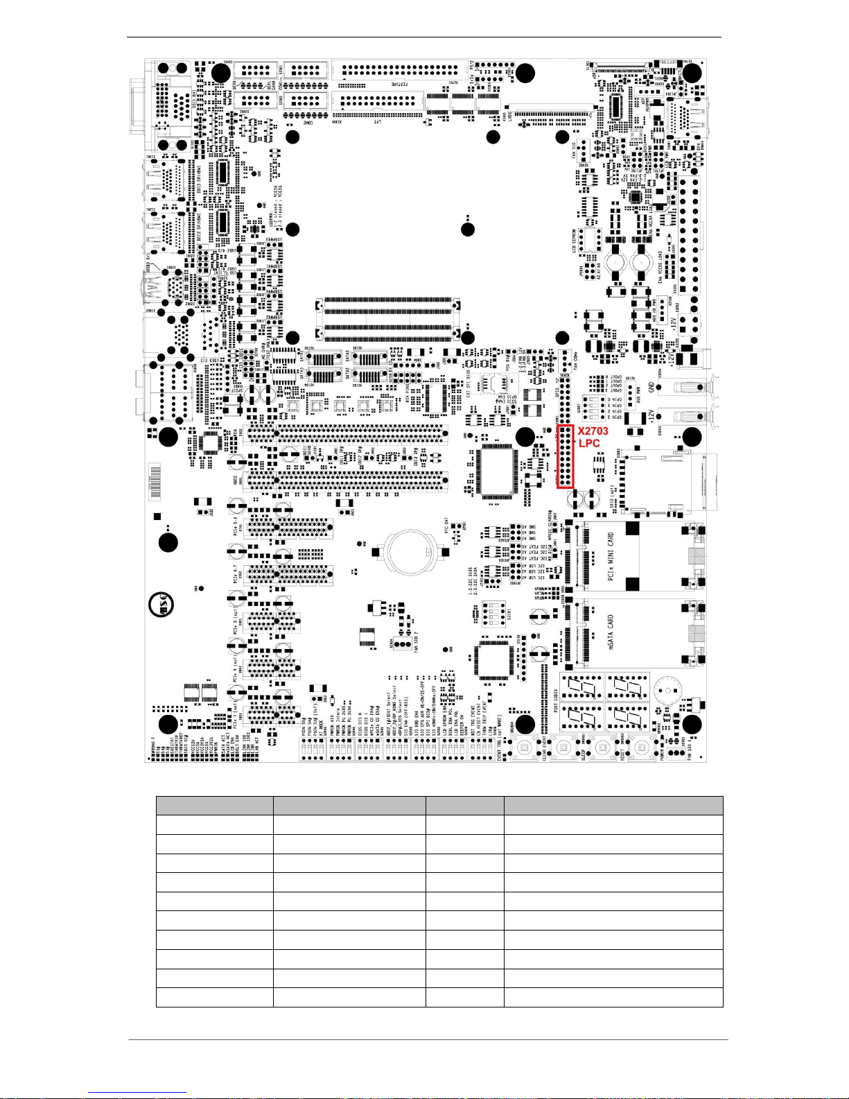
The LPC signals are available on a pin header.
Specification:
References: X2703
Connector:20 pin header, 2.54mm
Pin-out: Refer to Table 28
Page 46
MSC C6-MB-EVA - PRELIMINARY - User Manual
46 / 63
Pin
Signal
Pin
Signal
1
LPC_CLK
2
GND
3
LPC_FRAME#
4
NC
5
LPC_RST#
6
VCC5V_SUS
7
LPC_LAD3
8
LPC_LAD2
9
VCC3V3_SBY
10
LPC_LAD1
11
LPC_LAD0
12
GND
13
SMB_CLK
14
SMB_DAT
15
VCC3V3
16
SERIRQ
17
GND
18
NC
19
PM_SUS_STAT#
20
LPC_DRQ1#
Table 28 Pin-out LPC-Slot
Page 47
MSC C6-MB-EVA - PRELIMINARY - User Manual
47 / 63
4.21 GPIO
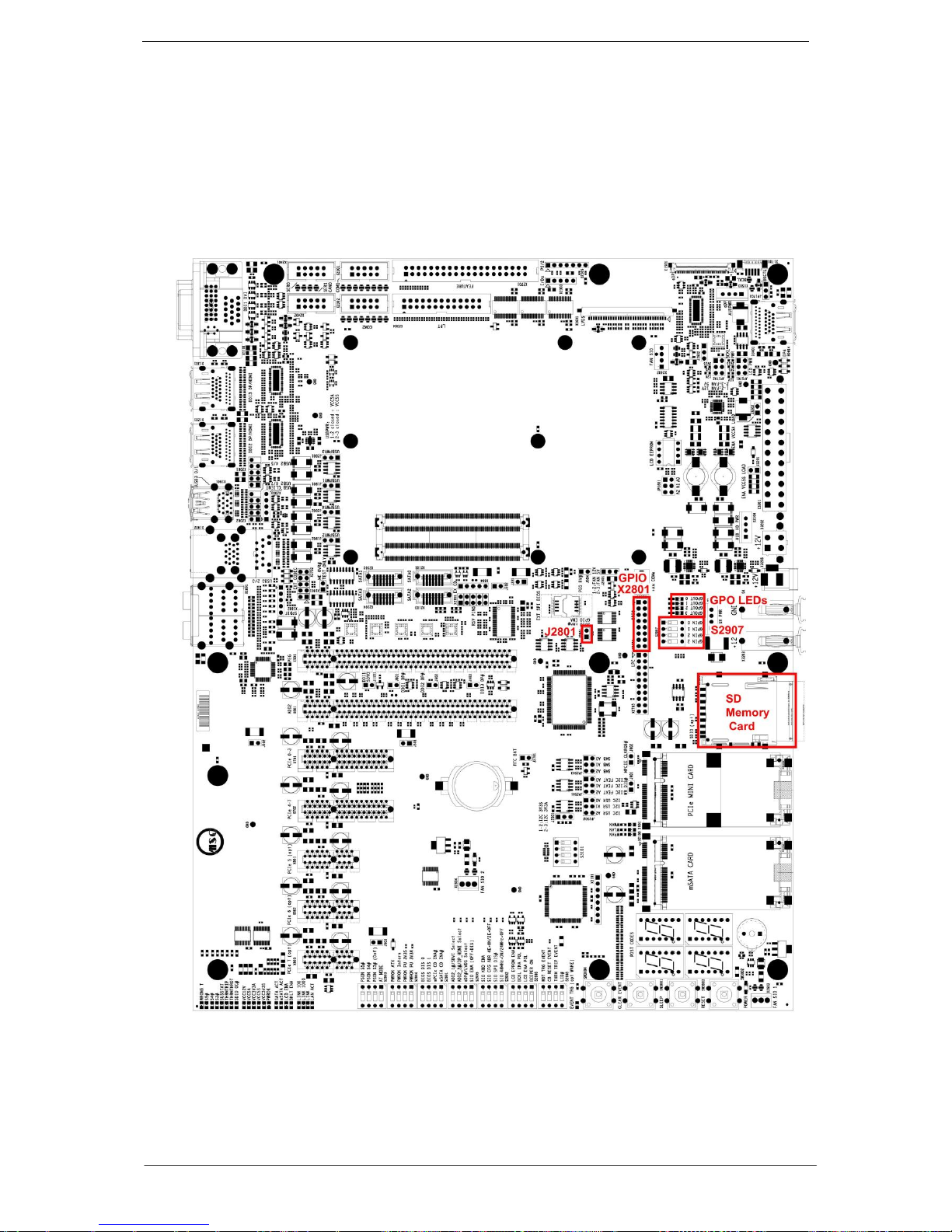
The COM Express module provides four general purpose outputs and four general purpose
inputs.
The GPIs have pull-up resistors and are routed to a dip switch (S2907). With the dip switch the
GPIs can be connected to ground. The assignment GPI – switch – level is printed on the PCB.
From rev.4 the GPI signals cannot be switched to SD Card port.
The GPOs are connected to LEDs for optically status display.
Page 48
MSC C6-MB-EVA - PRELIMINARY - User Manual
48 / 63
4.21.1 GPIO Connector
Don’t set jumper J2801 to use the GPI signals at X2801. (Default)
Specification:
References: X2801
Connector:16 pin header, 2.54mm
Pin-out: Refer to Table 29
Pin
Signal
Pin
Signal
1
GPI0
2
GND
3
GPI1
4
GND
5
GPI2
6
GND
7
GPI3
8
GND
9
GPO0
10
GND
11
GPO1
12
GND
13
GPO2
14
GND
15
GPO3
16
GND
Table 29 Pin-out GPIO connector
4.21.2 SD Memory Card Connector
An SD memory card connector is available on the board.
Set J2801 to enable the SD memory card slot.
All signals at DIP-switch S2907 must be set off for correct function of the SD memory card slot.
This sanction concerns layout revision 3 (LY30E801) and earlier.
Specification:
References: X2803
Connector:Hirose DM1AA-SF-PEJ
Pin-out: Refer to SD Specification [11]
4.22 COM Ports COM3 COM4
Characteristics of the COM ports:
RS232 standard
RS232 transceiver ESD protected +/- 15kV
EMC improved by using EMI filters in the signal lines
Specification:
References: X2401 (COM3), X2402 (COM4)
Connector:10 pin IDC-M
Pin-out: Refer to Table 30
Location: Refer to chapter 4.23 Super IO
Pin
Signal
Function
Function
Signal
Pin
1
DCD#
n.c.
n.c.
DSR#
2
3
RXD
Receive Data
n.c.
RTS#
4
5
TXD
Transmit Data
n.c.
CTS#
6
7
DTR#
n.c.
n.c.
RI#
8
9
GND
Ground
n.c.
VCC
10
Table 30 Pin-out COM Ports
Page 49
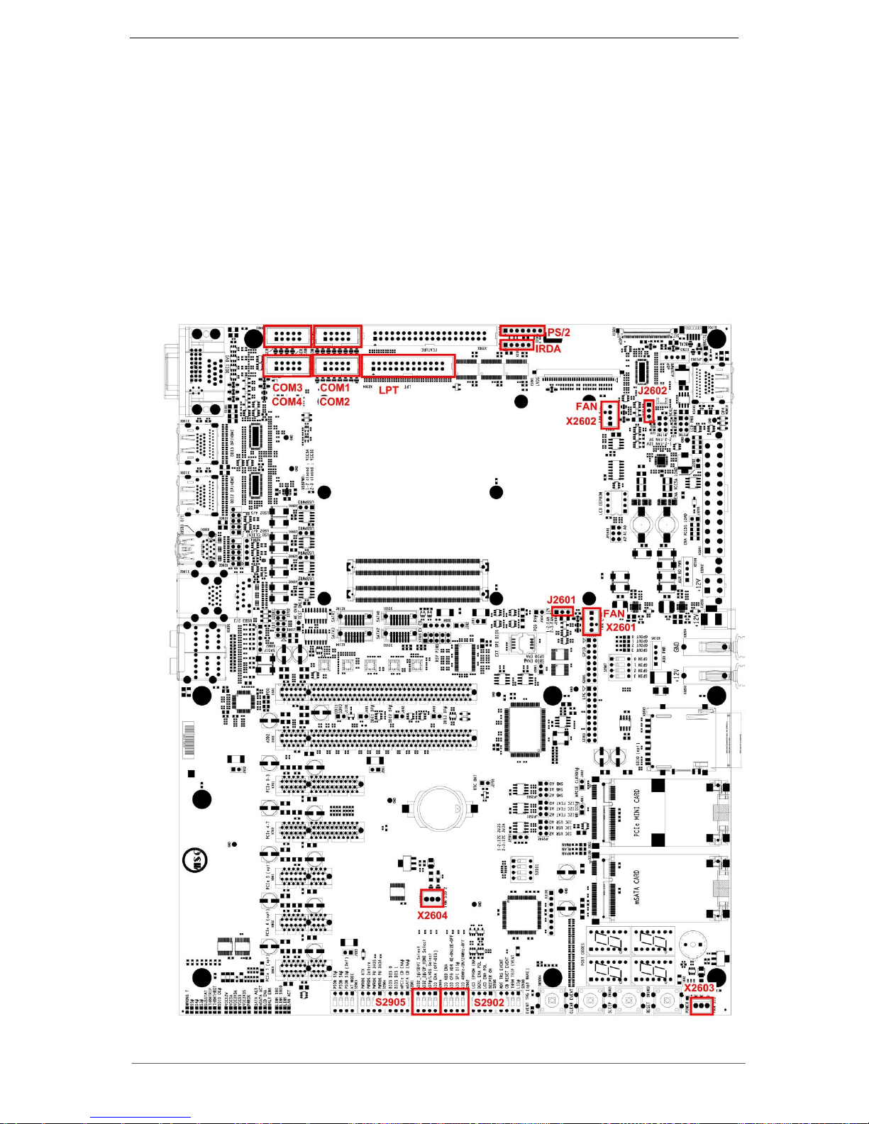
MSC C6-MB-EVA - PRELIMINARY - User Manual
49 / 63
4.23 Super IO
The Winbond Super IO W83627HG is integrated on the base board.
Interfaces used by the Super IO
2 RS232 interface (function of COM port shared with IrDA interface)
1 IrDA interface (function shared with COM port)
1 LPT interface
PS/2 interface for keyboard and mouse
2 fan interfaces
4 voltage monitors
2 temperature sensors
Page 50
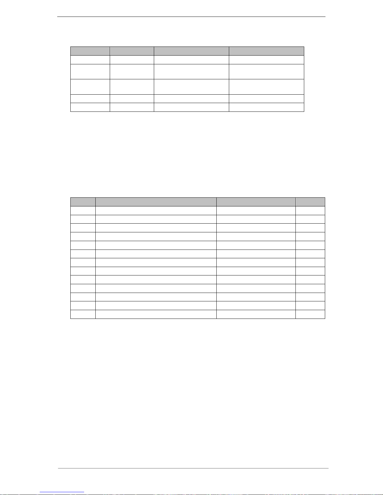
MSC C6-MB-EVA - PRELIMINARY - User Manual
50 / 63
4.23.1 SIO Configuration
The SIO strap options can be changed via DIP switches S2902 and S2905.
Switch
Signal name
ON
OFF
S2902 #1
48MHz_EN
Enable 48MHz (default)
Enable 24MHz
S2902 #2
PNP_ADR
Reset FDC UARTs LPT
setting
No reset FDC UARTs
LPT setting
S2902 #3
4EH_ENA
SIO address 4EH
(default)
SIO address 2EH
S2902 #4
KBD_EN
Enable KBC
Disable KBC
S2905 #1
SIO_RST_N
Enable SIO
Disable SIO
Table 31 SIO Configuration
4.23.2 Parallel Port
Specification:
References: X2304
Connector:26 pin IDC-M
Pin-out: Refer to Table 32
Pin
Signal name
Signal name
Pin
1
STB#
AFD#
2
3
PD0
ERR#
4 5 PD1
INIT#
6
7
PD2
SLIN#
8
9
PD3
GND
10
11
PD4
GND
12
13
PD5
GND
14
15
PD6
GND
16
17
PD7
GND
18
19
ACK#
GND
20
21
BUSY
GND
22
23
PE
GND
24
25
SLCT
VCC n.c.
26
Table 32 Pin-out LPT Port
4.23.3 COM Ports COM1 COM2
Characteristics of the COM ports:
RS232 standard
RS232 transceiver ESD protected +/- 15kV
EMC improved by using EMI filters in the signal lines
Specification:
References: X2301 (COM1), X2302 (COM2)
Connector:10 pin IDC-M
Pin-out: Refer to Table 33 Pin-out COM Ports
Page 51
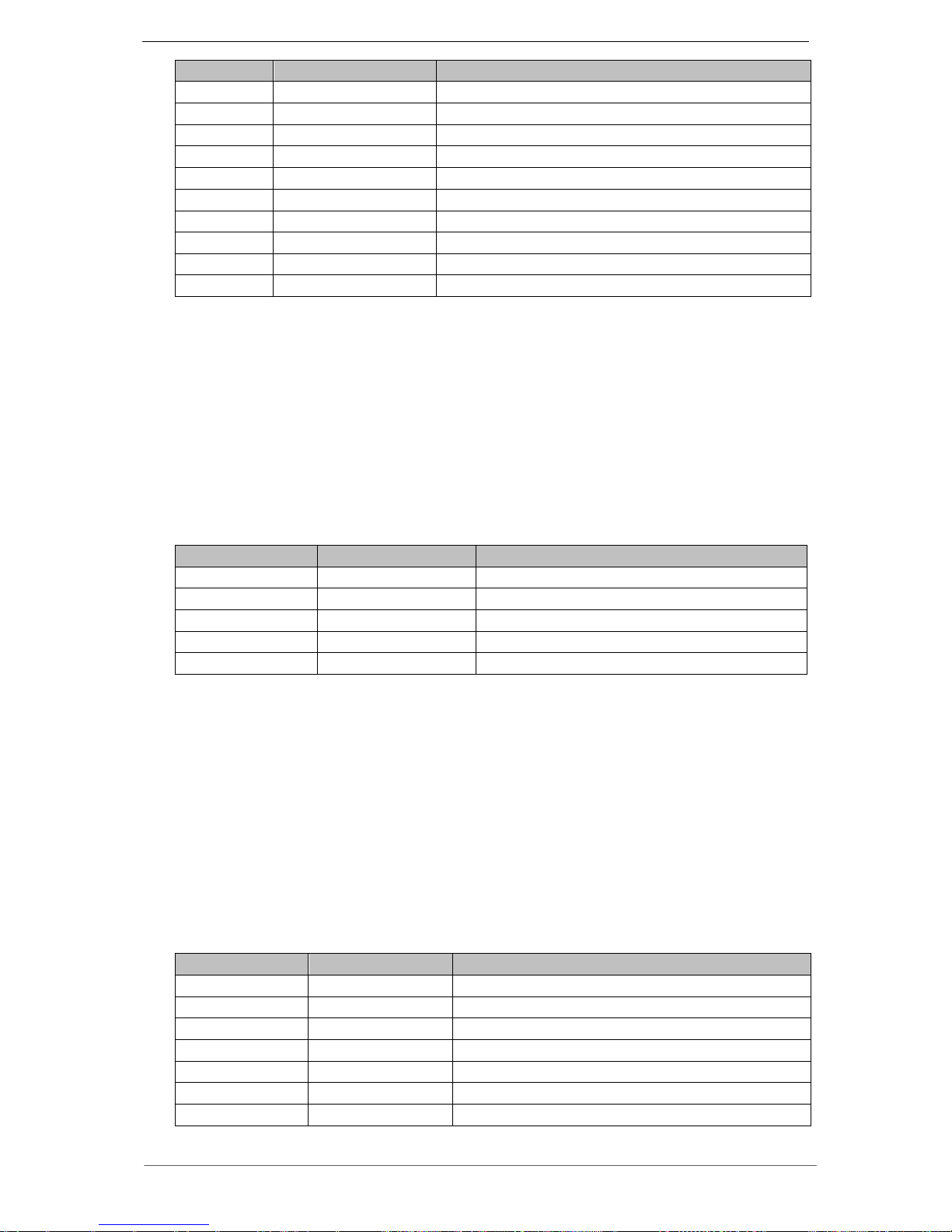
MSC C6-MB-EVA - PRELIMINARY - User Manual
51 / 63
Pin
Signal name
Function
1
DCD#
Data Carrier Detect
2
DSR#
Data Set Ready
3
RXD
Receive Data
4
RTS#
Request To Send
5
TXD
Transmit Data
6
CTS#
Clear To Send
7
DTR#
Data Terminal Ready
8
RI#
Ring Indicator
9
GND
Ground
10
VCC
n. c.
Table 33 Pin-out COM Ports
4.23.4 IrDA
The connectors of the IrDA interface are designed for commercial IrDA transmitters.
Specification:
References: X2303
Connector:CAB 1001-161-005
Pin-out: Refer to Table 34
Pin
Signal name
Function
1
+5V
Power supply
2
NC
Not connected
3
IRRX
Received data
4
GND
Ground
5
IRTX
Transmission data
Table 34 Pin-out IrDA
4.23.5 PS/2 Connector
The PS/2 signals are routed to a 7pin single row header to connect PS/2 keyboards and PS/2
mice.
Specification:
References: X2305
Connector:7 pin single row header 2.54mm
Pin-out: Refer to Table 35
Pin
Signal name
Function
1
KBDAT
Keyboard Data
2
NC
not connected
3
MSDAT
Mouse Data
4
GND
Ground
5
+5V
VCC
6
KBCLK
Keyboard Clock
7
MSCLK
Mouse Clock
Table 35 Pin-out PS/2 Connector
Page 52
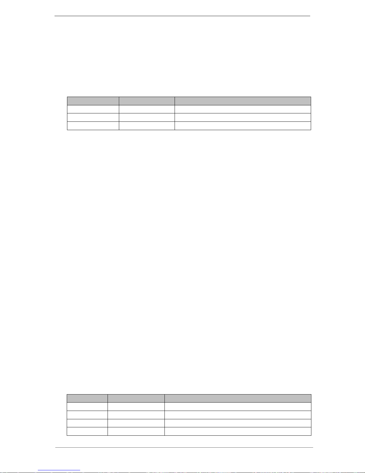
MSC C6-MB-EVA - PRELIMINARY - User Manual
52 / 63
4.23.6 Super IO Fan interface
Two PWM controlled fan interfaces are integrated on the base board.
Measurement of the tacho signal and control of the rotation speed is done by the Super IO.
Specification:
References: X2603, X2604
Connector:Molex 22-04-1031
Pin-out: Refer to Table 36
Pin
Signal name
Function
1
GND
Ground
2
PWM
PWM signal
3
TACHO
Tacho signal
Table 36 Pin-out SIO Fan Interface
4.23.7 Super IO Hardware Monitor
Various voltages and temperatures can be monitored by hardware integrated in the SuperIO.
Monitored voltages
3.3V
12V
Output voltage from CX 12V Vin current sensor (OP)
Output voltage from CX 5V STBY Vin current sensor (OP)
Measured temperatures
2 ambient temperatures
Temperature is measured with a thermistor.
4.24 Fan Interface
4.24.1 Intel Fan interface
In addition to the two fan interfaces according to Super IO, there is the X2601intel fan
connector on the board which is supported from COM Express interface.
The second intel fan interface at X2602 is shared with X2604. Don't use both at the same time.
Measurement of the tacho signal and control of the rotation speed is done by the Super IO.
Specification:
References: X2601, X2602
Connector:Molex 47053-1000
Pin-out: Refer to Table 37
Location: Refer to chapter 4.23 SuperIO
With J2601 and J2602 the supply voltage can be changed from +12V (1-2) to +5V (2-3).
Pin
Signal name
Function
1
GND
Ground
2
+12V
VCC
3
TACHO
Tacho signal
4
PWM
PWM signal
Table 37 Pin-out Fan Interface
Page 53
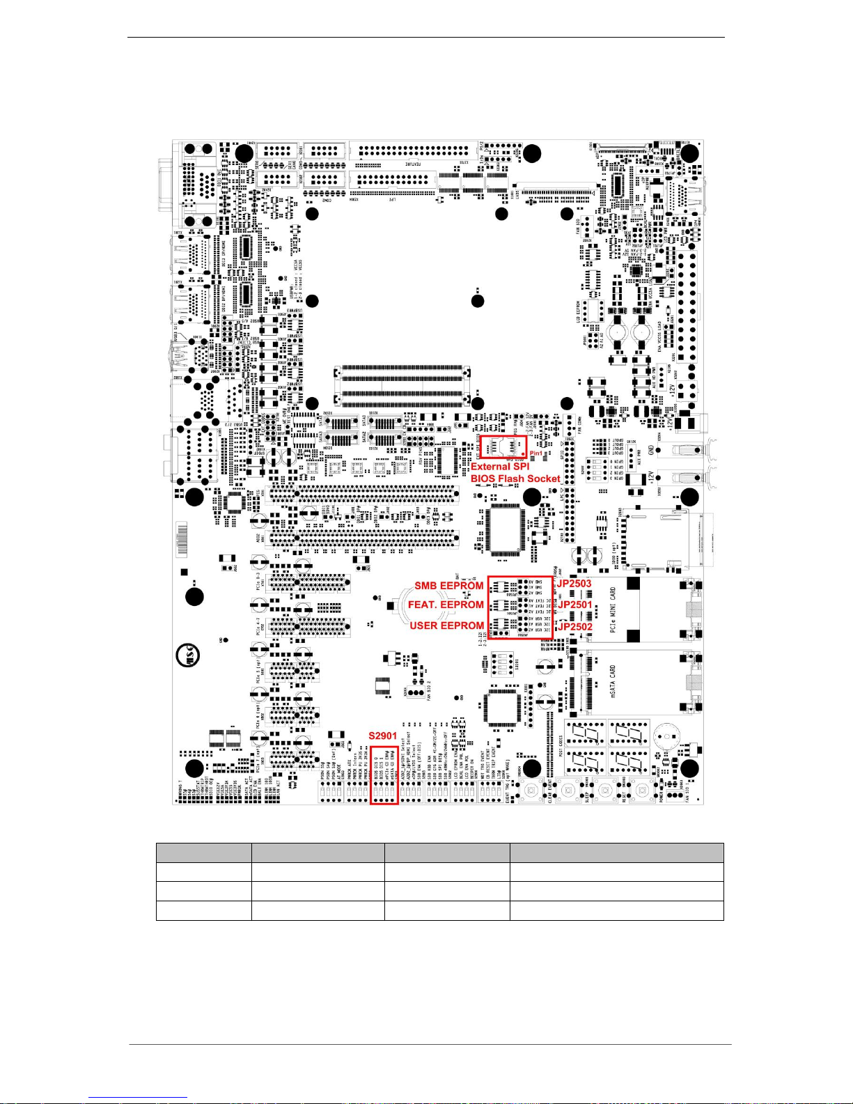
MSC C6-MB-EVA - PRELIMINARY - User Manual
53 / 63
4.25 Serial SMB EEPROM
For testing purposes a serial EEPROM (4kBit) is connected to the SMBus. To avoid address conflicts, the
address can be selected with jumpers.
JP2503
Signal name
Function
Default resistor setting
1 - 2
A0
A0 low
low
3 - 4
A1
A1 low
low
5 - 6
A2
A2 low
low
Table 38 Jumper SMB EEPROM Address
Do not use address A0 and A4. There can be an address conflict with the spd on the memory
slot.
Page 54
MSC C6-MB-EVA - PRELIMINARY - User Manual
54 / 63
4.26 Serial I2C-Bus EEPROM
For testing purposes two serial EEPROM (4kBit) are connected to the I2C bus. To avoid address
conflicts, the address can be selected with jumpers.
4.26.1 Feature I2C EEPROM
JP2501
Signal name
Function
Default resistor setting
1 - 2
A0
A0 low
high
3 - 4
A1
A1 low
high
5 - 6
A2
A2 low
high
Table 39 Jumper Feature I2C EEPROM Address
4.26.2 User I2C EEPROM
JP2502
Signal name
Function
Default resistor setting
1 - 2
A0
A0 low
high
3 - 4
A1
A1 low
high
5 - 6
A2
A2 low
high
Table 40 Jumper User I2C EEPROM Address
Note: The 10k pull up resistor at A2 is missing on rev. 3 carriers (LY30E801).
4.27 External SPI BIOS-Flash
There is a socket on the mother board, where an additional BIOS-Flash can be inserted. The
BIOS SPI flash can be selected with DIP switch S2901.
BIOS_DIS1
BIOS_DIS0
BIPOS Entry (SPI_CS#)
OFF
OFF
On module SPI (default)
OFF
ON
Carrier FWH (not supported)
ON
OFF
Carrier SPI
ON
ON
On module SPI, carrier SPI contains management data
Table 41 Jumper BIOS selection
4.28 POST-Code Display
For debugging purposes a POST code display is implemented on the base board. The display of
BIOS outputs on IO-port 80h, 84h, 90h or 94h is selected using DIP switch S3101.
SW
Port Address
1 ON
80h (Default)
1 OFF
90h
2 ON
84h (Default)
2 OFF
94h
Table 42 POST-Code Selection
4.28.1 Lattice Programming Interface
A connector used to program the PLD to decode the POST codes is implemented. To reprogram
the PLD a Lattice programming adapter is required.
Specification:
References: X3101
Connector:CAB 1001-161-008
Pin-out: Refer to Table 43
Page 55
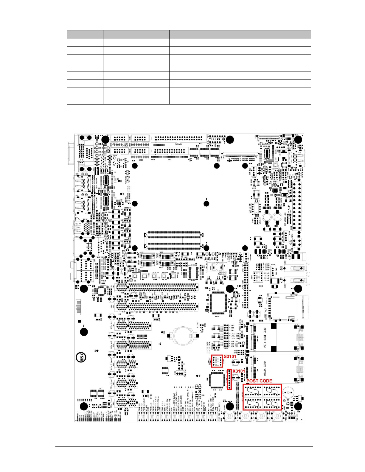
MSC C6-MB-EVA - PRELIMINARY - User Manual
55 / 63
Pin
Signal name
Function
1
VCC
Power Supply
2
SDO_TDO
Serial Data Out
3
SDI_TDI
Serial Data In
4
ISPEN#
Programming Enable
5
KEY
Key-pin
6
MODE_TMS
Programming Mode
7
GND
Ground
8
SCLK_TCK
Serial Clock
Table 43 Pin-out Lattice Programming Interface
Page 56
MSC C6-MB-EVA - PRELIMINARY - User Manual
56 / 63
4.29 Feature Connector
Many COMExpress signals are not used on this carrier. These signals and some other signals
and power planes are available at the Feature connector.
Specification Feature connector:
References: X2701
Connector:40 pin IDC-M
Pin-out: Refer to Table 44
Location: Refer to Illustration 4 Miscellaneous Parts
Pin
Signal
Pin
Signal
1
VCC5S (5V switched)
2
VCC3V3S (3,3V switched)
3
VCC5A (5V always on)
4
SATA_LED# (incl. 330R serial)
5
I2C_DAT
6
SMB_CLK
7
I2C_CLK
8
SMB_DAT
9
VCC3V3A (always on)
10
LPC_SERIRQ
11
TPM_PP (TPM presence)
12
VCC5S (5V switched)
13
SLP_S5#
14
BEEPER
15
SLP_S3#
16
SER0_TXD
17
SLP_S4#
18
SER0_RXD
19
PS_ON#
20
SMB_ALERT#
21
WAKE1#
22
CAN0_SER1_TXD
23
SUS_STAT#
24
THRM#
25
GND
26
CAN0_SER1_RXD
27
WDT (Watch dog trigger)
28
SLEEP#
29
GND
30
THRMTRIP#
31
BATLOW#
32
PCIE_WAKE#
33
GND
34
EVENT_EDGE
35
LID#
36
RESET#
37
GND
38
GND
39
PWRBTN#
40
PWR_OK
Table 44 Pin-out Feature connector
4.30 Power Supply ATX Connector
An ATX connector with additional ATX12V connector is available to power the system.
Specification ATX connector:
References: X3201
Connector:Molex 44206-0007
Pin-out: Refer to ATX specification V2.2 [2]
Specification ATX12V connector:
References: X3202
Connector:Molex 39-29-9042
Pin-out: Refer to ATX specification V2.2 [2]
Specification 2 pol. Power jack connector:
References: X3205
Connector:Kycon KLD(X)-0202-B (6.3mm, 2.5mm)
Pin-out: Refer Refer to Table 45 GND pin2 --(●-- pin1 +12V
Page 57
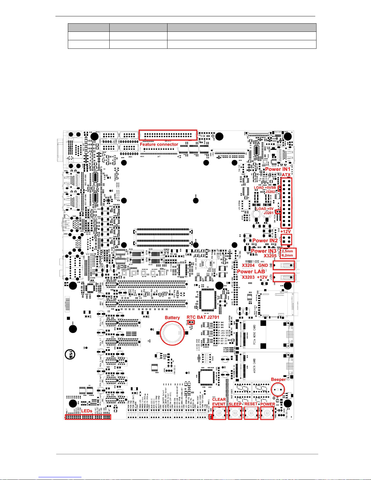
MSC C6-MB-EVA - PRELIMINARY - User Manual
57 / 63
Pin
Signal name
Function
1
+12V
VCC (inner pin 2.5mm diameter)
2
GND
Ground (shell 6.3mm diameter)
Table 45 Pin-out Power IN3 connector
4.31 Power Supply Labor Connector
The carrier can also be powered with +12VDC only.
Specification Labor connector:
References: X3203, X3204 (Power LAB)
Connector:Hirschmann PB4, 4mm, 60V, 16A.
Pin-out: Red: +12V / Black: GND
Illustration 4 Miscellaneous Parts
The LOAD jumper J3201 and J3202 adds a 100mA current at 5V ATX plane and 5VSB plane. In
some causes this can help the ATX power supply unit to turn on.
Page 58

MSC C6-MB-EVA - PRELIMINARY - User Manual
58 / 63
4.32 Battery
The RTC on the COM Express module is buffered with a socketed battery on the base board.
In order to clear the CMOS memory, the battery voltage to the COM Express module can be
disconnected via nearby RTC BAT jumper J2701.
Type of battery: 2032
References: BT2701
Connector:Renata SMTU2032-1
Location: Refer to Illustration 4 Miscellaneous Parts
4.33 Beeper
A signal generator is implemented for acoustic signals. The beeper can be enabled and disabled
with DIP switch 1 at S2906.
Type: Digisound F/DGX05P
References: LS2701
Type: Digisound F/DGX05P
Location: Refer to Illustration 4 Miscellaneous Parts
4.34 Power Button
For switching the system on a power push button has been implemented.
The PWR_BTN# signal is low-active and is connected directly to the corresponding pin of the
COM Express module.
References: SW3001
Type: ITT PTS125
Location: Refer to Illustration 4 Miscellaneous Parts
4.35 Reset Button
There is a push button for resetting the system.
The RESET# signal is low-active and is connected to the SYS_RESET#- pin of the COM Express
module.
References: SW3002
Type: ITT PTS125
Location: Refer to Illustration 4 Miscellaneous Parts
4.36 Sleep Button
There is a push button for setting the system into sleep state.
References: SW3003
Type: ITT PTS125
Location: Refer to Illustration 4 Miscellaneous Parts
4.37 Clear Event Button
There is a push button to reset the state of the event latch.
References: SW3004
Type: ITT PTS125
Location: Refer to Illustration 4 Miscellaneous Parts
Page 59
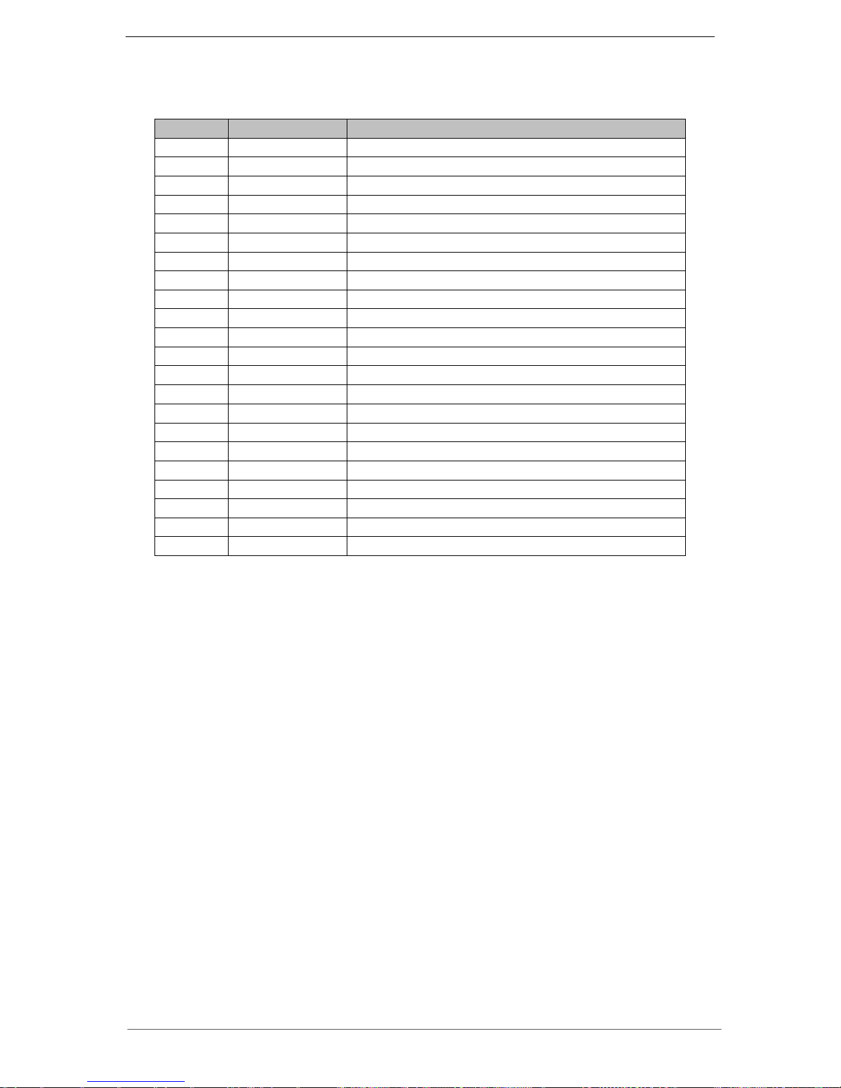
MSC C6-MB-EVA - PRELIMINARY - User Manual
59 / 63
4.38 LEDs
There are many LEDs placed on the edge of the carrier. They indicate power and system states.
Location: Refer to Illustration 4 Miscellaneous Parts
Color
Function
Description
Red
WRONG T
No type 6 module is plugged at X301.
Red
S5#
Module is in sleep state S5
Red
S4#
Module is in sleep state S4
Red
S3#
Module is in sleep state S3
Red
SUSSTAT
Module is in suspend state
Red
THRMTRIP
CPU has entered thermal shutdown.
Red
THRMTHROT
Over-temp situation has occurred.
Red
SDIO OC#
Over-current at SD Card slot.
Green
VCC12V
12V power supply ok.
Green
VCC5A
5V suspend power ok.
Green
VCC3V3A
3V3 suspend power ok.
Green
VCC5S
5V power supply ok.
Green
VCC3V3S
3V3 power supply ok.
Green
PWROK
PWR_OK signal is applied.
Yellow
SATA ACT
Indicates SATA activity.
Yellow
mSATA ACT
Indicates mSATA activity.
Green
LCD ENA
Display power is switched on.
Green
BKLT ENA
Backlight power is switched on.
Green
LINK 100
Indicates LAN 100Mps activity.
Yellow
LINK 1000
Indicates LAN 100Mps activity.
Green
LINK
Indicates LAN link.
Green
LAN ACT
Indicates LAN activity.
Table 46 LEDs Overview
4.39 WLAN LEDs
There are three yellow LEDs placed near PCIe Mini Card slot. They indicate the card type.
Wireless Wide Area Network (WWAN).
Wireless Local Area Network (WLAN).
Wireless Personal Area Network (WPAN).
Page 60
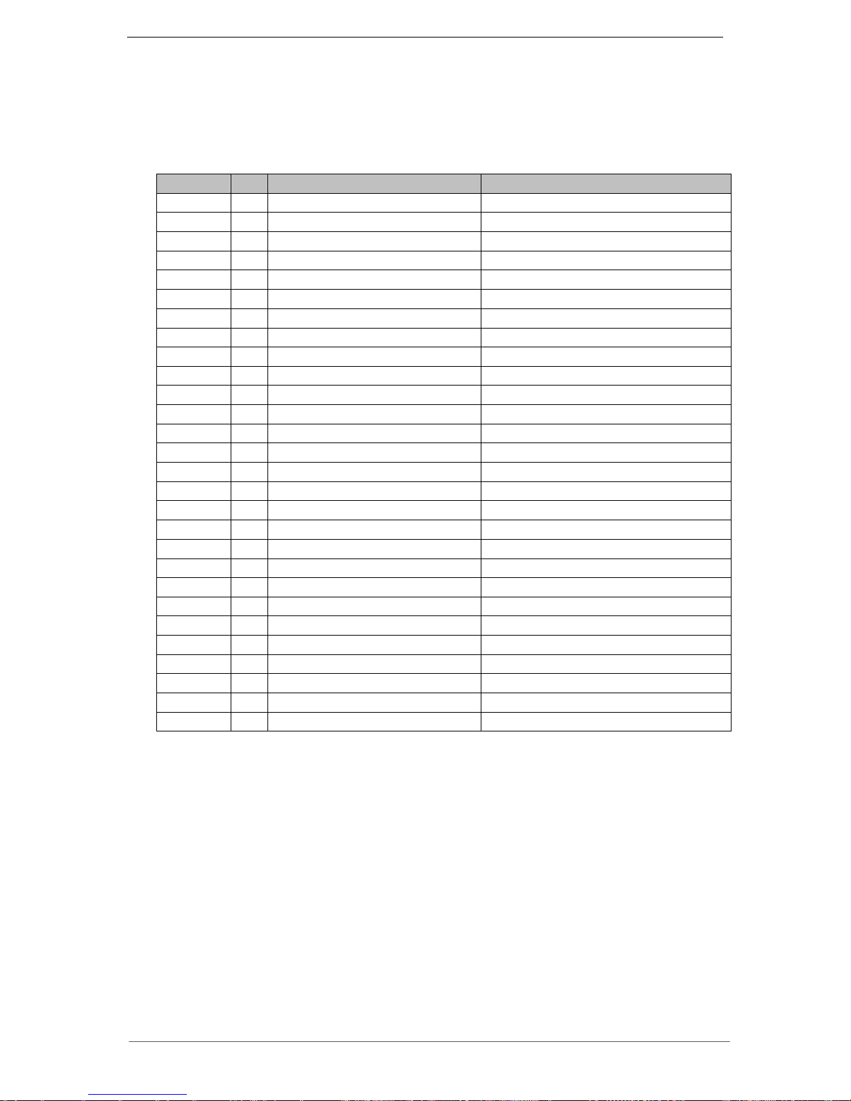
MSC C6-MB-EVA - PRELIMINARY - User Manual
60 / 63
4.40 DIP Switches
There is an array of DIP switches at the card edge to configure various functions.
References: S2901, S2902, S2903, S2904, S2905, S2906, S2908.
Type: 4pol
Location: Card edge
Reference
No.
Function
Description
S2903
4
PSON S5#
Selects source for PSON signal.
S2903
3
PSON S4#
Selects source for PSON signal.
S2903
2
PSON S3# (default on)
Selects source for PSON signal.
S2903
1
AT MODE
ATX always on (PSON is set to GND)
S2904
4
PWROK ATX (default on)
PWROK from ATX supply
S2904
3
PWROK Intern
PWROK from DC/DC (12V only mode)
S2904
2
PWROK PU 3V3S
PU 1k2 to 3V3
S2904
1
PWROK PU 3V3A
PU 1k2 to 3V3 SUS
S2901
4
BIOS DIS 0 (default off)
BIOS selection table at chapter 4.27
S2901
3
BIOS DIS 1 (default off)
BIOS selection table at chapter 4.27
S2901
2
mPCIe CD ENA#
On enables mPCIe slot (chap. 4.5)
S2901
1
mSATA CD ENA#
On enables mSATA slot (chap. 4.17)
S2905
4
ADD2_1#/SDVI Select
DDI selection
S2905
3
ADD2_2#/DP_HDMI Select
DDI selection
S2905
2
eDP#/LVDS Select
eDP / LVDS selection
S2905
1
SIO ENA / OFF = DIS
On enables SIO W83627
S2902
4
SIO KBD ENA
SIO keyboard controller enable (on)
S2902
3
SIO CFG ADR 4E=ON/2E=OFF
SIO address selection (default off, 2E)
S2902
2
SIO SPI DIS#
SIO PNP, disables SPI (default off)
S2902
1
SIO 48MHz=ON/24MHz=OFF
SIO PEN48 (default on, 48MHz)
S2906
4
LCD EPROM ENA (default on)
Off enables carrier EDID EEPROM
S2906
3
BCKL ENA POL
Backlight polarity, off = low active
S2906
2
LCD ENA POL
LVDS enable polarity, off = low active
S2906
1
BEEPER ON
On enables beeper
S2908
4
WDT TRG EVENT
Source for trigger event edge
S2908
3
CB RESET EVENT
Source for trigger event edge
S2908
2
THRM TRIP EVENT
Source for trigger event edge
S2908
1
LID#
On = 680R to GND
Table 47 DIP Switch Overview
4.41 Miscellaneous
4.41.1 Resistors for current measuring
Resistors are inserted into the power supply lines of the COM Express module, the PCI express
graphics slot as well as into every PCI slot and one PCI express x1 slot. These can be used for
current measurement.
In addition to there is one jumper to measure the current using an external wire loop and clamp
meter.
4.41.2 Ground Pins
There are several ground pins spread over the base board for connection of measurement
equipment.
Page 61
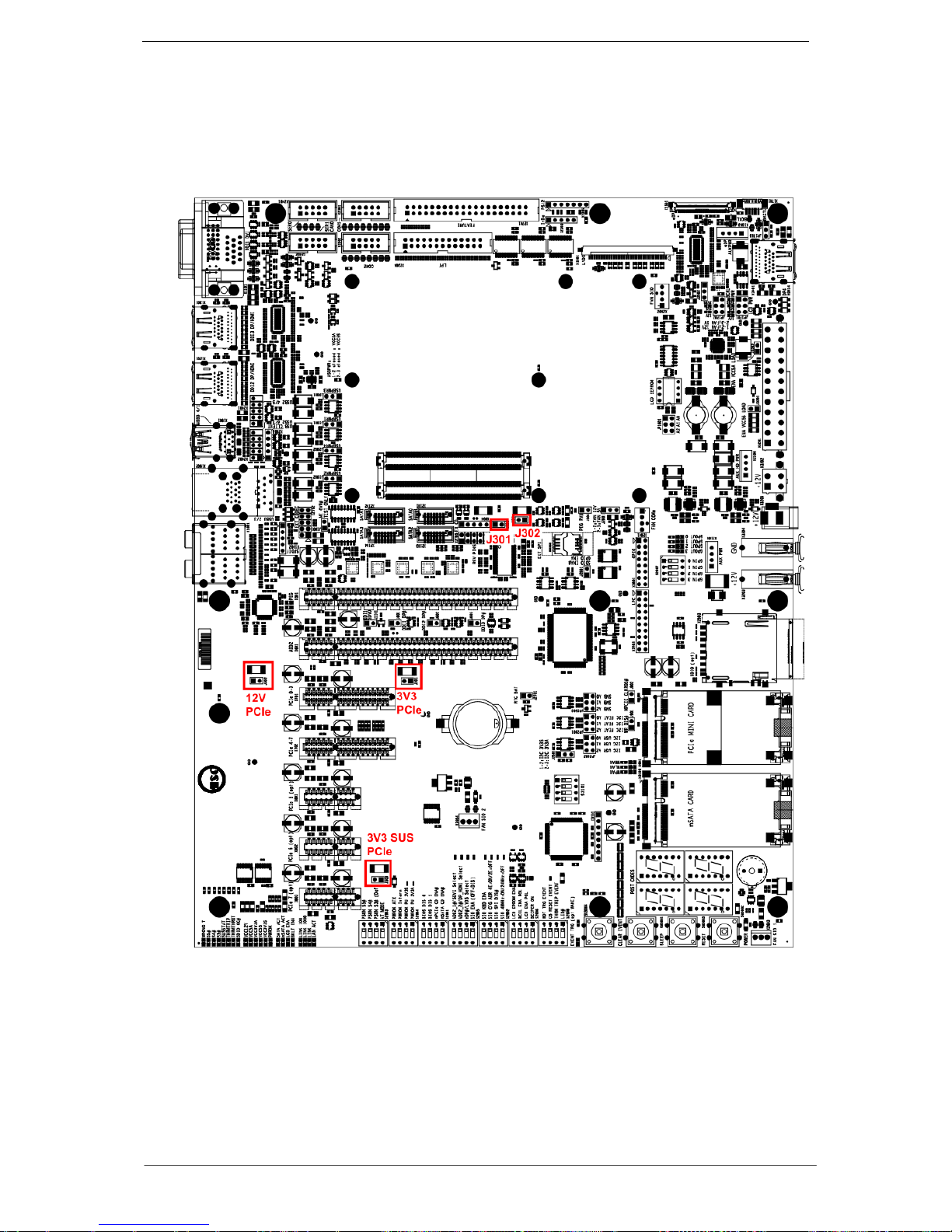
MSC C6-MB-EVA - PRELIMINARY - User Manual
61 / 63
4.41.3 Power supply current measuring
Since the sense resistors in the power supply lines of the COM Express module are removed in
rev.3, the two jumpers J301 and J302 must be set for full ATX function.
J301 can be used for +12V module current measurement.
J302 can be used for +5V Suspend module current measurement.
Illustration 5 Current Measurement
Page 62
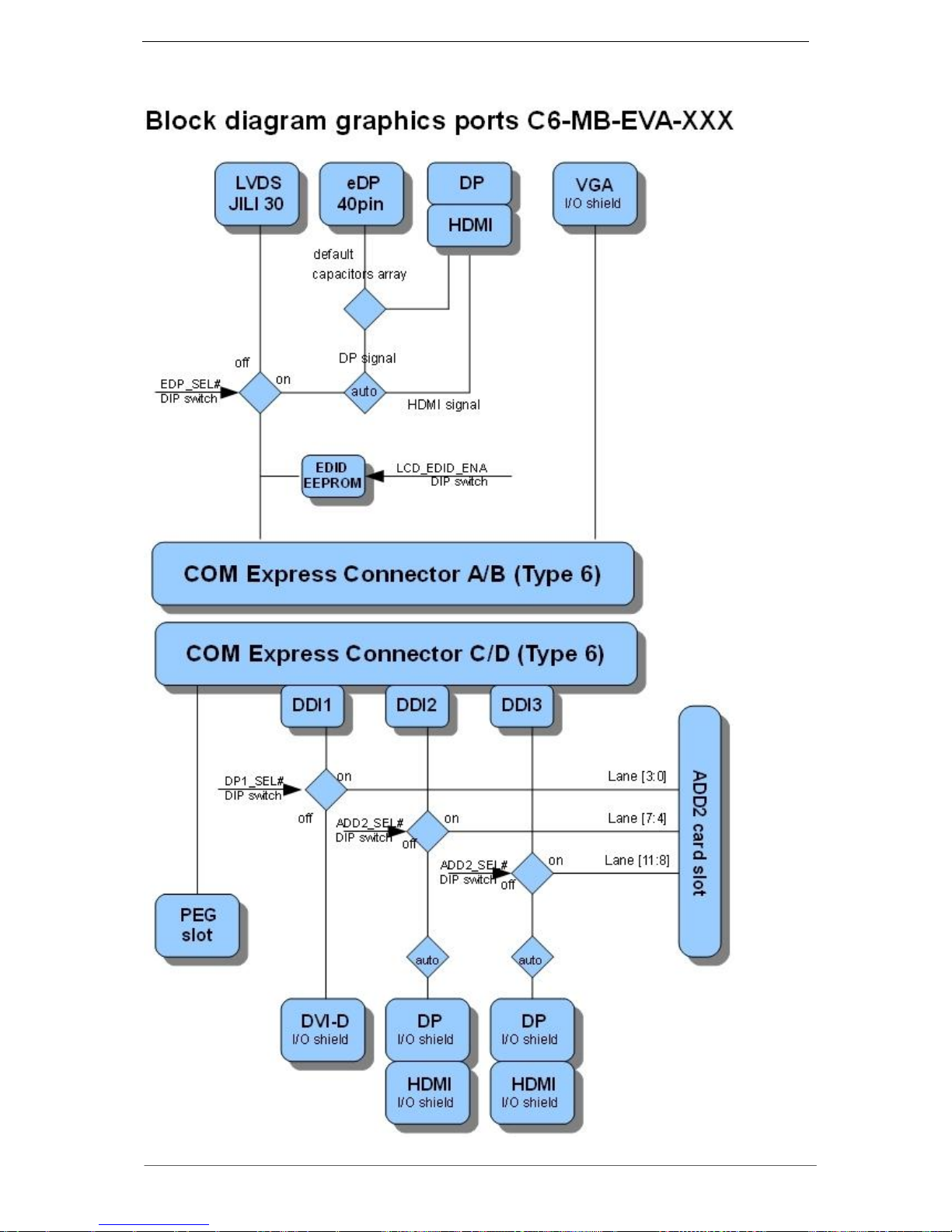
MSC C6-MB-EVA - PRELIMINARY - User Manual
62 / 63
4.42 Graphic Port Selection
Illustration 6 Block Diagram Graphics Ports
Page 63
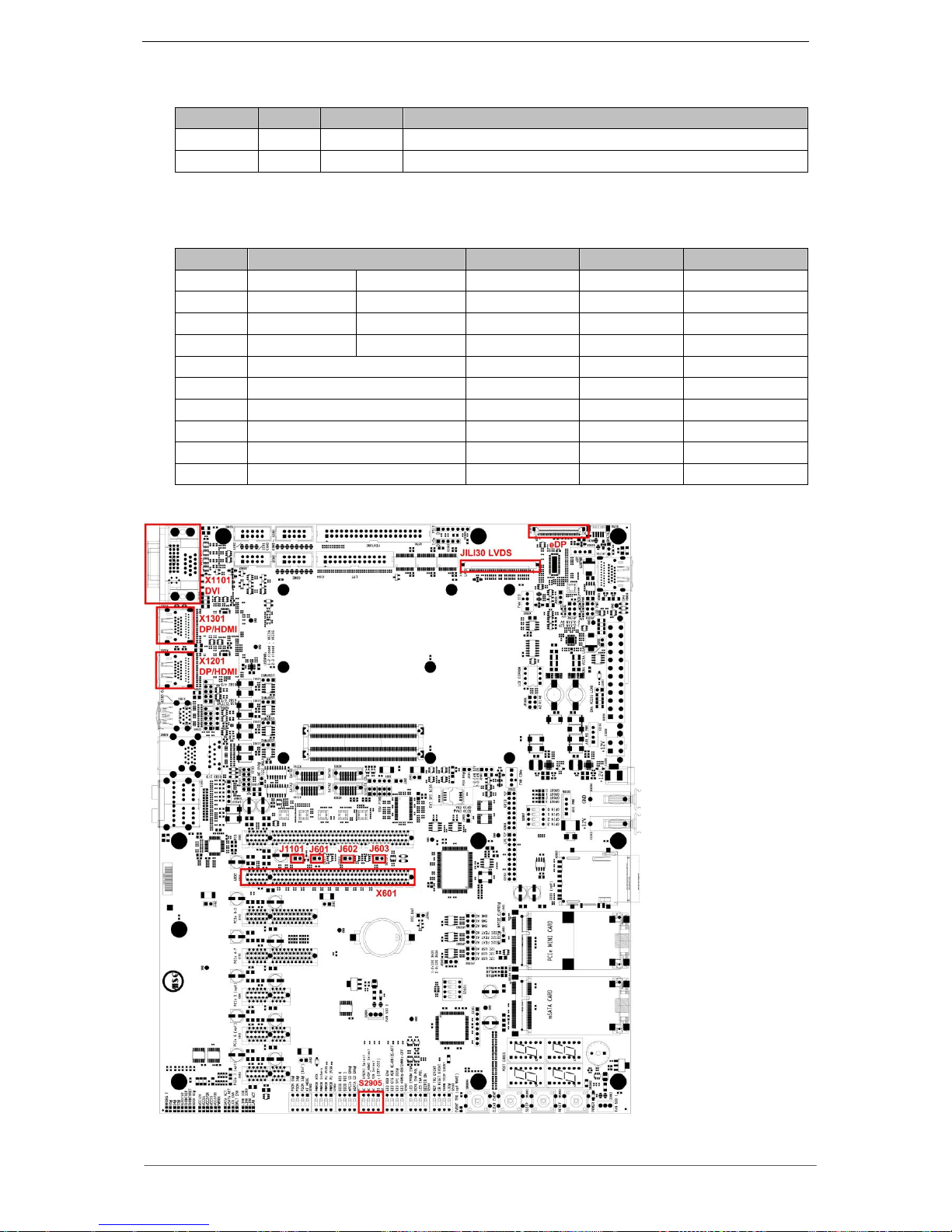
MSC C6-MB-EVA - PRELIMINARY - User Manual
63 / 63
4.42.1 JILI30 / eDP Selection
DIP Switch
No.
Status
Function
S2905
2
OFF
JILI30 (LVDS)
S2905
2
ON
eDP (embedded Display Port 40pin)
Table 48 JILI30 / eDP Selection
4.42.2 DDI Port Selection
Source
Jumper settings
DP jumper
Connector
Interface
DDI1
S2905 /4 OFF
J1101 don’t care
J601 open
X1101
DVI
DDI1
S2905 /4 ON
J1101 closed
J601 open
X601 (ADD2)
DVI / HDMI
DDI1
S2905 /4 ON
J1101 closed
J601 closed
X601 (ADD2)
DP
DDI1
S2905 /4 ON
J1101 open
J601 open
X601 (ADD2)
SDVO
DDI2
S2905 /3 OFF
J602 open
X1201
HDMI/ DP
DDI2
S2905 /3 OFF
J602 closed
X601 (ADD2)
DP
DDI2
S2905 /3 ON
J602 open
X601 (ADD2)
DVI / HDMI
DDI3
S2905 /3 OFF
J603 open
X1301
HDMI/ DP
DDI3
S2905 /3 OFF
J603 closed
X601 (ADD2)
DP
DDI3
S2905 /3 ON
J603 open
X601 (ADD2)
DVI / HDMI
Table 49 DDI Port Selection
 Loading...