

Page 1
PLATINUM
M
M
IGNATURE
F
24 BIT D
OUR
Q
UADRANT
ISCRETE
L
ADDER
3 MH
S
BY MSB TECHNOLOGY
MP-ACD311
Features
• Designed specifically for high resolution digital audio
• True voltage output, no I/V converter required
• Low unbuffered output impedance 500 Ohms
• Built in high speed buffer (MP-ACD311B only)
• Ultra high dynamic range, 135 dB typical (<130dB guaranteed)
• 0Hz to 3.125MHz conversion rate (16x oversampling @ 192kHz or 8x @ 384 kHz)
• Integrated metal shield
• Low external parts count
• Custom grades and features available
Description
Z
DAC
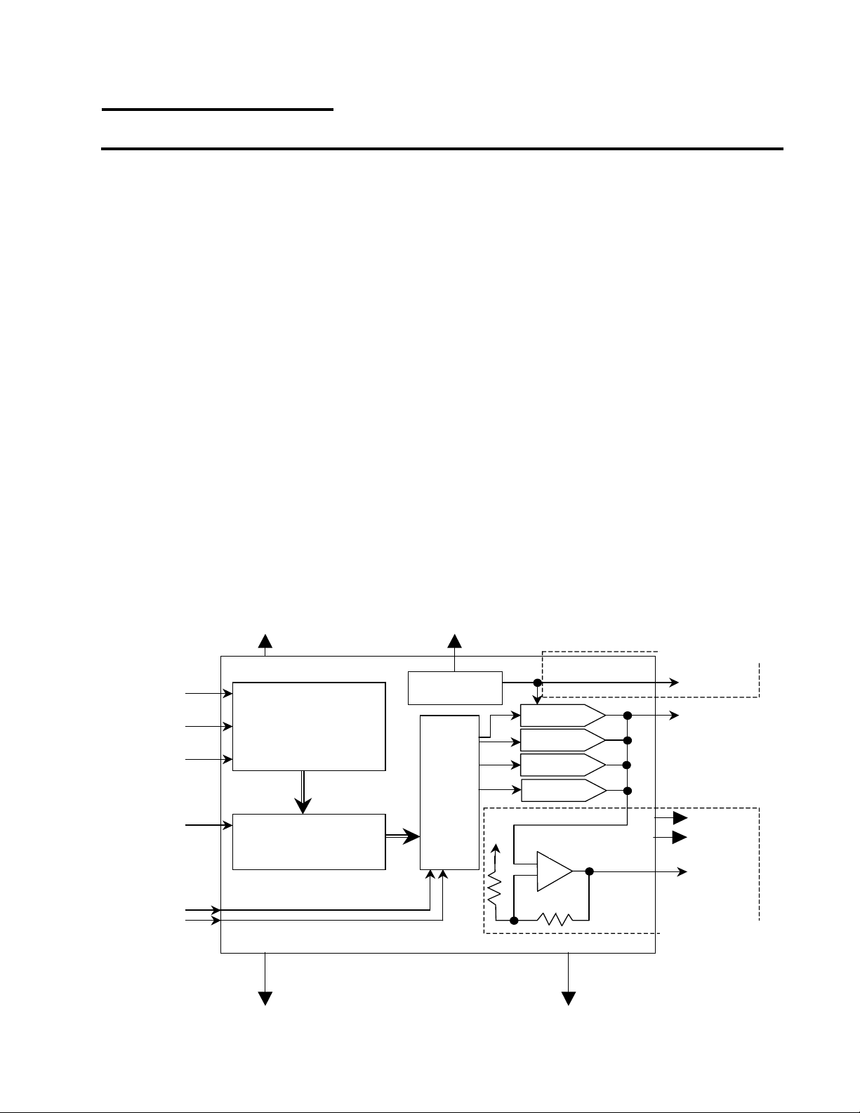
The MP-ACD311 is an ultra high performance 24 bit direct conversion audio DAC that provides unparalleled performance. The four-quadrant DAC architecture ensures the best possible performance for small and large signals without averaging (like a Delta-sigma data converter.) A fast conversion rate, low noise and distortion at all signal levels delivers the finest digital audio possible with a
minimum of external components.
Offered with an internal buffer (MP-ACD311B) or without (MP-ACD311U.)
Bit Clock
Word Clock
DATA
Reset
Differential
Conversion
Clock
+5V Digital +12V Analog
24 Bit Shift
Register
Decoding
Reference
Conversion Registers
++ DAC
+ DAC
- DAC
-- DAC
Ref
Bffr
P-ACD311U
Reference
Output
Un-buffered
Output
+ 15V
- 15V
Buffered
Output
P-ACD311B
Digital GND
2003 MSB Technology Corporation Page 1
www.MSBTECH.com 14251 Pescadero Road, La Honda, Ca 94020 Phone 650-747-0400 Fax 650-747-0405
Analog GND
Page 2

PLATINUM
IGNATURE
F
24 BIT D
OUR
Q
UADRANT
ISCRETE
L
ADDER
3 MH
DAC
S
BY MSB TECHNOLOGY
MP-ACD311
Specifications for MP-ACD311
All Specifications measured at 25ºC, +VD = 5V, +VR = 12V, +VA = 12V, -VA = -12V, FS = 384Khz, Data = 24bit
Parameter Conditions Minimum Typical Maximum Units
Resolution
Data Format
Audio Data Format 24-Bit, MSB First, Two’s Complement
Sampling Frequency 0 3125 KHz
Serial Clock Frequency 75
Digital Input
+VD = 5V
Logic High Level 3.8 5.25 V
Logic Low Level -0.25 1.6 V
Conversion Clock
+VR > 9V
+CCLK Input Range -0.25 5.25 V
-CCLK Input Range -0.25 5.25 V
Analog Output
Output Range (14) Buffered -5 5 V
Output Range (12) Unbuffered 0 5 V
Output Current (14) Buffered -25 25 mA
Output Current (12)
Unbuffered
010mA
Output Impedance (14) Buffered 5 Ohm
Output Impedance (12)
Reference Out
Unbuffered
MP-ACD311U
4.995 5.000 5.005 V
DC Accuracy
Bipolar Zero Error (14) Buffered -5 5 mV
Bipolar Zero Error (12) Unbuffered -1 1 mV
Gain Error (14) Buffered 0.8 0.8 % FSR
Gain Error (12) Unbuffered 0.5 0.5 % FSR
Dynamic Performance
THD+N 0dB 0.004 0.006 %
THD+N -60dB 0.02 0.03 %
Dynamic Range A-weighted 130 135 dB
Signal to Noise Ratio A-weighted 140 145 dB
Low Level Linearity 1KHz –90bB -0.15 0.15 dB
Settling Time 100 150 ns
Power Requirements
Positive Digital (+VD) 4.75 5.00 5.25 V
Positive Analog (+VR) 10 12 15 V
Positive Buffer (+VA)
Negative Buffer (-VA)
MP-ACD311B
MP-ACD311B
81215V
-15 -12 -8 V
-35 -10 mA
24 Bits
MHz
500 Ohm
24 50 mA
38 44 mA
10 35 mA
Z
2003 MSB Technology Corporation Page 2
www.MSBTECH.com 14251 Pescadero Road, La Honda, Ca 94020 Phone 650-747-0400 Fax 650-747-0405
Page 3
PLATINUM
BY MSB TECHNOLOGY
S
IGNATURE
F
24 BIT D
OUR
Q
ISCRETE
UADRANT
L
ADDER
MP-ACD311
3 MH
DAC
Z
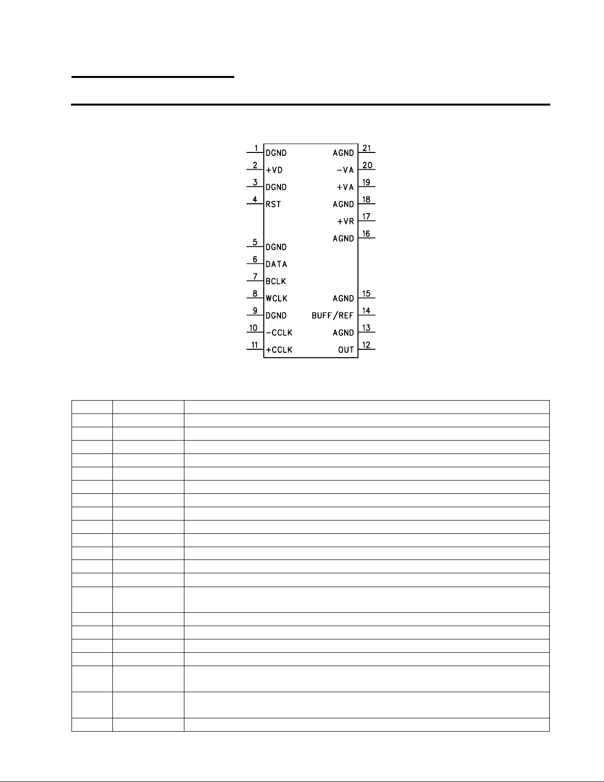
Pin Assignments for MP-ACD311
Pin Assignments are for all versions except where noted
Pin # Pin Name Function
1 DGND Digital Ground, connected internally to AGND
2 +VD Digital Power Input, 5V supply
3 DGND Digital Ground
4 RST Shift Register Reset Input, Low = Reset, High = Shift
5 DGND Digital Ground
6 DATA Two’s Compliment Data Input 24-Bit, MSB First, Right Justified
7 BCLK Bit Clock Input, Data is shifted on High to Low transition
8 WCLK Word Frame Clock, Data is latched on High to Low transition
9 DGND Digital Ground
10 -CCLK ½ DAC Conversion Clock Input, DAC converts on High to Low
11 +CCLK ½ DAC Conversion Clock Input, DAC converts on Low to High
12 OUT Unbuffered Analog Output, 500 Ohm, 0V - 5V
13 AGND Analog Ground, connected to DGND internally
14 BUFF/REF MP-ACD311B = Buffered Analog Output
MP-ACD311U = 5V Reference Output
15 AGND Analog Ground
16 AGND Analog Ground
17 +VR Internal Reference Power Supply Input, 10V - 15V
18 AGND Analog Ground
19 +VA MP-ACD311B, Buffer Power Supply Input, 8V - 15V
MP-ACD311U,NoConnection
20 -VA MP-ACD311B, Buffer Power Supply Input, -8V - -15V
MP-ACD311U,NoConnection
21 AGND Analog Ground
2003 MSB Technology Corporation Page 3
www.MSBTECH.com 14251 Pescadero Road, La Honda, Ca 94020 Phone 650-747-0400 Fax 650-747-0405
Page 4
PLATINUM
m
S
3
g
y
6
Printed by: SpectraLAB - FFT Spectral Analysis Syste
m
Licensed to: DJ
S
Fri Nov 07 12:29:27 200
3
Sampling: 48000 Hz
FFT size: 262144
Averaging: 10
Window: Hannin
g
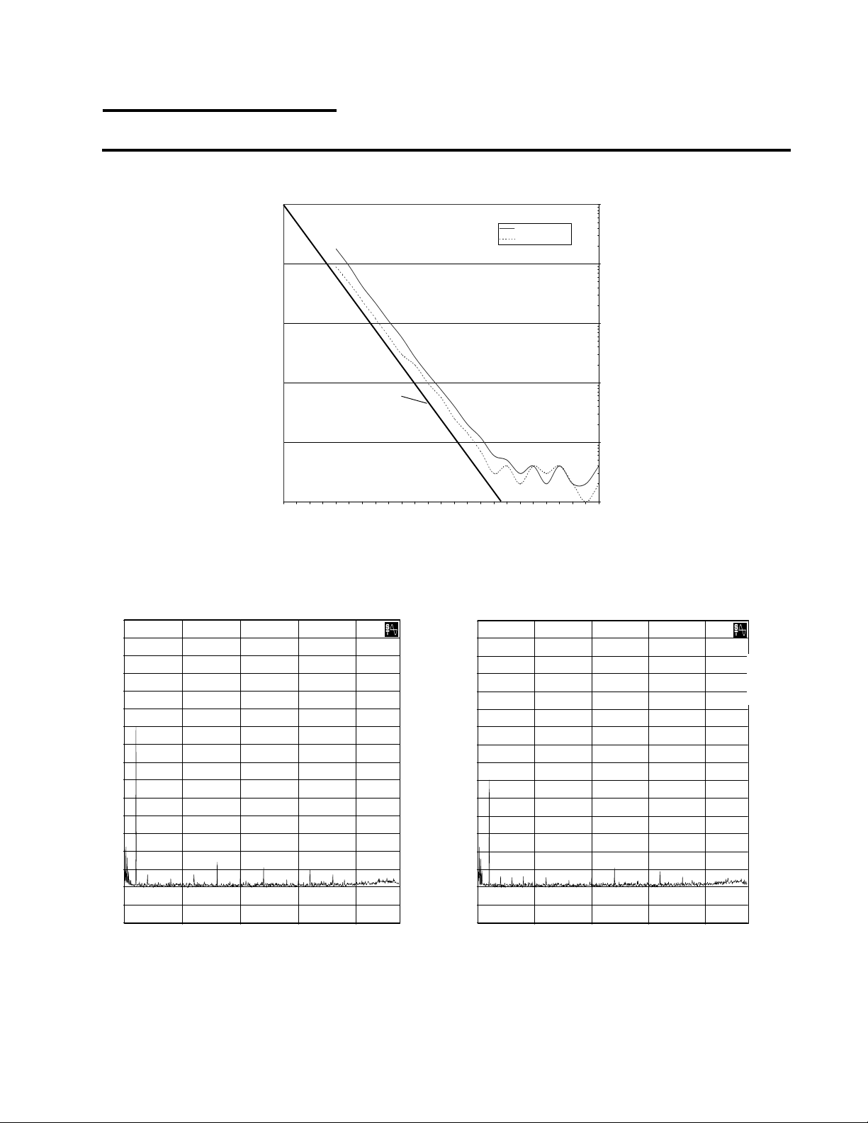
-90dB Dynaminc Range
Left Channel
dBV rms
0.0
-10.0
-20.0
-30.0
-40.0
-50.0
-60.0
-70.0
-80.0
-90.0
100.0
110.0
120.0
130.0
140.0
150.0
160.0
170.0
5.0k 10.0k 15.0k 20.0k
Frequenc
y
(Hz)
Peak: -89.
6
BY MSB TECHNOLOGY
S
IGNATURE
F
24 BIT D
OUR
Q
Typical DAC
Typical Ballanced DAC
ISCRETE
UADRANT
L
ADDER
MP-ACD311
100
10
1
3 MH
DAC
Z
Sampling: 48000 Hz
FFT size: 262144
Averaging: 10
Window: Hannin
0.0
-10.0
-20.0
-30.0
-40.0
-50.0
-60.0
-70.0
-80.0
-90.0
dBV rms
100.0
110.0
120.0
130.0
140.0
150.0
160.0
170.0
- 60 dB Dynamic Range FFT -90 dB Dynamic Range FFT
5.0k 10.0k 15.0k 20.0k
2003 MSB Technology Corporation Page 4
www.MSBTECH.com 14251 Pescadero Road, La Honda, Ca 94020 Phone 650-747-0400 Fax 650-747-0405
-60dB Dynaminc Range
Left Channel
Frequenc
(Hz)
24 bit theoretical limit
Signal Level (dB)
Printed by: SpectraLAB - FFT Spectral Analysis Syste
Licensed to: DJ
Fri Nov 07 12:30:49 200
Peak: -59.
0.1
THD + N (%)
0.01
0.001
0-6-12-18-24-30-36-42-48-54-60-66-72-78-84-90-96-102-108-114-120-126-132-138-144
Page 5
PLATINUM
IGNATURE
F
24 BIT D
OUR
Q
UADRANT
ISCRETE
L
ADDER
3 MH
DAC
S
BY MSB TECHNOLOGY
MP-ACD311
Data Interface
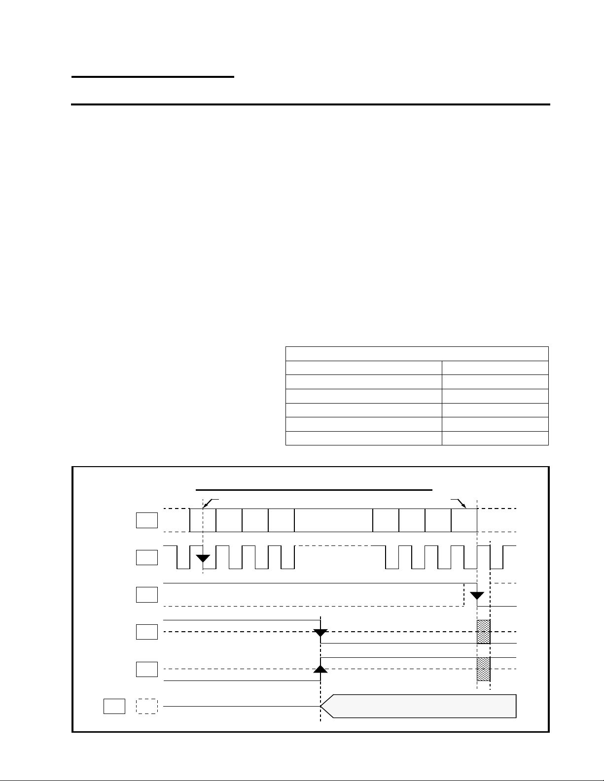
The audio data interface is designed for simple connection to most digital filters. A two’s compliment data
coding scheme was chosen for ease in digital signal inversion (only one inverter is required) and digital muting
(an all high or low data signal will produce an output within 1 LSB of Bipolar Zero.) Data is presented to the
DATA (6) pin serially. After a setup time of 3 ns (min) the falling edge of BCLK (7) shifts the data into the
internal shift register. 24 cycles or more of BCLK (7) are required per frame to shift the data into the proper
position, less than 24 cycles of BCLK (7) during one frame will cause the new data to be misaligned and a
portion of the previous data will not be cleared causing erroneous data to be presented for decoding. After the
last falling edge (5 ns min) of BCLK (7) in a frame the falling edge of WCLK (8) latches the data for decoding.
Immediately after the high to low transition of WCLK (8) internal decoding takes place, during the 20ns after
the high to low transition of WCLK (8) the data presented to the DAC is in an indeterminate state. If a conversion
(a high to low transition of –CCLK (10)) is initiated during this interval an erroneous output will occur.
To combat conversion period instability (jitter) a separate differential clock (CCLK) input is provided for
conversion. CCLK may transition asynchronously from all other signals provided that it does not initiate a
conversion within the 20ns after a high to low transition of WCLK (8). CCLK is the input of an ultra high-speed
comparator allowing compatibility with CMOS, TTL, LVCMOS, PECL or LVDS clock signals. Non-differential
signals will require a threshold to be set for the
unused input, a divider between ground and
power with a bypass capacitor is recommended.
Reset RST (4) asynchronously clears the
contents of the shift register to zero, this is
presented for decoding on the next falling
WCLK (8) and present at the DACs output on
the following conversion clock.
100000000000000000000000 Positive Full Scale
111111111111111111111110 Zero +2LSB
111111111111111111111111 Zero +1LSB
000000000000000000000000 Bipolar Zero
000000000000000000000001 Zero –1LSB
011111111111111111111111 Negative Full Scale
Two’s Compliment Coding
Z
Digital Interface Timing
MSB LSB
B2
DATA
BCLK
WCLK
-CCLK
+CCLK
12
2003 MSB Technology Corporation Page 5
www.MSBTECH.com 14251 Pescadero Road, La Honda, Ca 94020 Phone 650-747-0400 Fax 650-747-0405
6
7
8
10
11
14
B1
B3 B4 B24B23B22B21
DAC Output
Page 6
PLATINUM
BY MSB TECHNOLOGY
PLATINUM
BY MSB TECHNOLOGY
3 MH
S
IGNATURE
Signature
24 BIT D
Z FOUR
L
ADDER
F
OUR
ISCRETE
Q
UADRANT
DAC
24 BIT D
Q
UADRANT
MP-ACD311
ISCRETE
L
ADDER
3 MH
DAC
Z
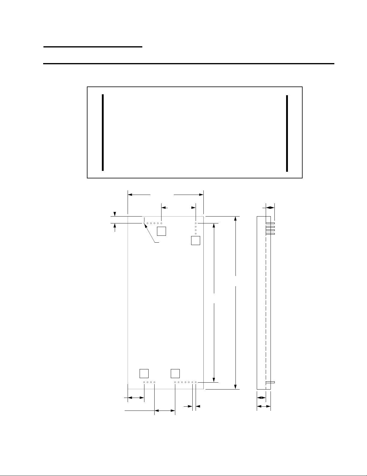
.200"
2.200"
16
Ø.035"
Top View
MP-ACD
1.000"
12
311
4.600"
.250"
5.000" ±.050
PLATINUM
Side View
BY MSB TECHNOLOGY
15
.475" ±.050
.600"
.100"
.260"
.400"
MSB Technology DAC Module
2003 MSB Technology Corporation Page 6
www.MSBTECH.com 14251 Pescadero Road, La Honda, Ca 94020 Phone 650-747-0400 Fax 650-747-0405
Page 7
PLATINUM
IGNATURE
F
24 BIT D
OUR
Q
UADRANT
ISCRETE
L
ADDER
3 MH
DAC
Z
S
BY MSB TECHNOLOGY
MP-ACD311
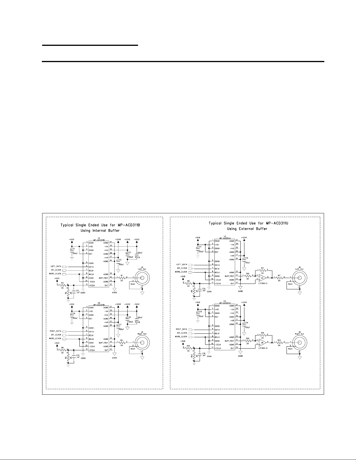
Circuit Example
The circuit below shows the typical connections for this DAC module. MSB typically
recommends a high oversampling ratio digital filter without analog filtering as shown below. An analog
reconstruction filter may be added if desired for reduced high frequency energy or for use as a nonoversampling DAC. The MP-ACD311B contains an internal buffer while the MP-ACD311U provides
a low impedance reference out for easy DC restoration without a servo.
2003 MSB Technology Corporation Page 7
www.MSBTECH.com 14251 Pescadero Road, La Honda, Ca 94020 Phone 650-747-0400 Fax 650-747-0405
 Loading...