


MPS MP86963DUT Schematic [ru]
MP86963
c
High Efficiency, 20A, 27V Intelli-Phase
(Integrated HS/LS FETs and Driver) in a 5x5mm QFN
The Future of Analog IC Technology
DESCRIPTION
The MP86963 is a monolithic Half Bridge with
built-in internal power MOSFETs and gate
driver. It achieves 20A continuous output
current over a wide input supply range.
Integrating the Driver and MOSFETs results in
high efficiency due to optimal dead time control
and parasitic inductance reduction.
The MP86963 is a Monolithic IC designed to
drive up to 20A per phase. Housed in a very
small 5x5mm TQFN Packge, this device can be
operated from 100kHz to 1MHz operation.
The IC is intended to work with 3.3V tri-state
output controllers.
The MP86963 is ideal for notebook applications
where efficiency and small size are a premium.
FEATURES
• Wide 4.5V to 21V Operating Input Range
• 20A Output Current
• Simple Logic Interface (3.3V)
• Operate from 100kHz to 1MHz
• Accepts 3-state PWM Input
• Suitable for single-/multi-phase operation
• Available in a 5mm x 5mm TQFN Package
• ROHS6 Compliant
APPLICATIONS
• Power modules
• Notebook, Core Voltage
• Graphic Card Core Regulators
All MPS parts are lead-free and adhere to the RoHS directive. For MPS green
status, please visit MPS website under Quality Assurance. “MPS” and “The
Future of Analog IC Technology” are Registered Trademarks of Monolithi
Power Systems, Inc.
This Product is Patent Pending.
TM
Solution
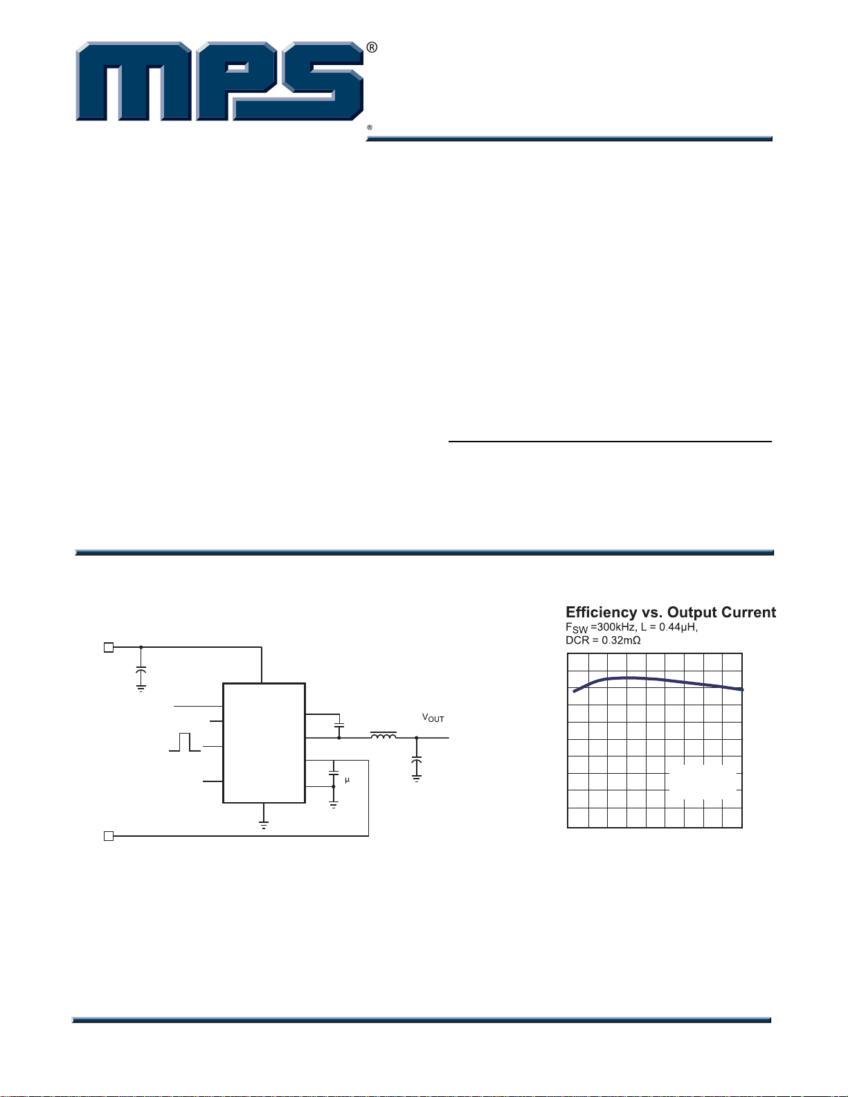
TYPICAL APPLICATION
V
IN
4.5V-21V
C
IN
ON/OFF
V
CC
5V
4
7
6
5
EN
VCC IO
PWM
MP86963
SYNC
IN
AGND
9
BST
VCC
GND
3
SW
8
100nF
2
10-18
C6
100
95
90
85
L
Cs
1
F
0.8V to 1.2V @ 20A
C
OUT
80
75
70
65
EFFICIENCY (%)
60
55
50
2 4 6 8 10 12 14 16 18 20
OUTPUT CURRENT (A)
VIN=12V
=1.2V
V
OUT
MP86963 Rev.1.22 www.MonolithicPower.com 1
12/26/2013 MPS Proprietary Information. Patent Protected. Unauthorized Photocopy and Duplication Prohibited.
© 2013 MPS. All Rights Reserved.
MP86963 –20A, 27V INTELLI-PHASE
TM
SOLUTION INTEGRATED HS/LS FETS AND DRIVER IN A 5X5mm QFN
ORDERING INFORMATION
Part Number* Package Top Marking Free Air Temperature(TA)
MP86963DUT 5x5 TQFN 86963UT
* For Tape & Reel, add suffix –Z (e.g. MP86963DUT–Z);
For RoHS compliant packaging, add suffix –LF (e.g. MP86963DUT–LF–Z)
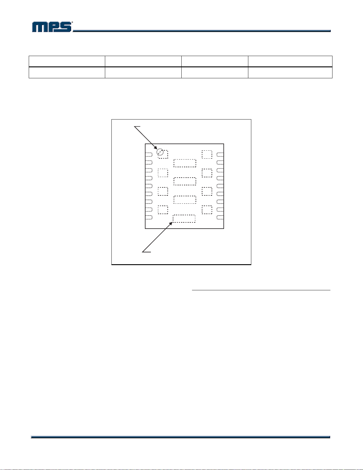
PACKAGE REFERENCE
PIN 1 ID
N/C
VCC
AGND
EN
SYNC
PWM
VCC IO
BST
1
IN
2
3
IN
4
5
IN
6
7
8
IN
9
IN
SW
SW
SW
SW
GND
GND
GND
GND
18
GND
17
GND
16
GND
15
GND
14
GND
13
GND
12
GND
11
GND
10
GND
-40°C to +85°C
EXPOSED PAD
CONNECT TO PIN
ABSOLUTE MAXIMUM RATINGS
(1)
Supply Voltage VIN....................................... 27V
V
(DC) .................................-0.3V to VIN +0.3V
SW
V
(20ns) ....................................-3V to VIN +3V
SW
V
...................................................... VSW + 6V
BST
All Other Pins..................................-0.3V to +6V
Continuous Power Dissipation (T
= +25°C)
A
(2)
............................................................. 3.8W
Junction Temperature...............................150°C
Lead Temperature ....................................260°C
Storage Temperature............... -65°C to +150°C
Recommended Operating Conditions
(3)
Supply Voltage VIN...........................4.5V to 21V
V
Driver Voltage………………….4.5V to 5.5V
CC
Operating Junct. Temp (T
)...... -40°C to +125°C
J
Thermal Resistance
(4)
θ
JA
θJC
5x5 TQFN ...............................33 ....... 8.... °C/W
Notes:
1) Exceeding these ratings may damage the device.
2) The maximum allowable power dissipation is a function of the
maximum junction temperature T
ambient thermal resistance θ
. The maximum allowable continuous power dissipation at
T
A
any ambient temperature is calculated by P
)/ θJA. Exceeding the maximum allowable power dissipation
T
A
will cause excessive die temperature.
3) The device is not guaranteed to function outside of its
operating conditions.
4) Measured on JESD51-7, 4-layer PCB.
(MAX), the junction-to-
J
, and the ambient temperature
JA
(MAX)=(TJ(MAX)-
D
MP86963 Rev.1.22 www.MonolithicPower.com 2
12/26/2013 MPS Proprietary Information. Patent Protected. Unauthorized Photocopy and Duplication Prohibited.
© 2013 MPS. All Rights Reserved.
MP86963 –20A, 27V INTELLI-PHASE
TM
SOLUTION INTEGRATED HS/LS FETS AND DRIVER IN A 5X5mm QFN
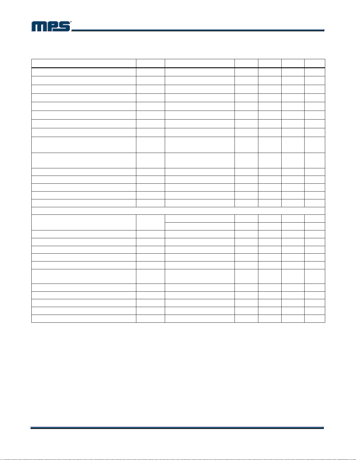
ELECTRICAL CHARACTERISTICS
VIN = 12V, TA = +25°C, unless otherwise noted.
Parameters Symbol Condition Min Typ Max Units
ICC Standby I
I
(Shutdown) I
IN
IIN Standby I
CC_StdbyVCC
VCC = 0V 1 5 μA
IN (Off)
IN_Stdby
Rise Time I
Fall Time I
Minimum On-Time 55 ns
Dead-Time Rising 5 ns
Dead-Time Falling 10 ns
V
Under Voltage Lockout Threshold
CC
Rising
VCC Under Voltage Lockout Threshold
Hysteresis
SYNC Pull-Up Current I
3.7 4.2 V
470 mV
SYNC=0V -14 μA
SYNC
SYNC Logic High Voltage 2 V
SYNC Logic Low Voltage 0.4 V
EN Input Low Voltage 0.4 V
En Input High Voltage 2 V
PWM Input
Input Current I
PWM
VCCIO 2.9 3.3 3.6 V
PWM Low to Tri-State Threshold 1.10 V
PWM Tri-State to High Threshold 2.25 V
PWM High to Tri-State Threshold 2.10 V
PWM Tri-State to Low Threshold 0.75 V
Tri-State Shutdown Holdoff Time t
UG/LG Three-State Propagation Delay t
USW Turn-Off Propagation Delay t
LSW Turn-Off Propagation Delay t
USW Turn-On Propagation Delay t
LSW Turn-On Propagation Delay t
TSSHD
20 ns
PTS
VCC=5V 40 ns
PDUL
VCC=5V 25 ns
PDLL
VCC=5V 30 ns
PDUH
VCC=5V 50 ns
PDLH
=5V, PWM=EN=LO 550 610 μA
VCC =5V, PWM=EN=LO 1 μA
= 20A 5 ns
OUT
= 20A 3 ns
OUT
V
=3.3V 370 μA
PWM
V
=0V -370 μA
PWM
V
=5V,
CC
Temperature=25°C
100 ns
MP86963 Rev.1.22 www.MonolithicPower.com 3
12/26/2013 MPS Proprietary Information. Patent Protected. Unauthorized Photocopy and Duplication Prohibited.
© 2013 MPS. All Rights Reserved.
MP86963 –20A, 27V INTELLI-PHASE
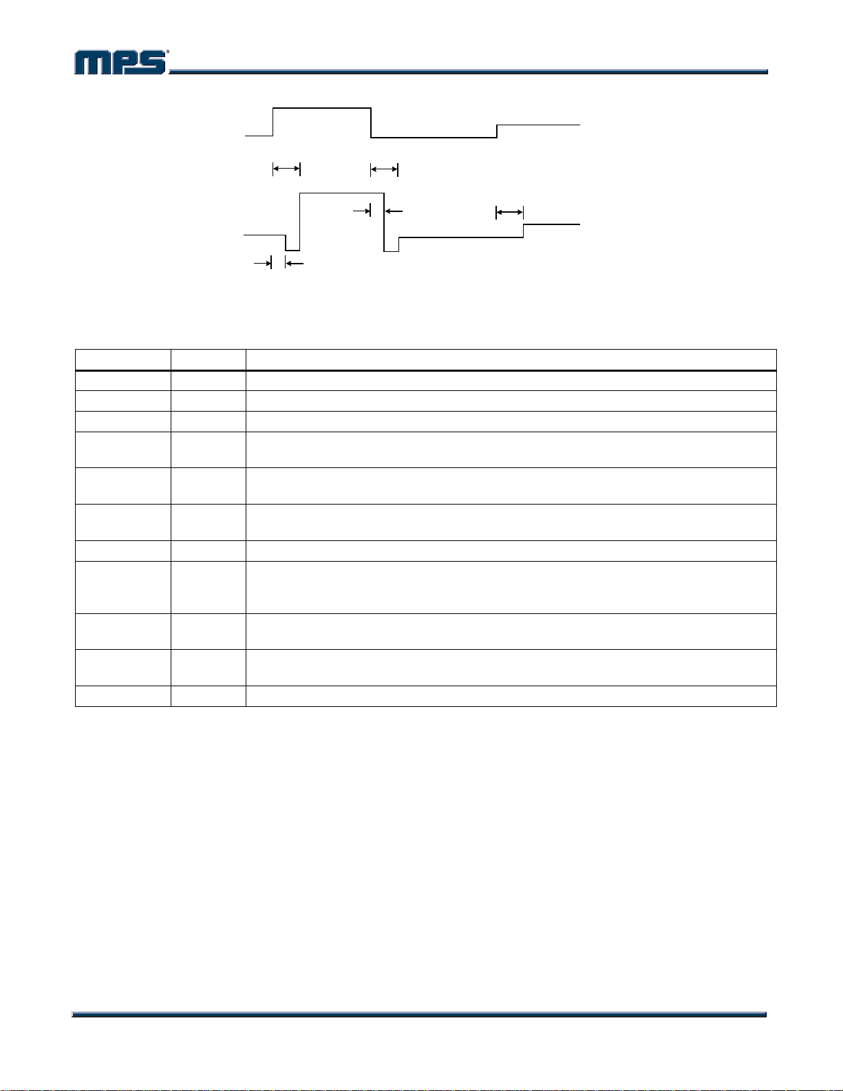
PWM
TM
SOLUTION INTEGRATED HS/LS FETS AND DRIVER IN A 5X5mm QFN
SW
0V
t
t
PDLL
PDUH
t
PDUL
t
PDLH
t
TSSHD
Figure 1—Timing Diagram
PIN FUNCTIONS
Pin # Name Description
1 NC Not Connected.
2 VCC Low-Side Driver Bias Supply. Decouple with a 1µF ceramic capacitor.
3 AGND Signal Ground.
4 EN
5 SYNC
6 PWM
7 VCC IO Reference voltage that connects to PWM driver supply.
8 BST
9
Exposed Pad
10–18
Exposed Pad
Exposed Pad SW Switch Output. These pins are fused together.
Active High On/Off Control. Pulling this Pin Low forces the SW Pin to be in a high
impedance state.
Leaving this pin Open enables theLower Synchronous Switch. Pulling it Low forces
the Lower Switch into Diode Emulation mode.
Pulse Width Modulation Control. Accepts three-state input. Force PWM to midstate or
open to place SW into high impedance state.
Bootstrap. This capacitor is needed to drive the power switch’s gate above the supply
voltage. It is connected between SW and BST pins to form a floating supply across
the power switch driver.
IN
GND Power Ground.
Supply Voltage. C
input.
is needed to prevent large voltage spikes from appearing at the
IN
V
OUT
MP86963 Rev.1.22 www.MonolithicPower.com 4
12/26/2013 MPS Proprietary Information. Patent Protected. Unauthorized Photocopy and Duplication Prohibited.
© 2013 MPS. All Rights Reserved.