

MPS MP3410 Datasheet
MP3410
1.3A, 550kHz Synchronous
Rectified Step-up Converter
The Future of Analog IC Technology
DESCRIPTION
The MP3410 is a highly efficient, synchronous,
fixed frequency, current-mode step-up converter
with output to input disconnect, inrush current
limiting and internal soft-start. It includes an error
amplifier, ramp generator, comparator, N-Channel
switch and P-Channel synchronous rectified
switch (which greatly improves efficiency). The
output disconnect feature allows the output to be
completely isolated from the input in shutdown
mode.
The 550kHz switching frequency allows for
smaller external components producing a
compact solution for a wide range of load currents.
The internal compensation and soft-start
minimizes the external component count and
limits the inrush current during startup. The
MP3410 has integrated power MOSFET which
can support up to 6V output and typical 1.3A
switch current.
The MP3410 is offered in a thin SOT23-5
package.
FEATURES
• Over 90% Efficiency
• Output to Input Disconnect at Shutdown Mode
• Internal Synchronous Rectifier
• Inrush Current Limiting and Internal Soft-Start
• Internal Compensation
• 1.3A Typical Switch Current Limit
• 550kHz Fixed Switching Frequency
• Zero Current Shutdown Mode
• Thermal Shutdown
• 5-Pin TSOT-23 Package
APPLICATIONS
• MP3 Players
• Handheld Computers and PDAs
• Digital Still and Video Cameras
• External Modems
• Small LCD Displays
For MPS green status, please visit MPS website under Quality Assurance.
“MPS” and “The Future of Analog IC Technology” are Registered Trademarks of
Monolithic Power Systems, Inc.
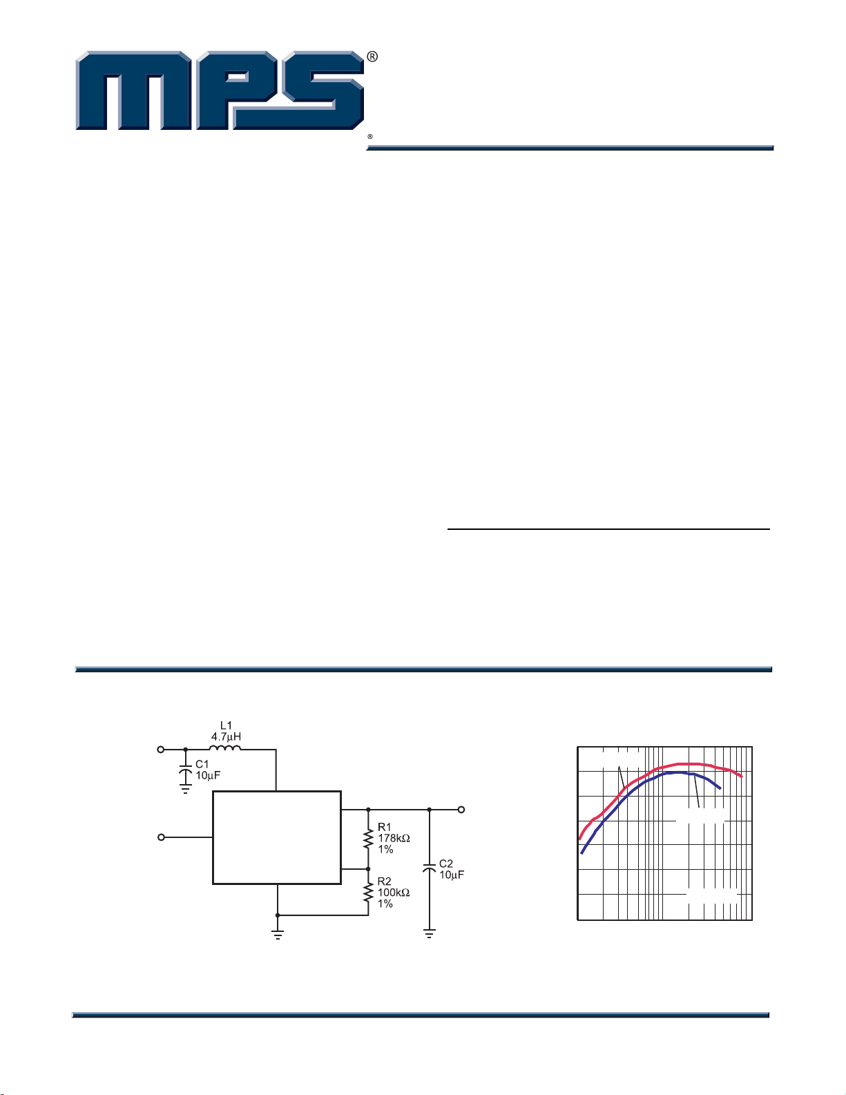
TYPICAL APPLICATION
V
IN
1.8V - 3.2V
4
SW
EN
5
EN
MP3410
GND
2
OUT
FB
Efficiency vs
Load Current
100
3
1
V
OUT
3.3V
400mA
EFFICIENCY (%)
VIN=3.6V
90
80
70
60
50
40
30
10 100 1000
LOAD CURRENT (mA)
VIN=2.4V
V
OUT
=5V
MP3410 Rev. 1.12 www.MonolithicPower.com 1
6/30/2011 MPS Proprietary Information. Patent Protected. Unauthorized Photocopy and Duplication Prohibited.
© 2011 MPS. All Rights Reserved.
MP3410 — 1.3A, 550kHz SYNCHRONOUS RECTIFIED STEP-UP CONVERTER
ORDERING INFORMATION
Part Number* Package Top Marking Free Air Temperature (TA)
MP3410DJ
TSOT23-5
P3
-40°C to +85°C
* For Tape & Reel, add suffix –Z (e.g. MP3410DJ–Z)
For RoHS compliant packaging, add suffix –LF (e.g. MP3410DJ–LF–Z)
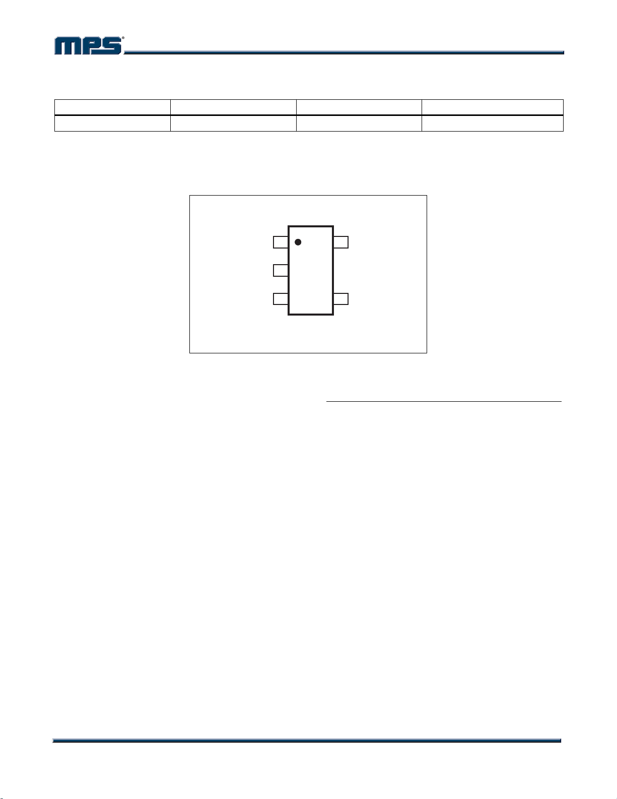
PACKAGE REFERENCE
TOP VIEW
FB
GND
OUT
1
2
3
TSOT23-5
54EN
SW
ABSOLUTE MAXIMUM RATINGS
(1)
All Pins.........................................-0.3V to +6.5V
Continuous Power Dissipation (T
= +25°C)
A
(2)
........................................................... 0.47W
Storage Temperature............... -65°C to +150°C
Recommended Operating Conditions
(3)
Supply Voltage VIN.............................1.8V to 6V
Output Voltage V
Maximum Junction Temp. (T
...........................2.5V to 6V
OUT
) .............. +125°C
J
Thermal Resistance
(4)
θ
JA
θJC
TSOT23-5.............................. 220.... 110.. °C/W
Notes:
1) Exceeding these ratings may damage the device.
2) The maximum allowable power dissipation is a function of the
maximum junction temperature T
ambient thermal resistance
. The maximum allowable continuous power dissipation at
T
A
any ambient temperature is calculated by P
)/JA. Exceeding the maximum allowable power dissipation
T
A
will cause excessive die temperature, and the regulator will go
into thermal shutdown. Internal thermal shutdown circuitry
protects the device from permanent damage.
3) The device is not guaranteed to function outside of its
operating conditions.
4) Measured on JESD51-7 4-layer board.
(MAX), the junction-to-
J
, and the ambient temperature
JA
(MAX)=(TJ(MAX)-
D
MP3410 Rev. 1.12 www.MonolithicPower.com 2
6/30/2011 MPS Proprietary Information. Patent Protected. Unauthorized Photocopy and Duplication Prohibited.
© 2011 MPS. All Rights Reserved.
MP3410 — 1.3A, 550kHz SYNCHRONOUS RECTIFIED STEP-UP CONVERTER
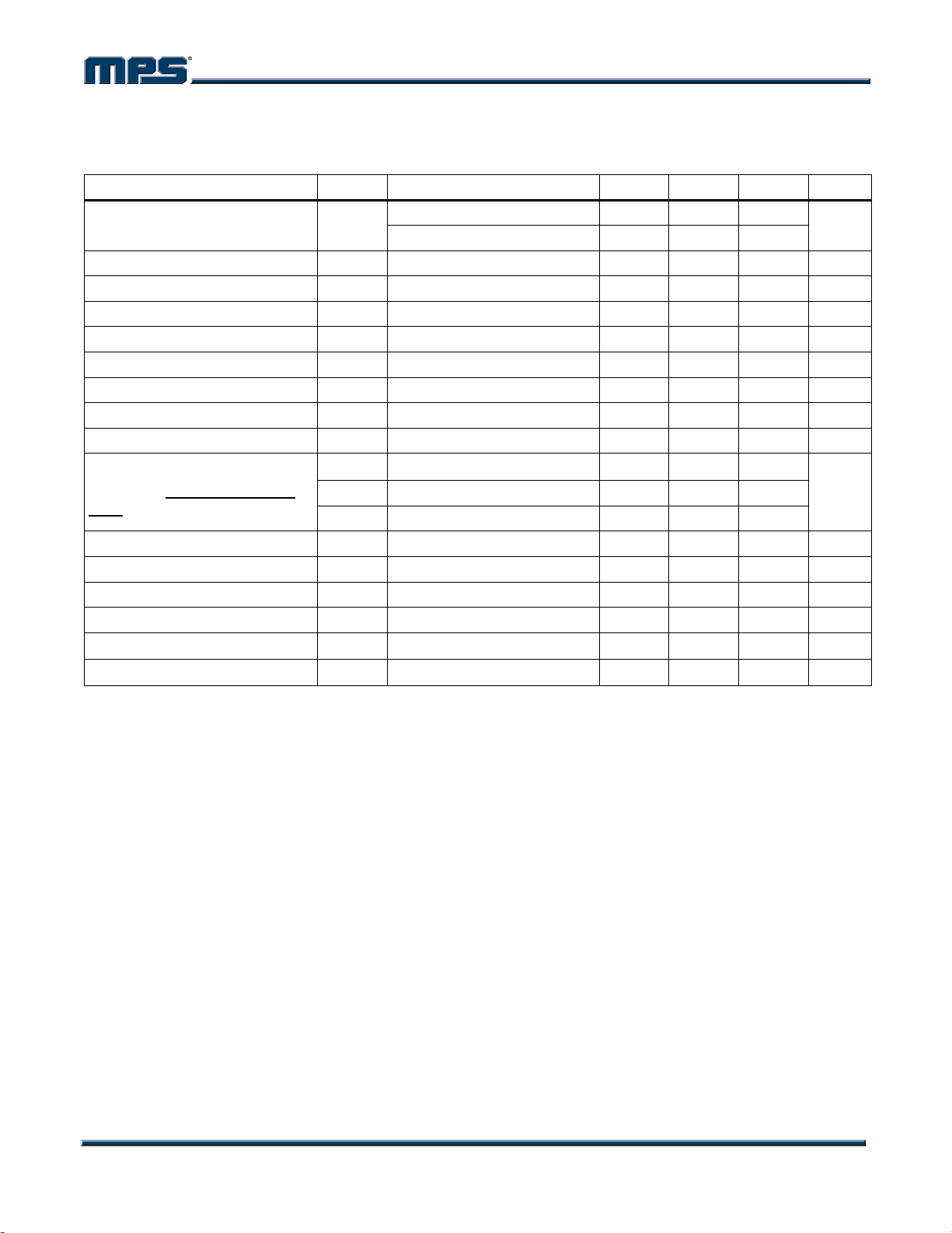
ELECTRICAL CHARACTERISTICS
VEN = V
Parameter Symbol Condition Min Typ Max Units
Startup Supply Voltage VST
Output Voltage Range V
Supply Current (Shutdown) VEN = V
Supply Current VFB = 1.3V 360 A
Feedback Voltage VFB 1.15 1.19 1.23 V
Feedback Input Current VFB = 1.19V 50 nA
Switching Frequency fSW 410 550 690 KHz
Maximum Duty Cycle D
EN Input Low Voltage 0.4 V
EN Input High Voltage
(see Chart EN high voltage vs
Input for details)
EN Pull Down Resistor 1 m
Low-Side On Resistance
Low-Side Current Limit I
High-Side On Resistance
Thermal Shutdown
Thermal Shutdown Hysteresis
Note:
5) Guaranteed by design, not tested.
= 3.3V, TA = +25°C, unless otherwise noted.
OUT
I
= 0mA 1.5 1.6 1.8
LOAD
R
= 50 1.65
LOAD
2.5 6.0 V
OUT
OUT
80 90 95 %
MAX
V
=1.8V
IN
VIN =3.3V 1.65
V
(5)
R
(5)
R
(5)
160
ONLS
1.3 A
LIM
ONHS
(5)
30
=5V 2.15
IN
V
V
= 3.3V 300 m
OUT
= 3.3V 530 700 m
OUT
V
=0V, VSW = 5V 0.15 0.5 A
1.05
V
°C
°C
MP3410 Rev. 1.12 www.MonolithicPower.com 3
6/30/2011 MPS Proprietary Information. Patent Protected. Unauthorized Photocopy and Duplication Prohibited.
© 2011 MPS. All Rights Reserved.
 Loading...