

MPS MP2161GJ Schematic [ru]

MP2161
Synchronous Step Down Switcher
The Future of Analog IC Technology
2A, 6V, 1.5MHz, 17μA IQ, COT
In 8-pin TSOT23
DESCRIPTION
The MP2161 is a monolithic step-down switch
mode converter with built-in internal power
MOSFETs. It achieves 2A continuous output
current from a 2.5V to 6V input voltage with
excellent load and line regulation. The output
voltage can be regulated as low as 0.6V.
The Constant-On-Time control scheme
provides fast transient response and eases loop
stabilization. Fault condition protection includes
cycle-by-cycle current limiting and thermal
shutdown.
The MP2161 is available in the small TSOT23-8
package and requires a minimum number of
readily available standard external components.
The MP2161 is ideal for a wide range of
applications including High Performance DSPs,
FPGAs, PDAs, and portable instruments.
FEATURES
• Very Low I
• Default 1.5MHz Switching Frequency
• EN and Power Good for Power Sequencing
• Wide 2.5V to 6V Operating Input Range
Output Adjustable from 0.6V
• Up to 2A Output Current
• 100% Duty Cycle in Dropout
• 100m and 60m Internal Power MOSFET
Switches
• Cycle-by-Cycle Over Current Protection
• Short Circuit Protect with Hiccup Mode
• Stable with Low ESR Output Ceramic
Capacitors
• Available in a TSOT23-8 Package
: 17A
Q
APPLICATIONS
• Wireless/Networking Cards
• Portable Instruments
• Battery Powered Devices
• Low Voltage I/O System Power
All MPS parts are lead-free and adhere to the RoHS directive. For MPS green
status, please visit MPS website under Products, Quality Assurance page.
“MPS” and “The Future of Analog IC Technology” are registered trademarks of
Monolithic Power Systems, Inc.
TYPICAL APPLICATION
MP2161 Rev. 1.03 www.MonolihicPower.com 1
9/6/2013 MPS Proprietary Information. Patent Protected. Unauthorized Photocopy and Duplication Prohibited.
© 2013 MPS. All Rights Reserved.
MP2161 – 2A, 6V, 1.5MHz SYNCHRONOUS STEP-DOWN SWITCHER
ORDERING INFORMATION
Part Number* Package Top Marking
MP2161GJ TSOT23-8 AEB
* For Tape & Reel, add suffix –Z (e.g. MP2161GJ–Z);
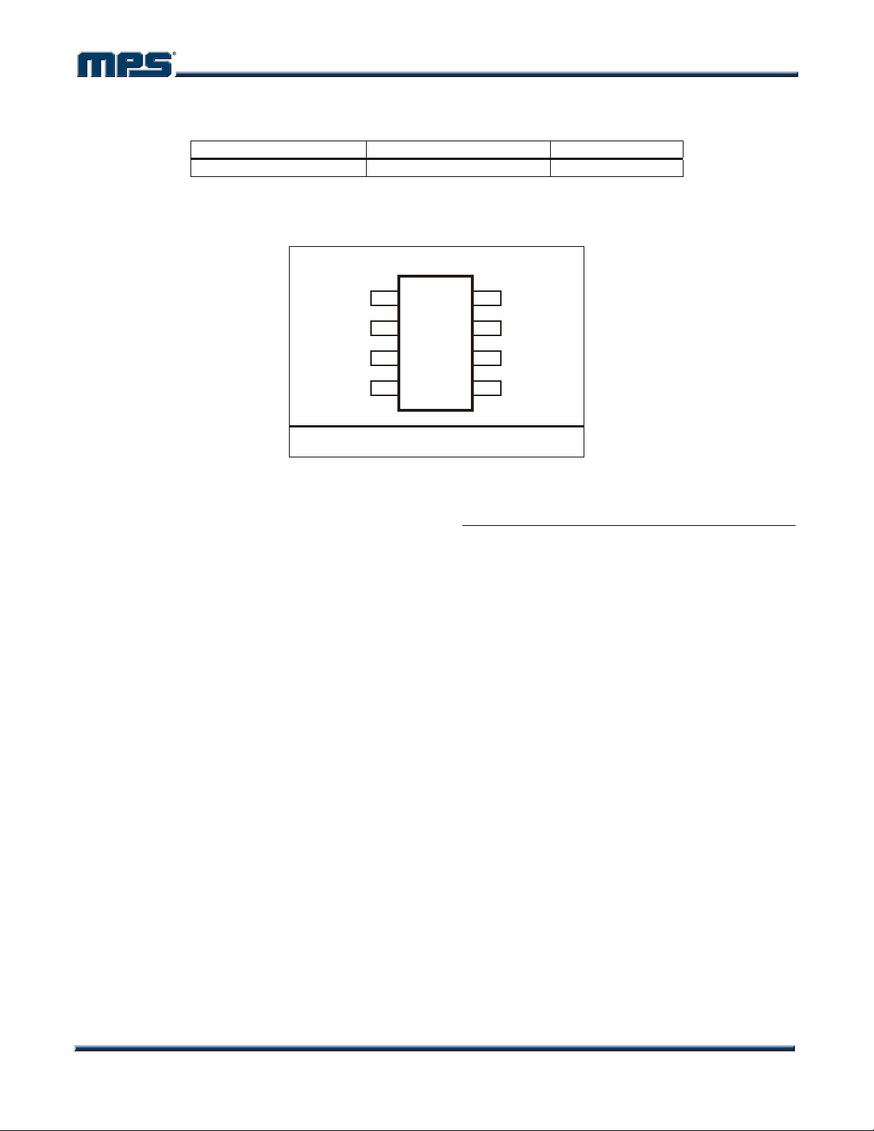
PACKAGE REFERENCE
TOP VIEW
PG
1
VIN
2
SW
3
PGND
4
TSOT23-8
ABSOLUTE MAXIMUM RATINGS
(1)
Supply Voltage VIN...................................... 6.5V
V
......................................................................
SW
-0.3V (-1.5V for <10ns) to 6.5V (7V for <10ns)
All Other Pins................................-0.3V to 6.5 V
Junction Temperature...............................150°C
Lead Temperature ....................................260°C
Continuous Power Dissipation (T
= +25°C)
A
(2)
……….….. ............................................... 1.25W
Storage Temperature............... -65°C to +150°C
Recommended Operating Conditions
(3)
Supply Voltage VIN.............................2.5V to 6V
Operating Junction Temp. (T
). -40°C to +125°C
J
EN
8
FB
7
AGND
6
OUT
5
Thermal Resistance
(4)
θ
JA
θJC
TSOT23-8.............................. 100 ..... 55... °C/W
Notes:
1) Exceeding these ratings may damage the device.
2) The maximum allowable power dissipation is a function of the
maximum junction temperature T
ambient thermal resistance
. The maximum allowable continuous power dissipation at
T
A
any ambient temperature is calculated by P
(MAX)-TA)/JA. Exceeding the maximum allowable power
dissipation will cause excessive die temperature, and the
regulator will go into thermal shutdown. Internal thermal
shutdown circuitry protects the device from permanent
damage.
3) The device is not guaranteed to function outside of its
operating conditions.
4) Measured on JESD51-7, 4-layer PCB.
(MAX), the junction-to-
J
, and the ambient temperature
JA
(MAX) = (T
D
J
MP2161 Rev. 1.03 www.MonolihicPower.com 2
9/6/2013 MPS Proprietary Information. Patent Protected. Unauthorized Photocopy and Duplication Prohibited.
© 2013 MPS. All Rights Reserved.
MP2161 – 2A, 6V, 1.5MHz SYNCHRONOUS STEP-DOWN SWITCHER
ELECTRICAL CHARACTERISTICS
(5)
VIN = 5V, TA = +25°C, unless otherwise noted.
Parameter Symbol Condition Min Typ Max Units
Feedback Voltage VFB
Feedback Current IFB V
PFET Switch On Resistance R
NFET Switch On Resistance R
DSON_P
DSON_N
Switch Leakage
PFET Current Limit 2.7 3.2 4.0 A
ON Time TON
Switching frequency Fs
Minimum Off Time T
Soft-Start Time T
MIN-OFF
SS-ON
Power Good Upper Trip Threshold PGH
Power Good Lower Trip Threshold PGL -10 %
Power Good Delay PGD 50 s
Power Good Sink Current
Capability
Power Good Logic High Voltage V
Power Good Internal Pull Up
Resistor
Under Voltage Lockout Threshold
Rising
Under Voltage Lockout Threshold
Hysteresis
V
PG-L
PG-H
R
PG
2.15 2.3 2.45 V
260 mV
EN Input Logic Low Voltage 0.4 V
EN Input Logic High Voltage 1.2 V
EN Input Current
Supply Current (Shutdown) VEN=0V, VIN=3V 20 100 nA
Supply Current (Quiescent) VEN=2V, VFB=0.63V, VIN=5V 17 20 A
Thermal Shutdown
Thermal Hysteresis
Notes:
5) Guaranteed by design.
6) Guaranteed by characterization test.
(5)
150
(5)
30
2.5V VIN 6V -3% 0.600 +3%
TA=-40oC to +85oC
= 0.6V 10 50 nA
FB
(6)
-3.5% +3.5%
V/%
100 m
60 m
V
= 0V, V
EN
V
= 0V and 6V
SW
VIN=5V, V
V
=3.6V, V
IN
V
=1.2V -20% 1500 +20% kHz/%
OUT
T
=-40oC to +85oC
A
= 6V
IN
=1.2V 185
OUT
=1.2V 245
OUT
(6)
-25% 1500 +25% kHz/%
0 1 A
ns
60 ns
1.5 ms
FB voltage respect to the
regulation
+10 %
Sink 1mA 0.4 V
VIN=5V, VFB=0.6V 4.9 V
550 k
VEN=2V 1.5 A
V
=0V 0 A
EN
°C
°C
MP2161 Rev. 1.03 www.MonolihicPower.com 3
9/6/2013 MPS Proprietary Information. Patent Protected. Unauthorized Photocopy and Duplication Prohibited.
© 2013 MPS. All Rights Reserved.
MP2161 – 2A, 6V, 1.5MHz SYNCHRONOUS STEP-DOWN SWITCHER
TYPICAL PERFORMANCE CHARACTERISTICS
VIN = 5V, V
= 1.2V, L = 1.0µH, TA = +25ºC, unless otherwise noted.
OUT
Quiescent Current vs.
Input Voltage
40
30
20
10
0
2 2.5 3 3 .5 4 4.5 5 5.5 6
INPUT VOLTAGE (V)
Shutdown Current vs.
Input Voltage
0.003
0.0025
0.002
0.0015
0.001
0.0005
0
2 2.5 3 3.5 4 4.5 5 5.5 6
INPUT VOLTAGE (V)
Line Regulation Case Temp Rise
1.00
0.80
0.60
0.40
0.20
0.00
-0.20
-0.40
-0.60
-0.80
-1.00
Load=1A
Load=0A
23456
INPUT VOLTAGE (V)
Load=2A
VIN=3V, V
50
45
40
35
30
25
20
15
10
5
0
0 0.5 1 1.5 2 2.5
OUT
OUTPUT CURRE NT (A)
=1.2V
Load Regulation
2.00
1.50
1.00
0.50
0.00
-0.50
-1.00
-1.50
-2.00
VIN=5V
=6V
V
IN
0 0.5 1 1.5 2 2.5
LOAD CURRENT (A)
Case Temp Rise
VIN=5V, V
50
45
40
35
30
25
20
15
10
5
0
0 0.5 1 1.5 2 2.5
=3.3V
OUT
OUTPUT CURRE NT (A)
Efficiency
100
VIN=3.3V
95
90
85
80
75
70
65
60
55
50
=5V
V
IN
1 10 100 1000 10000
LOAD CURRENT(mA)
V
=6V
IN
Efficiency
5/3.3VIN to 1.8V
100
90
80
VIN=5V VIN=3.3V
70
60
50
0 0.5 1 1.5 2 2.5
I
OUT
OUT
(A)
Efficiency
5VIN to 3.3V
100
90
80
70
60
50
0 0.5 1 1.5 2 2.5
OUT
I
OUT
(A)
MP2161 Rev. 1.03 www.MonolihicPower.com 4
9/6/2013 MPS Proprietary Information. Patent Protected. Unauthorized Photocopy and Duplication Prohibited.
© 2013 MPS. All Rights Reserved.
MP2161 – 2A, 6V, 1.5MHz SYNCHRONOUS STEP-DOWN SWITCHER
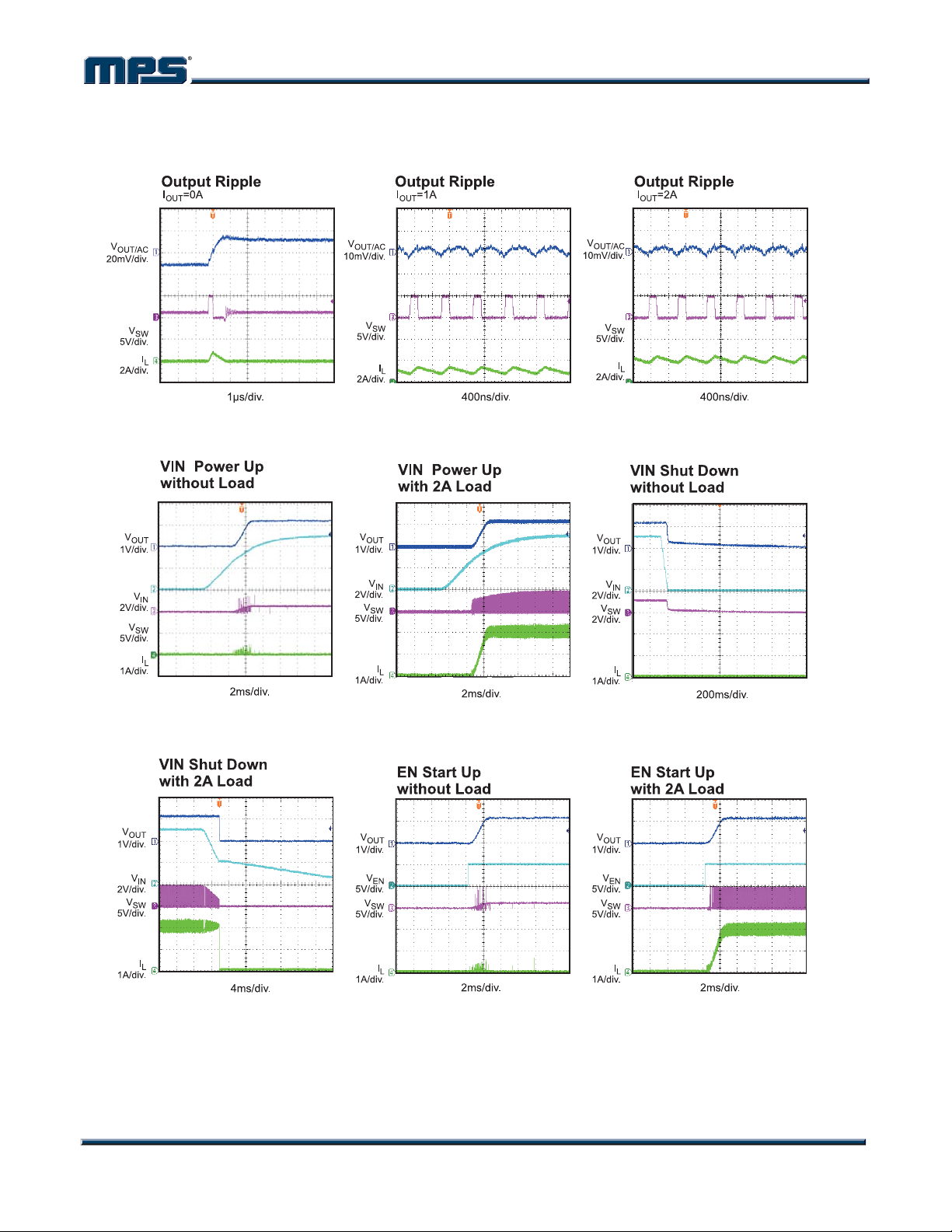
TYPICAL PERFORMANCE CHARACTERISTICS (continued)
VIN = 5V, V
= 1.2V, L = 1.0µH, TA = +25ºC, unless otherwise noted.
OUT
MP2161 Rev. 1.03 www.MonolihicPower.com 5
9/6/2013 MPS Proprietary Information. Patent Protected. Unauthorized Photocopy and Duplication Prohibited.
© 2013 MPS. All Rights Reserved.
 Loading...