

Page 1
MP1584
3A, 1.5MHz, 28V
Step-Down Converter
The Future of Analog IC Technology
DESCRIPTION
The MP1584 is a high frequency step-down
switching regulator with an integrated internal
high-side high voltage power MOSFET. It
provides 3A output with current mode control for
fast loop response and easy compensation.
The wide 4.5V to 28V input range accommodates
a variety of step-down applications, including
those in an automotive input environment. A
100µA operational quiescent current allows use in
battery-powered applications.
High power conversion efficiency over a wide
load range is achieved by scaling down the
switching frequency at light load condition to
reduce the switching and gate driving losses.
The frequency foldback helps prevent inductor
current runaway during startup and thermal
shutdown provides reliable, fault tolerant
operation.
By switching at 1.5MHz, the MP1584 is able to
prevent EMI (Electromagnetic Interference) noise
problems, such as those found in AM radio and
ADSL applications.
FEATURES
Wide 4.5V to 28V Operating Input Range
Programmable Switching Frequency from
100kHz to 1.5MHz
High-Efficiency Pulse Skipping Mode for
Light Load
Ceramic Capacitor Stable
Internal Soft-Start
Internally Set Current Limit without a
Current Sensing Resistor
Available in SOIC8E Package.
APPLICATIONS
High Voltage Power Conversion
Automotive Systems
Industrial Power Systems
Distributed Power Systems
Battery Powered Systems
“MPS” and “The Future of Analog IC Technology” are Registered Trademarks of
Monolithic Power Systems, Inc.
The MP1584 is available in a thermally enhanced
SOIC8E package.
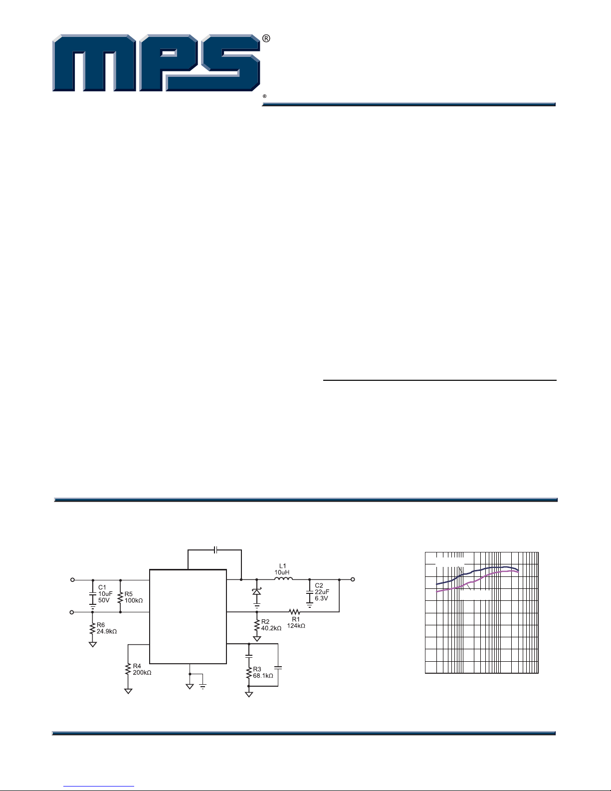
TYPICAL APPLICATION
C4
100nF
8
V
IN
EN
MP1584 Rev. 1.0 www.MonolithicPower.com 1
8/8/2011 MPS Proprietary Information. Unauthorized Photocopy and Duplication Prohibited.
© 2011 MPS. All Rights Reserved.
7
2
6
VIN
EN
FREQ
BST
MP1584
GND
5
SW
FB
COMP
1
D1
4
3
C3
220pF
C6
NS
V
OUT
3.3V
Efficiency Curve
(fSW=500kHz)
100
VIN=12V
90
80
70
60
50
40
EFFICIENCY (%)
30
20
10
0
0.01 0.1 1 10
VIN=24V
OUTPUT CURRENT (A)
Page 2
MP1584 – 3A, 1.5MHz, 28V STEP-DOWN CONVERTER
ORDERING INFORMATION
Part Number* Package Top Marking Free Air Temperature (TA)
MP1584EN
SOIC8E
MP1584EN
–20C to +85C
* For Tape & Reel, add suffix –Z (e.g. MP1584EN–Z);
For RoHS Compliant Packaging, add suffix –LF. (e.g. MP1584EN–LF–Z)
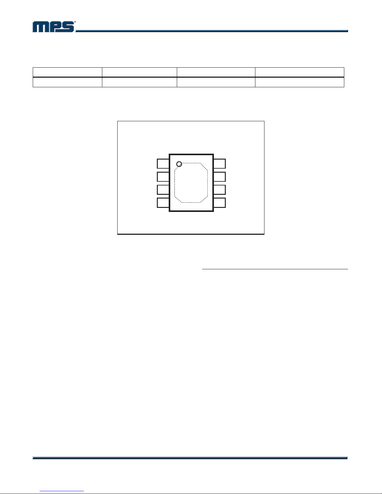
PACKAGE REFERENCE
TOP VIEW
SW
COMP
ABSOLUTE MAXIMUM RATINGS
EN
FB
1
2
3
4
(1)
Supply Voltage (VIN) ..................... –0.3V to +30V
Switch Voltage (V
) ............ –0.3V to VIN + 0.3V
SW
BST to SW ..................................... –0.3V to +6V
All Other Pins ................................. –0.3V to +6V
Continuous Power Dissipation (T
+25°C)
(2)
=
A
............................................................. 2.5W
Junction Temperature ............................... 150C
Lead Temperature .................................... 260C
Storage Temperature .............. –65°C to +150C
Recommended Operating Conditions
Supply Voltage V
Output Voltage V
........................... 4.5V to 28V
IN
......................... 0.8V to 25V
OUT
(3)
BST
8
VIN
7
FREQ
6
GND
5
Operating Junct. Temp (T
Thermal Resistance
) ..... –20C to +125C
J
(4)
θ
JA
θJC
SOIC8E .................................. 50 ...... 10 ... C/W
Notes:
1) Exceeding these ratings may damage the device.
2) The maximum allowable power dissipation is a function of the
maximum junction temperature T
ambient thermal resistance
. The maximum allowable continuous power dissipation at
T
A
any ambient temperature is calculated by P
)/ JA. Exceeding the maximum allowable power dissipation
T
A
will cause excessive die temperature, and the regulator will go
into thermal shutdown. Internal thermal shutdown circuitry
protects the device from permanent damage.
3) The device is not guaranteed to function outside of its
operating conditions.
4) Measured on JESD51-7, 4-layer PCB.
(MAX), the junction-to-
J
, and the ambient temperature
JA
(MAX)=(TJ(MAX)-
D
MP1584 Rev. 1.0 www.MonolithicPower.com 2
8/8/2011 MPS Proprietary Information. Unauthorized Photocopy and Duplication Prohibited.
© 2011 MPS. All Rights Reserved.
Page 3
MP1584 – 3A, 1.5MHz, 28V STEP-DOWN CONVERTER
)
(5)
(5)
(5)
(5)
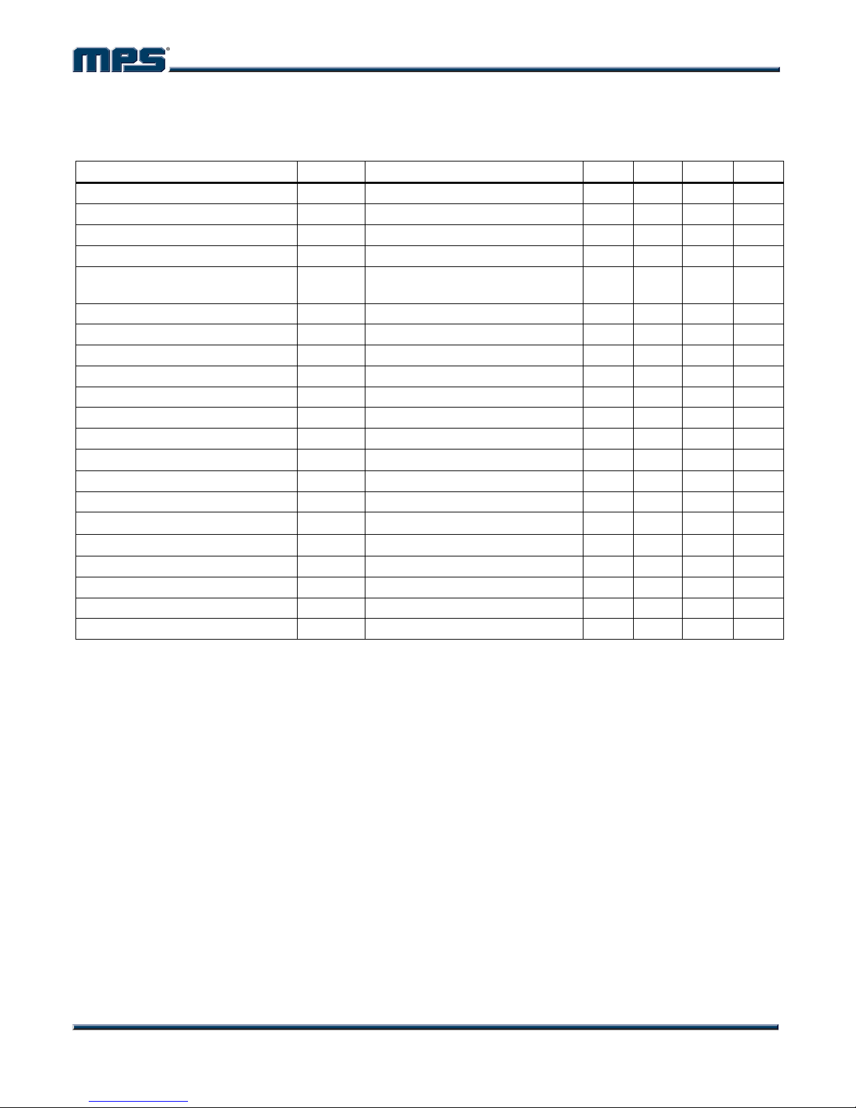
ELECTRICAL CHARACTERISTICS
VIN = 12V, VEN = 2.5V, V
Parameter Symbol Condition Min Typ Max Units
Feedback Voltage VFB 4.5V < VIN < 28V 0.776 0.8 0.824 V
Upper Switch On Resistance R
Upper Switch Leakage VEN = 0V, VSW = 0V, VIN = 28V 1 A
Current Limit 4.0 4.7 A
COMP to Current Sense
Transconductance
Error Amp Voltage Gain
Error Amp Transconductance I
Error Amp Min Source current VFB = 0.7V 5 µA
Error Amp Min Sink current VFB = 0.9V –5 µA
VIN UVLO Threshold 2.7 3.0 3.3 V
VIN UVLO Hysteresis 0.35 V
Soft-Start Time
Oscillator Frequency R
Shutdown Supply Current VEN = 0V 12 20 µA
Quiescent Supply Current No load, VFB = 0.9V 100 125 µA
Thermal Shutdown 150
Thermal Shutdown Hysteresis 15
Minimum Off Time
Minimum On Time
EN Up Threshold 1.35 1.5 1.65 V
EN Hysteresis 300 mV
Note:
5) Guaranteed by design.
0V < VFB < 0.8V 1.5 ms
100 ns
100 ns
= 1.4V, TA= +25C, unless otherwise noted.
COMP
V
DS(ON
G
9 A/V
CS
– VSW = 5V 150 m
BST
200 V/V
= ±3µA 40 60 80 µA/V
COMP
= 100k 900 kHz
FREQ
C
C
MP1584 Rev. 1.0 www.MonolithicPower.com 3
8/8/2011 MPS Proprietary Information. Unauthorized Photocopy and Duplication Prohibited.
© 2011 MPS. All Rights Reserved.
Page 4
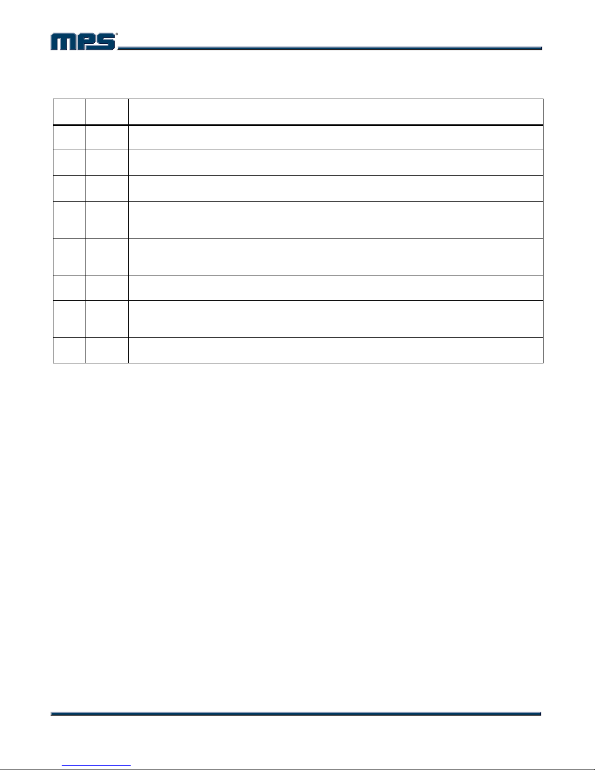
PIN FUNCTIONS
MP1584 – 3A, 1.5MHz, 28V STEP-DOWN CONVERTER
SOIC
Pin #
Name Description
1 SW
2 EN
3 COMP
4 FB
GND
5
Exposed
Pad
6 FREQ
7 VIN
8 BST
Switch Node. This is the output from the high-side switch. A low forward drop Schottky diode to
ground is required. The diode must be close to the SW pins to reduce switching spikes.
Enable Input. Pulling this pin below the specified threshold shuts the chip down. Pulling it up
above the specified threshold or leaving it floating enables the chip.
Compensation. This node is the output of the error amplifier. Control loop frequency
compensation is applied to this pin.
Feedback. This is the input to the error amplifier. The output voltage is set by a resistive divider
connected between the output and GND which scales down V
equal to the internal +0.8V
OUT
reference.
Ground. It should be connected as close as possible to the output capacitor to shorten the high
current switch paths. Connect exposed pad to GND plane for optimal thermal performance.
Switching Frequency Program Input. Connect a resistor from this pin to ground to set the
switching frequency.
Input Supply. This supplies power to all the internal control circuitry, both BS regulators and the
high-side switch. A decoupling capacitor to ground must be placed close to this pin to minimize
switching spikes.
Bootstrap. This is the positive power supply for the internal floating high-side MOSFET driver.
Connect a bypass capacitor between this pin and SW pin.
MP1584 Rev. 1.0 www.MonolithicPower.com 4
8/8/2011 MPS Proprietary Information. Unauthorized Photocopy and Duplication Prohibited.
© 2011 MPS. All Rights Reserved.
Page 5
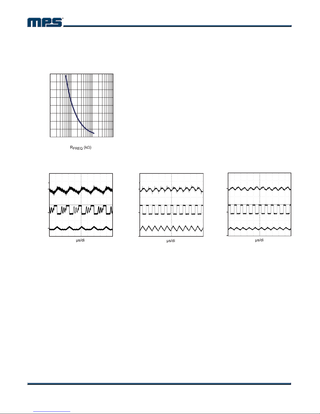
MP1584 – 3A, 1.5MHz, 28V STEP-DOWN CONVERTER
TYPICAL PERFORMANCE CHARACTERISTICS
VIN = 12V, V
Oscillating Frequency
vs. R
1600
1400
1200
1000
800
600
400
200
OSCILLATING FREQUENCY (kHZ)
0
10 100 1000 10000
Steady State
I
OUT
V
OUT
AC Coupled
10mV/div.
=5V, C1 = 10µF, C2 = 22µF, L1= 10µH, TA = +25C, unless otherwise noted.
OUT
freq
Steady State
I
OUT
V
OUT
=2A, fSW=500kHz
=0.1A, fSW=500kHz
V
OUT
AC Coupled
10mV/div.
Steady State
I
=1A, fSW=500kHz
OUT
AC Coupled
10mV/div.
V
SW
10V/div.
1A/div.
V
V
SW
10V/div.
I
L
I
L
1 v.
1A/div.
2 v.
SW
10V/div.
2A/div.
I
L
v.
2
MP1584 Rev. 1.0 www.MonolithicPower.com 5
8/8/2011 MPS Proprietary Information. Unauthorized Photocopy and Duplication Prohibited.
© 2011 MPS. All Rights Reserved.
Page 6
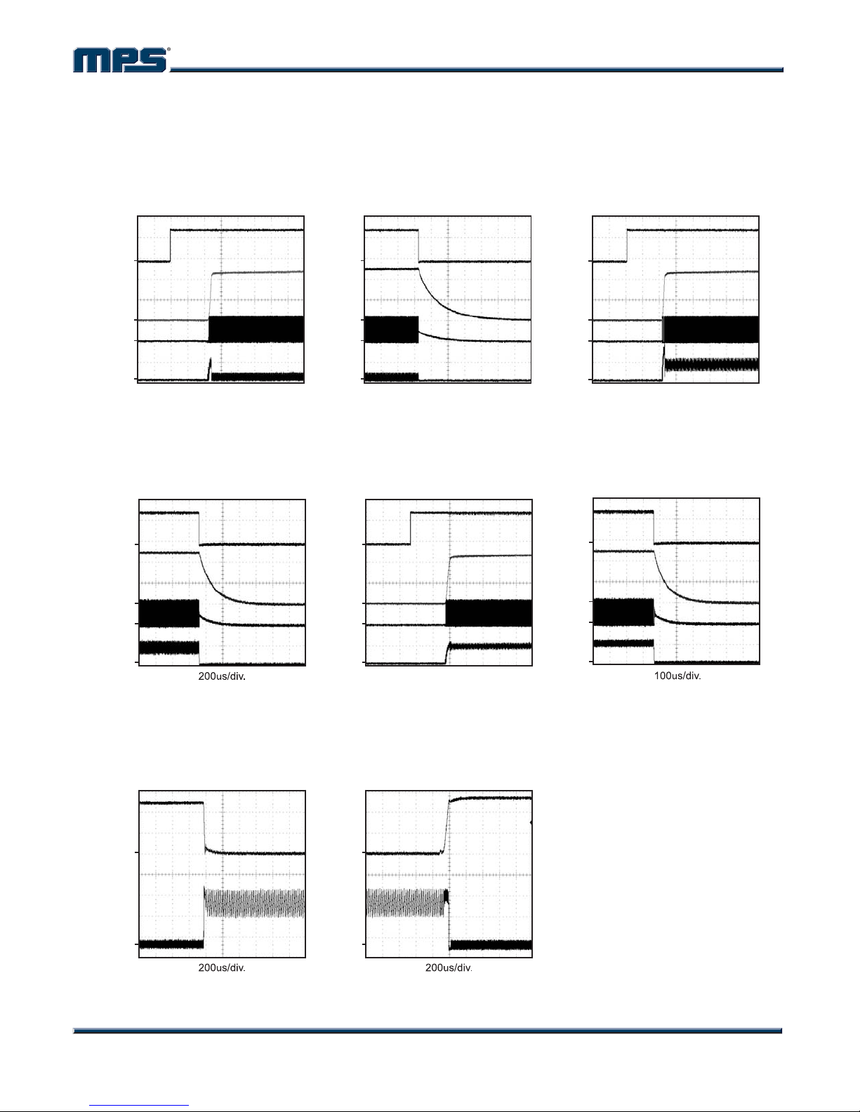
MP1584 – 3A, 1.5MHz, 28V STEP-DOWN CONVERTER
TYPICAL PERFORMANCE CHARACTERISTICS (continued)
VIN = 12V, C1 = 10µF, C2 = 22µF, L1 = 10µH, fSW=500kHz, and TA = +25C, unless otherwise noted.
V
5V/div.
Startup
I
OUT
EN
= 0.1A
V
5V/div.
EN
Shutdown
I
= 0.1A
OUT
V
5V/div.
Startup
I
OUT
EN
= 1A
V
OUT
2V/div.
V
10V/div.
1A/div.
V
5V/div.
V
OUT
2V/div.
V
10V/div.
1A/div.
SW
I
L
Shutdown
I
OUT
EN
SW
I
L
= 1A
5ms/div.
V
OUT
2V/div.
V
SW
10V/div.
1A/div.
V
5V/div.
V
OUT
2V/div.
V
10V/div.
2A/div.
I
L
Startup
I
EN
SW
I
L
OUT
= 2A
1ms/div.
5ms/div.
V
OUT
2V/div.
V
SW
10V/div.
1A/div.
V
5V/div.
V
OUT
2V/div.
V
SW
10V/div.
2A/div.
I
L
Shutdown
I
OUT
EN
I
L
5ms/div.
= 2A
Short Circuit Entry
I
= 0.1A to Short
OUT
V
OUT
2V/div.
I
L
1A/div.
MP1584 Rev. 1.0 www.MonolithicPower.com 6
8/8/2011 MPS Proprietary Information. Unauthorized Photocopy and Duplication Prohibited.
© 2011 MPS. All Rights Reserved.
Short Circuit Recovery
I
= Short to 0.1A
OUT
V
OUT
2V/div.
I
L
1A/div.
Page 7
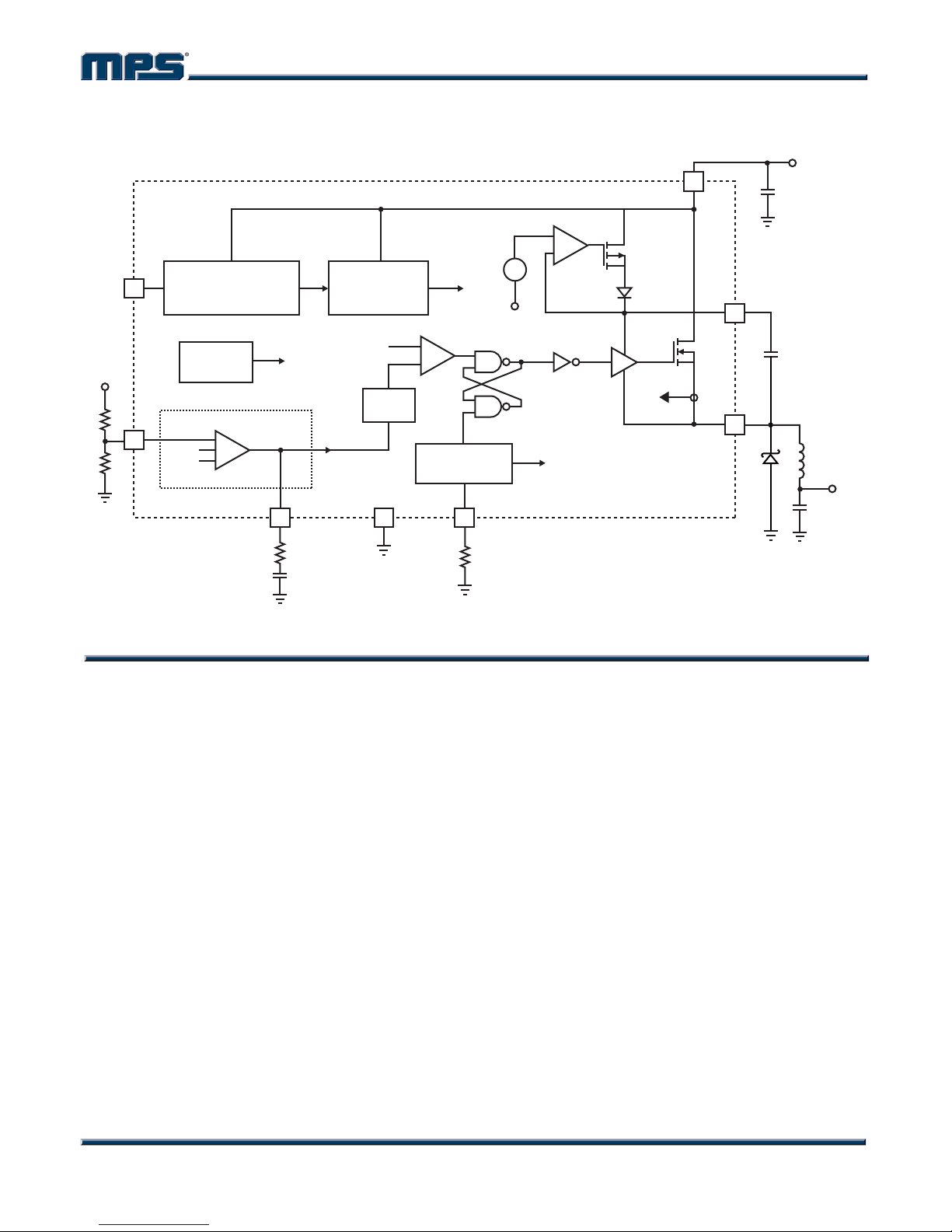
BLOCK DIAGRAM
EN
REFERENCE UVLO/
THERMAL
SHUTDOWN
INTERNAL
REGULATORS
MP1584 – 3A, 1.5MHz, 28V STEP-DOWN CONVERTER
V
IN
2.6V
5V
+
--
SW
VIN
+
--
BST
--
+
Shift
OSCILLATOR
GND
V
OUT
FB
1.5ms SS
SS
0V8
Gm Error Amp
--
+
SS
COMP
COMP
I
SW
Level
Figure 1—Functional Block Diagram
OPERATION
The MP1584 is a variable frequency,
non-synchronous, step-down switching
regulator with an integrated high-side high
voltage power MOSFET. It provides a highly
efficient solution with current mode control for
fast loop response and easy compensation. It
features a wide input voltage range, internal
soft-start control and precision current limiting.
Its very low operational quiescent current
makes it suitable for battery powered
applications.
I
SW
CLK
FREQ
SW
PWM Control
At moderate to high output current, the MP1584
operates in a fixed frequency, peak current
control mode to regulate the output voltage. A
PWM cycle is initiated by the internal clock. The
power MOSFET is turned on and remains on
until its current reaches the value set by the
COMP voltage. When the power switch is off, it
remains off for at least 100ns before the next
cycle starts. If, in one PWM period, the current
in the power MOSFET does not reach the
COMP set current value, the power MOSFET
remains on, saving a turn-off operation.
V
OUT
MP1584 Rev. 1.0 www.MonolithicPower.com 7
8/8/2011 MPS Proprietary Information. Unauthorized Photocopy and Duplication Prohibited.
© 2011 MPS. All Rights Reserved.
Page 8

MP1584 – 3A, 1.5MHz, 28V STEP-DOWN CONVERTER
Error Amplifier
The error amplifier compares the FB pin voltage
with the internal reference (REF) and outputs a
current proportional to the difference between
the two. This output current is then used to
charge the external compensation network to
form the COMP voltage, which is used to
control the power MOSFET current.
During operation, the minimum COMP voltage
is clamped to 0.9V and its maximum is clamped
to 2.0V. COMP is internally pulled down to GND
in shutdown mode. COMP should not be pulled
up beyond 2.6V.
Internal Regulator
Most of the internal circuitries are powered from
the 2.6V internal regulator. This regulator takes
the VIN input and operates in the full VIN range.
When VIN is greater than 3.0V, the output of
the regulator is in full regulation. When VIN is
lower than 3.0V, the output decreases.
Enable Control
The MP1584 has a dedicated enable control pin
(EN). With high enough input voltage, the chip
can be enabled and disabled by EN which has
positive logic. Its falling threshold is a precision
1.2V, and its rising threshold is 1.5V (300mV
higher).
When floating, EN is pulled up to about 3.0V by
an internal 1µA current source so it is enabled.
To pull it down, 1µA current capability is
needed.
When EN is pulled down below 1.2V, the chip is
put into the lowest shutdown current mode.
When EN is higher than zero but lower than its
rising threshold, the chip is still in shutdown
mode but the shutdown current increases
slightly.
Under-Voltage Lockout (UVLO)
Under-voltage lockout (UVLO) is implemented
to protect the chip from operating at insufficient
supply voltage. The UVLO rising threshold is
about 3.0V while its falling threshold is a
consistent 2.6V.
Internal Soft-Start
The soft-start is implemented to prevent the
converter output voltage from overshooting
during startup. When the chip starts, the
internal circuitry generates a soft-start voltage
(SS) ramping up from 0V to 2.6V. When it is
lower than the internal reference (REF), SS
overrides REF so the error amplifier uses SS as
the reference. When SS is higher than REF,
REF regains control.
Thermal Shutdown
Thermal shutdown is implemented to prevent
the chip from operating at exceedingly high
temperatures. When the silicon die temperature
is higher than its upper threshold, it shuts down
the whole chip. When the temperature is lower
than its lower threshold, the chip is enabled
again.
Floating Driver and Bootstrap Charging
The floating power MOSFET driver is powered
by an external bootstrap capacitor. This floating
driver has its own UVLO protection. This
UVLO’s rising threshold is 2.2V with a threshold
of 150mV.
The bootstrap capacitor is charged and
regulated to about 5V by the dedicated internal
bootstrap regulator. When the voltage between
the BST and SW nodes is lower than its
regulation, a PMOS pass transistor connected
from VIN to BST is turned on. The charging
current path is from VIN, BST and then to SW.
External circuit should provide enough voltage
headroom to facilitate the charging.
As long as VIN is sufficiently higher than SW,
the bootstrap capacitor can be charged. When
the power MOSFET is ON, VIN is about equal
to SW so the bootstrap capacitor cannot be
charged. When the external diode is on, the
difference between VIN and SW is largest, thus
making it the best period to charge. When there
is no current in the inductor, SW equals the
output voltage V
V
and V
IN
OUT
so the difference between
OUT
can be used to charge the
bootstrap capacitor.
MP1584 Rev. 1.0 www.MonolithicPower.com 8
8/8/2011 MPS Proprietary Information. Unauthorized Photocopy and Duplication Prohibited.
© 2011 MPS. All Rights Reserved.
Page 9

MP1584 – 3A, 1.5MHz, 28V STEP-DOWN CONVERTER
At higher duty cycle operation condition, the
time period available to the bootstrap charging
is less so the bootstrap capacitor may not be
sufficiently charged.
In case the internal circuit does not have
sufficient voltage and the bootstrap capacitor is
not charged, extra external circuitry can be
used to ensure the bootstrap voltage is in the
normal operational region. Refer to External
Bootstrap Diode in Application section.
The DC quiescent current of the floating driver
is about 20µA. Make sure the bleeding current
at the SW node is higher than this value, such
that:
V
I
O
O
)2R1R(
A20
Current Comparator and Current Limit
The power MOSFET current is accurately
sensed via a current sense MOSFET. It is then
fed to the high speed current comparator for the
current mode control purpose. The current
comparator takes this sensed current as one of
its inputs. When the power MOSFET is turned
on, the comparator is first blanked till the end of
the turn-on transition to avoid noise issues. The
comparator then compares the power switch
current with the COMP voltage. When the
sensed current is higher than the COMP
voltage, the comparator output is low, turning
off the power MOSFET. The cycle-by-cycle
maximum current of the internal power
MOSFET is internally limited.
Startup and Shutdown
If both VIN and EN are higher than their
appropriate thresholds, the chip starts. The
reference block starts first, generating stable
reference voltage and currents, and then the
internal regulator is enabled. The regulator
provides stable supply for the remaining
circuitries.
While the internal supply rail is up, an internal
timer holds the power MOSFET OFF for about
50µs to blank the startup glitches. When the
internal soft-start block is enabled, it first holds
its SS output low to ensure the remaining
circuitries are ready and then slowly ramps up.
Three events can shut down the chip: EN low,
VIN low and thermal shutdown. In the shutdown
procedure, power MOSFET is turned off first to
avoid any fault triggering. The COMP voltage
and the internal supply rail are then pulled
down.
Programmable Oscillator
The MP1584 oscillating frequency is set by an
external resistor, R
ground. The value of R
from:
R(k)
freq
from the FREQ pin to
freq
can be calculated
freq
180000
f(kHz)
s
1.1
MP1584 Rev. 1.0 www.MonolithicPower.com 9
8/8/2011 MPS Proprietary Information. Unauthorized Photocopy and Duplication Prohibited.
© 2011 MPS. All Rights Reserved.
Page 10

MP1584 – 3A, 1.5MHz, 28V STEP-DOWN CONVERTER
APPLICATION INFORMATION
COMPONENT SELECTION
Setting the Output Voltage
The output voltage is set using a resistive
voltage divider from the output voltage to FB pin.
The voltage divider divides the output voltage
down to the feedback voltage by the
ratio:
2R
VV
OUTFB
Thus the output voltage is:
VV
FBOUT
About 20µA current from high side BS circuitry
can be seen at the output when the MP1584 is
at no load. In order to absorb this small amount
of current, keep R2 under 40K. A typical
value for R2 can be 40.2k. With this value, R1
can be determined by:
OUT
For example, for a 3.3V output voltage, R2 is
40.2k, and R1 is 127k.
Inductor
The inductor is required to supply constant
current to the output load while being driven by
the switched input voltage. A larger value
inductor will result in less ripple current that will
result in lower output ripple voltage. However,
the larger value inductor will have a larger
physical size, higher series resistance, and/or
lower saturation current.
2R1R
)2R1R(
2R
)k)(8.0V(25.501R
A good rule for determining the inductance to
use is to allow the peak-to-peak ripple current in
the inductor to be approximately 30% of the
maximum switch current limit. Also, make sure
that the peak inductor current is below the
maximum switch current limit. The inductance
value can be calculated by:
V
OUT
V
IN
Where V
voltage, f
V
OUT
1L
OUT is the output voltage, VIN is the input
S is the switching frequency, and IL is
1
If
LS
the peak-to-peak inductor ripple current.
Choose an inductor that will not saturate under
the maximum inductor peak current. The peak
inductor current can be calculated by:
V
OUT
V
IN
Where I
V
II
LOADLP
LOAD is the load current.
OUT
S
1Lf2
1
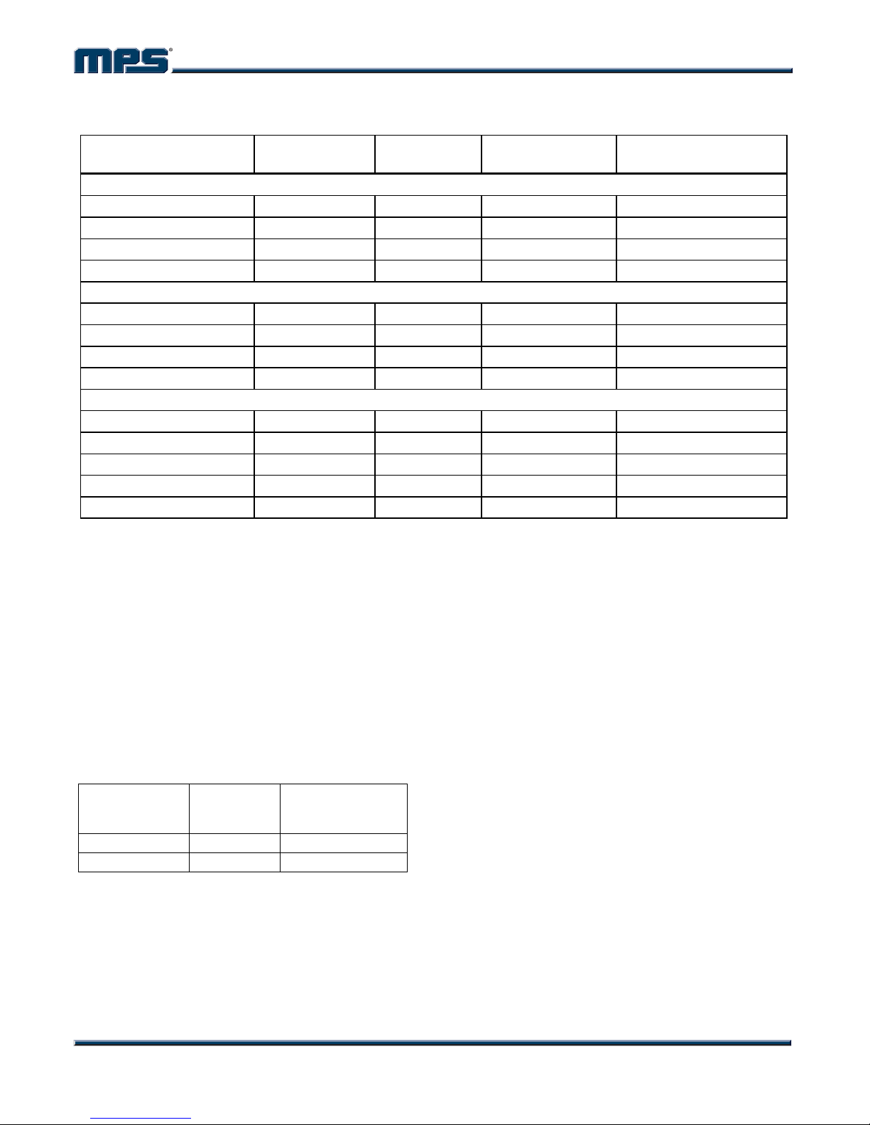
Table 1 lists a number of suitable inductors
from various manufacturers. The choice of
which style inductor to use mainly depends on
the price vs. size requirements and any EMI
requirement.
MP1584 Rev. 1.0 www.MonolithicPower.com 10
8/8/2011 MPS Proprietary Information. Unauthorized Photocopy and Duplication Prohibited.
© 2011 MPS. All Rights Reserved.
Page 11
MP1584 – 3A, 1.5MHz, 28V STEP-DOWN CONVERTER
Table 1—Inductor Selection Guide
Dimensions
Part Number Inductance (µH) Max DCR () Current Rating (A)
Wurth Electronics
7447789003 3.3 0.024 3.42 7.3x7.3x3.2
744066100 10 0.035 3.6 10x10x3.8
744771115 15 0.025 3.75 12x12x6
744771122 22 0.031 3.37 12x12x6
TDK
RLF7030T-3R3 3.3 0.02 4.1 7.3x6.8x3.2
RLF7030T-4R7 4.7 0.031 3.4 7.3x6.8x3.2
SLF10145T-100 10 0.0364 3 10.1x10.1x4.5
SLF12565T-220M3R5 22 0.0316 3.5 12.5x12.5x6.5
Toko
FDV0630-3R3M 3.3 0.031 4.3 7.7x7x3
FDV0630-4R7M 4.7 0.049 3.3 7.7x7x3
919AS-100M 10 0.0265 4.3 10.3x10.3x4.5
919AS-160M 16 0.0492 3.3 10.3x10.3x4.5
919AS-220M 22 0.0776 3 10.3x10.3x4.5
L x W x H (mm3)
Output Rectifier Diode
The output rectifier diode supplies the current to
the inductor when the high-side switch is off. To
reduce losses due to the diode forward voltage
and recovery times, use a Schottky diode.
Choose a diode whose maximum reverse
voltage rating is greater than the maximum
input voltage, and whose current rating is
greater than the maximum load current. Table 2
lists example Schottky diodes and
manufacturers.
Table 2—Diode Selection Guide
Input Capacitor
The input current to the step-down converter is
discontinuous, therefore a capacitor is required to
supply the AC current to the step-down converter
while maintaining the DC input voltage. Use low
ESR capacitors for the best performance. Ceramic
capacitors are preferred, but tantalum or low-ESR
electrolytic capacitors may also suffice.
For simplification, choose the input capacitor
with RMS current rating greater than half of the
maximum load current.
Voltage/
Diodes
B340A-13-F 40V, 3A Diodes Inc.
CMSH3-40MA 40V, 3A Central Semi
Current
Rating
MP1584 Rev. 1.0 www.MonolithicPower.com 11
8/8/2011 MPS Proprietary Information. Unauthorized Photocopy and Duplication Prohibited.
© 2011 MPS. All Rights Reserved.
Manufacturer
Page 12

MP1584 – 3A, 1.5MHz, 28V STEP-DOWN CONVERTER
The input capacitor (C1) can be electrolytic,
tantalum or ceramic. When using electrolytic or
tantalum capacitors, a small, high quality
ceramic capacitor, i.e. 0.1F, should be placed
as close to the IC as possible. When using
ceramic capacitors, make sure that they have
enough capacitance to provide sufficient charge
to prevent excessive voltage ripple at input. The
input voltage ripple caused by capacitance can
be estimated by:
OUT
V
1
IN
I
LOAD
V
IN
S
V
1Cf
V
OUT
V
IN
Output Capacitor
The output capacitor (C2) is required to
maintain the DC output voltage. Ceramic,
tantalum, or low ESR electrolytic capacitors are
recommended. Low ESR capacitors are
preferred to keep the output voltage ripple low.
The output voltage ripple can be estimated by:
OUT
1
Lf
V
V
OUT
S
V
OUT
V
IN
R
ESR
Where L is the inductor value and R
ESR is the
1
2Cf8
S
equivalent series resistance (ESR) value of the
output capacitor.
In the case of ceramic capacitors, the
impedance at the switching frequency is
dominated by the capacitance. The output
voltage ripple is mainly caused by the
capacitance. For simplification, the output
voltage ripple can be estimated by:
V
OUT
V
OUT
2
S
1
2CLf8
V
OUT
V
IN
In the case of tantalum or electrolytic capacitors,
the ESR dominates the impedance at the
switching frequency. For simplification, the
output ripple can be approximated to:
V
OUT
OUT
Lf
S
V
V
1
OUT
V
IN
R
ESR
The characteristics of the output capacitor also
affect the stability of the regulation system. The
MP1584 can be optimized for a wide range of
capacitance and ESR values.
Compensation Components
MP1584 employs current mode control for easy
compensation and fast transient response. The
system stability and transient response are
controlled through the COMP pin. COMP pin is
the output of the internal error amplifier. A
series capacitor-resistor combination sets a
pole-zero combination to control the
characteristics of the control system. The DC
gain of the voltage feedback loop is given by:
V
FB
V
OUT
Where A
200V/V; G
VEA is the error amplifier voltage gain,
CS is the current sense
transconductance, 9A/V; R
AGRA
VEACSLOADVDC
LOAD is the load
resistor value.
The system has two poles of importance. One
is due to the compensation capacitor (C3), the
output resistor of error amplifier. The other is
due to the output capacitor and the load resistor.
These poles are located at:
G
Where, G
f
1P
f
2P
EA is the error amplifier
EA
1
A3C2
R2C2
VEA
LOAD
transconductance, 60A/V.
The system has one zero of importance, due to
the compensation capacitor (C3) and the
compensation resistor (R3). This zero is located
at:
f
1Z
1
3R3C2
The system may have another zero of
importance, if the output capacitor has a large
capacitance and/or a high ESR value. The zero,
due to the ESR and capacitance of the output
capacitor, is located at:
f
ESR
1
R2C2
ESR
MP1584 Rev. 1.0 www.MonolithicPower.com 12
8/8/2011 MPS Proprietary Information. Unauthorized Photocopy and Duplication Prohibited.
© 2011 MPS. All Rights Reserved.
Page 13
MP1584 – 3A, 1.5MHz, 28V STEP-DOWN CONVERTER
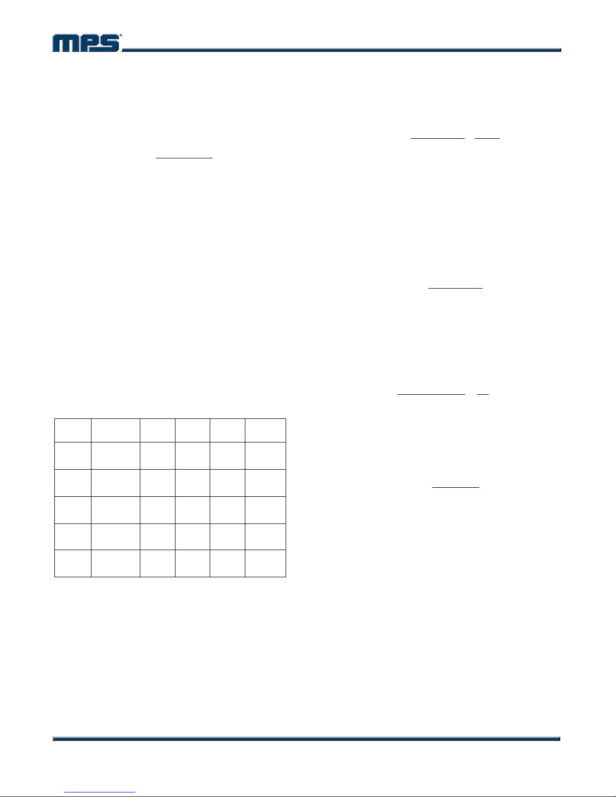
In this case (as shown in Figure 2), a third pole
set by the compensation capacitor (C6) and the
compensation resistor (R3) is used to
compensate the effect of the ESR zero on the
loop gain. This pole is located at:
f
3P
1
3R6C2
The goal of compensation design is to shape
the converter transfer function to get a desired
loop gain. The system crossover frequency
where the feedback loop has the unity gain is
important. Lower crossover frequencies result
in slower line and load transient responses,
while higher crossover frequencies could cause
system unstable. A good rule of thumb is to set
the crossover frequency to approximately onetenth of the switching frequency. The Table 3
lists the typical values of compensation
components for some standard output voltages
with various output capacitors and inductors.
The values of the compensation components
have been optimized for fast transient
responses and good stability at given conditions.
Table 3—Compensation Values for Typical
Output Voltage/Capacitor Combinations
V
OUT
(V)
1.8 4.7 47 105 100 None
L (µH)
C2
(µF)
R3
(k)
C3
(pF)
C6
1. Choose the compensation resistor (R3) to set
the desired crossover frequency. Determine the
R3 value by the following equation:
V
f2C2
Where f
3R
C is the desired crossover frequency.
GG
CSEA
OUT
C
V
FB
2. Choose the compensation capacitor (C3) to
achieve the desired phase margin. For
applications with typical inductor values, setting
the compensation zero, f
Z1, below one forth of
the crossover frequency provides sufficient
phase margin. Determine the C3 value by the
following equation:
3C
4
f3R2
C
3. Determine if the second compensation
capacitor (C6) is required. It is required if the
ESR zero of the output capacitor is located at
less than half of the switching frequency, or the
following relationship is valid:
1
R2C2
ESR
f
S
2
If this is the case, then add the second
compensation capacitor (C6) to set the pole f
P3
at the location of the ESR zero. Determine the
C6 value by the equation:
R2C
3R
ESR
2.5 4.7 - 6.8 22 54.9 220 None
3.3 6.8 -10 22 68.1 220 None
5 15 - 22 22 100 150 None
12 22 - 33 22 147 150 None
6C
To optimize the compensation components for
conditions not listed in Table 3, the following
procedure can be used.
MP1584 Rev. 1.0 www.MonolithicPower.com 13
8/8/2011 MPS Proprietary Information. Unauthorized Photocopy and Duplication Prohibited.
© 2011 MPS. All Rights Reserved.
Page 14
MP1584 – 3A, 1.5MHz, 28V STEP-DOWN CONVERTER
High Frequency Operation
The switching frequency of MP1584 can be
programmed up to 1.5MHz with an external
resistor.
With higher switching frequencies, the inductive
reactance (X
) of capacitor comes to dominate,
L
so that the ESL of input/output capacitor
determines the input/output ripple voltage at
higher switching frequency. As a result of that,
high frequency ceramic capacitor is strongly
recommended as input decoupling capacitor
and output filtering capacitor for such high
frequency operation.
Layout becomes more important when the
device switches at higher frequency. It is
essential to place the input decoupling
capacitor, catch diode and the MP1584 (Vin pin,
SW pin and PGND) as close as possible, with
traces that are very short and fairly wide. This
can help to greatly reduce the voltage spike on
SW node, and lower the EMI noise level as well.
Try to run the feedback trace as far from the
inductor and noisy power traces as possible. It
is often a good idea to run the feedback trace
on the side of the PCB opposite of the inductor
with a ground plane separating the two. The
compensation components should be placed
closed to the MP1584. Do not place the
compensation components close to or under
high dv/dt SW node, or inside the high di/dt
power loop. If you have to do so, the proper
ground plane must be in place to isolate those.
Switching loss is expected to be increased at
high switching frequency. To help to improve
the thermal conduction, a grid of thermal vias
can be created right under the exposed pad. It
is recommended that they be small (15mil
barrel diameter) so that the hole is essentially
filled up during the plating process, thus aiding
conduction to the other side. Too large a hole
can cause ‘solder wicking’ problems during the
reflow soldering process. The pitch (distance
between the centers) of several such thermal
vias in an area is typically 40mil.
External Bootstrap Diode
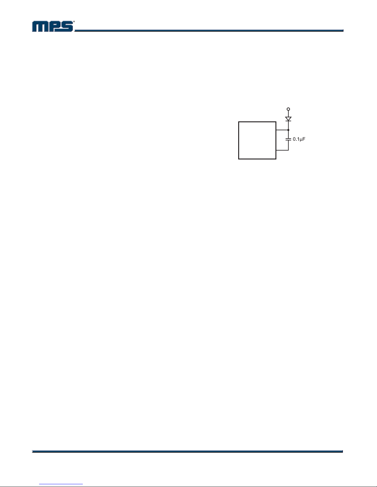
It is recommended that an external bootstrap
diode be added when the input voltage is no
greater than 5V or the 5V rail is available in the
system. This helps improve the efficiency of the
regulator. The bootstrap diode can be a low
cost one such as IN4148 or BAT54.
5V
BS
MP1584
SW
Figure 2—External Bootstrap Diode
This diode is also recommended for high duty
cycle operation (when V
V
(<5Vin) applications.
IN
OUT
/V
>65%) or low
IN
At no load or light load, the converter may
operate in pulse skipping mode in order to
maintain the output voltage in regulation. Thus
there is less time to refresh the BS voltage. In
order to have enough gate voltage under such
operating conditions, the difference of V
IN
–V
OUT
should be greater than 3V. For example, if the
V
is set to 3.3V, the VIN needs to be higher
OUT
than 3.3V+3V=6.3V to maintain enough BS
voltage at no load or light load. To meet this
requirement, EN pin can be used to program
the input UVLO voltage to Vout+3V.
MP1584 Rev. 1.0 www.MonolithicPower.com 14
8/8/2011 MPS Proprietary Information. Unauthorized Photocopy and Duplication Prohibited.
© 2011 MPS. All Rights Reserved.
Page 15
TYPICAL APPLICATION CIRCUITS
V
4.5V - 28V
IN
7
VIN
BST
MP1584 – 3A, 1.5MHz, 28V STEP-DOWN CONVERTER
C4
100nF
8
SW
1
D1
V
OUT
1.8V
EN
2
6
EN
FREQ
MP1584
COMP
GND
5
FB
4
3
C3
100pF
C6
NS
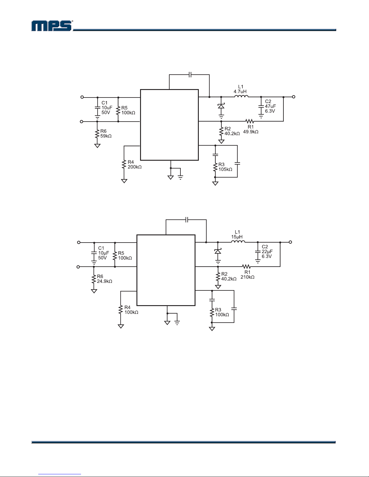
Figure 3—1.8V Output Typical Application Schematic
C4
100nF
8
V
8V - 28V
EN
IN
7
2
6
VIN
EN
FREQ
BST
MP1584
COMP
GND
5
SW
FB
1
D1
4
3
C3
150pF
C6
NS
V
5V
OUT
Figure 4—5V Output Typical Application Schematic
MP1584 Rev. 1.0 www.MonolithicPower.com 15
8/8/2011 MPS Proprietary Information. Unauthorized Photocopy and Duplication Prohibited.
© 2011 MPS. All Rights Reserved.
Page 16
MP1584 – 3A, 1.5MHz, 28V STEP-DOWN CONVERTER
PCB LAYOUT GUIDE
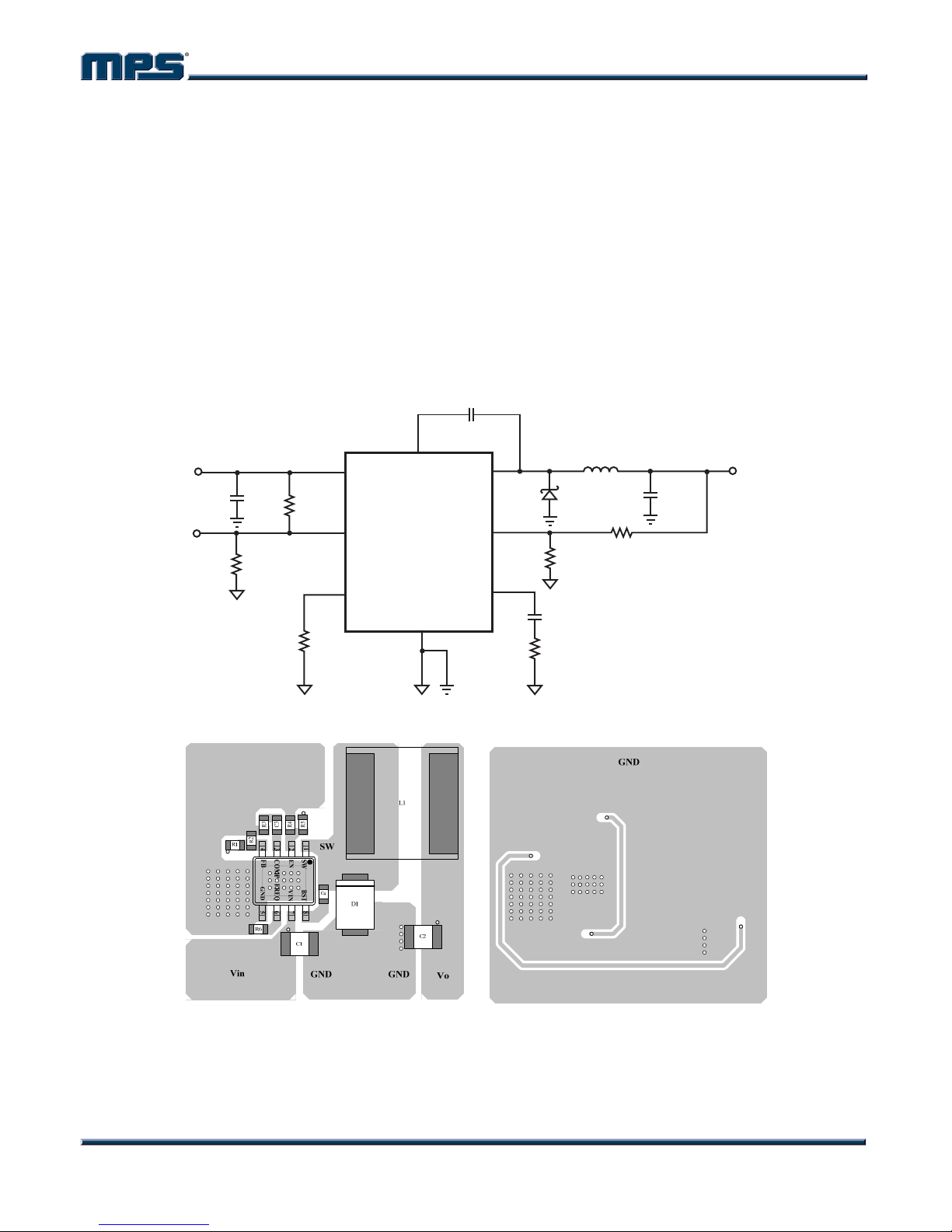
PCB layout is very important to achieve stable
operation. It is highly recommended to duplicate
EVB layout for optimum performance.
If change is necessary, please follow these
guidelines and take Figure 5 for reference.
1) Keep the path of switching current short and
minimize the loop area formed by Input cap,
high-side MOSFET and external switching
diode.
2) Bypass ceramic capacitors are suggested to
be put close to the V
V
IN
EN
C1
R4
Pin.
IN
R5
VIN
EN
BST
MP1584
3) Ensure all feedback connections are short
and direct. Place the feedback resistors and
compensation components as close to the
chip as possible.
4) Route SW away from sensitive analog areas
such as FB.
5) Connect IN, SW, and especially GND
respectively to a large copper area to cool
the chip to improve thermal performance and
long-term reliability.
C4
SW
FB
D1
R2
L1
C2
R1
V
OUT
FREQ
R6
MP1584 Typical Application Circuit
Top Layer
COMP
GND
C3
R3
Bottom Layer
Figure 5MP1584 Typical Application Circuit and PCB Layout Guide
MP1584 Rev. 1.0 www.MonolithicPower.com 16
8/8/2011 MPS Proprietary Information. Unauthorized Photocopy and Duplication Prohibited.
© 2011 MPS. All Rights Reserved.
Page 17
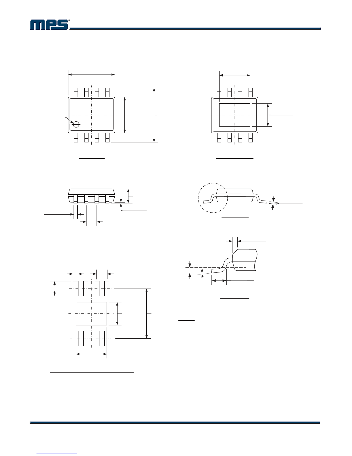
PACKAGE INFORMATION
0.189(4.80)
0.197(5.00)
85
MP1584 – 3A, 1.5MHz, 28V STEP-DOWN CONVERTER
SOIC8E (EXPOSED PAD)
0.124(3.15)
0.136(3.45)
PIN 1 ID
0.013(0.33)
0.020(0.51)
0.024(0.61)
0.063(1.60)
0.150(3.80)
0.157(4.00)
14
TOP VIEW
0.051(1.30)
0.067(1.70)
SEATING PLANE
0.000(0.00)
0.006(0.15)
0.050(1.27)
BSC
FRONT VIEW
0.050(1.27)
0.228(5.80)
0.244(6.20)
BOTTOM VIEW
SEE DETAIL "A"
GAUGE PLANE
0.010(0.25) BSC
o
0o-8
SIDE VIEW
0.016(0.41)
0.050(1.27)
DETAIL "A"
0.010(0.25)
0.020(0.50)
0.089(2.26)
0.101(2.56)
0.0075(0.19)
0.0098(0.25)
o
x 45
0.138(3.51)
RECOMMENDED LAND PATTERN
NOTICE: The information in this document is subject to change without notice. Users should warrant and guarantee that third
party Intellectual Property rights are not infringed upon when integrating MPS products into any application. MPS will not
assume any legal responsibility for any said applications.
MP1584 Rev. 1.0 www.MonolithicPower.com 17
8/8/2011 MPS Proprietary Information. Unauthorized Photocopy and Duplication Prohibited.
© 2011 MPS. All Rights Reserved.
0.103(2.62)
0.213(5.40)
NOTE:
1) CONTROL DIMENSION IS IN INCHES. DIMENSION IN
BRACKET IS IN MILLIMETERS.
2) PACKAGE LENGTH DOES NOT INCLUDE MOLD FLASH,
PROTRUSIONS OR GATE BURRS.
3) PACKAGE WIDTH DOES NOT INCLUDE INTERLEAD FLASH
OR PROTRUSIONS.
4) LEAD COPLANARITY (BOTTOM OF LEADS AFTER FORMING)
SHALL BE 0.004" INCHES MAX.
5) DRAWING CONFORMS TO JEDEC MS-012, VARIATION BA.
6) DRAWING IS NOT TO SCALE.
 Loading...