

Page 1
EV20045DQ-00A
Low Noise, High PSRR, 1A
Linear Regulator EV Board
EV20045DQ-00A Rev. 1.0 www.MonolithicPower.com 1
5/2/2018 MPS Proprietary Information. Unauthorized Photocopy and Duplication Prohibited.
© 2018 MPS. All Rights Reserved.
DESCRIPTION
The EV20045DQ-00A evaluation board
demonstrates the performance of MP20045, a
low noise, low dropout and high PSRR linear
regulator. It operates from a 2.5V to 5.5V input
voltage and the output voltage can be set
externally which ranges from 1.5V to 5V.
The EV20045DQ-00A can supply up to 1A of
load current, and features current limiting, over
temperature protection and power-good status.
An internal PMOS pass element is used to
allow a low 110uA ground current, marking the
MP20045 suitable for battery-power devices.
ELECTRICAL SPECIFICATIONS
Parameter
Symbol
Value
Units
Input Voltage
VIN
3.5 – 5.5
V
Output Voltage
V
OUT
3
V
Load Current
I
OUT
1
A
FEATURES
Up to 1A Output Current
Low 140mV Dropout at 1A
Adjustable Output
56dB PSRR at 1kHz
13μVRMS Low Noise Output
Open Drain Power-Good Status Output
Very Fast Transient Responses
Current Limit and Thermal Protection
APPLICATIONS
Notebook Computers
Cordless Telephones
Cellular Phones
Modems
Hand-Held Instruments
PDA and Palmtop Computers
MPS” and “The Future of Analog IC Technology” are Registered Trademarks of
Monolithic Power Systems, Inc.
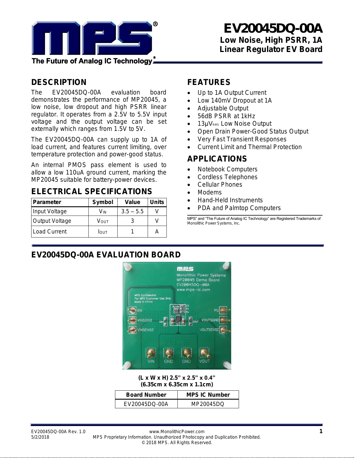
EV20045DQ-00A EVALUATION BOARD
(L x W x H) 2.5” x 2.5” x 0.4”
(6.35cm x 6.35cm x 1.1cm)
Board Number
MPS IC Number
EV20045DQ-00A
MP20045DQ
Page 2
EV20045DQ-00A – LOW NOISE, HIGH PSRR, 1A LINE REGULATOR
EV20045DQ-00A Rev. 1.0 www.MonolithicPower.com 2
5/2/2018 MPS Proprietary Information. Unauthorized Photocopy and Duplication Prohibited.
© 2018 MPS. All Rights Reserved.
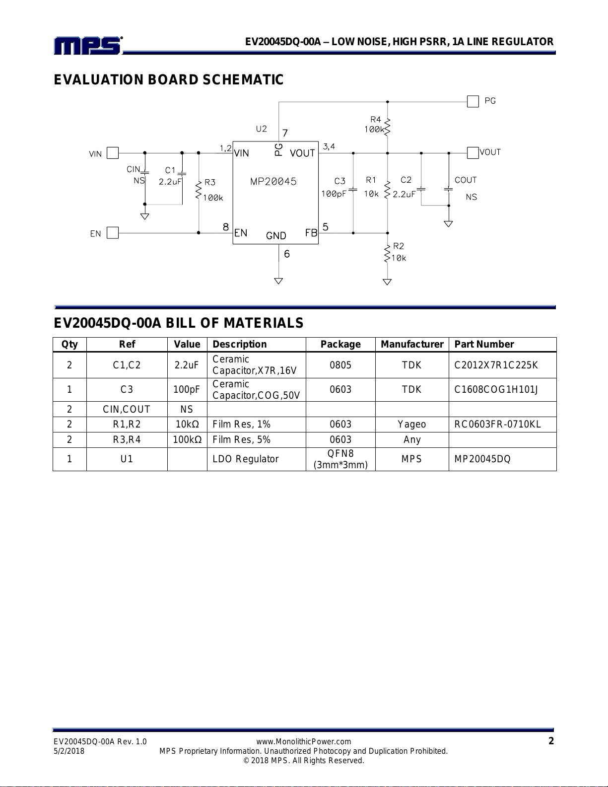
EVALUATION BOARD SCHEMATIC
EV20045DQ-00A BILL OF MATERIALS
Qty
Ref
Value
Description
Package
Manufacturer
Part Number
2
C1,C2
2.2uF
Ceramic
Capacitor,X7R,16V
0805
TDK
C2012X7R1C225K
1
C3
100pF
Ceramic
Capacitor,COG,50V
0603
TDK
C1608COG1H101J
2
CIN,COUT
NS
2
R1,R2
10kΩ
Film Res, 1%
0603
Yageo
RC0603FR-0710KL
2
R3,R4
100kΩ
Film Res, 5%
0603
Any
1
U1
LDO Regulator
QFN8
(3mm*3mm)
MPS
MP20045DQ
Page 3
EV20045DQ-00A – LOW NOISE, HIGH PSRR, 1A LINE REGULATOR
EV20045DQ-00A Rev. 1.0 www.MonolithicPower.com 3
5/2/2018 MPS Proprietary Information. Unauthorized Photocopy and Duplication Prohibited.
© 2018 MPS. All Rights Reserved.
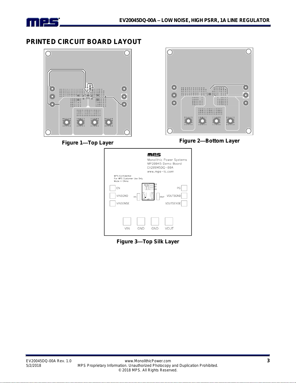
PRINTED CIRCUIT BOARD LAYOUT
Figure 1—Top Layer
Figure 2—Bottom Layer
Figure 3—Top Silk Layer
Page 4
EV20045DQ-00A – LOW NOISE, HIGH PSRR, 1A LINE REGULATOR
EV20045DQ-00A Rev. 1.0 www.MonolithicPower.com 4
5/2/2018 MPS Proprietary Information. Unauthorized Photocopy and Duplication Prohibited.
© 2018 MPS. All Rights Reserved.
QUICK START GUIDE (ADJUSTABLE OUTPUT)
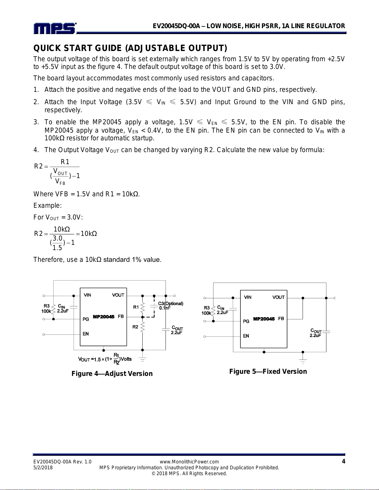
The output voltage of this board is set externally which ranges from 1.5V to 5V by operating from +2.5V
to +5.5V input as the figure 4. The default output voltage of this board is set to 3.0V.
The board layout accommodates most commonly used resistors and capacitors.
1. Attach the positive and negative ends of the load to the VOUT and GND pins, respectively.
2. Attach the Input Voltage (3.5V ≤ VIN ≤ 5.5V) and Input Ground to the VIN and GND pins,
respectively.
3. To enable the MP20045 apply a voltage, 1.5V ≤ VEN ≤ 5.5V, to the EN pin. To disable the
MP20045 apply a voltage, VEN < 0.4V, to the EN pin. The EN pin can be connected to VIN with a
100kΩ resistor for automatic startup.
4. The Output Voltage V
OUT
can be changed by varying R2. Calculate the new value by formula:
1)
V
V
(
R1
R2
FB
OUT
Where VFB = 1.5V and R1 = 10kΩ.
Example:
For V
OUT
= 3.0V:
10kΩ
1)
1.5
3.0
(
10kΩ
R2
Therefore, use a 10kΩ standard 1% value.
Figure 4—Adjust Version
Figure 5—Fixed Version
Page 5
EV20045DQ-00A – LOW NOISE, HIGH PSRR, 1A LINE REGULATOR
NOTICE: The information in this document is subject to change without notice. Please contact MPS for current specifications.
Users should warrant and guarantee that third party Intellectual Property rights are not infringed upon when integrating MPS
products into any application. MPS will not assume any legal responsibility for any said applications.
EV20045DQ-00A Rev. 1.0 www.MonolithicPower.com 5
5/2/2018 MPS Proprietary Information. Unauthorized Photocopy and Duplication Prohibited.
© 2018 MPS. All Rights Reserved.
QUICK START GUIDE (MODIFICATION FOR FIXED OUTPUT)
For modifying the EV20045DQ-00A to accommodate a fixed output voltage version of the MP20045 as
the figure 5:
1. Carefully remove the IC(U1) and replace it with the corresponding fixed output version of the
MP20045 chip.
2. Remove both R1 and R2.
3. Short R1 while leaving R2 open.
4. Attach the positive and negative ends of the load to the VOUT and GND pins, respectively.
5. Attach the Input Voltage (3.5V ≤ VIN ≤ 5.5V) and Input Ground to the VIN and GND pins,
respectively.
6. To enable the MP20045 apply a voltage, 1.5V ≤ VEN ≤ 5.5V, to the EN pin. To disable the
MP20045 apply a voltage, VEN < 0.4V, to the EN pin. The EN pin can be connected to VIN with a
100kΩ resistor for automatic startup.
Please refer to the datasheet for the detailed information of the different output voltage option of
MP20045.
 Loading...