

MPL MIP470 User Manual
MEH-10121-001
MIP470 Preleminary
USERS MANUAL
MPL Industrial PC with Freescale PowerPC™ Processor
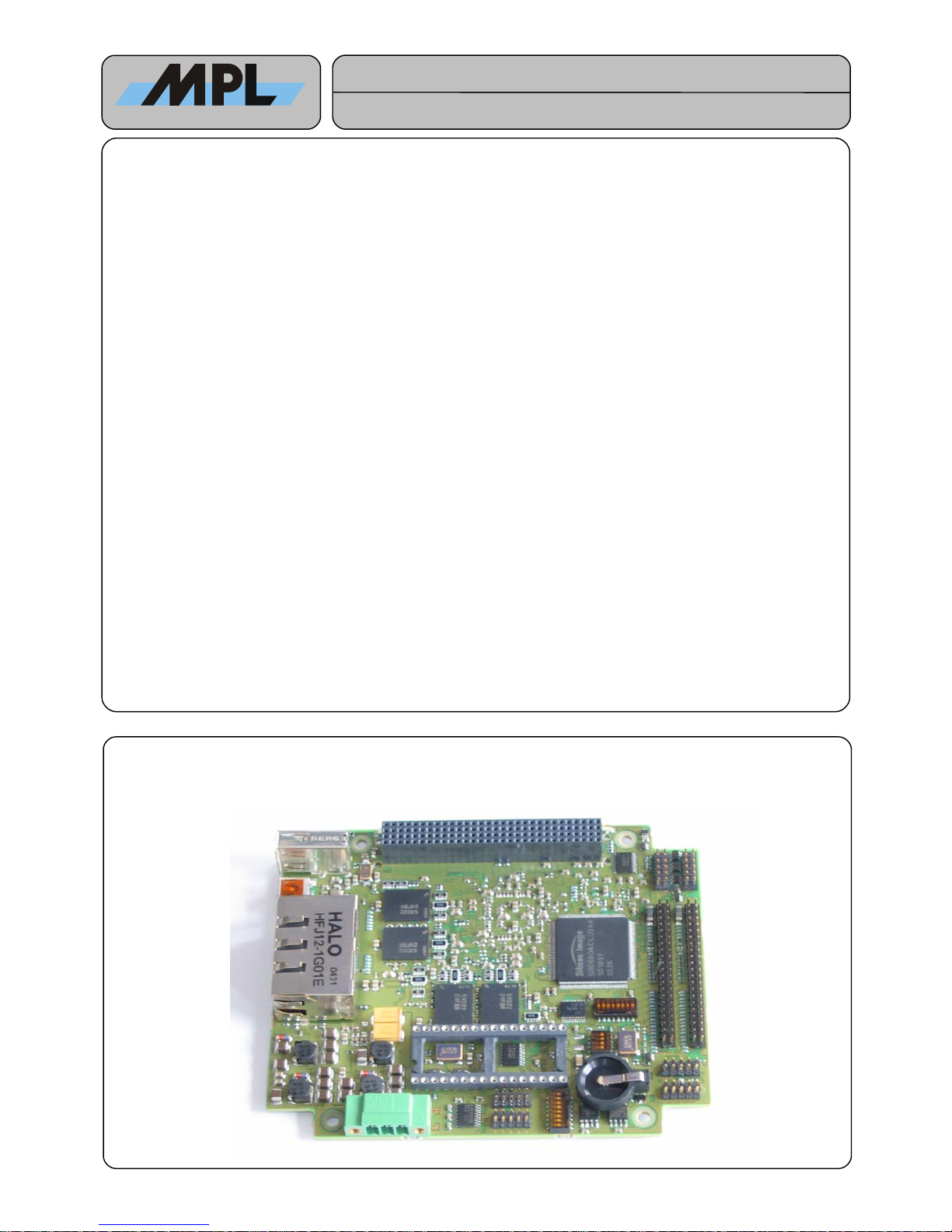
The MIP470 is a highly integrated industrial single board computer in PC/104 form factor. Build around the
MPC8347 Freescale PowerPC™ Processor it is well suited for applications requiring small size, high
performance and Low Power. The MIP470 can be used in a standard operating environment without the
necessity of a fan.
All major components required to build a industrial PC system are implemented on a single PC/104 sized
board. It features two E-IDE, two 10/100/1000Base TX Ethernet, two USB Ports, four serial ports, and a real
time clock. The PC/104+ (PCI) interface offers easy and flexible expansion capabilities.
Integration of the MIP470 into a system is facilitated by the fact of offering standard connectors E-IDE (44
pin header) and LAN (RJ45). The serial interfaces can be accessed through 2mm 10pin headers. Particular
precaution has been taken to the EMC so that an entire system can fulfill the CE and FCC requirements.
The DDR SDRAM is soldered on board and is available with ECC.
All these features make the MIP470 to the ideal solution for any low-cost embedded control application
where a flexible industrial PC is needed.
Features
● Low Power Freescale MPC8347 CPU with
FPU
● Processor clock up to 400 MHz
● Up to 512MByte ECC DDR SDRAM soldered
on board.
● Up to 64MByte Flash on board
● 2 x Integrated 10/100/1000 Mbit/s Ethernet
Controller
• PC/104 Plus PCI only interface
• 2 x USB 2.0 Ports
• Two EIDE HDD ports
• Four RS232 ports
• Low power consumption
2006 by MPL AG
1
High-Tech • Made in Switzerland
MEH-10121-001
MIP470
USERS MANUAL
TABLE OF CONTENTS
1. INTRODUCTION.............................................................................................................................................................. 3
1.1 About this manual........................................................................................................................................................ 3
1.2 MIP470 Variants.......................................................................................................................................................... 3
1.3 Safety precautions and handling................................................................................................................................. 3
1.4 Electrostatic discharge (ESD) protection..................................................................................................................... 3
1.5 Equipment safety......................................................................................................................................................... 3
2. GENERAL INFORMATION AND SPECIFICATIONS...................................................................................................... 4
2.1 Specifications.............................................................................................................................................................. 4
2.1.1 Electrical................................................................................................................................................................ 4
2.1.2 Physical / Power.................................................................................................................................................... 6
2.1.3 Environment.......................................................................................................................................................... 6
2.2 Dimensions ................................................................................................................................................................. 7
3. PREPARATION FOR USE............................................................................................................................................... 8
3.1 Parts Location............................................................................................................................................................. 8
3.2 Switch settings............................................................................................................................................................ 8
3.2.1 S1 User Switch – Software configuration Switch...................................................................................................8
3.2.2 S2 System Switch – Hardware Configuration Switch............................................................................................ 9
3.2.3 S3 System Switch – Hardware configuration Switch............................................................................................. 9
3.3 Indicators................................................................................................................................................................... 10
3.4 Connectors................................................................................................................................................................ 10
3.4.1 J1 USB Host connector....................................................................................................................................... 10
3.4.2 J2 USB OTG connector....................................................................................................................................... 10
3.4.3 J3-1 & J3-2 Ethernet connectors......................................................................................................................... 11
3.4.4 J4- Power Connector........................................................................................................................................... 11
3.4.4.1 Connecting an external Reset Switch............................................................................................................ 11
3.4.5 J5 PC104 PCI Connector.................................................................................................................................... 12
3.4.6 J6 Serial 0............................................................................................................................................................ 12
3.4.7 J7 Serial 1............................................................................................................................................................ 13
3.4.8 J8 Debug............................................................................................................................................................. 13
3.4.9 J9 Factory only.................................................................................................................................................... 13
3.4.10 J10 Secondary IDE Connector.......................................................................................................................... 14
3.4.11 J11 Serial 2........................................................................................................................................................ 14
3.4.12 J12 Serial 3........................................................................................................................................................ 15
3.4.13 J13 Primary IDE Connector............................................................................................................................... 16
3.5 BT1 Battery............................................................................................................................................................... 16
3.6 U4 - Multi purpose socket.......................................................................................................................................... 17
3.6.1 Mounting Memory Modules................................................................................................................................. 17
3.6.2 Switch settings for the Multi Purpose Socket...................................................................................................... 17
3.6.3 Required module properties................................................................................................................................ 17
3.6.4 Device types Examples for the Multi Purpose Socket:........................................................................................ 18
3.6.5 External bootloader............................................................................................................................................. 18
4. OPERATION.................................................................................................................................................................. 19
4.1 Block diagram............................................................................................................................................................ 19
4.2 Memory Map............................................................................................................................................................. 20
4.3 Board Peripherals Mapping....................................................................................................................................... 20
4.4 Extension Registers.................................................................................................................................................. 20
4.4.1 PLD Part number................................................................................................................................................. 21
4.4.2 PLD Version........................................................................................................................................................ 21
4.4.3 Board Revision and Configuration Register........................................................................................................ 21
4.4.4 System Register.................................................................................................................................................. 22
4.4.5 Mode Register..................................................................................................................................................... 22
4.4.6 Software Configuration Register.......................................................................................................................... 23
4.4.7 MPS Register...................................................................................................................................................... 23
4.5 Booting...................................................................................................................................................................... 23
2006 by MPL AG
2
MEH-10121-001
MIP470
USERS MANUAL
1. Introduction
1.1 About this manual
This manual assists the installation and initialization procedure by providing all hardware related information necessary
to handle and configure the MIP470.
For all Bootloader related information please refer to the “U-Boot User Manual for MPL SBC (MEH-10082-002)” supplied
by MPL AG or your local MIP470 supplier. The U-Boot User Manual for MPL SBC” is also available on the Internet under
http://www.mpl.ch in PDF format.
The manual is written for technical personnel responsible for integrating the MIP470 into their system.
1.2 MIP470 Variants
Since the MIP470 is available in various population options, the information in this Manual about Memory size, Processor
speed etc. may vary with your MIP470. The table below lists the actual (as of December 2005) variants, for an actual
table please consult http://www.mpl.ch.
Variants CPU DDR SDRAM Flash Temperature Range
MIP470-1 MPC8347/400MHz 512MByte ECC 64MByte 0°C ... 60°C
Table .1 MIP470 Variants
Note: Not all of the variants may be available. Please consult for http://www.mpl.ch available
variants.
1.3 Safety precautions and handling
For personal safety and safe operation of the MIP470, follow all safety procedures described here and in other sections
of the manual.
• Power must be removed from the system before installing (or removing) the MIP470 to prevent the possibility of
personal injury (electrical shock) and/or damage to the product.
• Handle the product carefully, i.e., dropping or mishandling the MIP470 can cause damage to assemblies and
components.
• Do not expose the equipment to moisture.
WARNING
There are no user-serviceable components on the MIP470
1.4 Electrostatic discharge (ESD) protection
Various electrical components within the product are sensitive to static and electrostatic discharge (ESD). Even a nonsensible static discharge can be sufficient to destroy or degrade a component's operation!
1.5 Equipment safety
Great care is taken by MPL that all its products are thoroughly and rigorously tested before leaving the factory to ensure
that they are fully operational and conform to specification. However, no matter how reliable a product, there is always
the remote possibility that a defect may occur. The occurrence of a defect on this device may, under certain conditions,
cause a defect to occur in adjoining and/or connected equipment. It is the user’s responsibility to ensure that adequate
protection for such equipment is incorporated when installing this device. MPL accepts no responsibility whatsoever for
such kind of defects, however caused.
2006 by MPL AG
3

MEH-10121-001
MIP470
USERS MANUAL
2. General information and specifications
This chapter provides a general overview over the MIP470 and its features. It outlines the electrical and physical
specifications of the product, its power requirements and a list of related publications.
2.1 Specifications
2.1.1 Electrical
Processor:
● Freescale MPC8347 PowerPC™ 32Bit RISC Processor
● High-performance, superscalar processor core
● Floating-point, integer, load/store, system register, and branch processing units
● Eight-way set-associative instruction (32-Kbyte) and data (32-Kbyte) cache
● Low power consumption
Bootloader ROM:
● Up to 64MB Flash EEPROM (population Option)
● 512kB U-Boot (open source) boot loader
● Easy boot loader update
Memory:
● up to 512MByte DDR SDRAM on board
● ECC Support
Multi Purpose Socket:
● Supports different SRAM/FLASH/EPROM, 32 Pin DIL memory components
● Memory sizes up to 2MByte (EPROM)
RTC:
● Backed with onboard battery
● Year 2000 compliant
PC/104-Plus Interface:
● 32 Bit /33MHz PC/104 Plus Interface (PCI Host) up to 4 Busmasters
2006 by MPL AG
4
MEH-10121-001
MIP470
USERS MANUAL
USB:
● 2 USB 2.0 ports for serial transfers up to 480Mbit/s
● ESD protected
Serial ports:
● Four serial Ports 16C550 compatible
● Two serial ports with RS232 signaling (serial 0 and serial 1).
● Two serial port with TTL signaling (serial 2 and serial3)
● Standard transfer rates up to 460 kBaud
● Optional transfer rates up to 1.15 MBaud
● 2 ports with full modem handshake (serial 2 and serial 3)
● Available on four 10pin 2mm headers
E-IDE ports:
● 2 separate channels for up to 4 drives
● available on 44 pin header, 2 mm pitch, for 2,5” Notebook hard disk.
● PIO Mode 4 and Bus Master IDE, transfers up to 16.7 Mbytes/s
● Ultra DMA/33 mode, synchronous DMA mode transfers up to 33 Mbytes/s
● Activity indicator on board
Ethernet:
● 2 x Freescale integrated 10/100/1000 MBit/s Ethernet Controller (TSEC)
● IEEE802.3 10BASE-T, 100BASE-TX and 1000Base-T compatible
● IEEE 802.3u Autonegotiation Support
● IEEE 802.3x 100BASE-TX Flow Control support
● MDI crossover
● Indicators for activity and link/speed detection for 10MBit, 100MBit and 1000MBit on board.
● ESD protected
Indicators:
● Power LED (green)
● Reset / Power Fail LED (red)
● Error LED (red)
● HDD activity LED (green)
● LAN LED (green)
● LAN Speed/Link LED (red/green/amber)
● 1 user programmable LED (green)
2006 by MPL AG
5

MEH-10121-001
MIP470
USERS MANUAL
2.1.2 Physical / Power
Form factor:
PC/104, with connectors in defined I/O connectors overhang regions
Length: 95.9 mm (3.775 inches)
Width: 115.6 mm (4.550 inches)
Height: 14.0 mm (0.550 inch) (excluding PC/104 bus connectors)
Weight:
Typical 110g (fully equipped)
Power supply:
Over PC/104 bus interface or through separate 3-pin Mini-Combicon power connector.
Input Power requirement:
+5V: +5VDC ± 5%
Power consumption:
MIP470 @ 400MHz, DDR266, 512Mbyte ECC DDR and 64MByte Flash:
Typical. 1300mA@5V
2.1.3 Environment
Temperature range:
0°C to +60°C (+32°F to +140°F) @ 400 MHz CPU speed without heat sink
extended temperature range available
Relative humidity:
10% ... 90% non condensing
2006 by MPL AG
6
MEH-10121-001
MIP470
USERS MANUAL
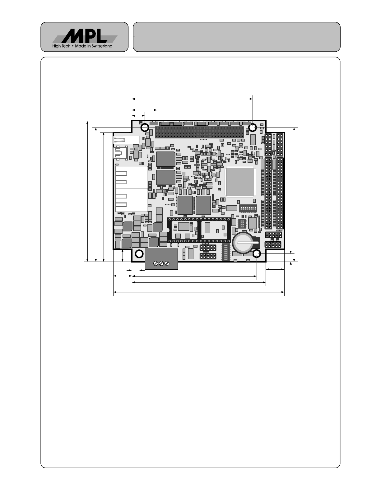
2.2 Dimensions
Drawing not to scale.
Since the MIP470 is implemented as PCI Host, it is not a stack-through board. Please see Chapter tbd for further
information.
2006 by MPL AG
7
Figure 1: Dimensions MIP470
1
O
N
2
3
4
5
6
7
8
1
O
N
2345678
1
O
N
2
3
4
8.3
90.2
85.1
5.1
12.7
12.7
115.6
5.1
87.6
90.8
95.9
90.8
82.5
16.51
8.9
UNITS: mm
MEH-10121-001
MIP470
USERS MANUAL
3.Preparation for use
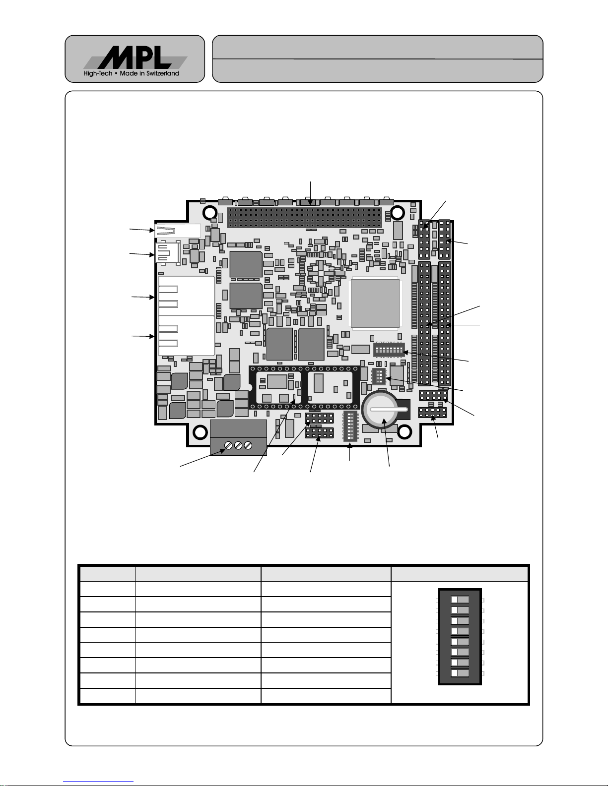
3.1 Parts Location
3.2 Switch settings
3.2.1 S1 User Switch – Software configuration Switch
The Software configuration switch is readable by reading the register EXT_REG.
Switch Off On S1
S1-1 Not yet defined Not yet defined
S1-2 Not yet defined Not yet defined
S1-3 Not yet defined Not yet defined
S1-4 Not yet defined Not yet defined
S1-5 Not yet defined Not yet defined
S1-6 Not yet defined Not yet defined
S1-7 Not yet defined Not yet defined
S1-8 Not yet defined Not yet defined
Table 2: S1 Switch settings
2006 by MPL AG
1
O
N
2
3
4
5
6
7
8
8
Figure 2: Parts Location
1
O
N
2
3
4
5
6
7
8
1
O
N
2345678
1
O
N
2
3
4
J1 USB Host
J2 USB OTG
J3-1 Ethernet 0
J3-2 Ethernet 1
J4 Power
J7 Serial 1
J6 Serial 0
S1 User Switch
BT1 Battery
U4 MPS
J12 Serial A
J11 Serial B
S2 System Switch
S3 System Switch
J13 IDE0
J10 IDE1
J9 factory use only
J8 Debug
J5 PC104 PCI
1
1
1
1
1
1
1
1
A1
1
 Loading...