

查询PC33989DW供应商
MOTOROLA
SEMICONDUCTOR
Freescale Semiconductor, Inc.
TECHNICAL DATA
Advance Information
Order this document by
Rev: 4.91 Date: 10th July, 2002
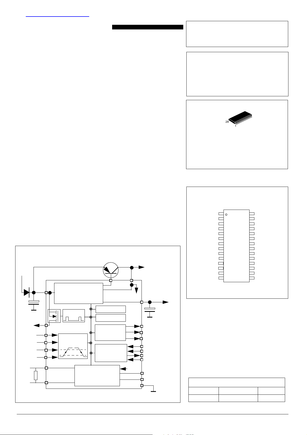
XC33989
System Basis Chip with
High Speed CAN Transceiver
The MC33989 is a monolithic integrated circuit combining many functions
frequently used by automotive ECUs. It incorporates:
- Two voltage regulators.
- Four high voltage inputs.
- 1Mbaud CAN physical interface.
• Vdd1: Low drop voltage regulator, current limitation, over temperature
detection, monitoring and reset function
• Vdd1: Total current capability 200mA.
• V2: Tracking function of Vdd1 regulator. Control circuitry for external bipolar
ballast transistor for high flexibility in choice of peripheral voltage and current
supply.
• Four operational modes (normal, stand-by, stop and sleep mode)
nc...
I
• Low stand-by current consumption in stop and sleep modes
• High speed 1MBaud CAN physical interface.
• Four external high voltage wake-up inputs, associated with HS1 Vbat switch
• 150mA output current capability for HS1 Vbat switch allowing drive of external
switches pull up resistors or relays
• Vsup failure detection
• Nominal DC operating voltage from 5.5 to 27V, extended range down to 4.5V.
• 40V maximum transient voltage
• Programmable software time out and window watchdog
• Safe mode with separate outputs for Watchdog time out and Reset
• Wake up capabilities (four wake up inputs, programmable cyclic sense,
forced wake up, CAN interface, SPI and stop mode over current)
• Interface with MCU through SPI
Simplified Block Diagram
cale Semiconductor,
Frees
Vbat
Vsup
V2CTRL
Vsup monitor
Dual Voltage Regulator
Vdd1 Monitor
Q1
5V/200mA
V2
CAN
supply
Vdd1
SYSTEM BASIS CHIP
WITH HIGH SPEED CAN
SEMICONDUCTOR
TECHNICAL DATA
DW SUFFIX
PLASTIC PACKAGE
CASE 751-F
(SO-28)
PIN CONNECTIONS
RX
TX
Vdd1
Reset
INTB
GND
GND
GND
GND
V2
V2ctrl
Vsup
HS1
L0
1
2
3
4
5
6
7
8
9
10
11
12
13
14
28
27
26
25
24
23
22
21
20
19
18
17
16
15
WDOGB
CSB
MOSI
MISO
SCLK
GND
GND
GND
GND
CANL
CANH
L3
L2
L1
Mode control
Oscillator
Interrupt
Watchdog
Reset
SPI
CAN
V2
INTB
WDOGB
Reset
MOSI
SCLK
MISO
CSB
TX
RX
Gnd
Rterm
HS1
L0
L1
L2
L3
CAN H
CAN L
HS1 control
Programmable
wake-up input
High Speed 1Mbit/s
Physical Interface
For More Information On This Product,
This document contains information on a product under development. Motorola reserves the right
to change or discontinue this product without notice.
Go to: www.freescale.com
Device
ORDERING INFORMATION
Operating
Temperatur e Range
TA = -40 to 125°CPC33989DW
Motorola,Inc 2002
Package
SO-28
Freescale Semiconductor, Inc.
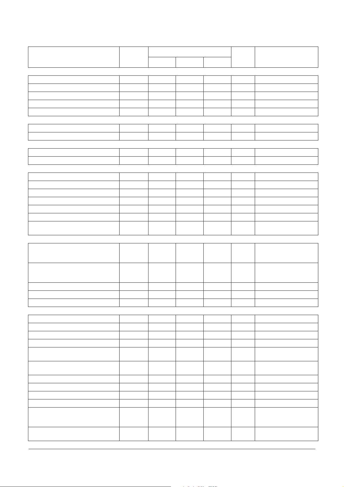
1 MAXIMUM RATINGS
Ratings Symbol Min Typ Max Unit
ELECTRICAL RATINGS
Supply Voltage at Vsup
- Continuous voltage
- Transient voltage (Load dump)
Vsup
Vsup
MC33989
-0.3 27
V
40
nc...
I
cale Semiconductor,
Frees
Logic Inputs (Rx, Tx, MOSI, MISO, CSB, SCLK,
Reset, WDOGB, INTB)
Output current Vdd1 I Internally limited A
HS1
- voltage
- output current
ESD voltage (HBM 100pF, 1.5k)
- HS1, L0, L1, L2, L3
- All other pins
ESD voltage (Machine Model) All pins except
CANH and CANL
L0, L1,L2, L3
- DC Input voltage
- DC Input current
- Transient input voltage (according to ISO7637
specification) and with external component (see figure 1 below).
THERMAL RATINGS
Junction Temperature T
Storage Temperature T
Ambient Temperature (for info only) T
Thermal resistance junction to gnd pins (note 1) Rthj/p 20 °C/W
note 1: gnd pins 6, 7, 8, 9, 20, 21, 22, 23
Figure 1. : Transient test pulse for L0, L1, L2 and L3 inputs
Gnd
Vlog - 0.3 Vdd1+0.3 V
V
I
Vesdh
Vesdm -200 200 V
Vwu DC
j
s
a
1nF
Lx
10 k
-0.3
-4
-2
-0.3
-2
-100
- 40 +150 °C
- 55 +165 °C
- 40 +125 °C
Transient Pulse
Internally limited
Generator
(note)
Gnd
Vsup+0.3 V
40
+100
4
2
2
kV
mA
A
V
V
note: Waveform in accordance to ISO7637 part1, test pulses 1, 2, 3a and 3b.
MC33989 2
For More Information On This Product,
Go to: www.freescale.com
Freescale Semiconductor, Inc.
MC33989
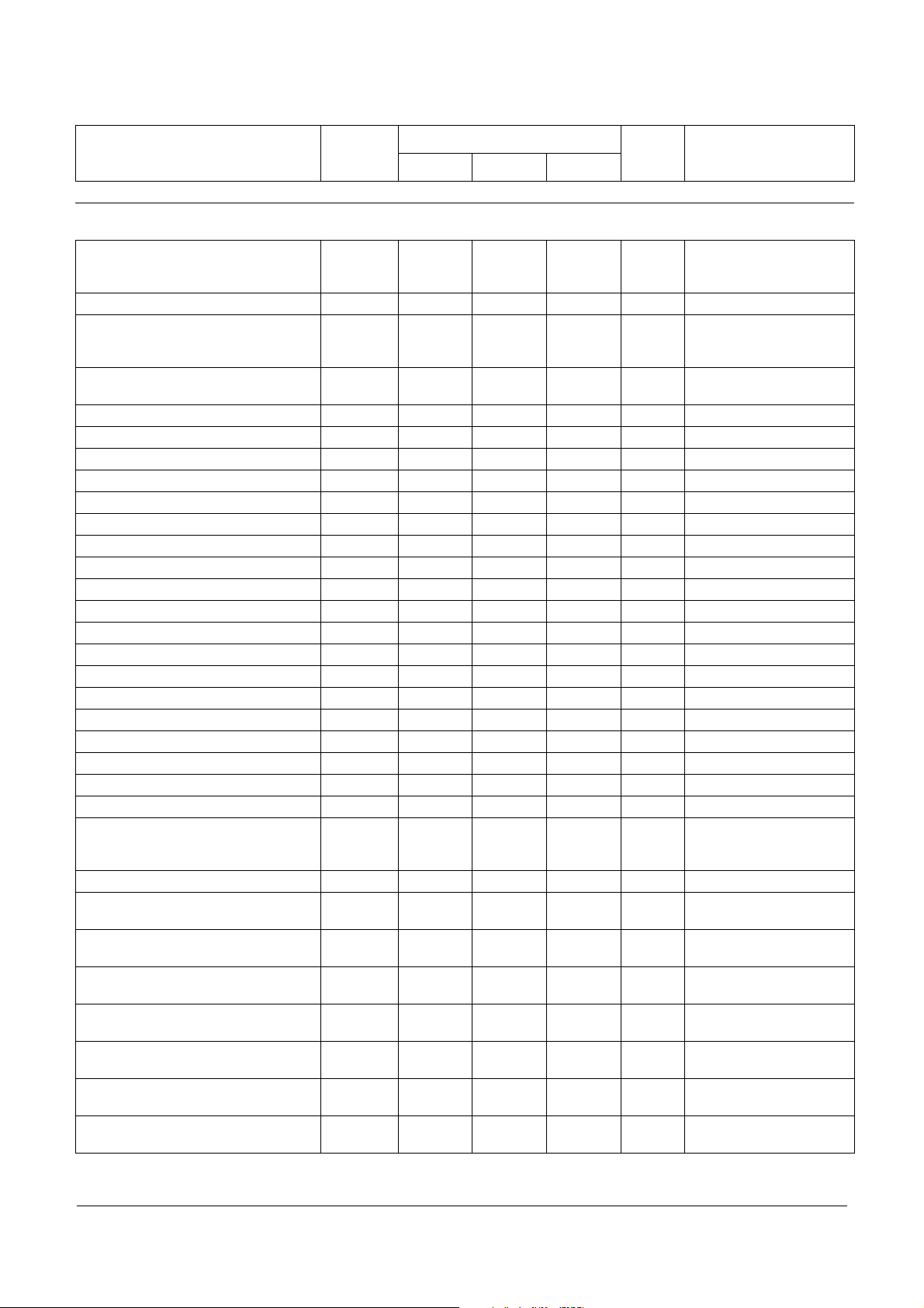
2 ELECTRICAL CHARACTERISTICS
(V
From 5.5V to 18V and Tamb -40°C to 125°C)
sup
For all pins except CANH, CANL, Tx and Rx which are described in the CAN module section
nc...
I
cale Semiconductor,
Frees
Description Symbol
Vsup pin (Device power supply)
Nominal DC Voltage range
Extended DC Voltage range 1 Vsup-ex1 4.5 5.5 V Reduced functionality
Extended DC Voltage range 2 Vsup-ex2 18 27 V (note 3)
Input Voltage during Load Dump
Input Voltage during jump start
Supply Current in Stand-by Mode
(note 2,4) (includes 10mA at Vdd1)
Supply Current in Normal Mode (note 2)
Supply Current in Sleep Mode (note 2,4)
Supply Current in Sleep Mode (note 2,4)
Supply current in sleep mode (note 2,4)
Supply Current in Stop mode (note 2,4)
I out Vdd1 <2mA
Supply Current in Stop mode (note 2,4)
I out Vdd1 <2mA
Supply Current in Stop mode (note 2,4)
Iout Vdd1 < 2mA
BATFAIL Flag internal threshold VBF 1.5 3 4 V
BATFAIL Flag hysteresis VBF hyst 1 V guaranteed by design
Battery fall early warning threshold BFew 5.3 5.8 6.3 V In normal & standby mode
Battery fall early warning hysteresis BFewh 0.1 0.2 0.3 V In normal & standby mode
note 1: Vdd1>4V, reset high, logic pin high level reduced, device is functional.
note 2: Current measured at Vsup pin.
note 3: Device is fully functional. All functions are operating (All mode available and operating, Watchdog, HS1 turn ON turn OFF, CAN cell
operating, L0 to L3 inputs operating, SPI read write operation). Over temperature may occur.
note 4: With CAN cell in sleep-disable state. If CAN cell is sleep-enabled for wake up, an additional 60uA must be added to specified value.
note 5: Oscillator running means “Forced Wake up” or “Cyclic Sense” or “Software Watchdog in stop mode” timer activated. Oscillator not
running means that “Forced Wake up” and “cyclic Sense” and “Software Watchdog in stop mode” are not activated.
Vsup
VsupLD
VsupJS
Isup(stdby)
Isup(norm)
Isup
(sleep1)
Isup
(sleep2)
Isup
(sleep3)
Isup
(stop1)
Isup
(stop2)
Isup
(stop3)
Characteristics
Unit Conditions
Min Typ Max
5.5 18 V
(note 1)
40 V Load dump situation
27 V Jump start situation
12 17 mA Iout at Vdd1 =10mA
CAN recessive or sleep-
disable state
12.5 17 mA Iout at Vdd1 =10mA
CAN recessive or sleep-
disable state
72 105 uA Vdd1 & V2 off, Vsup<12V,
oscillator running (note5)
CAN in sleep-disable state
57 90 uA Vdd1 & V2 off, Vsup<12V
oscillator not running (5)
CAN in sleep-disable state
100 150 uA Vdd1 & V2 off, Vsup>12V
oscillator running (5)
CAN in sleep-disable state
135 210 uA Vdd1 on, Vsup<12V
oscillator running (5)
CAN in sleep-disable state
130 410 uA Vdd1 on, Vsup<12V
oscillator not running (5)
CAN in sleep-disable state
160 230 uA Vdd on, Vsup>12
oscillator running (5)
CAN in sleep-disable state
guaranteed by design
Vdd1 (external 5V output for MCU supply). Idd1 is the total regulator output current. Vdd specification with external capacitor. Stability requirement: C>47uF ESR < 1.3 ohms (tantalum capacitor)
In reset, normal request, normal and standby modes.
Measures with C=47uF Tantalum.
Vdd1 Output Voltage Vdd1out 4.9 5 5.1 V Idd1 from 2 to 200mA
Vdd1 Output Voltage Vdd1out 4 V Idd1 from 2 to 200mA
Tamb -40°C to 125°C
5.5V< Vsup <27V
4.5V< Vsup <5.5V
MC33989 3
For More Information On This Product,
Go to: www.freescale.com
(V
From 5.5V to 18V and Tamb -40°C to 125°C)
sup
For all pins except CANH, CANL, Tx and Rx which are described in the CAN module section
Freescale Semiconductor, Inc.
MC33989
nc...
I
cale Semiconductor,
Frees
Description Symbol
Dropout Voltage Vdd1drop 0.2 0.5 V Idd1 = 200mA
Dropout Voltage, limited output current Vdd1dp2 0.1 0.25 V Idd1 = 50mA
Idd1 output current Idd1 200 285 350 mA Internally limited
Thermal Shutdown (junction) Tsd 160 200
Over temperature pre warning (junction) Tpw 125 160
Temperature Threshold difference Tsd-Tpw 20 40
Reset threshold 1 Rst-th1 4.5 4.6 4.7 V Selectable by SPI. Default
Reset threshold 2 Rst-th2 4.1 4.2 4.3 V Selectable by SPI
Vdd1 range for Reset Active Vdd
Reset Delay Time t
Line Regulation
Line Regulation
Load Regulation
Thermal stability ThermS 30 50 mV
Vdd1 in Stop mode
Vdd1 Output Voltage Vddstop 4.75 5,00 5.25 V Idd1<=2mA
Vdd1 Output Voltage Vddstop2 4.75 5,00 5.25 V Idd1<=10mA
Idd1 stop output current to wake up SBC Idd1s-wu 10 17 25 mA
Idd1 over current wake up deglitcher time Idd1 - dglt 40 55 75 us guaranted by design
Reset threshold Rst-stop1 4.5 4.6 4.7 V
Reset threshold Rst-stop2 4.1 4.2 4.3 V
Line regulation
Load regulation
V2 tracking voltage regulator
note 3: V2 specification with external capacitor
- Stability requirement: C>42uF and ESR<1.3 ohm (tantalum capacitor), external resistor between base and emitter required.
- Measurement conditions: Ballast transistor MJD32C, C=10uF tantalum, 2.2k resistor between base and emitter of ballast transistor.
V2 Output Voltage
I2 output current (for information only) I2 200 mA Depending upon external
V2 ctrl drive current capability I2ctrl 0 10 mA Worst case at Tj=125°C
V2LOW Flag Threshold V2Lth 3.75 4 4.25 V
Logic output pins (MISO) Push pull structure with tri state condition (CSB high).
Low Level Output Voltage Vol 0 1.0 V I out = 1.5mA
High Level Output Voltage Voh Vdd1-0.9 Vdd1 V I out = -250uA
Tristated MISO Leakage Current -2 +2 uA 0V<V
Logic input pins (MOSI, SCLK, CSB)
High Level Input Voltage Vih 0.7Vdd1 Vdd1+0.3
Low Level Input Voltage Vil -0.3 0.3Vdd1 V
High Level Input Current on CSB Iih -100 -20 uA V
Low Level Input Current CSB Iil -100 -20 uA V
MOSI, SCK Input Current Iin -10 10 uA 0<V
(C at Vdd1= 47uF tantal) LR1 5 25 mV 9V<V
(C at Vdd1= 47uF tantal) LR2 10 25 mV 5.5V<V
(C at Vdd1= 47uF tantal) LD 25 75 mV 1mA<I
(C at Vdd1= 47uF tantal) LR-s 5 25 mV 5.5V<V
(C at Vdd1= 47uF tantal) LD-s 15 75 mV 1mA<I
(C at V2 = 10uF tantal) V2 0.99 1 1.01 Vdd1 I2 from 2 to 200mA
r
d
Characteristics
Min Typ Max
1V
430us
Unit Conditions
4.5V< Vsup
°C Normal or standby mode
°C VDDTEMP bit set
°C
value after reset.
Measured at 50% of reset
not tested, guaranted by
charaterization and design
signal
<18, Idd=10mA
sup
<27V, Idd=10mA
sup
<200mA
Idd
Vsup=13.5V, I=100mA
<27V, Idd=2mA
sup
<10mA
Idd
5.5V< Vsup <27V
ballast transistor
<Vdd
miso
=4V
i
=1V
i
<Vdd
IN
MC33989 4
For More Information On This Product,
Go to: www.freescale.com
(V
From 5.5V to 18V and Tamb -40°C to 125°C)
sup
For all pins except CANH, CANL, Tx and Rx which are described in the CAN module section
Freescale Semiconductor, Inc.
MC33989
nc...
I
cale Semiconductor,
Frees
Description Symbol
Reset Pin (output pin only, supply from Vdd1. Structure switch to gnd with pull up current source)
High Level Output current Ioh -300 -250 -150 uA 0<V
Low Level Output Voltage (I
Low Level Output Voltage (I
Reset pull down current Ipdw 2.3 5 mA V>0.9V
Reset Duration after Vdd1 High reset-dur 3 3.4 4 ms
Wdogb output pin (Push pull structure)
Low Level Output Voltage (I
High Level Output Voltage (I
INT Pin( Push pull structure)
Low Level Output Voltage (I
High Level Output Voltage (I
HS1: 150mA High side output pin
Rdson at Tj=25°C, and Iout -150mA Ron25 2 2.5 Ohms Vsup>9V
Rdson at Ta=125°C, and Iout -150mA Ron125 4.5 Ohms Vsup>9V
Rdson at Ta=125°C, and Iout -120mA Ron125-2 3.5 5.5 Ohms 5.5<Vsup<9V
Output current limitation Ilim 160 500 mA
Over temperature Shutdown Ovt 155 190
Leakage current Ileak 10 uA
Output Clamp Voltage at Iout= -10mA Vcl -1.5 -0.3 V no inductive load drive
L0, L1, L2, L3 inputs
Negative Switching Threshold Vthn 2
Positive Switching Threshold Vthp 2.7
Hysteresis Vhyst 0.6 1.3 V 5.5V<Vsup<27
Input current Iin -10 10 uA -0.2V < Vin < 40V
Wake up Filter Time Twuf 8 20 38 us
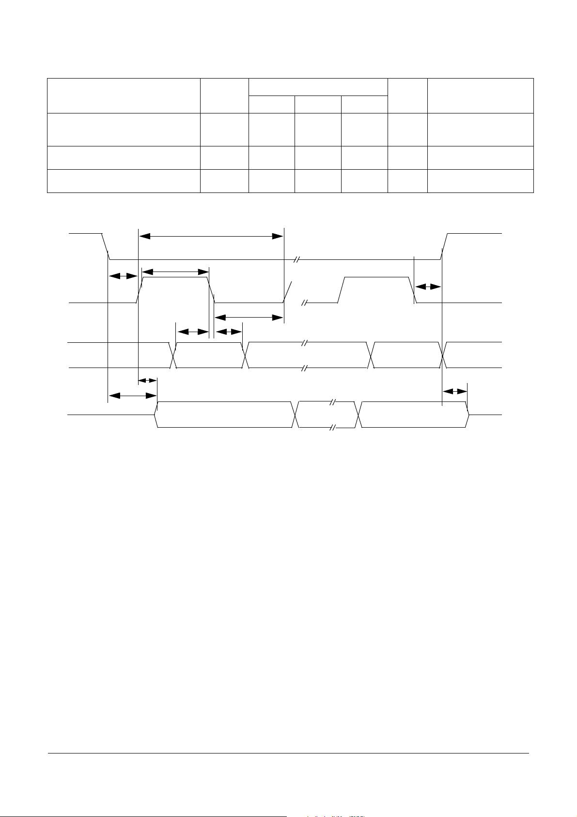
DIGITAL INTERFACE TIMING
SPI operation frequency Freq 0.25 4 MHz
SCLK Clock Period t
SCLK Clock High Time t
SCLK Clock Low Time t
Falling Edge of CS to Rising
Edge of SCLK
Falling Edge of SCLK to Rising Edge of
CS
MOSI to Falling Edge of SCLK t
Falling Edge of SCLK to MOSI t
MISO Rise Time (CL = 220pF) t
MISO Fall Time (CL = 220pF) t
Time from Falling or Rising Edges of CS to:
- MISO Low Impedance
- MISO High Impedance
Time from Rising Edge of SCLK to MISO
Data Valid
=1.5mA) Vol 0 0.9 V 5.5v<V
0
=tbd mA) Vol 0 0.9 V 1v<V
0
=1.5mA) Vol 0 0.9 V 1v<V
0
=-250uA) Voh Vdd1-0.9 Vdd1
0
=1.5mA) Vol 0 0.9 V
0
=-250uA) Voh Vdd1-0.9 Vdd1
0
pCLK
wSCLKH
wSCLKL
t
lead
t
lag
SISU
SIH
rSO
fSO
t
SOEN
t
SODIS
t
valid
Characteristics
Min Typ Max
2.5
2.7
3
3.5
250 N/A ns
125 N/A ns
125 N/A ns
100 N/A ns
100 N/A ns
40 N/A ns
40 N/A ns
2.5
3
3.2
3.3
4
4.2
25 50 ns
25 50 ns
3
3.6
3.7
3.8
4.6
4.7
50
50
50 ns
Unit Conditions
<0.7Vdd
out
<27V
sup
<5.5V
sup
<27V
sup
°C
capability
V 5.5V<Vsup<6V
V 5.5V<Vsup<6V
ns
6V<Vsup<18V
18V<Vsup<27
6V<Vsup<18V
18V<Vsup<27
0.2 V1=<MISO>=0.8V1,
=200pF
C
L
MC33989 5
For More Information On This Product,
Go to: www.freescale.com
(V
From 5.5V to 18V and Tamb -40°C to 125°C)
sup
For all pins except CANH, CANL, Tx and Rx which are described in the CAN module section
Freescale Semiconductor, Inc.
MC33989
nc...
I
cale Semiconductor,
Frees
Description Symbol
STATE MACHINE TIMING
note 1: delay starts at falling edge of clock cycle #8 of the SPI command and start of “Turn on” or “Turn off” of HS1 or V2.
Delay between CSB low to high transistion (at end of SPI stop command) and
Stop mode activation
Interrupt low level duration Tint 7 10 13 us SBC in stop mode
Internal oscillator frequency Osc-f1 100 kHz
Internal low power oscillator frequency Osc-f2 100 kHz
Watchdog period 1 Wd1 8.58 9.75 10.92 ms Normal and standby modes
Watchdog period 2 Wd2 39.6 45 50.4 ms Normal and standby modes
Watchdog period 3 Wd3 88 100 112 ms Normal and standby modes
Watchdog period 4 Wd4 308 350 392 ms Normal and standby modes
Watchdog period accuracy F1acc -12 12 % Normal and standby modes
Normal request mode timeout NRtout 308 350 392 ms Normal request mode
Watchdog period 1 - stop Wd1stop 6.82 9.75 12.7 ms Stop mode
Watchdog period 2- stop Wd2stop 31.5 45 58.5 ms Stop mode
Watchdog period 3 - stop Wd3stop 70 100 130 ms Stop mode
Watchdog period 4 - stop Wd4stop 245 350 455 ms Stop mode
Stop mode watchdog period accuracy F2acc -30 30 % Stop mode
Cyclic sense/FWU timing 1 CSFWU1 3.22 4.6 5.98 ms Sleep and stop modes
Cyclic sense/FWU timing 2 CSFWU2 6.47 9.25 12 ms Sleep and stop modes
Cyclic sense/FWU timing 3 CSFWU3 12.9 18.5 24 ms Sleep and stop modes
Cyclic sense/FWU timing 4 CSFWU4 25.9 37 48.1 ms Sleep and stop modes
Cyclic sense/FWU timing 5 CSFWU5 51.8 74 96.2 ms Sleep and stop modes
Cyclic sense/FWU timing 6 CSFWU6 66.8 95.5 124 ms Sleep and stop modes
Cyclic sense/FWU timing 7 CSFWU7 134 191 248 ms Sleep and stop modes
Cyclic sense/FWU timing 8 CSFWU8 271 388 504 ms Sleep and stop modes
Cyclic sense On time Ton 200 350 500 us in sleep and stop modes
Cyclic sense/FWU timing accuracy Tacc -30 +30 % in sleep and stop mode
Delay between SPI command and HS1
turn on (note 1)
Delay between SPI command and HS1
turn off (note 1)
Delay between SPI and V2 turn on
(note 1)
Delay between SPI and V2 turn off
(note 1)
Delay between Normal Request and Normal mode, after W/D trigger command
Delay between SPI and “CAN normal
mode”
Delay between SPI and “CAN sleep
mode”
Tcsb-stop 18 34 us
Ts-HSon 22 us
Ts-HSoff 22 us
Ts-V2on 9 22 us Standby mode
Ts-V2off 9 22 us Normal modes
Ts-NR2N 15 35 70 us Normal request mode
Ts-CANn 10 us
Ts-CANs 10 us
Characteristics
Unit Conditions
Min Typ Max
Guaranteed by design
detected by V2 off
All modes except Sleep
and Stop, guaranted by
design
Sleep and Stop modes,
guaranted by design
threshold and condition to
be added
Normal or standby mode
Vsup>9V
Normal or standby mode
Vsup>9V
SBC Normal mode
guaranteed by design
SBC Normal mode
guaranteed by design
MC33989 6
For More Information On This Product,
Go to: www.freescale.com
(V
From 5.5V to 18V and Tamb -40°C to 125°C)
sup
For all pins except CANH, CANL, Tx and Rx which are described in the CAN module section
Freescale Semiconductor, Inc.
MC33989
Description Symbol
Delay between CSB wake up (CSB low
to high) and SBC normal request mode
(Vdd1 on & reset high)
Delay between CSB wake up (CSB low
to high) and first accepted SPI command
Delay between INT pulse and 1st SPi
command accepted
CSB
Tlead
nc...
I
SCLK
MOSI
Undefined
Twclkh
Tw-csb 15 40 90 us SBC in stop mode
Tw-spi 90 N/A us SBC in stop mode
Ts-1stspi 20 N/A us In stop mode after wake up
Figure 2. SPI Timing characteristic
Tpclk
Twclkl
Tsi s u
Di 0
Tsi h
Don’t Care
Characteristics
Unit Conditions
Min Typ Max
Tlag
Di 8 Don’t Care
cale Semiconductor,
Frees
Tvalid
Tsoen
MISO
Note:
Incomming data at MOSI pin is sampled by the SBC at SCLK falling edge.
Outcoming data at MISO pin is set by the SBC at SCLK rising edge (after Tvalid delay time).
Do 0
Do 8
Tsodis
MC33989 7
For More Information On This Product,
Go to: www.freescale.com
MC33989
Freescale Semiconductor, Inc.
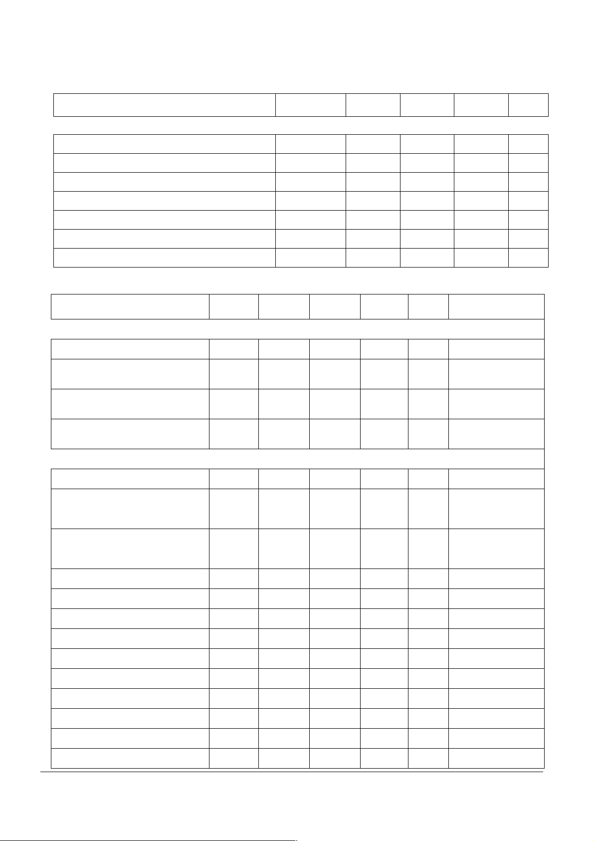
3 CAN MODULE SPECIFICATION
MAXIMUM RATING
Ratings Symbol Min Typ Max Unit
ELECTRICAL RATINGS
CANL,CANH Continuous voltage VcanH,L -27 40 V
CANL,CANH Continuous current IcanH,L 200 mA
CANH, CANL Transient voltage (Load dump, note1) VtrH,L 40 V
CANH, CANL Transient voltage (note2) VtrH,L -40 40 V
Logic Inputs (Tx, Rx) U - 0.5 6 V
ESD voltage (HBM 100pF, 1.5k), CANL, CANH Vesd-ch -4 4 kV
ESD voltage (Machine Model) CANH, CAN L Vesd-cm -200 200 V
V
ELECTRICAL CHARACTERISTICS
= 4,75 to 5,25; V
DD1
=5.5 to 27V; T
sup
= -40 to 125°C unless otherwise specified
amb
nc...
I
cale Semiconductor,
Frees
Descriptions Symbol Min Typ Max Unit Conditions
Supply
Supply current of CAN cell
Supply current of CAN cell
Supply current of CAN cell
CAN in sleep state wake up enable
Supply current of CAN cell
CAN in sleep state wake up disabled
CANH and CANL
Bus pins common mode voltage -27 40 V
Differential input voltage
Differential input voltage 900 mV Common mode
Differential input hysteresis (Rx) 100 mV
Ires
Idom
Isleep
Idis 1 uA V2 regulator off
Vcanh-
Vcanl
1.5 3 mA Recessive state
2 6 mA Dominant state, without
bus load
55 70 uA V2 regulator off
(guaranteed by design)
500 mV Common mode
between -3 and +7V.
Recessive state at Rx
between -3 and +7V.
Dominant state at Rx
Input resistance
Differential input resistance
Unpowered node input current 1.5 mA
CANH output voltage 2.75 4.5 V TX dominant state
CANL output voltage 0.5 2.25 V Tx dominant state
Differential output voltage 1.5 3 V Tx dominant state
CANH output voltage 3 V Tx recessive state
CANL output voltage 2 V Tx recessive state
Differential output voltage 100 mV Tx recessive state
Rin
Rind
5 100 Kohms
10 100 Kohms
8 MC33989
For More Information On This Product,
Go to: www.freescale.com

Freescale Semiconductor, Inc.
Descriptions Symbol Min Typ Max Unit Conditions
CAN H output current capability Icanh -35 mA Dominant state
CAN L output current capability Icanl 35 mA Dominant state
MC33989
DEVICE DESCRIPTION
nc...
I
cale Semiconductor,
Frees
Over temperature shutdown Tshut 160 180°C
CAN L over current detection Icanl-oc 60 200 mA Error reported in CANR
CAN H over current detection Icanh-oc -200 -60 mA Error reported in CANR
TX and RX
Tx Input High Voltage Vih 0.7 Vdd Vdd+0.4 V
Tx Input Low Voltage Vilp -0.4 0.3 Vdd V
Tx High Level Input Current, Vtx=Vdd Iih -10 10 uA
Tx Low Level Input Current, Vtx=0V Iil -100 -50 -20 uA
Rx Output Voltage High, Irx=-250uA Voh Vdd-1 V
Rx Output Voltage Low, Irx=+1mA Vol 0.5 V
Timing
Dominant State Timeout Tdout 200 360 520 us
Propagation loop delay Tx to Rx,
Recessif to dominant
Propagation delay Tx to CAN
Propagation delay CAN to Rx, recessif to
dominant
Propagation loop delay Tx to Rx,
Dominat to recessif
Propagation delay Tx to CAN
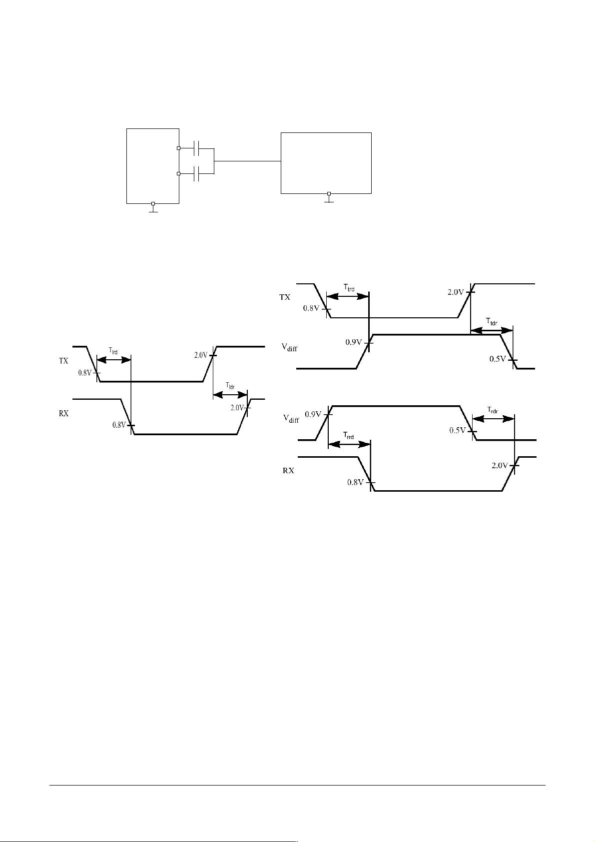
Tlrd 70
80
100
110
Ttrd 20
40
60
100
Trrd 30 80 140 ns
Tldr 70
90
100
130
Ttdr 60
65
75
90
140
155
180
220
65
80
120
160
120
135
160
200
110
120
150
190
210
225
255
310
110
150
200
300
170
180
220
260
130
150
200
300
°C
register
register
ns slew rate 3
slew rate 2
slew rate 1
slew rate 0
ns slew rate 3
slew rate 2
slew rate 1
slew rate 0
ns slew rate 3
slew rate 2
slew rate 1
slew rate 0
ns slew rate 3
slew rate 2
slew rate 1
slew rate 0
Propagation delay CAN to Rx, dominant
to recessif
Non differential slew rate (CanL or CanH)
note 1: Load dump test according to ISO7637 part 1
note 2: Transient test according to ISO7637 part 1, pulses 1,2,3a and 3b, according to schematic figure below.
note 3: Human Body Model; C=100pF, R=1.5Kohms
note 4: Machine Model; C=200pF, R=25ohms
Trdr 20 40 60 ns
Tsl 3
Tsl 2
Tsl 1
Tsl 0
4
3
2
1
19
13.5
8
5
40
20
15
10
V/us slew rate 3
slew rate 2
slew rate 1
slew rate 0
MC33989 9
For More Information On This Product,
Go to: www.freescale.com
Freescale Semiconductor, Inc.
Figure 3. Transient test pulses for CANH and CANL
1nF
CAN H
CAN L
Gnd
note: Waveform in accordance to ISO7637 part1, test pulses 1, 2, 3a and 3b.
nc...
I
1nF
Figure 4. Transceiver AC characteristics
MC33989
DEVICE DESCRIPTION
Transient Pulse
Generator
(note)
Gnd
cale Semiconductor,
Frees
3.1 CAN error detection and wake up
The error and the wake up are reported in the CANR register.
3.1.1 Dominant State Time-out
This protection is based on the fact that all CAN signals can not have more than five bits in a row with the same state. In case
of a condition the Tx pin is stuck at 0v, the transceiver would hold the bus in dominant state making it impossible to the others
CAN modules to use the bus. The protection acts releasing the bus when a dominant signal with more than 350uS typical (
time)
is present in the Tx signal. After entering the fault condition the driver is disabled. To clear this disabled state the CAN
transceiver needs to have its input going to recessive state.
3.1.2 Internal Error output flags
There are internal error flags to signals when one of the below condition happens. The errors are reported in CAN register.
• Thermal protection activated (bit THERM)
• Over Current detection in CANL or CANH pins (bit CUR).
• Time-out condition for dominant state (bit TXF).
3.1.3 Sleep mode & Wake-up via CAN bus feature
The HSCAN interface enters in a low consumption mode when the “CAN sleep mode” is enabled. In this mode the HSCAN
module will have a 60uA consumption via internal 5V.
When in sleep mode the transmitter and the receiver are disabled, the only part of circuit which remains working is the wake
up module which contains a special low power receiver to check the bus lines and according to its activity generate a wake up
output signal. The conditions for the wake is meet when there are 3 valid pulses in a row. A valid signal must have a pulse width
bigger than 0.5us and no more than 0.5ms.
Tdout
MC33989 10
For More Information On This Product,
Go to: www.freescale.com

Freescale Semiconductor, Inc.
The block diagram illustrates how the wake up signal is generated. First the CAN signal is detected by a low consumption
receiver (WU receiver). Then the signal passes through a pulse width filter which discards the undesired pulses. The pulse must
have a width bigger than 0.5us and smaller than 500us to be acepted. When a pulse is discarded the pulse counter is reseted
nc...
I
and no wake signal is generated, otherwise when a pulse is acepted the pulse counter is incremented and after three pulses the
wake signal is asserted.
Each one of the pulses must be spaced by no more than 500us. In that case the pulse counter is reset and no wake signal is
generated. This is accomplished by the wake time-out generator. The wake up cycle is completed (and the wake flag reset)
when the CAN interface is brought to “CAN normal” mode.
The wake up capability of the CAN can be disabled, refer to SPI interface and register section, CAN register.
Figure 5. Wake up block diagram
MC33989
diagram to be inserted
cale Semiconductor,
Frees
MC33989 11
For More Information On This Product,
Go to: www.freescale.com

MC33989
Freescale Semiconductor, Inc.
4 GENERAL DESCRIPTION
The MC33989 is an integrated circuit dedicated to automotive applications. It includes the following functions:
- One full protected voltage regulator with 200mA total output current capability available at Vdd1 external pin.
- Driver for external path transistor for V2 regulator function.
- Reset, programmable watchdog function, INT, 4 operational modes
- Programmable wake up input and cyclic sense wake up
- Can high speed physical interface
4.1 Device Supply
The device is supplied from the battery line through the Vsup pin. An external diode is required to protect against negative
transients and reverse battery. It can operate from 4.5V and under the jump start condition at 27V DC. This pin sustains standard
automotive voltage conditions such as load dump at 40V. When Vsup falls below 3V typical the MC33989 detects it and store the
information into the SPI register, in a bit called “BATFAIL”. This detection is available in all operation modes.
The device incorporates a battery early warning function, which provides a maskable interrupt when the Vsup voltage is below
6V typical. An hysteresis is included. Operation is only in Normal and Standby modes. Vsup low is reported in IOR register.
4.2 Vdd1 Voltage Regulator
Vdd1 Regulator is a 5V output voltage with output current capability up to 200mA. It includes a voltage monitoring circuitry
associated with a reset function. The Vdd1 regulator is fully protected against over current, short-circuit and has over temperature
detection warning flags (bit VDDTEMP in MCR and INTR registers) and over temperature shutdown with hysteresis.
4.3 V2 regulator
V2 Regulator circuitry is designed to drive an external path transistor in order to increase output current flexibility. Two pins are
nc...
I
used: V2 and V2 ctrl. Output voltage is 5V and is realized by a tracking function of the Vdd1 regulator. Recommended ballast
transistor is MJD32C. Other transistor can be used, however depending upon the PNP gain an external resistor-capacitor
network might be connected. V2 is the supply input for the CAN cell. The state of V2 is reported in the IOR register (bit V2LOW set
to 1 if V2 is below 4.5V typical).
cale Semiconductor,
Frees
4.4 HS1 Vbat Switch Output
HS1 output is a 2 ohms typical switch from Vsup pin. It allows the supply of external switches and their associated pull up or
pull down circuitry, in conjunction with the wake up input pins for example. Output current is limited to 200mA and HS1 is
protected against short-circuit and has an over temperature shutdown (bit HS1OT in IOR and bit HS1OT-V2LOW in INTR
register). HS1 output is controlled from the internal register and SPI. It can be activated at regular intervals in sleep and stop
modes thanks to internal timer. It can also be permanently turned on in normal or stand-by modes to drive loads or supply
peripheral components. No internal clamping protection circuit is implemented, thus dedicated external protection circuit is
required in case of inductive load drive.
4.5 Battery fall early warning:
Refer to paragraph 4.1.
4.6 Internal Clock
The device has an internal clock used to generate all timings (reset, watchdog, cyclic wake up, filtering time etc....). Two
oscillators are implemented. A high accuracy (+-12%) used in Normal request, normal and standby modes and a low accuracy (+30%)used in sleep and stop modes.
4.7 Functional Modes
The device has four modes of operation, the stand-by mode, normal mode, stop and sleep modes. All modes are controlled by
the SPI. An additional temporary mode called “normal request mode” is automatically accessed by the device after reset or wake
up from stop mode. A reset mode is also implemented. Special modes and configuration are possible for debug and program
MCU flash memory.
4.7.1 Reset mode:
In this mode, reset pin is low, an a timer is running for a time “reset-dur”. After this time is ellapsed, the SBC enters Normal
Request mode. Reset mode is enter if a reset condition occurs (Vdd1 low, watchdog timeout or watchdog trigger in closed
window).
4.7.2 Normal request mode:
4.7.2.1 Description:
This is a temporary mode automatically accessed by the device after reset mode or after the SBC wake up from stop mode.
After wake up from sleep mode or after device power up the SBC enters the reset mode first and then enters the Normal request
mode. After a wake up from stop mode, the SBC enters Normal Request mode directly.
In Normal Request mode the Vdd1 regulator is ON, V2 is off, the reset pin is high. As soon as the device enters the normal
request mode an internal 350ms timer is started. During these 350ms the micro controller of the application must addressed the
SBC via SPI and configure the watchdog register. This is the condition for the SBC to stop the 350ms timer and to go into the
Normal mode or standby mode and to set the watchdog timer according to configuration.
12 MC33989
For More Information On This Product,
Go to: www.freescale.com

MC33989
4.7.2.2 Normal request entered and no W/D configuration occurs:
In case the Normal request mode is entered after SBC power up or after a wake up from stop mode, and if no W/D
configuration occurs while the SBC is in Normal request mode, the SBC goes to reset mode after the 350ms time period is
expired, and then goes again into Normal request mode. If no W/D configuration is done, the SBC alternatively goes from normal
request into reset then normal request modes etc.
In case the Normal request mode is entered after a wake up from sleep mode and if no W/D configuration occurs while the
SBC is in Normal request mode, the SBC goes back to sleep mode.
4.7.3 Normal mode:
In this mode both regulators are ON and this corresponds to the normal application operation. All functions are available in
this mode (watchdog, wake up input reading through SPI, HS1 activation, CAN communication). The software watchdog is
running and must be periodically cleared through SPI.
4.7.4 Standby mode:
Only the regulator 1 is ON. Regulator 2 is turned OFF by disabling the V2 ctrl pin. Only the wake-up capability of the CAN
interface is available. Other functions available are: wake up input reading through SPI, HS1 activation. The watchdog is running.
4.7.5 Sleep mode:
Regulators 1 and 2 are OFF. The current from Vsup pin is reduced. In this mode, the device can be awakened internally by
cyclic sense via the wake up inputs pins and HS1 output, from the “forced wake up” function and from the CAN physical interface.
When a wake up occurs the SBC goes first into reset mode, then enters Normal request mode.
4.7.6 Stop mode
nc...
I
4.7.6.1 Description
Regulator 2 is turned OFF by disabling the V2 ctrl pin. The regulator 1 is activated in a special low power mode which allow to
deliver few mA. The objective is to maintain the MCU of the application supplied while it is turned into power saving condition (i.e
stop or wait mode). In stop mode the device supply current from Vbat is very low.
When the application is in stop mode (both MCU and SBC), the application can wake up from the SBC side (ex cyclic sense,
forced wake up, CAN message, wake up inputs and over current on Vdd1) or the MCU side (key wake up etc.).
Stop mode is always selected by SPI. In stop mode the Software watchdog can be “running” or “not running” depending upon
selection by SPI (RCR register, bit WDSTOP). If W/D runs, to clear the W/D the SBC must be wake up by a CSB pin (SPI wake
up). In stop mode, SBC wake up capability are identical as in sleep mode. Refer to table 1.
4.7.6.2 Application wake up from SBC side:
When application is in stop mode, it can wake up from the SBC side. When a wake up is detected by the SBC (ex CAN, Wake
up input etc.) the SBC turns itself into Normal request mode and generates an interrupt pulse at the INTB pin.
4.7.6.3 Application wake up from MCU side:
When application is in stop mode, the wake up event may come from the MCU side. In this case the MCU signals to the SBC
by a low to high transition on the CSB pin. Then the SBC goes into Normal Request mode and generates an interrupt pulse at the
INTB pin.
4.7.6.4 Stop mode current monitor:
cale Semiconductor,
Frees
If the Vdd1 output current exceed an internal threshold (Idd1s-wu), the SBC goes automatically into normal request mode and
generates an interrupt at the INTB pin. The interrupt is not maskable and the interrupt register will have no flag set.
4.7.6.5 INT generation when wake up from stop mode:
When the SBC wakes up from stop mode, it first enters the normal request mode and then generates a pulse (10us typical) on
the INTB pin. These interrupts are not maskable, and the wake up event can be read through the SPI registers (CANWU bit in
RCR register and LCTRx bit in WUR register). In case of wake up from Stop mode over current or from forced wake up, no bit are
set. After the INT pulse the SBC accept SPi command after a time delay (Ts-1stspi parameter).
Freescale Semiconductor, Inc.
4.7.6.6 Software watchdog in stop mode:
If watchdog is enabled, the MCU has to wake up independently of the SBC before the end of the SBC watchdog time. In order
to do this the MCU has to signals the wake up to the SBC through the SPI wake up (CSB activation). Then the SBC wakes up and
jump into the normal request mode. MCU has to configured the SBC to go to either normal or standby mode. The MCU can then
decide to go back again to stop mode.
If no MCU wakes up occurs within the watchdog timing, the SBC will activate the reset pin and jump into the normal request
mode. The MCU can then be initialized.
4.7.6.7 Stop mode enter command:
Stop mode is entered at end of the SPI message at the rising edge fo the CSB . Refer to to ”Tcsb-stop” data in state machine
timing table.
MC33989 13
For More Information On This Product,
Go to: www.freescale.com

MC33989
Once stop mode is entered the SBC could wake up from the V1 regulator over current detection. In order to allow time for the
MCU to complete the last CPU instruction to allow MCU to enter its low power mode, a deglitcher time of typicall 40us is
implemented.
figure below indicate operation to enter stop mode.
SPI Stop / Sleep command
SPI CSB
Freescale Semiconductor, Inc.
nc...
I
cale Semiconductor,
Frees
Tc sb - st o p
SBC in Normal or Standby mode
4.8 Reset and watchdogb pins, sofwtare watchdog operations:
4.8.1 Software watchdog (selectable window or time out watchdog)
Software watchdog is used in the SBC normal and stand-by modes for the MCU monitoring. The watchdog can be either
window or time out. This is selectable by SPI (register TIM1, bit WDW). Default is window watchdog. The period for the watchdog
is selectable from SPI from 10 to 350ms (register TIM1, bits WDT0 and WDT1). When the window watchdog is selected, the
closed window is the first part of the selected period, and the open window is the second part of the period. Refer to SPI TIM
register description. The watchdog can only be cleared within the open window time. An attempt to clear the watchdog in the
closed window will generate a reset. Watchdog is cleared through SPI by addressing the TIM1 register.
4.8.2 Reset pin description
A reset output is available in order to reset the microcontroller. Two operation modes for the reset pin are available, mode 1
and mode 2 (refer to table for reset pin operation).
The reset cause when SBC is in mode 1 are:
- Vdd1 falling out of range: if Vdd1 falls below the reset threshold (parameter
to nominal voltage.
- Power on reset: at device power on or at device wake up from sleep mode, the reset is maintained low until Vdd1 is within its
operation range.
- Watchdog time out: if the watchdog is not cleared the SBC will pull the reset pin low for the duration of the reset duration time
(parameter: reset-dur).
In mode 2, the reset pin is not activated in case of watchdog time out. Refer to” table for reset pin operation“for mode detail.
For debug purposes at 25°C, reset pin can be shorted to 5V, thanks to its internal limited current drive capability.
4.8.3 Reset and Wdogb operation: mode1 and mode 2 (safe mode):
The watchdog and reset functions have two modes of operation: mode 1 and mode 2 (mode 2 is also called safe mode).
These modes are independent of the SBC modes (Normal, stand-by, sleep, stop). Mode 1 or mode 2 selection is done through
SPI (register MCR, bit SAFE). Default mode after reset is mode 1.
Table below is the reset and watchdog output mode of operation. Two modes (mode 1 and mode 2) are available and are
selectable through the SPI, safe bit. Default operation after reset or power up is mode 1.
In both modes reset is active at device power up and wake up.
In mode 1: Reset is activated in case of Vdd1 fall or watchdog not triggered. Wdogb output is active low as soon as reset goes
low and stays low as long as the watchdog is not properly re-activated by SPI.
In mode 2, safe mode: Reset in not activated in case of Watchdog failure. WDOGB output has same behavior as in mode 1.
The Wdogb output pin is a push pull structure than can drive external component of the application in order for instance to signal MCU wrong operation.
Idd1 - dglt
SBC in stop mode
no Idd1 over I wake up
Rst-th), the reset pin is pull low until Vdd1 return
SBC in stop mode
with Idd1over I wake up
Events Mode
Device power up 1 or 2 (safe mode) low to high low to high
- Vdd1 normal
- Watchdog properly triggered
1 high high
WDOGB
output
Reset
output
14 MC33989
For More Information On This Product,
Go to: www.freescale.com

MC33989
Freescale Semiconductor, Inc.
Events Mode
Vdd1 < Rst-th 1 high low
Watchdog time out reached 1 low (note1) low
- Vdd1 normal
- Watchdog properly triggered
Vdd1 < Rst-th 2 (safe mode) high low
Watchdog time out reached 2 (safe mode) low (note1) high
note1: Wdogb stays low until the Watchdog register is properly addressed through SPI.
Figure 6. Reset and Wdogb functions diagram in mode 1 and 2
Vdd1
Reset
nc...
I
4.9 Wake Up capabilities
wake up event is stored into the WUR or CAN registers. The MCU can then access to the wake up source. The wake up options
are selectable trough SPI while the device is in normal or standby mode and prior to go to enter low power mode (sleep or stop
mode). When a wake up occurs from sleep mode the device activates Vdd1. It generates an interrupt if wake up occurs from stop
mode.
4.9.1 Wake up from wake up inputs (L0, L1, L2, L3) without cyclic sense
cale Semiconductor,
modes). The wake up pins are able to handle 40V DC. The internal threshold is 3V typical and these inputs can be used as input
port expander. The wake up inputs state can be read through SPI (register WUR).
level sensitivity, and the LPC register must be configured with 0xx0 data (bit LX2HS1 set at 0 and bit HS1AUTO set at 0).
Frees
configured toghether, L2 and L3 are configured toghether.
MODE 1
MODE 2
Several wake-up capabilities are available for the device when it is in sleep or stop mode. When a wake up has occurred, the
The wake up lines are dedicated to sense external switches state and if changes occur to wake up the MCU (In sleep or stop
In order to select and activate direct wake up from the Lx inputs the WUR register must be configured with the appropriate
Level sensitivity is selected by WUR register. Level sensitivity are configured by pair of Lx inputs: L0 and L1 level sensitvity are
WDOGB
SPI
W/D clear
SPI CSB
Reset
WDOGB
2 (safe mode) high high
Watchdog
period
WDOGB
output
Reset
output
Watchdog time out
Watchdog
register
addressed
4.9.2 Cyclic sense wake up (Cyclic sense timer and wake up inputs L0, L1, L2, L3)
The SBC can wake up upon state change of one of the four wake up input lines (L0, L1, L2 and L3) while the external pull up
or pull down resistor of the switches associated to the wake up input lines are biased with HS1 Vsup switch. The HS1 switch is
activated in sleep or stop mode from an internal timer. Cyclic sense and Forced wake up are exclusive. If Cyclic Sense is enabled
the forced up can not be enabled.
In order to select and activate the cyclic sense wake up from the Lx inputs the WUR register must be configured with the
appropriate level sensitivity, and the LPC register must be configured with 1xx1 data (bit LX2HS1 set at 1 and bit HS1AUTO set at
1). The wake up mode selection (direct or cyclic sense) is valid for all 4 wake up inputs.
4.9.3 Forced wake up
SBC can wake up automatically after a pre determined time spent in sleep or stop mode. Cyclic sense and Forced wake up
are exclusive. If Forced wake up is enabled (FWU bit set to 1 in LPC register) the Cyclic Sense can not be enabled.
4.9.4 CAN interface wake up
The device incorporates a high speed 1MBaud CAN physical interface. Its electrical parameters for the CANL, CANH, Rx
MC33989 15
For More Information On This Product,
Go to: www.freescale.com

MC33989
and Tx pins are compatible to ISO11898 specification (IS0 11898: 1993(E)). The control of the CAN physical interface operation
is done through the SPI. CAN modes are independent of the SBC operation modes.
The device can wake up from a CAN message if CAN wake up has been enabled. Refer to CAN module description for detail
of wake up detection.
4.9.5 SPI wake up
The device can wake up by the CSB pin in sleep or stop mode. Wake up is detected by CSB pin transition from low to high
level. In stop mode this correspond to the condition where MCU and SBC are in Stop mode and when the application wake up
event comes through the MCU.
4.9.6 Device power up, SBC wake up
After device or system power up, or after the SBC wakes up from sleep mode, it enters into “reset mode” then into “normal
request mode”.
4.10 Debug mode: hardware and software debug with the SBC.
When the SBC is mounted on the same printed circuit board as the mico controller it supplies, both application software and
SBC dedicated routine must be debugged. Following features allow the user to debug the software by allowing the possibility to
disable the SBC internal software watchdog timer.
4.10.1 Device power up, reset pin connected to Vdd1
At SBC power up, the Vdd1 voltage is provided, but if no SPI communication occurs to configure the device, a reset occurs
every 350ms. In order to allow software debug and avoid MCU reset the Reset pin can be connected directly to Vdd1 by a jumper.
Freescale Semiconductor, Inc.
nc...
I
cale Semiconductor,
Frees
4.10.2 Debug modes with software watchdog disabled though SPI (Normal Debug, Standby Debug and Stop Debug)
The software watchdog can be disabled through SPI. In order to avoid unwanted watchdog disable and to limit the risk of
disabling the watchdog during SBC normal operation the watchdog disable has to be done with the following sequence:
Step 1) Power down the SBC
Step 2) Power up the SBC (The BATFAIL bit is set, and the SBC enters normal request mode)
Step 3) Write to TIM1 register to allow SBC to enter Normal mode
Step 4) Write to MCR register with data 0000 (this enables the debug mode). (Complete SPI byte: 000 1 0000)
Step 5) Write to MCR register normal debug (0001 x101)
While in debug mode, the SBC can be used without having to clear the W/D on a regular basis to facilitate software and
hardware debug.
Step 6) To leave the debug mode, write 0000 to MCR register.
At step 2, the SBC is in normal request. Step 3, 4 and 5 should be done consecutiveley and withing the 350ms time period of
the normal requets mode. If not, the SBC will go into reset mode and enter again normal request.
When the SBC is in debug mode, and has been set into stop debug or sleep debug, when a wake up occurs the SBC enters
Normal requets mode, for a time period of 350ms. In order to avoid the SBC to generate a reset (enter reset mode) the desired
next debug mode (normal debug or standby debug) should be configured within the 350ms time period of the normal requets
mode (for detail refer to “State machine in debug mode”).
To avoid entering debug mode after a power up, first read BATFAIL bit (MCR read) and write 0000 into MCR.
The graph below illustrates the debug mode enter.
VSup
Vdd1
Batfail
TIM1(step 3)
SPI
MCR(step4)
debug mode
4.10.3 MCU flash programming configuration
In order to allow the possibility to download software into the application memory (MCU EEPROM or Flash) the SBC allows
the following capabilities: The Vdd1 can be forced by an external power supply to 5V and the reset and Wdogb outputs by
external signal sources to zero or 5V and this without damage. This allow for instance to supply the complete application board by
external power supply and to apply the correct signal to reset pins.No function of the SBC are operating.
Due to pass transistor from Vdd1 to Vsup, supplying the device from Vdd1 pin biases the Vsup pin. So Vsup should be left
open of forced to value above 5V. Reset pin is periodically pulled low for “reset dur” time (3.4ms typical) and then pulled to Vdd1
for 350ms typical. During the time reset is low, reset pin sinks 5mA maximum (Ipdw parameter).
MCR (step5)
MCR (step6)
SPI: read batfail
SBC in debug Mode, no W/D
SBC not in debug Mode and W/D on
16 MC33989
For More Information On This Product,
Go to: www.freescale.com

MC33989
Freescale Semiconductor, Inc.
Figure 7. Simplified schematic for Flash programming
Simplified connection used in Flash programming mode
Vsup (open or >5V
SBC MCU = Flash
4.11 Package and thermal consideration
The device is proposed in a standard surface mount SO28 package. In order to improve the thermal performances of the
SO28 package, 8 pins are internally connected to the lead frame and are used for heat transfer to the printed circuit board.
nc...
I
Vdd1
reset
Wdogb
External supply and sources applied to Vdd1, reset
and Wdogb test points on application circuit board.
Programming bus
cale Semiconductor,
Frees
MC33989 17
For More Information On This Product,
Go to: www.freescale.com

MC33989
Freescale Semiconductor, Inc.
5 TABLE OF OPERATION
The table below describes the SBC operation modes. “Normal Debug”, “Standby Debug” and “Stop Debug” are entered via
special sequence described at debug mode paragraph.
nc...
I
cale Semiconductor,
Frees
mode
Normal
Request
Normal
Standby
Stop
Sleep
Debug
Normal
Debug
Standby
Stop
Debug
Voltage
Regulator
HS1 switch
Vdd1: ON
V2: OFF
HS1: OFF
Vdd1: ON
V2: ON
HS1
controllable
Vdd1: ON
V2: OFF
HS1
controllable
Vdd1: ON
(limited current
capability)
V2: OFF
HS1: OFF or
cyclic
Vdd1: OFF
V2: OFF
HS1 OFF or
cyclic
Same as
Normal
Same as
Standby
Same as Stop Same as Stop
Wake up
capabilities
(if enabled)
- CAN
- SPI
- L0,L1,L2,L3
- Cyclic sense
- Forced Wake up
- Idd1 Over current*
(*always enable)
- CAN
- SPI
- L0,L1,L2,L3
- Cyclic sense
- Forced Wake up
Reset pin INT
Low for “reset-dur”
time then high
- Normally high.
- Active low if W/D or
Vdd1 under voltage
occurs (and mode 1
selected)
same as Normal
Mode
- Normally high.
- Active low if W/D (*)
or Vdd1 under voltage
occurs
(*): if enabled
Low Not active No Running
- Normally high.
- Active low if Vdd1
under voltage occur
- Normally high.
- Active low if Vdd1
under voltage occur
- Normally high.
- Active low if Vdd1
under voltage occur
Software
Watchdog
If enabled,
signal failure
(Vdd pre
warning temp,
CAN, HS1)
same as
Normal Mode
Signal SBC
wake up and
Idd>Idd1s-wu
(not maskable)
Same as
Normal
Same as
Standby
Same as Stop Not running
Running
Running
- Running if
enabled
- Not
Running if
disabled
Not running
Not running
CAN cell
Tx/Rx
Low
power
- Low
Power
- Wake up
capability
if enabled
- Low
Power
- Wake up
capability
if enabled
same as
Normal
same as
Standby
Same as
Stop
Flash
program
ming
Forced
externally
not operating not operating
not
operating
not
operating
18 MC33989
For More Information On This Product,
Go to: www.freescale.com

6 STATE MACHINE
MC33989
Freescale Semiconductor, Inc.
State machine (not valid in debug modes)
W/D: timeout OR Vdd1 low
W/D: timeout & Nostop & !BATFAIL
3
4
op &
t
: S
I
h tr
g
P
S
to hi
SPI: Stop & CSB
low to high
transition
SPI: standby &
W/D trigger
(note1)
w
o
l
B
S
C
ion
sit
W
an
/
D:
T
rigge
Standby
SPI: standby
r
Normal
1
SPI: normal
Nostop & SPI: sleep &
CSB low to high transition
1
Nostop & SPI:
sleep & CSB low
to high transition
Sleep
SBC power up
Power
Down
Reset
Reset counter
(3.4ms) expired
W
/
D
:
t
i
m
e
o
u
Vdd1 low OR W/D: time
out 350ms & !Nostop
t
O
R
V
d
d
1
l
o
1
w
(
n
o
t
e
2
)
1
Normal Request
2
Wake up
2
Stop
nc...
I
(Vdd1 high temperature OR (Vdd1 low > 100ms & Vsup >BFew)) & Nostop & !BATFAIL
1 2 3 4
State machine description:
“Nostop” means Nostop bit = 1
“! Nostop” means Nostop bit = 0
“BATFAIL” means Batfail bit = 1
“! BATFAIL” means Batfail bit = 0
“Vdd1 over temperature” means Vdd1 thermal shutdown occurs
“Vdd1 low” means Vdd1 below reset threshold
“Vdd1 low > 100ms” means Vdd1 below reset threshold for more than
100ms
“W/D: Trigger” means TIM1 register write operation.
Vsup>BFew means Vsup > Battery Fall Early Warning (6.1V typical)
denotes priority
cale Semiconductor,
W/D: timeout OR Vdd1 low
Wake up
“W/D: time out” means TIM1 register not written before W/D time out
period expired, or W/D written in incorrect time window if window W/D selected
(except stop mode). In normal request mode time out is 355ms p2.2 (350ms
p3)ms.
“SPI: Sleep” means SPI write command to MCR register, data sleep
“SPI: Stop” means SPI write command to MCR register, data stop
“SPI: Normal” means SPI write command to MCR register, data normal
“SPI: Standby” means SPI write command to MCR register, data standby
Note 1: these 2 SPI commands must be send in this sequence and
consecutively.
Note 2: if W/D activated
Behavior at SBC power up
Frees
MC33989 19
For More Information On This Product,
Go to: www.freescale.com

MC33989
Freescale Semiconductor, Inc.
Normal Request
r
e
g
g
i
r
T
:
D
/
W
Normal
Transitions to enter debug modes
W/D: time out 350ms
Reset counter
(3.4ms) expired
SPI: MCR (0000) & Normal Debug
SPI: MCR (0000) & Standby Debug
Reset
Power
Down
Normal Debug
Standby Debug
nc...
I
Simplified State machine in debug modes
cale Semiconductor,
Frees
Stop (1)
R
Stop debug
SPI: Stop
W/D: time out 350ms
R
Wake up
R
Sleep
& !BATFAILNOSTOP
& SPI: Sleep
Wake up
Normal Request
R
Wake up
SPI: standby &
W/D: Trigger
Standby
SPI: standby debug
Standby Debug
SPI: Stop debug &CSB low to
high transition
Reset counter
(3.4ms) expired
R
R
S
P
I
:
n
o
r
m
a
l
d
E
SPI: Standby debug
SPI: Normal debug
R
Reset
W
/D
:
T
r
i
g
g
e
r
Normal
g
ebu
D
e
b
u
g
by
tand
S
:
I
P
S
E
SPI: Normal Debug
Normal Debug
R
(1) If stop mode entered, it is entered without watchdog, no matter the WDSTOP bit.
(E) debug mode entry point (step 5 of the debug mode entering sequence).
(R) represents transitions to reset mode due to Vdd1 low.
20 MC33989
For More Information On This Product,
Go to: www.freescale.com

MC33989
Freescale Semiconductor, Inc.
7 SPI INTERFACE AND REGISTER DESCRIPTION
7.1 Data format description
Bit1Bit2Bit3Bit4Bit5Bit6Bit7
Bit0
MISO
The SPI is a 8 bit SPI. First 3 bits are used to identify the internal SBC register adress, bit 4 is a read/write bit. The last 4 bits
are data send from MCU to SBC or read back from SBC to MCU.
During write operation state of MISO has no signification.
During read operation only the last 4 bits at MISO have a meaning (content of the accessed register)
Following tables describe the SPI register list, and register bit meaning.
Registers “reset value” is also described, as well as the “reset condition”. Reset condition is the condition which cause the bit
to be set at the “reset value”.
Possible reset condition are:
reset: Power On Reset: POR
SBC
D1D2D3R/WA0A1A2
D0
dataaddress
MOSI
Read operation: R/W bit = 0
Write operation: R/W bit = 1
nc...
I
cale Semiconductor,
Frees
SBC mode transition: NR2R - Normal Request to Reset mode
NR2N - Normal Request to Normal mode
NR2STB - Normal Request to Standby mode
N2R - Normal to Reset mode
STB2R - Standby to Reset mode
STO2R - Stop to Reset mode
STO2NR - Stop to NormalRequest
SBC mode:
List of Registers:
Name Adress Description Comment and usage
MCR $ 0 0 0 Mode control register
RCR $ 0 0 1 Reset control register
CAN $ 0 1 0 CAN control register
IOR $ 0 1 1 I/O control register
WUR $ 1 0 0
Wake up input regis-
RESET - SBC in Reset mode
Write: Control of normal, standby, sleep, stop, debug modes
Read: BATFAIL flag and other status bits and flags
Write: Configuration for reset voltage level, safe bit, stop mode
Write: CAN module control: Tx/Rx & sleep modes, slope control, wake
enable/disable.
Read: CAN wake up and CAN failure status bits
Write: HS1 (high side switch) control in normal and standby mode
Read: HS1 over temp bit, Vsup and V2 low status.
Write: Control of wake up input polarity
ter
Read: Wake up input, and real time Lx input state
Read: CAN wake up and CAN failure status bits
TIM $ 1 0 1 Timing register
LPC $ 1 1 0
INTR $ 1 1 1 Interrupt register
Tabl e 7 -1.
Low power mode
control register
Write: TIM1, Watchdog timing control, window or Timeout mode.
Write: TIM2, Cyclic sense and force wake up timing selection
Write: Control of HS1 periodic activation in sleep and stop modes, force
wake up.
Write: Interrupt source configuration
Read: INT source
MC33989 21
For More Information On This Product,
Go to: www.freescale.com

MC33989
7.1.1 MCR register
MCR D3D2D1D0
Freescale Semiconductor, Inc.
$000b
Reset value
Reset condition
Control bits:
MCTR2 MCTR1 MCTR0 SBC mode Description
0 0 0 Enter/leave debug mode
001 Normal
010 Standby
nc...
I
0 1 1 Stop, watchdog off
0 1 1 Stop, watchdog on
100 Sleep
101 Normal
W
R BATFAIL
(1)
MCTR2 MCTR1 MCTR0
VDDTEMP GFAIL WDRST
000
POR, RESET POR, RESET POR, RESET
To enter or leave debug mode, refer to detail
description in chapter 4.
(2)
(2)
(3)
No watchdog running, debug mode110 Standby
cale Semiconductor,
Frees
111 Stop
(1): Bit BATFAIL cannot be set by SPI. BATFAIL is set when Vsup falls below 3V.
(2): Watchdog ON or OFF depends upon RCR register bit D3.
(3): Before entering sleep mode, bit BATFAIL in MCR register must be previously cleared (MCR read operation), and bit
NOSTOP in RCR register must be previously set to 1.
Status bits:
Status bit Description
GFAIL
BATFAIL Battery fail flag (set when Vsup < 3V)
VDDTEMP Temperature pre-warning on VDD (latched)
WDRST Watchdog reset occurred
7.1.2 RCR register
RCR D3 D2 D1 D0
W
$001b
R
Logic OR of CAN failure (TXF permanent dominant or CAN over
current or CAN therm) or HS1 over temp or V2 low
WDSTOP NOSTOP SAFE RSTTH
Reset value 1 0 0 0
Reset condition
POR, RESET,
STO2NR
POR, NR2N,
NR2STB
POR POR
22 MC33989
For More Information On This Product,
Go to: www.freescale.com

Control bits:
MC33989
Freescale Semiconductor, Inc.
Condition SAFE WDOGB pin Reset pin
Device power up
V1 normal, WD is properly triggered
V1 drops below Rstth
WD time out
Status bit Bit value Description
WDSTOP
nc...
I
7.1.3 CAN register
7.1.3.1 High speed CAN transceiver modes
cale Semiconductor,
when the CAN module is in normal, and controls the wake up option (wake up enable or disable) when the CAN module is in sleep
mode. CAN module modes (Normal and Sleep) are independent of the SBC modes.
NOSTOP
RSTTH
Description: control of the high speed CAN module, mode, slew rate and wake up
CAN D3D2D1D0
$010b
Reset value
Reset condition POR POR POR
Description: Mode bit (D0) controls the state of the CAN module, Normal or Sleep mode. SCO bit (D1) defines the slew rate
0 No watchdog in stop mode
1 Watchdog runs in stop mode
0 Device can not enter sleep mode
1 Sleep mode is allowed, device can enter sleep mode
0 Reset threshold 1 selected (typ 4.6V)
1 Reset threshold 2 selected (typ 4.2V)
W
R CANWU TXF CUR THERM
0
1
0
1
0
1
0
1
SC1 SC0 MODE
000
00 => 1
1
1
1
0
1
1
0
0
0
1
Frees
SC1 SC0 MODE CAN Mode
0 0 0 CAN normal, slew rate 0
0 1 0 CAN normal, slew rate 1
1 0 0 CAN normal, slew rate 2
1 1 0 CAN normal, slew rate 3
X 1 1 CAN sleep and CAN wake up disable
X 0 1 CAN sleep and CAN wake up enable
MC33989 23
For More Information On This Product,
Go to: www.freescale.com

MC33989
Freescale Semiconductor, Inc.
Status bits:
Status bit Description
CANWU CAN wake-up occurred
TXF Permanent dominant TX
CUR (1) CAN transceiver in current limitation
THERM CAN transceiver in thermal shut down
Errors bits are latched in the CAN registers.
(1) Bit CUR is set to 1 when the CAN interface is programmed into “CAN NORMAL” for the first time after V2 turn ON. In order
to clear the bit CUR following procedure must be used: after V2 is ON (SBC in Normal mode and V2 above V2 threshold) the CAN
interface must be set into “CAN sleep”, and then turn back into “CAN NORMAL”.
7.1.4 IOR register
Description.: control of HS1 in normal and standby modes
IOR D3D2D1D0
nc...
I
cale Semiconductor,
Frees
$011b
W
R V2LOW HS1OT VSUPLOW DEBUG
Reset value
Reset condition POR
Control bits:
HS1ON HS1 state
0 HS1 OFF, in normal and standby mode
1 HS1 ON, in normal and standby mode
When HS1 has been turned off because of over temperature, it can be turned on again by setting the appropriate control bit to
“1”. Errors bits are latched in the IOR registers.
Status bits:
Status bit Description
V2LOW V2 below 4V
HS1OT High side 1 over temperature
HS1ON
0
VSUPLOW Vsup below 6.1V
DEBUG If set, SBC accepts command to go to Debug modes (no WD)
7.1.5 WUR register
The local wake-up inputs L0, L1, L2, and L3 can be used in both normal and standby mode as port expander and for waking
up the SBC in sleep or stop mode.
WUR D3D2D1D0
$100b
W LCTR3 LCTR2 LCTR1 LCTR0
R L3WU L2WU L1WU L0WU
24 MC33989
For More Information On This Product,
Go to: www.freescale.com

MC33989
Freescale Semiconductor, Inc.
WUR D3D2D1D0
Reset value 0000
Reset condition POR, NR2R, N2R, STB2R, STO2R
The wake-up inputs can be configured almost separetly, where L0 and L1 are configured together and L2 and L3 are
configured together.
Control bits:.
LCTR3 LCTR2 LCTR1 LCTR0 L0/L1 configuration L2/L3 configuration
X X 0 0 inputs disabled
X X 0 1 high level sensitive
X X 1 0 low level sensitive
X X 1 1 both level sensitive
00XX
nc...
I
Status bits:
note: Status bits have two functions. After SBC wake up, they indicate the wake up source (exemple: L2WU set at 1 if wake up
source is L2 input). After SBC wake and once the WUR has been read, status bits indicates the real time state of the Lx inputs (1
mean Lx is above threshold, 0 means that Lx input is below threshold).
cale Semiconductor,
If after a wake up from Lx input, a W/D timeout occurs before the first reading of the WUR register, the LxWU bits are reset.
This can occurs only if SBC was in stop mode.
7.1.6 TIM registers
Frees
Description: This register is splitted into 2 sub registers, TIM1 and TIM2.
TIM1 controls the watchdog timing selection as well as the window or time out option. TIM1 is selected when bit D3 is 0.
TIM2 is used to define the timing for the cyclic sense and forced wake up function. TIM2 is selected when bit D3 is 1.
No read operation is allowed for registers TIM1 and TIM2
0 1 X X high level sensitive
1 0 X X low level sensitive
1 1 X X both level sensitive
Status bit Description
L3WU
L2WU
L1WU
L0WU
Wake-up occurred (sleep/ stop mode), logic state on Lx
(standby/ normal mode)
inputs disabled
MC33989 25
For More Information On This Product,
Go to: www.freescale.com

7.1.7 TIM1 register.
TIM1 D3 D2 D1 D0
MC33989
Freescale Semiconductor, Inc.
$101b
Reset value 000
Reset condition
Description
WDW WDT1 WDT0 Timing [ms] Parameter
0 0 0 10 Watchdog period 1
0 0 1 45 Watchdog period 2
0 1 0 100 Watchdog period 3
0 1 1 350 Watchdog period 4
nc...
I
1 0 0 10 Watchdog period 1
1 0 1 45 Watchdog period 2
1 1 0 100 Watchdog period 3
1 1 1 350 Watchdog period 4
Watchdog operation (window and time out)
cale Semiconductor,
W0 WDW WDT1 WDT0
R
POR, RESET POR, RESET POR, RESET
no window watchdog
window watchdog
enabled (window lenght
is half the watchdog tim-
ing)
window closed window open
no watchdog clear allowed
WD timing * 50%
(WD timing selected by TIM 1 bit WDW=1)
Watchdog period
Window watchdog
window open
for watchdog clear
for watchdog clear
WD timing * 50%
Frees
(WD timing selected by TIM 1, bit WDW=0)
7.1.8 TIM2 register
The purpose of TIM2 register is to select an appropriate timing for sensing the wake-up circuitry or cyclically supplying
devices by switching on or off HS1.
TIM2 D3 D2 D1 D0
$101b
W 1 CSP2 CSP1 CSP0
R
26 MC33989
For More Information On This Product,
Watchdog period
Time out watchdog
Go to: www.freescale.com

MC33989
Freescale Semiconductor, Inc.
TIM2 D3 D2 D1 D0
Reset Value
Reset condition POR, RESET POR, RESET POR, RESET
CSP2 CSP1 CSP0 Cyclic sense timing [ms] Parameter
000 5
001 10 Cyclic sense/FWU timing 2
010 20 Cyclic sense/FWU timing 3
011 40 Cyclic sense/FWU timing 4
100 75 Cyclic sense/FWU timing 5
101 100 Cyclic sense/FWU timing 6
110 200 Cyclic sense/FWU timing 7
nc...
I
111 400 Cyclic sense/FWU timing 8
000
Cyclic sense/FWU timing 1
Cyclic sense on time
7.1.9 LPC register
cale Semiconductor,
Frees
Description: This register controls:
- The state of HS1 in stop and sleep mode (HS1 permanently off or HS1 cyclic)
- Enable or disable the forced wake up function (SBC automatic wake up after time spend in sleep or stop mode, time defined
by TIM2 register)
- Enable or disable the sense of the wake up inputs (Lx) at sampling point of the cyclic sense period (LX2HS1 bit).
Reset value 0 0 0
Reset condition
HS1 ON
HS1
sample
LPC D3D2D1D0
W LX2HS1 FWU HS1AUTO
$110b
R
Cyclic sense timing, off time
HS1 OFF
POR, NR2R, N2R,
STB2R, STO2R
POR, NR2R, N2R,
STB2R, STO2R
10 us
Lx sampling point
t
POR, NR2R, N2R,
STB2R, STO2R
MC33989 27
For More Information On This Product,
Go to: www.freescale.com

MC33989
Freescale Semiconductor, Inc.
LX2HS1 Wake-up inputs supplied by HS1
HS1AUTO Autotiming HS1 in sleep and stop modes
0off
1 on, HS1 cyclic, period defined in TIM2 register
refer to chapter 4.9.2 for detail of the LPC register set up required for proper cyclic sense or direct wake up operation.
7.1.10 INTR register
Description: This register allows to mask or enable the INT source. A read operation informs about the interrupt source.
nc...
I
INTR D3 D2 D1 D0
0no
1 yes, Lx inputs sensed at sampling point
cale Semiconductor,
Frees
$111b
W VSUPLOW HS1OT-V2LOW VDDTEMP CANF
R VSUPLOW HS1OT VDDTEMP CANF
Reset value 0 0 0 0
Reset condition POR, RESET POR, RESET POR, RESET POR, RESET
Control bits:
Control bit Description
CANF Mask bit for CAN failures
VDDTEMP Mask bit for VDD medium temperature (pre warning)
HS1OT-V2LOW Mask bit for HS1 over temperature AND V2 below 4V
VSUPLOW Mask bit for Vsup below 6.1V
When the mask bit has been set, INTB pin goes low if the appropriate condition occurs.
Status bits:
Status bit Description
CANF CAN failure
VDDTEMP VDD medium temperature (pre warning)
HS1OT HS1 over temperature
VSUPLOW Vsup below 6.1V
Notes:
28 MC33989
For More Information On This Product,
Go to: www.freescale.com

MC33989
If HS1OT-V2LOW interrupt is only selected (only bit D2 set in INTR register), reading INTR register bit D2 leads to two
possibilities:
Bit D2 = 1: INT source is HS1OT.
Bit D2 = 0: INT source is V2LOW.
HS1OT and V2LOW bits status are available in IOR register.
Upon a wake up condition from stop mode due to over current detection (Idd1s-wu1 or Idd1s-wu2), an INT pulse is generated,
however INTR register content remains at 0000 (not bit set into the INTR register).
The status bit of the INT register content are a copy of the IOR and CAN registers status content. To clear the INT register bit
the IOR and/or CAN register must be cleared (read register). Once this operation is done at IOR and CAN register the INT register
is updated.
Errors bits are latched in the CAN and IOR registers.
nc...
I
Freescale Semiconductor, Inc.
cale Semiconductor,
Frees
MC33989 29
For More Information On This Product,
Go to: www.freescale.com

MC33989
Freescale Semiconductor, Inc.
8 TYPICAL APPLICATION SCHEMATIC:
MC33989, SBC High Speed Typical Application Schematic
nc...
I
cale Semiconductor,
Frees
Vbat
Rp
SW1
Rp
SW2
SW3
Rd
SW4
Rd
Connector
R2
R1
R3
R4
C6
C7
C8
C9
to L0
to L1
to L2
to L3
D1
C1
Internal
Module
Supply
Clamp(1)
Vsup
C2
HS1
L0
L1
L2
L3
Detail of CAN standard termination schematic
(not splitted termination)
CAN H (SBC)
CAN H
L1
CH
R5
120 ohms
CAN L
CAN Connector
CL
Dual Voltage Regulator
control
Programmable
wake-up input
CAN H
CAN L
CAN L (SBC)
Vsup monitor
Vdd1 Monitor
HS1
1Mbit/s CAN
Physical Interface
Component values:
D1:
Q1: MJD32C
R1,R2,R3,R4: 10k
R5: 120
Rp, Rd:
R6: 2.2k
C1: 10uF
C2: 100nF
C3: 47uF
C4: 100nF
5V/200mA
Mode control
Oscillator
Int
Watchdog
Reset
SPI Interface
V2
R6
V2CTRL
V2
C3
V2
INTB
WDOGB
Reset
MOSI
SCLK
MISO
CSB
Tx
Rx
Gnd
Safe Circuitry
C5: 47uF tantal
C6,C7,C8,C9,C10: 100nF
CL, CH: 220 pF
Q1
Vdd1
C4
C10
MCU
C5
V2
Detail of CAN splitted termination schematic
CAN H (SBC)
CAN H
R6, 60 ohms
CH
L1
CAN L
CAN Connector
CL
R7, 60 ohms
CAN L (SBC)
CS
30 MC33989
For More Information On This Product,
Go to: www.freescale.com

Freescale Semiconductor, Inc.
MC33989
CASE OUTLINE
A
28
E
1
B
nc...
I
D
PIN 1 IDENT
e
B
M
0.025 B
A
C
15
M
M
H
0.25 B
14
A
0.10
A1
SEATING
C
S
S
PLANE
CASE 751F-05
ISSUE F
cale Semiconductor,
NOTES:
1. DIMENSIONS ARE IN MILLIMETERS.
2. INTERPRET DIMENSIONS AND TOLERANCES PER
ASME Y14.5M, 1994.
3. DIMENSIONS D AND E DO NOT INCLUDE MOLD
PROTRUSIONS.
4. MAXIMUM MOLD PROTRUSION 0.015 PER SIDE.
5. DIMENSION B DOES NOT INCLUDE DAMBAR
PROTRUSION. ALLOWABLE DAMBAR PROTRUSION
SHALL BE 0.13 TOTAL IN EXCESS OF B DIMENSION
AT MAXIMUM MATERIAL CONDITION.
MILLIMETERS
DIM MIN MAX
A
2.35 2.65
A1
0.13 0.29
B
0.35 0.49
C
0.23 0.32
D
L
C
θ
17.80 18.05
E
7.40 7.60
e
1.27 BSC
H
10.05 10.55
L
0.41 0.90
q0 8
××
Frees
MC33989 31
For More Information On This Product,
Go to: www.freescale.com

HOW TO REACH US:
USA/EUROPE/LOCATIONS NOT LISTED: Motorola Literature Distribution: P.O. Box 5405, Denver, Colorado 80217.
1-303-675-2140 or 1-800-441-2447
JAPAN: Motorola Japan Ltd.; SPS, Technical Information Center, 3-20-1 Minami-Azabu. Minato-ku, Tokyo 106-8573 Japan.
81-3-3440-3569
ASIA/PACIFIC: Motorola Semiconductors H.K. Ltd.; Silicon Harbour Centre, 2 Dai King Street, Tai Po Industrial Estate, Tao Po, N.T.,
Hong Kong. 852-26668334
TECHNICAL INFORMATION CENTER: 1-800-521-6274
Motorola reserves the right to make changes without further notice to any products herein. Motorola makes no warranty, representation or guarantee
regarding the suitability of its products for any particular purpose, nor does Motorola assume any liability arising out of the application or use of any product
or circuit, and specifically disclaims any and all liability, including without limitation consequential or incidental damages. “Typical” parameters can and do
vary in different applications and actual performance may vary over time. All operating parameters, including “Typicals”, must be validated for each customer
application by customer’s technical experts. Motorola does not convey any license under its patent rights nor the rights of others. Motorola products are not
designed, intended, or authorized for use as components in systems intended for surgical implant into the body, or other applications intended to support or
sustain life, or for any other appl ication in which the failure of the Motorola product could create a situation where personal injury or death may occur.
Should Buyer purchase or use Motorola products for any such unintended or unauthorized application, Buyer shall indemnify and hold Motorola and its
officers, employees, subsidiaries, affiliates, and distributors harmless against all claims, costs, damages, and expenses, and reasonable attorney fees
arising out of, directly or indirectly, any claim of personal injury or death associated with such unintended or unauthorized use, even if such claim alleges that
Motorola was negligent regarding the design or manufacture of the part. Motorola and are registered trademarks of Motorola, Inc. Motorola, Inc. is an Equal
Opportunity/Affirmative Action Employer.
MOTOROLA and the Stylized M Logo are registered in the US Patent and Trademark Office. All other product or service names are the property of their
respective owners.
© Motorola, Inc. 2002
MC33898/D
Frees
cale Semiconductor,
I
Freescale Semiconductor, Inc.
For More Information On This Product,
Go to: www.freescale.com
nc...
 Loading...