MOTOROLA uA79L24AWC Datasheet

THREE–TERMINAL LOW
CURRENT NEGATIVE FIXED
VOLTAGE REGULATORS
ORDERING INFORMATION
Order this document by MC79L00/D
P SUFFIX
PLASTIC PACKAGE
CASE 29
Pin 1. Ground
2. Input
3. Output
3
1
2
D SUFFIX
PLASTIC PACKAGE
CASE 751
(SOP–8)*
1
8
Pin 1. V
out
2. V
in
3. V
in
4. NC
5. GND
6. V
in
7. V
in
8. NC
*SOP–8 is an internally modified SO–8 package.
Pins 2, 3, 6, and 7 are electrically common to the
die attach flag. This internal lead frame modification decreases package thermal resistance and
increases power dissipation capability when
appropriately mounted on a printed circuit board.
SOP–8 conforms to all external dimensions of the
standard SO–8 package.
Device No.
±10%
MC79L05C
MC79L12C
MC79L15C
MC79L18C
MC79L24C
Device No.
5%
Nominal
Voltage
MC79L05AC
MC79L12AC
MC79L15AC
MC79L18AC
MC79L24AC
–5.0
–12
–15
–18
–24
Device
Operating
Temperature Range
Package
MC79LXXACD*
TJ = 0° to +125°C
SOP–8
Plastic PowerMC79LXXACP
Plastic PowerMC79LXXCP
MC79LXXABD*
MC79LXXABP*
SOP–8
Plastic Power
TJ = –40° to +125°C
XX indicates nominal voltage
SEMICONDUCTOR
TECHNICAL DATA
1
MOTOROLA ANALOG IC DEVICE DATA
The MC79L00, A Series negative voltage regulators are inexpensive,
easy–to–use devices suitable for numerous applications requiring up to100
mA. Like the higher powered MC7900 Series negative regulators, this series
features thermal shutdown and current limiting, making them remarkably
rugged. In most applications, no external components are required for
operation.
The MC79L00 devices are useful for on–card regulation or any other
application where a regulated negative voltage at a modest current level is
needed. These regulators offer substantial advantage over the common
resistor/zener diode approach.
• No External Components Required
• Internal Short Circuit Current Limiting
• Internal Thermal Overload Protection
• Low Cost
• Complementary Positive Regulators Offered (MC78L00 Series)
• Available in Either ±5% (AC) or ±10% (C) Selections
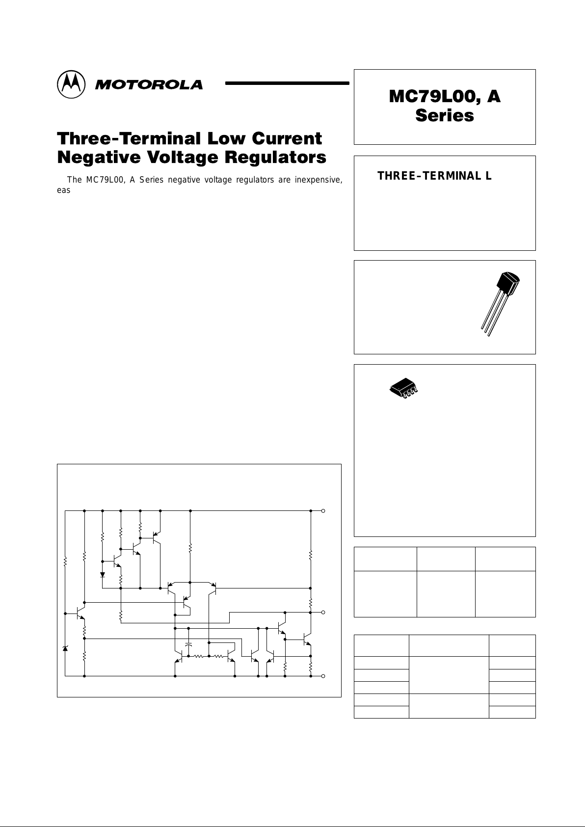
Representative Schematic Diagram
* Automotive temperature range selections are available with special test conditions
* and additional tests in 5, 12 and 15 V devices. Contact your local Motorola sales
* office for information.
R1
R2
Z1
R3
R
5
R18
Q1
R6
Q4
R7
R4
R8
Q5
Q10
Q8R9Q14
Q9
C
Q6
R10 R11
Q7Q2Q11
R14 R15
Q13
Q12
R16
R17
Gnd
Output
Input
Motorola, Inc. 1996 Rev 2

MC79L00, A Series
2
MOTOROLA ANALOG IC DEVICE DATA
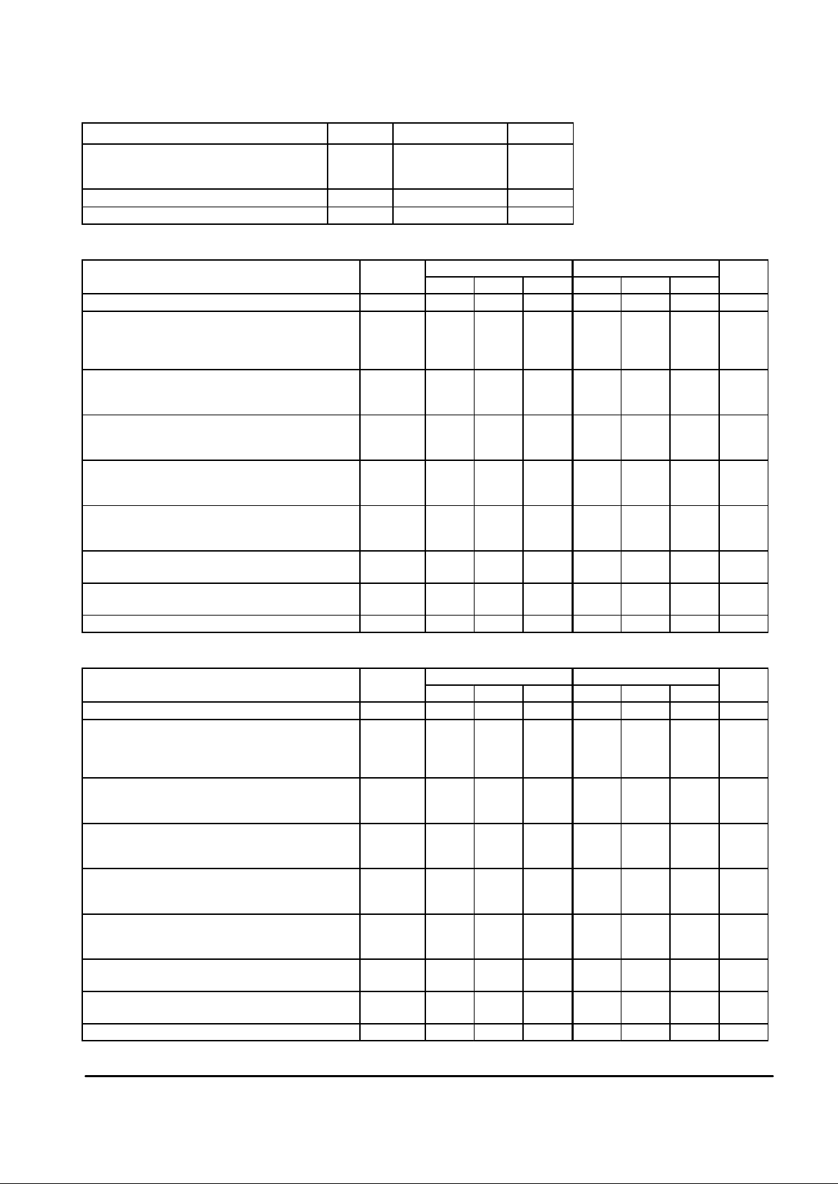
MAXIMUM RATINGS
(TA = +25°C, unless otherwise noted.)
Rating
Symbol Value Unit
Input Voltage (–5 V)
Input Voltage (–12, –15, –18 V)
Input Voltage (–24 V)
V
I
–30
–35
–40
Vdc
Storage Temperature Range T
stg
–65 to +150 °C
Junction Temperature T
J
+150 °C
ELECTRICAL CHARACTERISTICS (V
I
= –10 V , IO = 40 mA, CI = 0.33 µF, CO = 0.1 µF, –40°C < TJ +125°C (for MC79LXXAB),
0°C < TJ < +125°C (for MC79LXXAC)).
MC79L05C, AB MC79L05AC, AB
Characteristics Symbol Min Typ Max Min Typ Max Unit
Output Voltage (TJ = +25°C) V
O
–4.6 –5.0 –5.4 –4.8 –5.0 –5.2 Vdc
Input Regulation
(TJ = +25°C)
–7.0 Vdc ≥ VI ≥ –20 Vdc
–8.0 Vdc ≥ VI ≥ –20 Vdc
Reg
line
–
–
–
–
200
150
–
–
–
–
150
100
mV
Load Regulation
TJ = +25°C, 1.0 mA ≤ IO ≤ 100 mA
1.0 mA ≤ IO ≤ 40 mA
Reg
load
–
–
–
–
60
30
–
–
–
–
60
30
mV
Output Voltage
–7.0 Vdc ≥ VI ≥ –20 Vdc, 1.0 mA ≤ IO ≤ 40 mA
VI = –10 Vdc, 1.0 mA ≤ IO ≤ 70 mA
V
O
–4.5
–4.5
–
–
–5.5
–5.5
–4.75
–4.75
–
–
–5.25
–5.25
Vdc
Input Bias Current
(TJ = +25°C)
(TJ = +125°C)
I
IB
–
–
–
–
6.0
5.5
–
–
–
–
6.0
5.5
mA
Input Bias Current Change
–8.0 Vdc ≥ VI ≥ –20 Vdc
1.0 mA ≤ IO ≤ 40 mA
I
IB
–
–
–
–
1.5
0.2
–
–
–
–
1.5
0.1
mA
Output Noise Voltage
(TA = +25°C, 10 Hz ≤ f ≤ 100 kHz)
V
n
– 40 – – 40 – µV
Ripple Rejection
(–8.0 ≥ VI ≥ –18 Vdc, f = 120 Hz, TJ = +25°C)
RR 40 49 – 41 49 – dB
Dropout Voltage (IO = 40 mA, TJ = +25°C) |VI–VO| – 1.7 – – 1.7 – Vdc
ELECTRICAL CHARACTERISTICS (V
I
= –19 V , IO = 40 mA, CI = 0.33 µF, CO = 0.1 µF, –40°C < TJ +125°C (for MC79LXXAC),
0°C < TJ < +125°C (for MC79LXXAB)).
MC79L12C, AB MC79L12AC, AB
Characteristics Symbol Min Typ Max Min Typ Max Unit
Output Voltage (TJ = +25°C) V
O
–11.1 –12 –12.9 –1 1.5 –12 –12.5 Vdc
Input Regulation
(TJ = +25°C)
–14.5 Vdc ≥ VI ≥ –27 Vdc
–16 Vdc ≥ VI ≥ –27 Vdc
Reg
line
–
–
–
–
250
200
–
–
–
–
250
200
mV
Load Regulation
TJ = +25°C, 1.0 mA ≤ IO ≤ 100 mA
1.0 mA ≤ IO ≤ 40 mA
Reg
load
–
–
–
–
100
50
–
–
–
–
100
50
mV
Output Voltage
–14.5 Vdc ≥ VI ≥ –27 Vdc, 1.0 mA ≤ IO ≤ 40 mA
VI = –19 Vdc, 1.0 mA ≤ IO ≤ 70 mA
V
O
–10.8
–10.8
–
–
–13.2
–13.2
–11.4
–11.4
–
–
–12.6
–12.6
Vdc
Input Bias Current
(TJ = +25°C)
(TJ = +125°C)
I
IB
–
–
–
–
6.5
6.0
–
–
–
–
6.5
6.0
mA
Input Bias Current Change
–16 Vdc ≥ VI ≥ –27 Vdc
1.0 mA ≤ IO ≤ 40 mA
I
IB
–
–
–
–
1.5
0.2
–
–
–
–
1.5
0.2
mA
Output Noise Voltage
(TA = +25°C, 10 Hz ≤ f ≤ 100 kHz)
V
n
– 80 – – 80 – µV
Ripple Rejection
(–15 ≤ VI ≤ –25 Vdc, f = 120 Hz, TJ = +25°C)
RR 36 42 – 37 42 – dB
Dropout Voltage (IO = 40 mA, TJ = +25°C) |VI–VO| – 1.7 – – 1.7 – Vdc
 Loading...