

Motorola TPV8200B Datasheet
1
TPV8200BMOTOROLA RF DEVICE DATA
The RF Line
The TPV8200B is designed for output stages in band IV and V TV transmitter
amplifiers. It incorporates high value emitter ballast resistors, gold metallizations and offers a high degree of reliability and ruggedness.
Including input and output matching networks, the TPV8200B features high
impedances. It can operate over the 470 MHz to 860 MHz bandwidth using a
single fixed tuned circuit.
• To be used class AB for TV band IV and V.
• Specified 28 Volts, 860 MHz Characteristics
Output Power = 190 Watts (peak sync.)
Output Power = 150 Watts (CW)
Gain = 8 dB Min
• Circuit board photomaster available upon request by contacting
RF Tactical Marketing in Phoenix, AZ.
MAXIMUM RATINGS
Rating Symbol Value Unit
Collector–Emitter Voltage V
CEO
30 Vdc
Collector–Base Voltage V
CBO
65 Vdc
Emitter–Base Voltage V
EBO
4 Vdc
Collector–Current — Continuous I
C
20 Adc
Total Device Dissipation @ TC = 25°C
Derate above 25°C
P
D
250
1.43
Watts
W/°C
Quiescent Current (without RF drive) I
CQ
2 x 500 mAdc
Storage Temperature Range T
stg
–65 to +150 °C
THERMAL CHARACTERISTICS
Characteristic Symbol Max Unit
Thermal Resistance, Junction to Case (1) R
θJC
0.7 °C/W
ELECTRICAL CHARACTERISTICS (T
C
= 25°C unless otherwise noted)
Characteristic
Symbol Min Typ Max Unit
OFF CHARACTERISTICS
Collector–Emitter Breakdown Voltage
(IC = 20 mAdc, IB = 0)
V
(BR)CEO
30 35 — Vdc
Collector–Base Breakdown Voltage
(IC = 20 mAdc, IE = 0)
V
(BR)CBO
65 80 — Vdc
Emitter–Base Breakdown Voltage (IE = 20 mAdc, IC = 0) V
(BR)EBO
4 5 — Vdc
Collector–Emitter Leakage Current (VCE = 28 Vdc, RBE = 75 Ω) I
CER
— — 15 mAdc
NOTE: (continued)
1. Thermal resistance is determined under specific RF condition.
Teflon is a registered trademark of du Pont de Nemours & Co., Inc.
Preferred devices are Motorola recommended choices for future use and best overall value.
Order this document
by TPV8200B/D
SEMICONDUCTOR TECHNICAL DATA
190 W, 470–860 MHz
RF POWER TRANSISTOR
NPN SILICON
CASE 375A–01, STYLE 1
Motorola Preferred Device
Motorola, Inc. 1994
REV 6
TPV8200B
2
MOTOROLA RF DEVICE DATA
ELECTRICAL CHARACTERISTICS — continued (T
C
= 25°C unless otherwise noted)
Characteristic
Symbol Min Typ Max Unit
ON CHARACTERISTICS
DC Current Gain (ICE = 2 Adc, VCE = 10 Vdc) h
FE
30 75 120 —
DYNAMIC CHARACTERISTICS
Output Capacitance (each side) (2)
(VCB = 28 Vdc, IE = 0, f = 1 MHz)
C
ob
— 76 — pF
FUNCTIONAL TESTS IN CW
Common–Emitter Amplifier Power Gain
(VCE = 28 Vdc, P
out
= 150 W, ICQ = 2 x 75 mA, f = 860 MHz)
G
pe
8 9.5 — dB
Collector Efficiency
(VCE = 28 Vdc, P
out
= 150 W, ICQ = 2 x 75 mA, f = 860 MHz)
η 45 53 — %
Output Power @ 1 dB Compression (P
ref
= 40 W)
(VCE = 28 Vdc, ICQ = 2 x 75 mA, f = 860 MHz)
P
out
150 165 — W
Input overdrive: no degradation
(VCE = 28 Vdc, ICQ = 2 x 75 mA, f = 860 MHz)
P
in
30 — — W
Output Mismatch Stress:
(VCE = 28 Vdc, P
out
= 120 W, ICQ = 2 x 75 mA, f = 860 MHz,
Load VSWR = 3:1, all phase angles at frequency of test)
ψ
No Degradation in Output Power
Before or After Test
FUNCTIONAL TESTS IN VIDEO (Standard Black Level)
Peak Output Power @ 1 dB Compression
(VCE = 28 Vdc, ICQ = 2 x 75 mA, f = 860 MHz)
P
out
190 210 — W
NOTE:
2. Value of “Cob” is that of die only. It is not measurable in TPV8200B because of internal matching network.
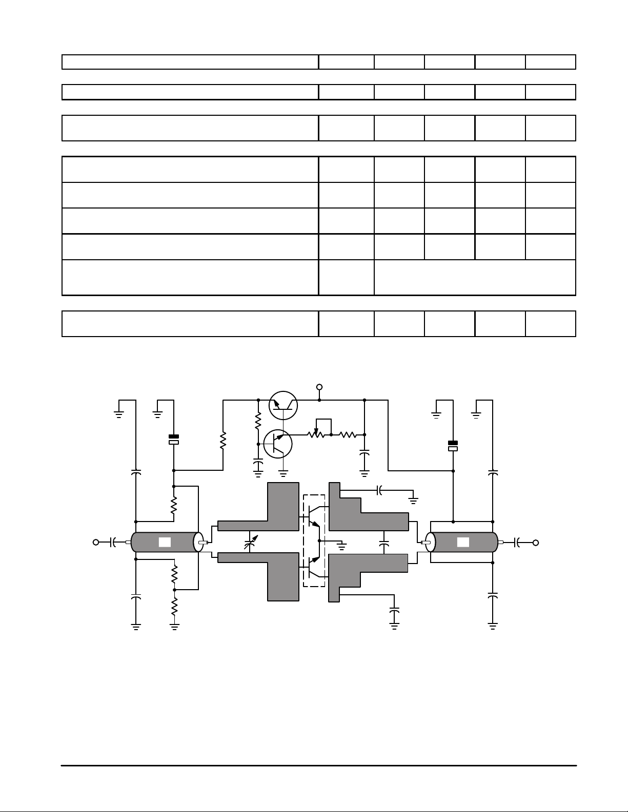
Figure 1. 860 MHz Test Circuit
INPUT OUTPUT
C1
C6
C6
C8
R2
R2
R1
R3
R4
C10
T1
T2
P1
R5
C11
C3
C4
C3
C9
C7
C5
C7
C2
V
CC
L1 L2
C1 — Chip Capacitor 47 pF ATC 100A
C2 — Chip Capacitor 12 pF ATC 100B
C2 — + Trimmer Capacitor 0.5–4 pF
C3 — Chip Capacitor 8.2 pF ATC 100B
C4 — Chip Capacitor 12 pF ATC 100B
C5 — Chip Capacitor 100 pF ATC 100A
C6 — Chip Capacitor 2 x 1000 pF Vitramon
C7 — Chip Capacitor 2 x 0.1 µF Vitramon
C8 — Capacitor 220 µF/16 V
C9 — Capacitor 100 µF/40 V
C10 — Chip Capacitor 100 pF Vitramon
C11 — Chip Capacitor 15 nF Vitramon
L1 — Coaxial 25 Ω/length = 41 mm
L2 — Coaxial 25 Ω/length = 41 mm
R1 — Chip Resistor 47 Ω
R2 — 2 x 1 Ω (0.5 Ω)
R3 — Resistor 0.8 Ω
R4 — Resistor 47 Ω
R5 — Resistor 1.2 kΩ
P1 — Trimmer Resistor 5 kΩ
T1 — Transistor BD 135
T2 — Transistor BD 135
PC Board: 1/50″ Glass Teflon ∈r = 2.55
D.U.T.
3
TPV8200BMOTOROLA RF DEVICE DATA
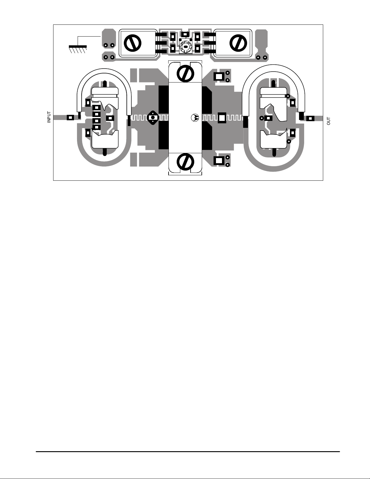
Figure 2. Components View
CAUTION
The TPV8200B is a high power transistor and thermal adaptation is very important for good RF performance
(see mechanical drawing for mounting recommendations).
Maximum Ratings are given to avoid destruction of the transistor; another limitation is MMMTBF and the
user must first determine the minimum wanted life–time in order to choose the right way of use for the device
(see MMMTBF curves), especially in case of CW application.
INPUT
OUTPUT
 Loading...