

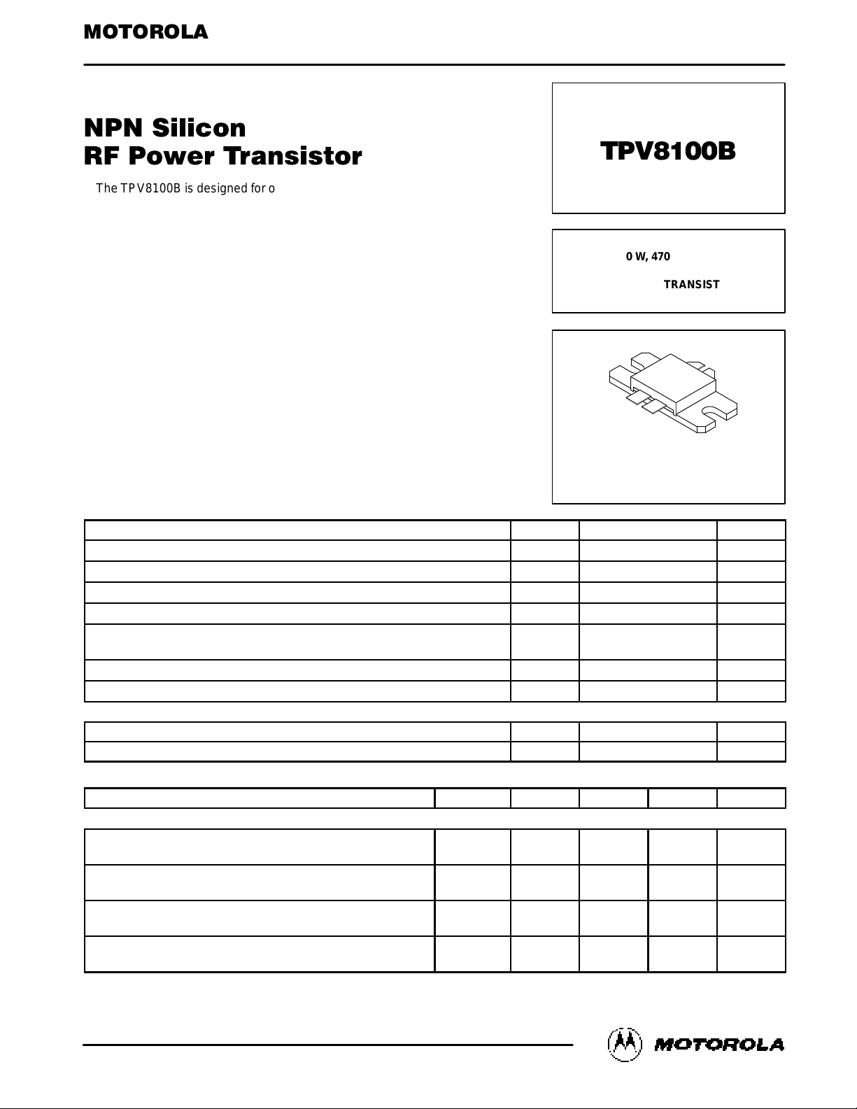
1
TPV8100BMOTOROLA RF DEVICE DATA
The RF Line
The TPV8100B is designed for output stages in band IV and V TV transmitter
amplifiers. It incorporates high value emitter ballast resistors, gold metallizations and offers a high degree of reliability and ruggedness.
Including d ouble i nput and output matching networks, t he TPV8100B
features high impedances. It can easily operate in a full 470 MHz to 860 MHz
bandwidth in a single and simple circuit.
• To be used class AB for TV band IV and V.
• Specified 28 Volts, 860 MHz Characteristics
Output Power = 125 Watts (peak sync.)
Output Power = 100 Watts (CW)
Minimum Gain = 8.5 dB
• Specified 32 Volts, 860 MHz Characteristics
Output Power = 150 Watts (peak sync.)
• Circuit board photomaster available upon request by contacting
RF Tactical Marketing in Phoenix, AZ.
MAXIMUM RATINGS
Rating Symbol Value Unit
Collector–Emitter Voltage V
CER
40 Vdc
Collector–Base Voltage V
CBO
65 Vdc
Emitter–Base Voltage V
EBO
4 Vdc
Collector–Current — Continuous I
C
12 Adc
Total Device Dissipation @ 25°C Case
Derate above 25°C
P
D
215
1.25
Watts
W/°C
Operating Junction Temperature T
J
200 °C
Storage Temperature Range T
stg
–65 to +150 °C
THERMAL CHARACTERISTICS
Characteristic Symbol Max Unit
Thermal Resistance, Junction to Case (1) R
θJC
0.8 °C/W
ELECTRICAL CHARACTERISTICS (T
C
= 25°C unless otherwise noted)
Characteristic
Symbol Min Typ Max Unit
OFF CHARACTERISTICS
Collector–Emitter Breakdown Voltage
(IC = 10 mA, Rbe = 75 Ω)
V
(BR)CER
30 — — Vdc
Collector–Emitter Breakdown Voltage
(IC = 10 mAdc)
V
(BR)EBO
4 — — Vdc
Collector–Base Breakdown Voltage
(IE = 20 mAdc)
V
(BR)CBO
65 — — Vdc
Collector–Emitter Leakage
(VCE = 28 V, Rbe = 75 Ω)
I
CER
— — 10 mA
NOTE: (continued)
1. Thermal resistance is determined under specified RF operating condition.
Order this document
by TPV8100B/D
SEMICONDUCTOR TECHNICAL DATA
150 W, 470–860 MHz
NPN SILICON
RF POWER TRANSISTOR
CASE 398–03, STYLE 1
Motorola, Inc. 1994
REV 6
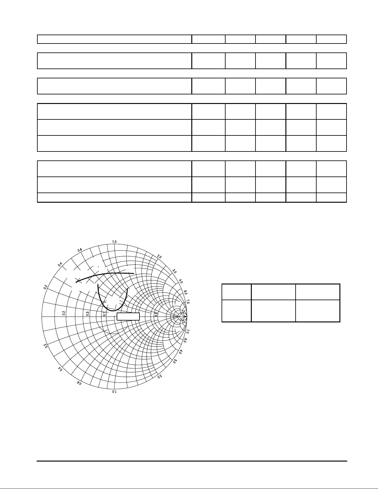
Figure 1. Series Equivalent Input/Output Impedances
Input and Output impedances with circuit tuned for maximum linearity @ VCC = 28 V / ICQ = 2 x 50 mA / P
out
= 100 W
0.0
8
470
860665
f = 470 MHz
f = 860 MHz
ZOL*
665
Zo = 10
Ω
Z
in
TPV8100B
2
MOTOROLA RF DEVICE DATA
ELECTRICAL CHARACTERISTICS — continued (T
C
= 25°C unless otherwise noted)
Characteristic
Symbol Min Typ Max Unit
ON CHARACTERISTICS
DC Current Gain
(IC = 2 Adc, VCE = 10 Vdc)
h
FE
30 — 120 —
DYNAMIC CHARACTERISTICS
Output Capacitance (each side) (2)
(VCB = 28 V, IE = 0, f = 1 MHz)
C
ob
— 44 — pF
FUNCTIONAL TESTS IN CW (SOUND)
Common–Emitter Amplifier Power Gain
(VCC = 28 V, P
out
= 100 W, ICQ = 2 x 50 mA, f = 860 MHz)
G
p
8.5 9.5 — dB
Collector Efficiency
(VCC = 28 V, P
out
= 100 W, IQ = 2 x 50 mA, f = 860 MHz)
η 55 58 — %
Output Power @ 1 dB Compression (P
ref
= 25 W)
(VCC = 28 V, ICQ = 2 x 50 mA, f = 860 MHz)
P
out
100 110 — W
FUNCTIONAL TESTS IN VIDEO (STANDARD BLACK LEVEL)
Peak Output Power (synch.)
(VCC = 28 V, ICQ = 2 x 50 mA, f = 860 MHz)
P
out
125 135 — W
Peak Output Power (synch.)
(VCC = 32 V, ICQ = 2 x 25 mA, f = 860 MHz)
P
out
150 160 — W
Recommended Quiescent Current I
CQ
— — 2 x 0.3 A
NOTE:
2. Value of “Cob” is that of die only. It is not measurable in TPV8100B because of internal matching network.
f
(MHz)
Z
in
(Ohms)
ZOL*
(Ohms)
470 1.95 + j3.67 10.0 + j9.50
665 3.65 + j6.82 9.23 + j1.30
860 6.66 + j13.8 4.45 + j5.22
ZOL* = Conjugate of optimum load impedance into which
ZOL* = the device operates at a given output power,
ZOL* = voltage, current and frequency.
NOTE: Zin & ZOL* are given from base–to–base and
NOTE: collector–to–collector respectively.
 Loading...