

Motorola TPV596A Datasheet
1
TPV596AMOTOROLA RF DEVICE DATA
The RF Line
. . . designed for very high output 1.5 V MATV amplifiers up to 860 MHz and
500 mW Band V TV transposer stages. Gold metallization and diffused emitter
ballast resistors are used to enhanced reliability, ruggedness and linearity.
• Band IV and V (470–860 MHz)
• 0.5 W — P
ref
@ –58 dB IMD
• High Gain — 12 dB Typ, Class A, f = 860 MHz
• Gold Metallization for Reliability
MAXIMUM RATINGS
Rating Symbol Value Unit
Collector–Emitter Voltage V
CEO
24 Vdc
Collector–Base Voltage V
CBO
45 Vdc
Emitter–Base Voltage V
EBO
3.5 Vdc
Collector Current — Continuous I
C
0.7 Adc
Total Device Dissipation @ TC = 25°C
Derate above 25°C
P
D
8.75
0.05
Watts
W/°C
Operating Junction Temperature T
J
200 °C
Storage Temperature Range T
stg
–65 to +200 °C
THERMAL CHARACTERISTICS
Characteristic Symbol Max Unit
Thermal Resistance, Junction to Case (TC = 70°C) R
θJC
20 °C/W
ELECTRICAL CHARACTERISTICS
Characteristic Symbol Min Typ Max Unit
OFF CHARACTERISTICS
Collector–Emitter Breakdown Voltage
(IC = 20 mA, IB = 0)
V
(BR)CEO
24 — — Vdc
Collector–Base Breakdown Voltage
(IC = 1.0 mA, IE = 0)
V
(BR)CBO
45 — — Vdc
Emitter–Base Breakdown Voltage
(IE = 4.0 mA, IC = 0)
V
(BR)EBO
3.5 — — Vdc
Emitter–Base Leakage Current
(VEB = 2.0 V)
I
EBO
— — 0.25 mA
Collector Cutoff Current
(VCB = 28 V, IE = 0)
I
CBO
— — 1.0 mAdc
Collector–Emitter Breakdown Voltage
(IC = 20 mA, RBE = 10 Ω)
V
(BR)CER
50 — — Vdc
ON CHARACTERISTICS
DC Current Gain
(IC = 100 mA, VCE = 5.0 V)
h
FE
15 — 120 —
DYNAMIC CHARACTERISTICS
Output Capacitance
(VCB = 28 V, IE = 0, f = 1.0 MHz)
C
ob
— — 5.0 pF
(continued)
Order this document
by TPV596A/D
SEMICONDUCTOR TECHNICAL DATA
0.5 W, 470–860 MHz
UHF LINEAR
POWER TRANSISTOR
CASE 244–04, STYLE 1
(.280 SOE)
Motorola, Inc. 1994
TPV596A
2
MOTOROLA RF DEVICE DATA
ELECTRICAL CHARACTERISTICS — continued
Characteristic UnitMaxTypMinSymbol
FUNCTIONAL TESTS
Common–Emitter Amplifier Power Gain
(VCE = 20 V, P
out
= 0.5 W, f = 860 MHz, IE = 0.22 A)
G
PE
11.5 12 — dB
Load Mismatch
(VCE = 20 V, P
out
= 1.0 W, IE = 0.22 A, f = 860 MHz,
Load VSWR = ∞:1, All Phase Angles)
ψ
No Degradation in Output Power
Intermodulation Distortion, 3 Tone
(f = 860 MHz, VCE = 20 V, IE = 0.22 A, P
ref
= 1.0 W,
Vision Carrier = –8.0 dB, Sound Carrier = –7.0 dB,
Sideband Signal = –16 dB, Specification TV05001)
IMD
1
— — –50 dB
Intermodulation Distortion (IDEM)
(f = 860 MHz, VCE = 20 V, IE = 0.22 A, P
ref
= 0.5 W,
Vision Carrier = –8.0 dB, Sound Carrier = –10 dB,
Sideband Signal = –16 dB)
IMD
2
—
–ā60 –ā58
dB
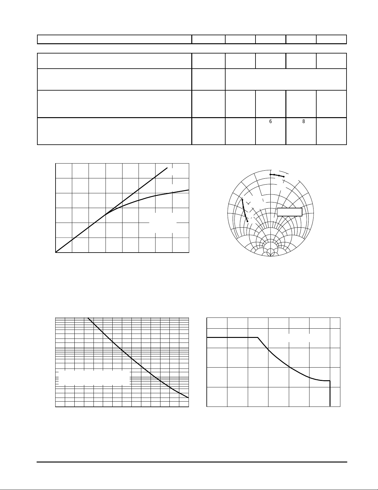
Figure 1. Power Output versus Power Input Figure 2. Large Signal Impedances
VCE = 20 V — IC = 220 mA
Figure 3. MTTF Factor versus Junction
Temperature
Figure 4. DC Safe Operating Area
ZOL* = Conjugate of the optimum load impedance into which the
device output operates at a given output power, voltage and
frequency.
P , OUTPUT POWER (WATTS)
out
I
C
, COLLECTOR CURRENT (A)
MTTF FACTOR (10
2
)
6
HRS x AMP
100
TJ, JUNCTION TEMPERATURE (°C)
120 140 160 180 200
1
80
0.1
0.01
0.001
Pin, INPUT POWER (mW)
20340 60 80 100 120 140
2.5
2
1.5
1
0.5
0
6
4
2
4
VCE, COLLECTOR–EMITTER VOLTAGE (VOLTS)
8
8 12 16 20 24
NOTE: DIVIDE MTTF BY I
C
2
TO
NOTE: OBTAIN METAL LIFE
f = 860 MHz
VCE = 20 V
IC = 220 mA
IDEAL
REAL
T
HEATSINK
= 70°C
0
0.2
0.4
0.6
0.8
1
1.5
2
3
4
5
10
0
10
3
4
5
2
1.5
1
0.8
0.6
0.4
0.2
0.6
0.4
f = 1 GHz
Z
in
0.8
f = 1 GHz
ZOL*
0.4
0.6
0.4
0.6
1
1.5
2
3
4
5
10
TYPICAL CHARACTERISTICS
0.8
0.8
0.1
0.2
Zo = 50
Ω
 Loading...