

Page 1

Technical Information
Motorola H24 Developer’s Guide
Module Hardware Description
NOVEMBER 15, 2009
6802986C38-D
Page 2

Notice
While reasonable efforts have been made to assure the accuracy of this document, Motorola, Inc. assumes no liability resulting
from any inaccuracies or omissions in this document, or from use of the information obtained herein. The information in this
document has been carefully checked and is believed to be entirely reliable. However, no responsibility is assumed for
inaccuracies or omissions. Motorola, Inc. reserves the right to make changes to any products described herein and reserves the
right to revise this document and to make changes from time to time in content hereof with no obligation to notify any person of
revisions or changes. Motorola, Inc. does not assume any liability arising out of the application or use of any product, software, or
circuit described herein; neither does it convey license under its patent rights or the rights of others.
It is possible that this publication may contain references to, or information about Motorola products (machines and programs),
programming, or services that are not announced in your country. Such references or information must not be construed to mean
that Motorola intends to announce such Motorola products, programming, or services in your country.
Copyrights
This instruction manual, and the Motorola products described in this instruction manual may be, include or describe copyrighted
Motorola material, such as computer programs stored in semiconductor memories or other media. Laws in the United States and
other countries preserve for Motorola and its licensors certain exclusive rights for copyrighted material, including the exclusive
right to copy, reproduce in any form, distribute and make derivative works of the copyrighted material. Accordingly, any
copyrighted material of Motorola and its licensors contained herein or in the Motorola products described in this instruction
manual may not be copied, reproduced, distributed, merged or modified in any manner without the express written permission of
Motorola. Furthermore, the purchase of Motorola products shall not be deemed to grant either directly or by implication, estoppel,
or otherwise, any license under the copyrights, patents or patent applications of Motorola, as arises by operation of law in the sale
of a product.
SPECIFICATIONS SUBJECT TO CHANGE WITHOUT NOTICE
Computer Software Copyrights
The Motorola and 3rd Party supplied Software (SW) products described in this instruction manual may include copyrighted
Motorola and other 3rd Party supplied computer programs stored in semiconductor memories or other media. Laws in the United
States and other countries preserve for Motorola and other 3rd Party supplied SW certain exclusive rights for copyrighted
computer programs, including the exclusive right to copy or reproduce in any form the copyrighted computer program.
Accordingly, any copyrighted Motorola or other 3rd Party supplied SW computer programs contained in the Motorola products
described in this instruction manual may not be copied (reverse engineered) or reproduced in any manner without the express
written permission of Motorola or the 3rd Party SW supplier. Furthermore, the purchase of Motorola products shall not be deemed
to grant either directly or by implication, estoppel, or otherwise, any license under the copyrights, patents or patent applications of
Motorola or other 3rd Party supplied SW, except for the normal non-exclusive, royalty free license to use that arises by operation
of law in the sale of a product.
VENDOR COPYRIGHT
Apache Software Foundation Copyright 2004-2005 All Rights Reserved
Page 3

Usage and Disclosure Restrictions
License Agreements
The software described in this document is the property of Motorola, Inc. and its licensors. It is furnished by express license
agreement only and may be used only in accordance with the terms of such an agreement.
Copyrighted Materials
Software and documentation are copyrighted materials. Making unauthorized copies is prohibited by law. No part of the software
or documentation may be reproduced, transmitted, transcribed, stored in a retrieval system, or translated into any language or
computer language, in any form or by any means, without prior written permission of Motorola, Inc.
High Risk Materials
Components, units, or third-party products used in the product described herein are NOT fault-tolerant and are NOT designed,
manufactured, or intended for use as on-line control equipment in the following hazardous environments requiring fail-safe
controls: the operation of Nuclear Facilities, Aircraft Navigation or Aircraft Communication Systems, Air Traffic Control, Life
Support, or Weapons Systems (High Risk Activities"). Motorola and its supplier(s) specifically disclaim any expressed or implied
warranty of fitness for such High Risk Activities.
Trademarks
MOTOROLA and the Stylized M Logo are registered in the US Patent & Trademark Office. All other product or service names are
the property of their respective owners.
© Copyright 2009 Motorola, Inc.
REV052604
Page 4

Page 5

Table of Contents
Manual Scope . . . . . . . . . . . . . . . . . . . . . . . . . . . . . . . . . . . . . . . . . . . . . . . . . . . . . . . . . . . . . . . . . . . vii
Target Audience . . . . . . . . . . . . . . . . . . . . . . . . . . . . . . . . . . . . . . . . . . . . . . . . . . . . . . . . . . . . . . . . . vii
Manual Organization . . . . . . . . . . . . . . . . . . . . . . . . . . . . . . . . . . . . . . . . . . . . . . . . . . . . . . . . . . . . . . vii
Applicable Documents . . . . . . . . . . . . . . . . . . . . . . . . . . . . . . . . . . . . . . . . . . . . . . . . . . . . . . . . . . . . vii
Regulatory Requirements . . . . . . . . . . . . . . . . . . . . . . . . . . . . . . . . . . . . . . . . . . . . . . . . . . . . . . . . . viii
Regulatory Statement (Safety). . . . . . . . . . . . . . . . . . . . . . . . . . . . . . . . . . . . . . . . . . . . . . . . . . . . . . viii
FCC Notice to Users . . . . . . . . . . . . . . . . . . . . . . . . . . . . . . . . . . . . . . . . . . . . . . . . . . . . . . . . . . . . . viii
Precautions. . . . . . . . . . . . . . . . . . . . . . . . . . . . . . . . . . . . . . . . . . . . . . . . . . . . . . . . . . . . . . . . . . . . . . .ix
Antenna and Transmission Safety Precautions . . . . . . . . . . . . . . . . . . . . . . . . . . . . . . . . . . . . . . . . . . .ix
Standards . . . . . . . . . . . . . . . . . . . . . . . . . . . . . . . . . . . . . . . . . . . . . . . . . . . . . . . . . . . . . . . . . . . . . . . . x
Contact Us . . . . . . . . . . . . . . . . . . . . . . . . . . . . . . . . . . . . . . . . . . . . . . . . . . . . . . . . . . . . . . . . . . . . . . .xi
Text Conventions. . . . . . . . . . . . . . . . . . . . . . . . . . . . . . . . . . . . . . . . . . . . . . . . . . . . . . . . . . . . . . . . . .xi
Field Service . . . . . . . . . . . . . . . . . . . . . . . . . . . . . . . . . . . . . . . . . . . . . . . . . . . . . . . . . . . . . . . . . . . xiii
General Safety . . . . . . . . . . . . . . . . . . . . . . . . . . . . . . . . . . . . . . . . . . . . . . . . . . . . . . . . . . . . . . . . . . xiii
Caring for the Environment. . . . . . . . . . . . . . . . . . . . . . . . . . . . . . . . . . . . . . . . . . . . . . . . . . . . . . . . .xiv
Limitation of Liability . . . . . . . . . . . . . . . . . . . . . . . . . . . . . . . . . . . . . . . . . . . . . . . . . . . . . . . . . . . . . xv
Warranty Notification . . . . . . . . . . . . . . . . . . . . . . . . . . . . . . . . . . . . . . . . . . . . . . . . . . . . . . . . . . . . . xv
How to Get Warranty Service? . . . . . . . . . . . . . . . . . . . . . . . . . . . . . . . . . . . . . . . . . . . . . . . . . . . . . .xvi
Claiming . . . . . . . . . . . . . . . . . . . . . . . . . . . . . . . . . . . . . . . . . . . . . . . . . . . . . . . . . . . . . . . . . . . . . . .xvi
Conditions . . . . . . . . . . . . . . . . . . . . . . . . . . . . . . . . . . . . . . . . . . . . . . . . . . . . . . . . . . . . . . . . . . . . . xvii
What is Not Covered by the Warranty . . . . . . . . . . . . . . . . . . . . . . . . . . . . . . . . . . . . . . . . . . . . . . . xvii
Installed Data. . . . . . . . . . . . . . . . . . . . . . . . . . . . . . . . . . . . . . . . . . . . . . . . . . . . . . . . . . . . . . . . . . xviii
Out of Warranty Repairs . . . . . . . . . . . . . . . . . . . . . . . . . . . . . . . . . . . . . . . . . . . . . . . . . . . . . . . . . xviii
Revision History . . . . . . . . . . . . . . . . . . . . . . . . . . . . . . . . . . . . . . . . . . . . . . . . . . . . . . . . . . . . . . . . .xix
Chapter 1: Introduction . . . . . . . . . . . . . . . . . . . . . . . . . . . . . . . . . . . . . . . . . . . . . . . . . . . . . . . . . . . . . 1
Product Specifications . . . . . . . . . . . . . . . . . . . . . . . . . . . . . . . . . . . . . . . . . . . . . . . . . . . . . . . . . . . . . . 2
Regulatory Approvals . . . . . . . . . . . . . . . . . . . . . . . . . . . . . . . . . . . . . . . . . . . . . . . . . . . . . . . . . . . . . . 6
European Union Directives Conformance Statement . . . . . . . . . . . . . . . . . . . . . . . . . . . . . . . . . . . 6
CFR 47 Part 15.19 specifies label requirements . . . . . . . . . . . . . . . . . . . . . . . . . . . . . . . . . . . . . . . 6
CFR 47 Part 15.21 Information to user . . . . . . . . . . . . . . . . . . . . . . . . . . . . . . . . . . . . . . . . . . . . . . 7
CFR 47 Part 15.105 Information to the user . . . . . . . . . . . . . . . . . . . . . . . . . . . . . . . . . . . . . . . . . . 7
Chapter 2: Hardware Interface Description . . . . . . . . . . . . . . . . . . . . . . . . . . . . . . . . . . . . . . . . . . . . . 9
Architecture Overview . . . . . . . . . . . . . . . . . . . . . . . . . . . . . . . . . . . . . . . . . . . . . . . . . . . . . . . . . . . . . 9
Digital Block . . . . . . . . . . . . . . . . . . . . . . . . . . . . . . . . . . . . . . . . . . . . . . . . . . . . . . . . . . . . . . . . . 10
Analog Block . . . . . . . . . . . . . . . . . . . . . . . . . . . . . . . . . . . . . . . . . . . . . . . . . . . . . . . . . . . . . . . . . 10
RF Transceiver Block . . . . . . . . . . . . . . . . . . . . . . . . . . . . . . . . . . . . . . . . . . . . . . . . . . . . . . . . . . 11
WCDMA Transceiver . . . . . . . . . . . . . . . . . . . . . . . . . . . . . . . . . . . . . . . . . . . . . . . . . . . . . . . . 12
Operating Modes . . . . . . . . . . . . . . . . . . . . . . . . . . . . . . . . . . . . . . . . . . . . . . . . . . . . . . . . . . . . . . . . . 13
Power Supply. . . . . . . . . . . . . . . . . . . . . . . . . . . . . . . . . . . . . . . . . . . . . . . . . . . . . . . . . . . . . . . . . . . . 14
Power Supply Design . . . . . . . . . . . . . . . . . . . . . . . . . . . . . . . . . . . . . . . . . . . . . . . . . . . . . . . . . . . 14
Current Consumption . . . . . . . . . . . . . . . . . . . . . . . . . . . . . . . . . . . . . . . . . . . . . . . . . . . . . . . . . . . 16
Power On/Off Operation . . . . . . . . . . . . . . . . . . . . . . . . . . . . . . . . . . . . . . . . . . . . . . . . . . . . . . . . . . . 18
November 15, 2009 H24 - Module Hardware Description i
Page 6

Ta ble of Contents
Low Power Mode. . . . . . . . . . . . . . . . . . . . . . . . . . . . . . . . . . . . . . . . . . . . . . . . . . . . . . . . . . . . . . . . . 20
Real Time Clock . . . . . . . . . . . . . . . . . . . . . . . . . . . . . . . . . . . . . . . . . . . . . . . . . . . . . . . . . . . . . . . . . 24
Serial Interfaces . . . . . . . . . . . . . . . . . . . . . . . . . . . . . . . . . . . . . . . . . . . . . . . . . . . . . . . . . . . . . . . . . . 25
SIM Interface . . . . . . . . . . . . . . . . . . . . . . . . . . . . . . . . . . . . . . . . . . . . . . . . . . . . . . . . . . . . . . . . . . . . 27
Audio Interface . . . . . . . . . . . . . . . . . . . . . . . . . . . . . . . . . . . . . . . . . . . . . . . . . . . . . . . . . . . . . . . . . . 29
Controls and Indicators Interface. . . . . . . . . . . . . . . . . . . . . . . . . . . . . . . . . . . . . . . . . . . . . . . . . . . . . 35
Antenna Interface. . . . . . . . . . . . . . . . . . . . . . . . . . . . . . . . . . . . . . . . . . . . . . . . . . . . . . . . . . . . . . . . . 39
Turning the H24 On . . . . . . . . . . . . . . . . . . . . . . . . . . . . . . . . . . . . . . . . . . . . . . . . . . . . . . . . . . . . 18
Power Supply Turn-on . . . . . . . . . . . . . . . . . . . . . . . . . . . . . . . . . . . . . . . . . . . . . . . . . . . . . . . . 18
Turning the H24 On Using ON_N . . . . . . . . . . . . . . . . . . . . . . . . . . . . . . . . . . . . . . . . . . . . . . . 18
Turning the H24 On Using IGN . . . . . . . . . . . . . . . . . . . . . . . . . . . . . . . . . . . . . . . . . . . . . . . . . 19
Turning the H24 Off . . . . . . . . . . . . . . . . . . . . . . . . . . . . . . . . . . . . . . . . . . . . . . . . . . . . . . . . . . . . 19
Turning the H24 Off Using ON_N. . . . . . . . . . . . . . . . . . . . . . . . . . . . . . . . . . . . . . . . . . . . . . . 19
Turning the H24 Off Using IGN . . . . . . . . . . . . . . . . . . . . . . . . . . . . . . . . . . . . . . . . . . . . . . . . 19
Power Loss shut down . . . . . . . . . . . . . . . . . . . . . . . . . . . . . . . . . . . . . . . . . . . . . . . . . . . . . . . . 19
Turning the H24 Off Using AT+MPWRDN . . . . . . . . . . . . . . . . . . . . . . . . . . . . . . . . . . . . . . . 19
Activating Low Power Mode . . . . . . . . . . . . . . . . . . . . . . . . . . . . . . . . . . . . . . . . . . . . . . . . . . . . . 20
Serial Interface During Low Power Mode . . . . . . . . . . . . . . . . . . . . . . . . . . . . . . . . . . . . . . . . . . . 21
Terminating Low Power Mode . . . . . . . . . . . . . . . . . . . . . . . . . . . . . . . . . . . . . . . . . . . . . . . . . . .22
Temporary Termination of Low Power Mode . . . . . . . . . . . . . . . . . . . . . . . . . . . . . . . . . . . . . . 22
UART and USB Exiting of Low Power Mode. . . . . . . . . . . . . . . . . . . . . . . . . . . . . . . . . . . . . . 23
Primary UART (UART1) . . . . . . . . . . . . . . . . . . . . . . . . . . . . . . . . . . . . . . . . . . . . . . . . . . . . . . . . 25
USB Interface . . . . . . . . . . . . . . . . . . . . . . . . . . . . . . . . . . . . . . . . . . . . . . . . . . . . . . . . . . . . . . . . . 25
External SIM Connection . . . . . . . . . . . . . . . . . . . . . . . . . . . . . . . . . . . . . . . . . . . . . . . . . . . . . . . . 27
SIM Design Guidelines . . . . . . . . . . . . . . . . . . . . . . . . . . . . . . . . . . . . . . . . . . . . . . . . . . . . . . . . . 27
Embedded SIM . . . . . . . . . . . . . . . . . . . . . . . . . . . . . . . . . . . . . . . . . . . . . . . . . . . . . . . . . . . . . . . . 28
Handset Interface . . . . . . . . . . . . . . . . . . . . . . . . . . . . . . . . . . . . . . . . . . . . . . . . . . . . . . . . . . . . . . 29
Headset Interface . . . . . . . . . . . . . . . . . . . . . . . . . . . . . . . . . . . . . . . . . . . . . . . . . . . . . . . . . . . . . . 30
Interface to an External Speaker Amplifier . . . . . . . . . . . . . . . . . . . . . . . . . . . . . . . . . . . . . . . . . . 31
Audio Design . . . . . . . . . . . . . . . . . . . . . . . . . . . . . . . . . . . . . . . . . . . . . . . . . . . . . . . . . . . . . . . . . 32
Analog Ground . . . . . . . . . . . . . . . . . . . . . . . . . . . . . . . . . . . . . . . . . . . . . . . . . . . . . . . . . . . . . . 33
Digital Audio Interface . . . . . . . . . . . . . . . . . . . . . . . . . . . . . . . . . . . . . . . . . . . . . . . . . . . . . . . . . . 33
Voiceband Audio . . . . . . . . . . . . . . . . . . . . . . . . . . . . . . . . . . . . . . . . . . . . . . . . . . . . . . . . . . . . 33
Reset . . . . . . . . . . . . . . . . . . . . . . . . . . . . . . . . . . . . . . . . . . . . . . . . . . . . . . . . . . . . . . . . . . . . . . . . 35
VREF Reference Regulator . . . . . . . . . . . . . . . . . . . . . . . . . . . . . . . . . . . . . . . . . . . . . . . . . . . . . . 35
OFF Mode. . . . . . . . . . . . . . . . . . . . . . . . . . . . . . . . . . . . . . . . . . . . . . . . . . . . . . . . . . . . . . . . . . 36
Sleep Mode . . . . . . . . . . . . . . . . . . . . . . . . . . . . . . . . . . . . . . . . . . . . . . . . . . . . . . . . . . . . . . . . . 36
Active Mode . . . . . . . . . . . . . . . . . . . . . . . . . . . . . . . . . . . . . . . . . . . . . . . . . . . . . . . . . . . . . . . . 36
Wakeup Out . . . . . . . . . . . . . . . . . . . . . . . . . . . . . . . . . . . . . . . . . . . . . . . . . . . . . . . . . . . . . . . . . . 36
Network Connection Detection . . . . . . . . . . . . . . . . . . . . . . . . . . . . . . . . . . . . . . . . . . . . . . . . . . . 37
Transmission Indicator . . . . . . . . . . . . . . . . . . . . . . . . . . . . . . . . . . . . . . . . . . . . . . . . . . . . . . . . . . 38
General Purpose I/O . . . . . . . . . . . . . . . . . . . . . . . . . . . . . . . . . . . . . . . . . . . . . . . . . . . . . . . . . . . . 38
Chapter 3: Electrical and Environmental Specifications. . . . . . . . . . . . . . . . . . . . . . . . . . . . . . . . . .41
Absolute Maximum Ratings . . . . . . . . . . . . . . . . . . . . . . . . . . . . . . . . . . . . . . . . . . . . . . . . . . . . . . . . 41
Environmental Specifications . . . . . . . . . . . . . . . . . . . . . . . . . . . . . . . . . . . . . . . . . . . . . . . . . . . . . . . 42
Application Interface Specifications . . . . . . . . . . . . . . . . . . . . . . . . . . . . . . . . . . . . . . . . . . . . . . . . . . 42
Chapter 4: Mechanical Specifications. . . . . . . . . . . . . . . . . . . . . . . . . . . . . . . . . . . . . . . . . . . . . . . . .49
Board Dimensions . . . . . . . . . . . . . . . . . . . . . . . . . . . . . . . . . . . . . . . . . . . . . . . . . . . . . . . . . . . . . . . . 49
Interface Connector Specifications . . . . . . . . . . . . . . . . . . . . . . . . . . . . . . . . . . . . . . . . . . . . . . . . . . . 50
Mating Connector . . . . . . . . . . . . . . . . . . . . . . . . . . . . . . . . . . . . . . . . . . . . . . . . . . . . . . . . . . . . . . 51
MMCX Connector Specifications . . . . . . . . . . . . . . . . . . . . . . . . . . . . . . . . . . . . . . . . . . . . . . . . . . . . 52
Mating Connector . . . . . . . . . . . . . . . . . . . . . . . . . . . . . . . . . . . . . . . . . . . . . . . . . . . . . . . . . . . . . . 52
ii H24 - Module Hardware Description November 15, 2009
Page 7

Ta ble of Contents
U.FL Connector Specifications . . . . . . . . . . . . . . . . . . . . . . . . . . . . . . . . . . . . . . . . . . . . . . . . . . . . . . 54
Mating Connector . . . . . . . . . . . . . . . . . . . . . . . . . . . . . . . . . . . . . . . . . . . . . . . . . . . . . . . . . . . . . 55
H24 Mounting . . . . . . . . . . . . . . . . . . . . . . . . . . . . . . . . . . . . . . . . . . . . . . . . . . . . . . . . . . . . . . . . . . . 56
Chapter 5: Service and Testing. . . . . . . . . . . . . . . . . . . . . . . . . . . . . . . . . . . . . . . . . . . . . . . . . . . . . . 57
Service . . . . . . . . . . . . . . . . . . . . . . . . . . . . . . . . . . . . . . . . . . . . . . . . . . . . . . . . . . . . . . . . . . . . . . . . . 57
Who to Contact? . . . . . . . . . . . . . . . . . . . . . . . . . . . . . . . . . . . . . . . . . . . . . . . . . . . . . . . . . . . . . . 57
Required Query Information . . . . . . . . . . . . . . . . . . . . . . . . . . . . . . . . . . . . . . . . . . . . . . . . . . . . . 57
Acronyms and Abbreviations
Index
November 15, 2009 H24 - Module Hardware Description iii
Page 8

List of Figures
2-1 H24 Block Diagram . . . . . . . . . . . . . . . . . . . . . . . . . . . . . . . . . . . . . . . . . . . . . . . . . . . . . . . . . . 9
2-2 GSM and WCDMA Main Connector Block Diagram . . . . . . . . . . . . . . . . . . . . . . . . . . . . . . . 11
2-3 WCDMA Diversity Circuitry Block Diagram . . . . . . . . . . . . . . . . . . . . . . . . . . . . . . . . . . . . . 11
2-4 Transmission Power Drops. . . . . . . . . . . . . . . . . . . . . . . . . . . . . . . . . . . . . . . . . . . . . . . . . . . . 15
2-5 CTS Signal During Sleep Mode . . . . . . . . . . . . . . . . . . . . . . . . . . . . . . . . . . . . . . . . . . . . . . . . 21
2-6 Serial Interface Data . . . . . . . . . . . . . . . . . . . . . . . . . . . . . . . . . . . . . . . . . . . . . . . . . . . . . . . . . 23
2-7 UART1 Interface Signals . . . . . . . . . . . . . . . . . . . . . . . . . . . . . . . . . . . . . . . . . . . . . . . . . . . . . 25
2-8 USB Interface Signals. . . . . . . . . . . . . . . . . . . . . . . . . . . . . . . . . . . . . . . . . . . . . . . . . . . . . . . . 26
2-9 H24 Audio Interface . . . . . . . . . . . . . . . . . . . . . . . . . . . . . . . . . . . . . . . . . . . . . . . . . . . . . . . . . 29
2-10 Handset Interface . . . . . . . . . . . . . . . . . . . . . . . . . . . . . . . . . . . . . . . . . . . . . . . . . . . . . . . . . . . 30
2-11 Headset Interface . . . . . . . . . . . . . . . . . . . . . . . . . . . . . . . . . . . . . . . . . . . . . . . . . . . . . . . . . . . 31
2-12 External Speaker. . . . . . . . . . . . . . . . . . . . . . . . . . . . . . . . . . . . . . . . . . . . . . . . . . . . . . . . . . . . 32
2-13 Voiceband Mode PCM Bus Coding Format. . . . . . . . . . . . . . . . . . . . . . . . . . . . . . . . . . . . . . . 34
2-14 WKUPO_N Operation . . . . . . . . . . . . . . . . . . . . . . . . . . . . . . . . . . . . . . . . . . . . . . . . . . . . . . . 37
2-15 TXEN_N Operation . . . . . . . . . . . . . . . . . . . . . . . . . . . . . . . . . . . . . . . . . . . . . . . . . . . . . . . . . 38
4-1 H24 Mechanical Characteristics . . . . . . . . . . . . . . . . . . . . . . . . . . . . . . . . . . . . . . . . . . . . . . . . 49
4-2 H24 Interface Connector. . . . . . . . . . . . . . . . . . . . . . . . . . . . . . . . . . . . . . . . . . . . . . . . . . . . . . 50
4-3 Mating Connector Dimensions . . . . . . . . . . . . . . . . . . . . . . . . . . . . . . . . . . . . . . . . . . . . . . . . . 51
4-4 MMCX Connector Dimensions . . . . . . . . . . . . . . . . . . . . . . . . . . . . . . . . . . . . . . . . . . . . . . . . 52
4-5 Optional MMCX Cable Assembly . . . . . . . . . . . . . . . . . . . . . . . . . . . . . . . . . . . . . . . . . . . . . . 53
4-6 U.FL Connector Dimensions . . . . . . . . . . . . . . . . . . . . . . . . . . . . . . . . . . . . . . . . . . . . . . . . . . 54
4-7 U.FL Mating Connector . . . . . . . . . . . . . . . . . . . . . . . . . . . . . . . . . . . . . . . . . . . . . . . . . . . . . . 55
4-8 H24 Mounting Area . . . . . . . . . . . . . . . . . . . . . . . . . . . . . . . . . . . . . . . . . . . . . . . . . . . . . . . . . 56
November 15, 2009 H24 - Module Hardware Description iv
Page 9

List of Tables
1-1 Product Specifications . . . . . . . . . . . . . . . . . . . . . . . . . . . . . . . . . . . . . . . . . . . . . . . . . . . . . . . . 2
2-1 H24 Operating Modes. . . . . . . . . . . . . . . . . . . . . . . . . . . . . . . . . . . . . . . . . . . . . . . . . . . . . . . . 13
2-2 Power Supply Signals. . . . . . . . . . . . . . . . . . . . . . . . . . . . . . . . . . . . . . . . . . . . . . . . . . . . . . . . 14
2-3 Recommended Power Supply Filtering . . . . . . . . . . . . . . . . . . . . . . . . . . . . . . . . . . . . . . . . . . 15
2-4 H24 Current Ratings. . . . . . . . . . . . . . . . . . . . . . . . . . . . . . . . . . . . . . . . . . . . . . . . . . . . . . . . . 16
2-5 SIM Interface Signals . . . . . . . . . . . . . . . . . . . . . . . . . . . . . . . . . . . . . . . . . . . . . . . . . . . . . . . . 27
2-6 Controls and Indicators. . . . . . . . . . . . . . . . . . . . . . . . . . . . . . . . . . . . . . . . . . . . . . . . . . . . . . . 35
2-7 VREF Specifications . . . . . . . . . . . . . . . . . . . . . . . . . . . . . . . . . . . . . . . . . . . . . . . . . . . . . . . . 36
2-8 Antenna Interface Specifications . . . . . . . . . . . . . . . . . . . . . . . . . . . . . . . . . . . . . . . . . . . . . . . 39
3-1 Maximum Ratings . . . . . . . . . . . . . . . . . . . . . . . . . . . . . . . . . . . . . . . . . . . . . . . . . . . . . . . . . . 41
3-2 Environmental Ratings . . . . . . . . . . . . . . . . . . . . . . . . . . . . . . . . . . . . . . . . . . . . . . . . . . . . . . . 42
3-3 Interface Specifications . . . . . . . . . . . . . . . . . . . . . . . . . . . . . . . . . . . . . . . . . . . . . . . . . . . . . . 44
4-1 H24 interface connector options. . . . . . . . . . . . . . . . . . . . . . . . . . . . . . . . . . . . . . . . . . . . . . . . 50
4-2 Interface Connector Specifications. . . . . . . . . . . . . . . . . . . . . . . . . . . . . . . . . . . . . . . . . . . . . . 50
4-3 RF Connector Specifications . . . . . . . . . . . . . . . . . . . . . . . . . . . . . . . . . . . . . . . . . . . . . . . . . . 52
4-4 U.FL Connector Specifications . . . . . . . . . . . . . . . . . . . . . . . . . . . . . . . . . . . . . . . . . . . . . . . . 54
November 15, 2009 H24 - Module Hardware Description v
Page 10

List of Tables
vi H24 - Module Hardware Description November 15, 2009
Page 11

Preface
Manual Scope
This manual provides the electrical, mechanical and environmental requirements for properly
integrating the H24 module in a host application.
This manual gives a complete set of hardware features and functions that may be provided by
H24. The availability of any feature or function, which is described in this manual, depends on
the hardware revision and software version of a specific H24 model.
The parameters and values provided in this manual are defined under typical conditions. These
values may vary when subject to different conditions, such as SW version, network status,
application settings and environmental conditions.
Target Audience
This manual is intended for all members of the integration team who are responsible for
integrating the H24 module into the host OEM device, including representatives from hardware,
software and RF engineering disciplines.
Manual Organization
This manual contains the following chapters:
• Chapter 1—introduces the H24 unit and provides important safety instructions.
• Chapter 2—provides a detailed hardware description of the blocks and components
comprising the H24.
• Chapter 3—describes the pin assignments for H24 connectors.
• Chapter 4—describes H24 mechanical specifications and requirements.
• Chapter 5—provides contact information for Motorola Service Support and Customer
Assistance.
Applicable Documents
• H24/G24 Developer's Kit - 6802986C39
• H24 AT Commands - 6802986C37
November 15, 2009 H24 - Module Hardware Description vii
Page 12

Regulatory Requirements
Regulatory Requirements
The Federal Communications Commission (FCC) requires application for certification of digital
devices in accordance with CFR Title 47, Part 2 and Part 15. This includes MPE calculation. As
the H24 modem is not a standalone transceiver but is an integrated module, the H24 cannot be
tested by itself for EME certification. It is, however, the integrator’s responsibility to have the
completed device tested for EME certification.
Caution: Unauthorized repairs or modifications could result in permanent damage to the
equipment and void your warranty and your authority to operate this device under
Part 15 of the FCC Rules.
Regulatory Statement (Safety)
The following safety precautions must be observed during all phases of the operation, usage,
service or repair of any cellular terminal or mobile incorporating the H24 module. Manufacturers
of the cellular terminal are advised to convey the following safety information to users and
operating personnel, and to incorporate these guidelines into all manuals supplied with the
product. Failure to comply with these precautions violates safety standards of design,
manufacture and intended use of the product. Motorola assumes no liability for customer failure
to comply with these precautions.
• H24 module should not be assembled when voltage is supplied to the 70 pin connector
• H24 module must be operated at the voltages described in the technical documentation
• H24 module must not be mechanically nor electrically changed. Use of connectors should
follow the guidance of the technical documentation
• H24 module is designed to meet the EMC requirements of EN 301 489-07
• When integrating the H24 module into a system, Motorola recommends testing the system to
EN 301 489-07
• You must not remove any label from the H24 module
• Systems using the H24 module are subject to mandatory EMC/RF/Safety (including EME)
testing under R&TTE directive 1999/5/EC (to://www.newapproach.org/Directives/). Other
directives, such, 2002/95/EC (RoHS), WEEE Directive 2002/96/EC should also apply to a
system using the H24 module
FCC Notice to Users
Motorola has not approved any changes or modifications to this device by the user. Any changes
or modifications could void the user's authority to operate the equipment. See 47 CFR Sec. 15.21.
This device complies with part 15 of the FCC Rules. Operation is subject to the following two
conditions: (1) This device may not cause harmful interference, and (2) this device must accept
any interference received, including interference that may cause undesired operation. See 47 CFR
Sec. 15.19(3).
If your mobile device or accessory has a USB connector, or is otherwise considered a computer
peripheral device whereby it can be connected to a computer for purposes of transferring data,
then it is considered a Class B device and the following statement applies:
This equipment has been tested and found to comply with the limits for a Class B digital device,
pursuant to part 15 of the FCC Rules. These limits are designed to provide reasonable protection
viii H24 - Module Hardware Description November 15, 2009
Page 13

Preface
against harmful interference in a residential installation. This equipment generates uses and can
radiate radio frequency energy and, if not installed and used in accordance with the instructions,
may cause harmful interference to radio communications. However, there is no guarantee that
interference will not occur in a particular installation. If this equipment does cause harmful
interference to radio or television reception, which can be determined by turning the equipment
off and on, the user is encouraged to try to correct the interference by one or more of the
following measures:
• Reorient or relocate the receiving antenna.
• Increase the separation between the equipment and the receiver.
• Connect the equipment to an outlet on a circuit different from that to which the receiver is
connected.
• Consult the dealer or an experienced radio/TV technician for help.
This device complies with Part 15 of the FCC Rules. Operation is subject to the following two
conditions:
(1) This device may not cause harmful interference.
(2) This device must accept any interference received, including interference that may cause
undesired operation.
Precautions
Interface connector and some of the module circuits are not shielded. Be sure to take appropriate
precautionary measures in order to avoid ESD while handling the module. ESD can damage the
H24 modules. Integrators need to design ESD protection on all external interfaces.
Antenna and Transmission Safety Precautions
User Operation
Do not operate your unit when a person is within 8 inches (20 centimeters) of the antenna. A
person or object within 8 inches (20 centimeters) of the antenna could impair call quality and may
cause the phone to operate at a higher power level than necessary.
Important: The unit must be installed in a manner that provides a minimum separation distance
of 20 cm or more between the antenna and persons and must not be co-located or
operate in conjunction with any other antenna or transmitter to satisfy FCC RF
exposure requirements for mobile transmitting devices.
Important: To comply with the FCC RF exposure limits and satisfy the categorical exclusion
requirements for mobile transmitters, the requirements described in the following
section, “Antenna Installation” , must be met.
November 15, 2009 H24 - Module Hardware Description ix
Page 14

Standards
Antenna Installation
• The antenna installation must provide a minimum separation distance of 20 cm from users
and nearby persons and must not be co-located or operating in conjunction with any other
antenna or transmitter.
• Antenna installation should be done by a professional installer and should meet all FCC
requirement as given in FCC part 15.
• Combined cable loss and antenna gain
• R&TTE requirements
• 900 MHz GSM band : The combined cable loss and antenna gain must not exceed
+2.65 dBi
• 1800 MHz DCS band : The combined cable loss and antenna gain must not exceed
+7.75 dBi
• UMTS 2100 MHz band : The combined cable loss and antenna gain must not exceed
+7.75 dBi
• FCC requirements
• 800 MHz cellular band (WCDMA & GSM): The combined cable loss and antenna gain
must not exceed +4.30 dBi for IHDT56KL1 and +3.20 dBi for IHDT56KL2
• 1900 MHz PCS band (WCDMA & GSM): The combined cable loss and antenna gain
must not exceed +2.55 dBi for IHDT56KL1 and +1.9 dBi for IHDT56KL2
• 1700 MHz UMTS band (WCDMA): The combined cable loss and antenna gain must
not exceed +5.25 dBi
Standards
OEM installers must be provided with antenna installation instruction and transmitter operating
conditions for satisfying RF exposure compliance.
Section 15.203 - Antenna Requirements
An intentional radiator shall be designed to ensure that no antenna other than that furnished by the
responsible party shall be used with the device. The use of a permanently attached antenna or of
an antenna that uses a unique coupling to the intentional radiator shall be considered sufficient to
comply with the provisions of this Section. The manufacturer may design the unit so that a
broken antenna can be replaced by the user, but the use of a standard antenna jack or electrical
connector is prohibited. This requirement does not apply to carrier current devices or to de-vices
operated under the provisions of Sections 15.211, 15.213, 15.217, 15.219, or 15.221. Further, this
requirement does not apply to intentional radiators that must be professionally installed, such as
perimeter protection systems and some field disturbance sensors, or to other intentional radiators
which, in accordance with Section 15.31(d), must be measured at the installation site. However,
the installer shall be responsible for ensuring that the proper antenna is employed so that the
limits in this Part are not exceeded.
• Electromagnetic Compatibility: Principles and Applications by David A Weston, published
by Marcel Dekker, Inc., 270 Madison Avenue, New York, NY 10016 USA
• 3GPP TS 27.007-v6.9.0: AT command set for User Equipment (UE)
• 3GPP TS 27.005-v6.0.1: Use of Data Terminal Equipment - Data Circuit terminating
Equipment (DTE-DCE) interface for Short Message Service (SMS) and Cell Broadcast
Service (CBS)
• 3GPP TS 23.040-v6.9.0: Technical realization of Short Message Service (SMS)
x H24 - Module Hardware Description November 15, 2009
Page 15

Preface
• 3GPP TS 24.011-v6.1.0: Point-to-Point (PP) Short Message Service (SMS) support on
mobile radio interface
• 3GPP TS 27.010-v6.0.0: Terminal Equipment to User Equipment (TE-UE) multiplexer
protocol
• 3GPP TS 27.060-v6.0.0: Packet domain; Mobile Station (MS) supporting Packet Switched
services
• 3GPP TS 25.304-v6.10.0: User Equipment (UE) procedures in idle mode and procedures for
cell reselection in con-nected mode
• 3GPP TS 25.308-v6.4.0: High Speed Downlink Packet Access (HSDPA); Overall
description; Stage 2
• 3GPP TS 25.309-v6.6.0: FDD enhanced uplink; Overall description; Stage 2
• 3GPP TS 23.038 -v6.1.0: Alphabets and language-specific information
• 3GPP TS 21.111-v6.3.0: USIM and IC card requirements
• 3GPP TS 31.111-v6.11.0 "USIM Application Toolkit (USAT)"
• 3GPP TS 45.002-v6.12.0: Multiplexing and multiple access on the radio path
• 3GPP TS 51.014-v4.5.0: Specification of the SIM Application Toolkit for the Subscriber
Identity Module - Mobile Equipment (SIM - ME) interface
• 3GPP TS 51.010-1-v6.7.0: Mobile Station (MS) conformance specification; Part 1:
Conformance specification
• 3GPP TS 22.004-v6.0.0: General on supplementary services
• 3GPP TS 23.090-v6.1.0: Unstructured Supplementary Service Data (USSD); Stage 2
• 3GPP TS 24.008 v6.19, Mobile radio interface Layer 3 specification;
• ITU-T V.25ter
Note: H24 is 3GPP release 6 device.
Contact Us
We at Motorola want to make this guide as helpful as possible. Keep us informed of your
comments and suggestions for improvements.
For general contact, technical support, report documentation errors and to order manuals, use this
email address:
M2M.CustomerCare@motorola.com
Motorola appreciates feedback from the users of our information.
Text Conventions
The following special paragraphs are used in this guide to point out information that must be read.
This information may be set-off from the surrounding text, but is always preceded by a bold title
in capital letters:
Note
Note: Presents additional, helpful, noncritical information that you can use.
November 15, 2009 H24 - Module Hardware Description xi
Page 16

T ext Conventions
Warning
Warning: Presents information to warn you of a potentially hazardous situation in which there
is a possibility of personal injury.
Important
Important: Presents information to help you avoid an undesirable situation
or provides additional information to help you understand a topic or concept.
Caution
Caution: Presents information to identify a situation in which damage to software, stored
data, or equipment could occur, thus avoiding
the damage.
xii H24 - Module Hardware Description November 15, 2009
Page 17

Field Service
For Field Service requests, use this email address:
n2csfs01@motorola.com
General Safety
Remember!. . . safety depends on you!
The following general safety precautions must be observed during all phases of operation,
service, and repair of the equipment described in this manual. Failure to comply with these
precautions or with specific warnings elsewhere in this manual violates safety standards of
design, manufacture, and intended use of the equipment. Motorola, Inc. assumes no liability for
the customer’s failure to comply with these requirements. The safety precautions listed below
represent warnings of certain dangers of which we are aware. You, as the user of this product,
should follow these warnings and all other safety precautions necessary for the safe operation of
the equipment in your operating environment.
Preface
Ground the instrument
To minimize shock hazard, the equipment chassis and enclosure must be connected to an
electrical ground. If the equipment is supplied with a three-conductor AC power cable, the power
cable must be either plugged into an approved three-contact electrical outlet or used with a
three-contact to two-contact adapter. The three-contact to two-contact adapter must have the
grounding wire (green) firmly connected to an electrical ground (safety ground) at the power
outlet. The power jack and mating plug of the power cable must meet International
Electrotechnical Commission (IEC) safety standards.
Note: Refer to “Grounding Guideline for Cellular Radio Installations”–Motorola part no.
68P081150E62.
Do not operate in an explosive atmosphere
Do not operate the equipment in the presence of flammable gases or fumes. Operation of any
electrical equipment in such an environment constitutes a definite safety hazard.
Do not service or adjust alone
Do not attempt internal service or adjustment unless another person, capable of rendering first aid
is present.
Keep away from live circuits
Operating personnel must:
• not remove equipment covers. Only Factory Authorized Service Personnel or other qualified
maintenance personnel may remove equipment covers for internal subassembly, or
component replacement, or any internal adjustment
November 15, 2009 H24 - Module Hardware Description xiii
Page 18

Caring for the Environment
• not replace components with power cable connected. Under certain conditions, dangerous
voltages may exist even with the power cable removed
• always disconnect power and discharge circuits before touching them
Do not substitute parts or modify equipment
Because of the danger of introducing additional hazards, do not install substitute parts or perform
any unauthorized modification of equipment. Contact Motorola Warranty and Repair for service
and repair to ensure that safety features are maintained.
Dangerous procedure warnings
Warnings, such as the example below, precede potentially dangerous procedures throughout this
manual. Instructions contained in the warnings must be followed. You should also employ all
other safety precautions that you deem necessary for the operation of the equipment in your
operating environment.
Warning example
Warning: Dangerous voltages, capable of causing death, are present in this equipment. Use
:
extreme caution when handling, testing,
and adjusting.
Caring for the Environment
The following information is provided to enable regulatory compliance with the European Union
(EU) Directive 2002/96/EC Waste Electrical and Electronic Equipment (WEEE) when using
Motorola equipment in EU countries.
Disposal of Motorola equipment in EU countries
Please do not dispose of Motorola equipment in landfill sites.
In the EU, Motorola in conjunction with a recycling partner will ensure that equipment is
collected and recycled according to the requirements of EU environmental law.
Please contact the Customer Network Resolution Center (CNRC) for assistance. The 24 hour
telephone numbers are listed at
http://mynetworksupport.motorola.com
Select Customer Network Resolution Center contact information.
Alternatively if you do not have access to CNRC or the internet, contact the Local Motorola
Office.
xiv H24 - Module Hardware Description November 15, 2009
Page 19

Disposal of Motorola equipment in non-EU countries
$UWLFOH RI WKH
(XURSHDQ 8QLRQ (8 'LUHFWLYH (& :DVWH (OHFWULFDO DQG (OHFWURQLF
(TXLSPHQW :(((
7KH *RYHUQPHQW RI 7XUNH\ UHTXHVWV D VWDWHPHQW RI FRQIRUPLW\ ZLWK WKH ((( UHJXODWLRQ
EH SURYLGHG ZLWK WKLV HTXLSPHQW 7KLV VWDWHPHQW RI ((( FRQIRUPLW\ LQ 7XUNLVK LV (((
<|QHWPHOL÷LQH 8\JXQGXU
In non-EU countries, dispose of Motorola equipment in accordance with national and regional
regulations.
Turkey
Limitation of Liability
The Products are not designed, intended, or authorized for use as components in systems intended
for surgical implant into the body; in other applications intended to support or sustain life; for the
planning, construction, maintenance, operation or use of any nuclear facility; for the flight,
navigation, communication of aircraft or ground support equipment; or in any other application in
which the failure of the Product could create a situation where personal injury or death may occur.
If CUSTOMER should use any Product or provide any Product to a third party for any such use,
CUSTOMER hereby agrees that MOTOROLA is not liable, in whole or in part, for any claims or
damages arising from such use, and further agrees to indemnify and hold MOTOROLA harmless
from any claim, loss, cost or damage arising from such use.
Preface
EXCEPT AS SPECIFICALLY STATED ABOVE, THE PRODUCTS ARE PROVIDED "AS IS"
AND MOTOROLA MAKES NO OTHER WARRANTIES EXPRESS, IMPLIED,
STATUTORY, OR OTHERWISE REGARDING THE PRODUCTS. MOTOROLA
SPECIFICALLY DISCLAIMS ANY IMPLIED WARRANTIES OF MERCHANTABILITY
AND FITNESS FOR A PARTICULAR PURPOSE, OR ARISING FROM A COURSE OF
DEALING OR USAGE OF TRADE.
Under no circumstances shall MOTOROLA be liable to CUSTOMER or any other party for any
costs, lost revenue or profits or for any other special, incidental or consequential damages, even if
MOTOROLA has been informed of such potential loss or damage. And in no event shall
MOTOROLA's liability to CUSTOMER for damages of any nature exceed the total purchase
price CUSTOMER paid for the Product at issue in the dispute, except direct damages resulting
from patent and/or copyright infringement, which shall be governed by the "INDEMNITY"
Section of this Agreement.
The preceding states MOTOROLA's entire liability for MOTOROLA's breach or failure to
perform under any provision of this Agreement.
Warranty Notification
Motorola guarantees to you, the original purchaser, the OEM module and accessories which you
have purchased from an authorized Motorola dealer (the "Products"), to be in conformance with
the applicable Motorola specifications current at the time of manufacture for a term of [1] year
from date of purchase of the Product(s) (Warranty Term).
November 15, 2009 H24 - Module Hardware Description xv
Page 20

How to Get Warranty Service?
You must inform Motorola of the lack of conformity to the applicable specifications of any of the
Products within a period of two (2) months from the date on which you detect a defect in
material, workmanship or lack of conformity and in any event within a term not to exceed the
Warranty Term, and must immediately submit the Product for service to Motorola's Authorized
Repair or Service Center. Motorola shall not be bound by Product related statements not directly
made by Motorola nor any warranty obligations applicable to the seller.
A list of the Motorola Call Center numbers is enclosed with this Product.
During the Warranty term, Motorola will, at its discretion and without extra charge, as your
exclusive remedy, repair or replace your Product which does not comply with this warranty; or
failing this, to reimburse the price of the Product but reduced to take into account the use you
have had of the Product since it was delivered. This warranty will expire at the end of the
Warran t y Term.
This is the complete and exclusive warranty for a Motorola OEM module and accessories and in
lieu of all other warranties, terms and conditions, whether express or implied.
Where you purchase the product other than as a consumer, Motorola disclaims all other
warranties, terms and conditions express or implied, such as fitness for purpose and satisfactory
quality.
In no event shall Motorola be liable for damages nor loss of data in excess of the purchase price
nor for any incidental special or consequential damages* arising out of the use or inability to use
the Product, to the full extent such may be disclaimed by law.
This Warranty does not affect any statutory rights that you may have if you are a consumer, such
as a warranty of satisfactory quality and fit for the purpose for which products of the same type
are normally used under normal use and service, nor any rights against the seller of the Products
arising from your purchase and sales contract.
(*)including without limitation loss of use, loss of time, loss of data, inconvenience, commercial
loss, lost profits or savings.
How to Get Warranty Service?
In most cases the authorized Motorola dealer which sold and/or installed your Motorola OEM
module and original accessories will honor a warranty claim and/or provide warranty service.
Alternatively, for further information on how to get warranty service please contact either the
customer service department of your service provider or Motorola's service centers, listed in
Chapter 5.
Claiming
In order to claim the warranty service you must return the OEM module and/or accessories in
question to Motorola's Authorized Repair or Service Center in the original configuration and
packaging as supplied by Motorola. Please avoid leaving any supplementary items like SIM
cards. The Product should also be accompanied by a label with your name, address, and telephone
number; name of operator and a description of the problem.
In order to be eligible to receive warranty service, you must present your receipt of purchase or a
comparable substitute proof of purchase bearing the date of purchase. The phone should also
clearly display the original compatible electronic serial number (IMEI) and mechanic serial
number [MSN]. Such information is contained with the Product.
xvi H24 - Module Hardware Description November 15, 2009
Page 21

Conditions
Preface
You must ensure that all and any repairs or servicing is handled at all times by a Motorola
Authorized Service Center in accordance with the Motorola Service requirements
In some cases, you may be requested to provide additional information concerning the
maintenance of the Products by Motorola Authorized Service Centers only, therefore it is
important to keep a record of any previous repairs, and make them available if questions arise
concerning maintenance.
This warranty will not apply if the type or serial numbers on the Product has been altered, deleted,
duplicated, removed, or made illegible. Motorola reserves the right to refuse free-of-charge
warranty service if the requested documentation can not be presented or if the information is
incomplete, illegible or incompatible with the factory records.
Repair, at Motorola's option, may include reflashing of software, the replacement of parts or
boards with functionally equivalent, reconditioned or new parts or boards. Replaced parts,
accessories, batteries, or boards are warranted for the balance of the original warranty time
period. The Warranty Term will not be extended. All original accessories, batteries, parts, and
OEM module equipment that have been replaced shall become the property of Motorola.
Motorola does not warrant the installation, maintenance or service of the products, accessories,
batteries or parts.
Motorola will not be responsible in any way for problems or damage caused by any ancillary
equipment not furnished by Motorola which is attached to or used in connection with the
Products, or for operation of Motorola equipment with any ancillary equipment and all such
equipment is expressly excluded from this warranty.
When the Product is used in conjunction with ancillary or peripheral equipment not supplied by
Motorola, Motorola does not warrant the operation of the Product/peripheral combination and
Motorola will not honor any warranty claim where the Product is used in such a combination and
it is determined by Motorola that there is no fault with the Product. Motorola specifically
disclaims any responsibility for any damage, whether or not to Motorola equipment, caused in
any way by the use of the OEM module, accessories, software applications and peripherals
(specific examples include, but are not limited to: batteries, chargers, adapters, and power
supplies) when such accessories, software applications and peripherals are not manufactured and
supplied by Motorola.
What is Not Covered by the Warranty
This warranty is not valid if the defects are due to damage, misuse, tampering, neglect or lack of
care and in case of alterations or repair carried out by unauthorized persons.
The following are examples of defects or damage not covered by this product warranty
1. Defects or damage resulting from use of the Product in other than its normal and customary
manner.
2. Defects or damage from misuse, access to incompatible sources, accident or neglect.
3. Defects or damage from improper testing, operation, maintenance, installation, adjustment,
unauthorized software applications or any alteration or modification of any kind.
4. Breakage or damage to antennas unless caused directly by defects in material or
workmanship.
November 15, 2009 H24 - Module Hardware Description xvii
Page 22

Installed Data
5. Products disassembled or repaired other than by Motorola in such a manner as to adversely
6. Defects or damage due to range, coverage, availability, grade of service, or operation of the
7. Defects or damage due to moist, liquid or spills of food.
8. Control unit coil cords in the Product that are stretched or have the modular tab broken.
9. All plastic surfaces and all other externally exposed parts that are scratched or damaged due
Depending on operating conditions and your usage habits, wear and tear might take place of
components including mechanical problems related to Product housing, paint, assembly,
sub-assemblies, displays and keyboards and any accessories which are not part of the Product's
in-box configuration. The rectification of faults generated through wear and tear and the use of
consumable items like batteries beyond their Optimum Performance Time as indicated in the
product manual is considered to be your responsibility and therefore Motorola will not provide
the free Warranty repair service for these items
Installed Data
affect performance or prevent adequate inspection and testing to verify any warranty claim.
cellular system by the cellular operator.
to customer normal use.
Please make and retain a note of all data you have inserted into your Product for example names,
addresses, phone numbers, user and access codes, notes etc. before submitting your Product for a
Warranty service as such data may be deleted or erased as part of the repair or service process.
Please note if you have downloaded material onto your product, these may be deleted or erased as
part of the repair process or testing process. Motorola shall not be responsible for such matters.
The repair or testing process should not affect any such material that was installed by Motorola
on your Product as a standard feature.
Out of Warranty Repairs
If you request Motorola to repair your Product any time after the Warranty term or where this
warranty does not apply due to the nature of the defect or fault, then Motorola may in its
discretion carry out such repairs subject to you paying Motorola its fees for such a repair or it may
refer you to an authorized third party to carry out such repairs.
xviii H24 - Module Hardware Description November 15, 2009
Page 23
Revision History
Manual Number
6802986C38-C
Manual Title
H24 - Module Hardware Description
Version Information
The following table lists the manual version, date of version, and remarks about
the version.
Preface
Revision History
Version Date Issue Remarks
A January 15, 2009 Initial Release
B May 15, 2009 Minor updates throughout the manual
C August 31, 2009 Major update of the manual
D November 15, 2009
November 15, 2009 H24 - Module Hardware Description xix
Page 24

Revision History
xx H24 - Module Hardware Description November 15, 2009
Page 25

Chapter 1: Introduction
The H24 is the newest member of Motorola's embedded cellular modules family.
Designed with Tri bands WCDMA & quad band GSM capabilities, which supports WCDMA
bands: B1-2100, B2-1900, B5 -850 with HSPA capability and four GSM bands 850/900/1800/1900 MHz, with GPRS/EGPRS multislot class 12. H24 can operate on any
GSM/GPRS/EGPRS/WCDMA/HSPA network to provide voice and data communications.
The H24 is similar to a condensed cellular phone core, which can be integrated into any system or
product that needs to transfer voice or data information over a cellular network. Thus, it
significantly enhances the system's capabilities, transforming it from a standalone, isolated
product to a powerful high-performance system with global communications capabilities.
The H24 is designed as a complete GSM/WCDMA communications solution with all the
controls, interfaces and features to support a broad range of applications:
• A powerful audio interface
• A large set of indicators and control signals
• Several advanced power-saving modes
• A variety of serial communications solutions.
All these features and interfaces are easily controlled and configured using a versatile AT
command interface that provides full control over the H24 operation.
The H24 control and indication interface extends its capabilities beyond GSM communications.
This includes an A/D and GPIO interface, and a regulated output voltage for supplying external
circuits. With these interfaces, the H24 can operate and control external applications and receive
feedback from external environment and circuits.
The H24 interface design, using a single 70 pin board-to-board connector, through which all
application interfaces are managed, facilitates fast and easy integration. It significantly shortens
the development process, and minimizes the product's time to market.
The H24 is extremely compact in size with a slim mechanical design, which makes it space
saving on the application board and easily fitted into any board design.
The advanced power supply management significantly reduces power consumption to a
necessary minimum and prolongs battery life.
November 15, 2009 H24 - Module Hardware Description 1
Page 26
Product Specifications
Product Specifications
Important: For safety regulations and requirements, see “Regulatory Requirements” on
page viii, “Regulatory Statement (Safety)” on page viii and “Antenna and
Transmission Safety Precautions” on page ix in “Preface” .
Note: Motorola reserves the right to change the specifications without prior notice.
Product Features
Operating systems: GSM:
Physical Characteristics
Table 1-1: Product Specifications
GSM 850/GSM 900
DCS 1800/PCS 1900
WCDMA:
B1- 2100
B2 - 1900
B4 - 1700
B5 - 850
Size (with 3 mm connector): 45.2 x 24.4 x 5.4 mm
Mounting:
Weight: 10 grams
Two
Ø2.4 mm holes
2 H24 - Module Hardware Description November 15, 2009
Page 27
Table 1-1: Product Specifications (Cont.)
Environmental
Operational temperature: -30°C to +65°C
Restricted Operational
T emperature:
Storage temperature: -40°C to +85°C
Performance
Operating voltage: 3.3 - 4.2 V
Current consumption: In AT mode: 1.4 mA @ DRX9 (Sleep mode)
Maximum Tx output power: GSM 850/GSM 900: Power class 4 (33 ± 2dBm)
Interfaces
Connectors: Single 70-pin, board-to-board
SIM Card: External USIM connectivity
-30°C to +85°C
(For more details please contact
M2M.CustomerCare@motorola.com)
DCS 1800/PCS 1900: Power class 1 (30 ± 2 dBm)
GSM 850/GSM 900: GPRS 4 slot up (28 ± 2 dBm)
DCS 1800/PCS 1900: GPRS 4 slot up (25 ± 2 dBm)
GSM 850/GSM 900: EGPRS 4 slot up (22 ± 2 dBm)
DCS 1800/PCS 1900: EGPRS 4 slot up (21 ± 2 dBm)
WCDMA/HSDPA/HSUPA
B1 , B2, B4, B5: Power class 3 (24 dBm+ 1 /-3 dB)
RF MMCX
2 RF UFL Connectors (Diversity , GPS)
1.8V/3.0 V
Serial Ports: UART:
BR up to 4M bps
RS232 supported
USB:
USB High-Speed device specifications, Rev. 2.0
Data Features
GPRS: Multi-slot class 12 (4 Rx/4 Tx/5 Sum)
Max air Downlink BR 80 kbps
Coding scheme CS1-CS4
Class B
EGPRS (model dependant): Multi-slot class 12
Max air Downlink BR 236 kbps Coding scheme
MCS1-MCS9
Class B
CSD: Max BR 14.4 kbps
SMS: MO/MT Text and PDU modes
Cell broadcast
Voice Features
Telephony
Digital audio H24 PCM bus can be set also as Slave or Continues mode.
Clock: 2048 kHz, frame sync clock: 8 kHz .
November 15, 2009 H24 - Module Hardware Description 3
Page 28

Product Specifications
Table 1-1: Product Specifications (Cont.)
Differential analog audio lines
Vocoders EFR/HR/FR/AMR
DTMF support
Audio control: Echo suppression, noise suppression, side tone, gain con-
trol and filter control
4 H24 - Module Hardware Description November 15, 2009
Page 29

Table 1-1: Product Specifications (Cont.)
GSM Supplementary Service
Call forwarding
Call hold, waiting and multiparty
Call barring
Character Set
UCS2
IRA
GSM
Control/Status Indica tors
GSM/GPRS/EGPRS
WCDMA/HSDPA/HSUPA
coverage
Wakeup
TX enable
Reset
Data Services
Embedded TCP/IP stack
PPP Dialup networking
Circuite switch data calls
AT Command Set
GSM 07.05
GSM 07.07
Motorola proprietary AT commands
Accessories
Flashing tool
Data logger
Developer Kit
November 15, 2009 H24 - Module Hardware Description 5
Page 30
Regulatory Approvals
0168
IMEI: 350034/40/394721/9
Type: H24
Regulatory Approvals
The H24 module has been tested and approved under the standards and regulations listed below:
• FCC
• IC
• PTCRB
• R&TTE directive
• EMC Directive
• GCF
• BABT
• RoHS
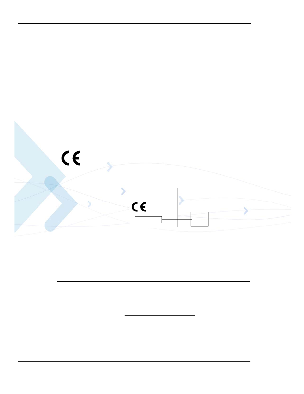
European Union Directives Conformance Statement
Hereby, Motorola declares that this product is in compliance with
• The essential requirements and other relevant provisions of
• All other relevant EU Directives
Directive 1999/5/EC
Product
Approval
Number
The above gives an example of a typical Product Approval Number.
You can view your product's Declaration of Conformity (DoC) to Directive 1999/5/EC (the
R&TTE Directive) at www.motorola.com/rtte - to find your DoC, enter the product Approval
Number from your product's label in the "Search" bar on the Web site.
Important: The following paragraphs must be addressed by the integrator to ensure their host is
in compliance to the H24 FCC grant and/or the FCC grant of the host device.
CFR 47 Part 15.19 specifies label requirements
The following text may be on the product, user's manual, or container.
This device complies with Part 15 of the FCC Rules. Operation is subject to the following two
conditions: (1) this device may not cause harmful interference, and (2) this device must accept
any interference received, including interference that may cause undesired operation.
6 H24 - Module Hardware Description November 15, 2009
Page 31

CFR 47 Part 15.21 Information to user
The user's manual or instruction manual for an intentional or unintentional radiator shall caution
the user that changes or modifications not expressly approved by the party responsible for
compliance could void the user's authority to operate the equipment. In cases where the manual is
provided only in a form other than paper, such as on a computer disk or over the Internet, the
information required by this section may be included in the manual in that alternative form,
provided the user can reasonably be expected to have the capability to access information in that
form.
CFR 47 Part 15.105 Information to the user
(b) For a Class B digital device or peripheral, the instructions furnished the user shall include the
following or similar statement, placed in a prominent location in the text of the manual:
Note: This equipment has been tested and found to comply with the limits for a Class B digital
device, pursuant to Part 15 of the FCC Rules. These limits are designed to provide
reasonable protection against harmful interference in a residential installation. This
equipment generates, uses and can radiate radio frequency energy and, if not installed and
used in accordance with the instructions, may cause harmful interference to radio
communications. However, there is no guarantee that interference will not occur in a
particular installation. If this equipment does cause harmful interference to radio or
television reception, which can be determined by turning the equipment off and on, the
user is encouraged to try to correct the interference by one or more of the following
measures:
- Reorient or relocate the receiving antenna.
- Increase the separation between the equipment and receiver.
- Connect the equipment into an outlet on a circuit different from that to which the
receiver is connected.
- Consult the dealer or an experienced radio/TV technician for help.
November 15, 2009 H24 - Module Hardware Description 7
Page 32

Regulatory Approvals
8 H24 - Module Hardware Description November 15, 2009
Page 33
Chapter 2: Hardware Interface Description
The following paragraphs describe in details the hardware requirements for properly interfacing
and operating the H24 module.
Architecture Overview
Figure 2-1 below illustrates the primary functional components of the H24.
Figure 2-1: H24 Block Diagram
November 15, 2009 H24 - Module Hardware Description 9
Page 34

Architecture Overview
The H24 consists of the following blocks:
Digital Block
• Micro-controller Unit (MCU) for system and user code execution.
• Digital Signal Processor (DSP) for voice and data processing.
• Serial communications interfaces.
• Digital audio (PCM) bus interface.
• General purpose IO signals.
Analog Block
• USB driver interface
• UART1
• UART2
• I2C
• SIM card
• Power Management IC (PMIC).
• Internal regulators
• 1 external regulator for customer use
• Analog audio interface management.
• Speaker, microphone
• Alert speaker
• Headset
• General purpose and dedicated A/D signals.
• A/D
• Voltage sensor
• Temperature sensor
• Real Time Clock (RTC) subsystem.
10 H24 - Module Hardware Description November 15, 2009
Page 35
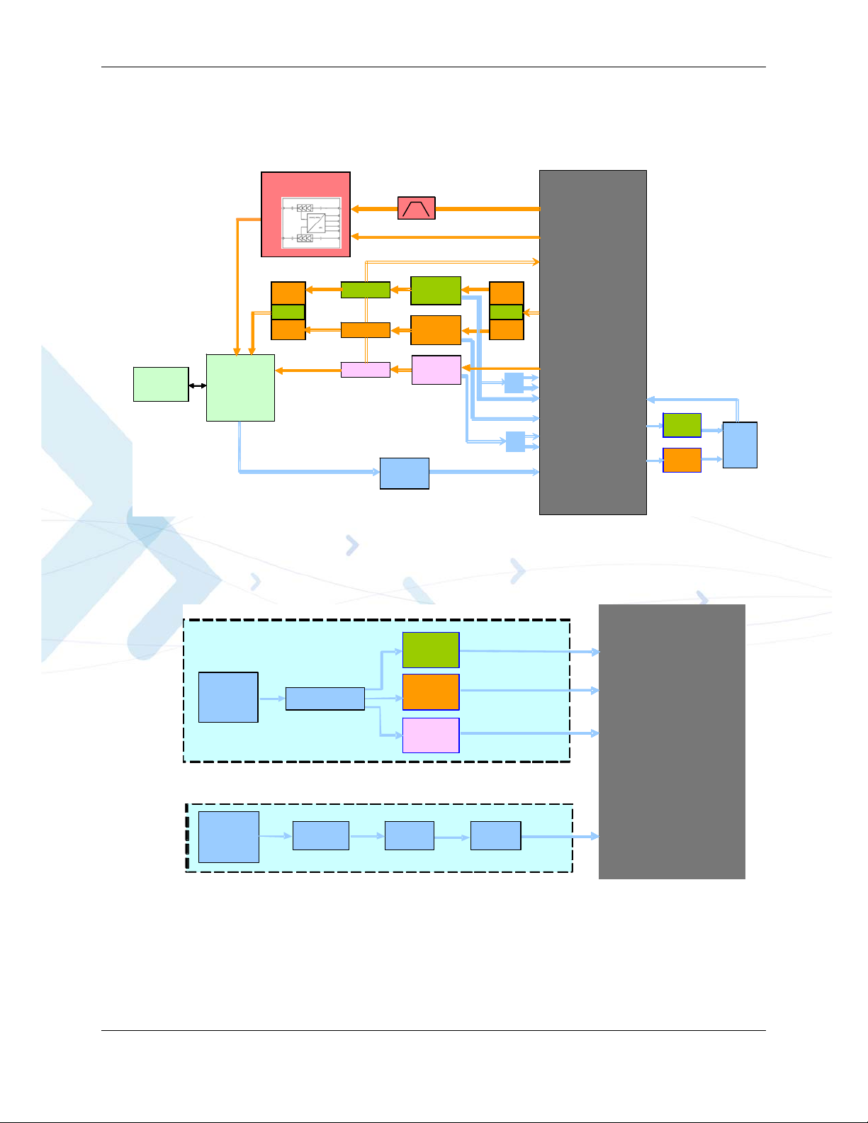
Chapter 2: Hardware Interface Description
RTR6285
XCVR
RF
SWITCH
SP8T
MAI N
CONN.
MMCX
COUPLER
PA WCDMA
B1- 2100
(U21)
GSM RX
QUAD
SAW
RF
SWITCH
Rx B PF
(WCDMA
B1 2100)
Rx B PF
(WCDMA
B2 1900)
PA WCDMA
B2- 1900
(U1)
PA WCD M A
B5-850
(U8)
COUPLER
COUPLER
SP DT
Qu ad - b a n d
GSM PA (U4)
B
CELL/GSM
DCS/PCS
1900
2100
2100/1900
850
SPDT
850
RTR6285
XCVR
RF
SWITCH
SP8T
MAI N
CONN.
MMCX
COUPLER
PA WCDMA
B1 / B4
(U21)
GSM RX
QUAD
SAW
RF
SWITCH
Rx B PF
(WCDMA
B1 2100)
Rx B PF
(WCDMA
B2 1900)
RF
SWITCH
Rx B PF
(WCDMA
B1 2100)
RF
SWITCH
Rx B PF
(WCDMA
B1 2100)
Rx B PF
PA WCDMA
B2- 1900
(U1)
PA WCD M A
B5-850
(U8)
COUPLER
COUPLER
SP DT
Qu ad - b a n d
GSM PA (U4)
Qu ad - b a n d
GSM PA (U4)
Qu ad - b a n d
GSM PA (U4)
BB
CELL/GSM
DCS/PCS
1900
2100
2100/1900/1700
850
SPDT
850
B
1700
RTR6285
XCVR
RF
SWITCH
SP8T
MAI N
CONN.
MMCX
COUPLER
PA WCDMA
B1- 2100
(U21)
GSM RX
QUAD
SAW
RF
SWITCH
Rx B PF
(WCDMA
B1 2100)
Rx B PF
(WCDMA
B2 1900)
PA WCDMA
B2- 1900
(U1)
PA WCD M A
B5-850
(U8)
COUPLER
COUPLER
SP DT
Qu ad - b a n d
GSM PA (U4)
B
CELL/GSM
DCS/PCS
1900
2100
2100/1900
850
SPDT
850
RTR6285
XCVR
RF
SWITCH
SP8T
MAI N
CONN.
MMCX
COUPLER
PA WCDMA
B1 / B4
(U21)
GSM RX
QUAD
SAW
RF
SWITCH
Rx B PF
(WCDMA
B1 2100)
Rx B PF
(WCDMA
B2 1900)
RF
SWITCH
Rx B PF
(WCDMA
B1 2100)
RF
SWITCH
Rx B PF
(WCDMA
B1 2100)
Rx B PF
PA WCDMA
B2- 1900
(U1)
PA WCD M A
B5-850
(U8)
COUPLER
COUPLER
SP DT
Qu ad - b a n d
GSM PA (U4)
Qu ad - b a n d
GSM PA (U4)
Qu ad - b a n d
GSM PA (U4)
BB
CELL/GSM
DCS/PCS
1900
2100
2100/1900/1700
850
SPDT
850
B
1700
RTR6285
XCVR
DIV
CONN.
UFL
Rx BPF
(WCDMA
B5 850)
Rx BPF
(WCDMA
B2 1900)
Rx BPF
(WCDMA
B1 2100)
RX DIVERSITY
INPUTS
RF SWITCH
DIVERSITY
GPS
CONN.
UFL
GPS
BPF
GPS
BPF
LNA
GPS
RTR6285
XCVR
DIV
CONN.
UFL
Rx BPF
(WCDMA
B5 850)
Rx BPF
(WCDMA
B2 1900)
Rx BPF
(WCDMA
B1 2100)
RX DIVERSITY
INPUTS
RF SWITCH
DIVERSITY
GPS
CONN.
UFL
GPS
BPF
GPS
BPF
LNA
GPS
RTR6285
XCVR
DIV
CONN.
UFL
Rx BPF
(WCDMA
B5 850)
Rx BPF
(WCDMA
B2 1900)
Rx BPF
(WCDMA
B1 / B4)
RX DIVERSITY
INPUTS
RF SWITCH
DIVERSITY
GPS
CONN.
UFL
GPS
BPF
GPS
BPF
LNA
GPS
RTR6285
XCVR
DIV
CONN.
UFL
Rx BPF
(WCDMA
B5 850)
Rx BPF
(WCDMA
B2 1900)
Rx BPF
(WCDMA
B1 2100)
RX DIVERSITY
INPUTS
RF SWITCH
DIVERSITY
GPS
CONN.
UFL
GPS
BPF
GPS
BPF
LNA
GPS
RTR6285
XCVR
DIV
CONN.
UFL
Rx BPF
(WCDMA
B5 850)
Rx BPF
(WCDMA
B2 1900)
Rx BPF
(WCDMA
B1 2100)
RX DIVERSITY
INPUTS
RF SWITCH
DIVERSITY
GPS
CONN.
UFL
GPS
BPF
GPS
BPF
LNA
GPS
RTR6285
XCVR
DIV
CONN.
UFL
Rx BPF
(WCDMA
B5 850)
Rx BPF
(WCDMA
B2 1900)
Rx BPF
(WCDMA
B1 / B4)
RX DIVERSITY
INPUTS
RF SWITCH
DIVERSITY
GPS
CONN.
UFL
GPS
BPF
GPS
BPF
LNA
GPS
RF Transceiver Block
Figure 2-2 and Figure 2-3 give a detailed RF block diagram.
Figure 2-2: GSM and WCDMA Main Connector Block Diagram
Figure 2-3: WCDMA Diversity Circuitry Block Diagram
Note: GPS is not supported in the current version.
November 15, 2009 H24 - Module Hardware Description 11
Page 36

Architecture Overview
WCDMA Transceiver
• RTR6285 includes: modulator, receiver, LNAs, Mixers, VCOs, I/Q outputs and buffers for
• Three RF Power Amplifiers for B1-2100 or B4-1700, B2-1900 & B5 - 850.
• Three couplers for feedback into the Modulator for each band.
• RF Switch SP9T for selecting corrected path to and from main MMCX connector.
• Receive path is inside PA via internal duplexer into the RTR.
• Internal LNAs for all WCDMA bands inside RTR
• External switch, RF SPDT, from WB1900 & WB2100 LNA's output into one receiver's
• Diversity path: From Diversity UFL connector via SP3T into SAW filter for
all WCDMA bands.
differential input.
WB2100/W1700, WB1900 & WB850 fed into secondary receivers inputs inside the RTR.
12 H24 - Module Hardware Description November 15, 2009
Page 37

Operating Modes
H24 incorporates several operating modes. Each operating mode is different in the active features
and interfaces.
Table 2-1 summarizes the general characteristics of the H24 operating modes and provides
general guidelines for operation.
Chapter 2: Hardware Interface Description
Table 2-1:
Mode Description Features
Not Powered VCC supply is disconnected. The H24 is Off.
Off Mode Valid VCC supply.
RESET_N signal is enabled (low).
Idle Mode RESET_N signal is disabled (high).
CTS_N and DSR_N signals are enabled
(low).
Sleep Mode RESET_N signal is high.
CTS_N signal is disabled.
CSD call or
GPRS/EGPRS
data
CSD call or
WCDMA/HSPA
data
RESET_N signal is high.
TXEN_N signal is toggling.
RESET_N signal is high.
TXEN_N signal is toggling.
H24 Operating Modes
Any signals connected to the interface connector must be set low or tri-state.
The H24 Interfaces are Off. Only the internal RTC timer is operating. Any signals
connected to the interface connector must be
set low or tri-stated.
The H24 is fully active, registered to the
GSM network and ready to communicate.
This is the default power-up mode.
The H24 is in low power mode.
The application interfaces are disabled, but,
H24 continues to monitor the GSM network.
A GSM voice or data call is in progress.When the call terminates, H24 returns
to the last operating state (Idle or Sleep).
A GSM voice or data call is in progress.
When the call terminates, H24 returns to the
last operating state (Idle or Sleep).
November 15, 2009 H24 - Module Hardware Description 13
Page 38

Power Supply
Power Supply
The H24 power supply must be a single external DC voltage source of 3.3V to 4.2V. The power
supply must be able to sustain the voltage level during a GSM transmit burst current surge, which
may reach 2.0A.
The H24 interface connector has 8 contacts for the main power supply, as described in Table 2-2.
All these contacts must be used for proper operation.
Table 2-2:
Power Supply Signals
Pin # Signal Name Description
1-4 GND Main ground connection for H24
module.
5-8 VCC DC supply input for H24 module.
= 3.3 V to 4.2 V
V
IN
= 2 A during transmit
I
MAX
bursts
Maximum rise time: 8mS
AC ripple: +/-3%
Important: Do not operate the H24 out of its electrical or environmental limits. Refer to the
specifications chapter for details of these limits.
Important: The H24 does not incorporate a hard reset capability. The user should implement a
power removal mechanism for hard resetting the unit when needed. This action will
be performed with care as it could cause damage to the H24.
Power Supply Design
Special care must be taken when designing the power supply of the H24. The single external DC
power source indirectly supplies all the digital and analog interfaces, but also directly supplies the
RF power amplifier (PA). Therefore, any degradation in the power supply performance, due to
losses, noises or transients, will directly affect the H24 performance.
The burst-mode operation of the GSM transmission and reception, draws instantaneous current
surges from the power supply, which causes temporary voltage drops of the power supply level.
The transmission bursts consume the most instantaneous current, and therefore cause the largest
voltage drop. If the voltage drops are not minimized, the frequent voltage fluctuations may
degrade the H24 performance.
14 H24 - Module Hardware Description November 15, 2009
Page 39

Chapter 2: Hardware Interface Description
Figure 2-4 illustrates the power supply behavior during GSM transmission.
Figure 2-4: Transmission Power Drops
Note: 1 TX slot is shown.
It is recommended that the voltage drops during a transmit burst will not exceed 300mV,
measured on the H24 interface connector. In any case, the H24 supply input must not drop below
the minimum operating level during a transmit burst. Dropping below the minimum operating
level may result in a low voltage detection, which will initiate an automatic power-off.
To minimize the losses and transients on the power supply lines, it is recommended to follow
these guidelines:
• Use a 1000 uF, or greater, low ESR capacitor on the H24 supply inputs. The capacitor should
be located as near to the H24 interface connector as possible.
• Use low impedance power source, cabling and board routing.
• Use cabling and routing as short as possible.
• Filter the H24 supply lines using filtering capacitors, as described in Table 2-3.
Table 2-3:
Capacitor Usage Description
1000 uF GSM Transmit current
10 nF, 100 nF Digital switching noise
8.2 pF, 10 pF 1800/1900/2100/1700
Recommended Power Supply Filtering
Minimizes power supply
serge
MHz bands
losses during transmit
bursts- no more than
200mV.
Use maximum possible
value.
Filters digital logic noises
from clocks and data sources.
Filters transmission EMI.
33 pF, 39 pF 850/900 MHz bands
November 15, 2009 H24 - Module Hardware Description 15
Filters transmission EMI.
Page 40
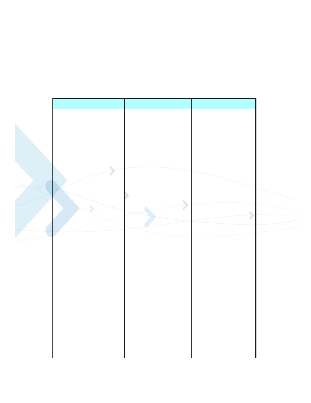
Power Supply
Current Consumption
The table below specify typical H24 current consumption ratings in various operating modes. The
current ratings refer to the overall H24 current consumption over the VCC supply.
Note: H24 was tested at 25°C, voltage level was 4V.
Idle mode measurments were taken without USB cable connected.
Table 2-4: H24 Current Ratings
Parameter Description Conditions Min Typ Max Unit
I
OFF
I
IDLE
I
SLEEP
I
GSM-RMS
RTC mode 40 50 µA
Idle mode 22 mA
Low power mode DRx 2
GSM850 PCL 5
EGSM900 PCL 5
GSM voice 1 TX slot
1 Rx slot
DCS1800 PCL 0
PCS1900 PCL 0
GSM850 PCL 5
5
9
10
15
19
10
15
19
5
10
15
5
10
15
10
15
19
2.95
1.82
1.42
328
215
165
152
310
213
161
150
250
201
159
152
271
187
161
153
577
456
265
217
mA
mA
EGSM900 PCL 5
10
15
I
GPRS-RMS
16 H24 - Module Hardware Description November 15, 2009
GPRS Class 12 4 TX slot
1 Rx slot
DCS1800 PCL 0
PCS1900 PCL 0
19
5
10
15
5
10
15
611
485
278
222
401
322
237
210
451
354
247
213
mA
Page 41

Chapter 2: Hardware Interface Description
Table 2-4: H24 Current Ratings (Cont.)
Parameter Description Conditions Min Typ Max Unit
I
EGPRS-RMS
I
GSM-MAX
EGPRS Class 12 4 TX slot
1 Rx slot
Peak current
During TX slot
GSM850 PCL 8
EGSM900 PCL 8
DCS1800 PCL 2
PCS1900 PCL 2
GSM850 PCL 5
GSM900 PCL 5
DCS1800 PCL 0
14
19
14
19
9
15
9
15
10
15
19
10
15
19
5
10
15
369
227
219
389
231
222
317
244
211
346
257
212
1873
853
438
331
1667
886
459
335
1126
562
373
315
mA
mA
I
WCDMA-RMS
WCDMA
PCS1900 PCL 0
5
10
15
WCDMA850 24dBm
0dBm
-24dBm
-50dBm
WCDMA1900 24dBm
0dBm
-24dBm
-50dBm
WCDMA2100 24dBm
0dBm
-24dBm
-50dBm
WCDMA1700 24dBm
0dBm
-24dBm
-50dBm
1302
637
400
327
512
172
168
167
537
146
135
133
608
217
211
209
TBD
TBD
TBD
TBD
mA
November 15, 2009 H24 - Module Hardware Description 17
Page 42

Power On/Off Operation
Power On/Off Operation
The H24 power on and off process includes two primary phases, which are indicated at the
interface connector by the hardware output signals RESET_N and CTS_N.
The RESET_N signal indicates whether H24 is powered on or off.
When this signal is enabled (low), H24 is powered-off. When it is disabled (high), H24 is
powered-on.
The CTS_N signal complys with RS-232 standard. When this signal is high, the H24 serial
interface is disabled. When it is low, the serial interface is enabled, and H24 is ready to
communicate.
Turning the H24 On
When the H24 power supply is stable above the minimum operating level and H24 is powered
off, only the internal RTC timer is active.
When H24 is turned on, by any of the methods described below, it will first perform an automatic
internal system-test, during which basic functions are verified. The system-test duration is
typically 3 seconds (Depends on network coverage). When the system-test has completed H24
resumes normal operation.
During the internal system-test process H24 may toggle several interface signals, which are
visible to the application. These signals do not represent any valid state or data, and should be
ignored by the customer application until the system-test has completed.
Power Supply Turn-on
When the H24 is powered for the first time, it is always switched on. In case the valid reason
detected (IGN, ON_N activation) it will stayed on, otherwise it will switch off.
The ON_N and IGN signals will be active and responding only after the power supply to the H24
is stable above the minimum operating level. Therefore, the ON_N and IGN signals must not be
used for at least 100 milliseconds after applying power to H24.
Turning the H24 On Using ON_N
The ON_N input signal is set high by an internal pull-up resistor whenever a power supply is
applied to H24. Therefore, it is recommended to operate this signal using an open collector/drain
circuit connection.
Asserting the ON_N signal low for a minimum of 500 milliseconds (0.5 seconds) and a maximum
of 1.5 seconds will cause the H24 to turn-on.
Asserting the ON_N signal low for more than 1.5 seconds may cause the H24 to interpret the
signal as a power-off command, and turn off immediately after turning on.
18 H24 - Module Hardware Description November 15, 2009
Page 43

Chapter 2: Hardware Interface Description
Turning the H24 On Using IGN
The IGN input signal must be set low when not used. To turn on H24, this signal must be asserted
high. The IGN signal must remain high for the duration of the H24 operation. H24 powers down
when the IGN signal is returned to its low state.
Turning the H24 Off
There are several ways to turn the H24 off:
• Asserting the ON_N signal low for a minimum of 2 seconds.
• Setting the IGN signal low.
• Low power automatic shut down.
• AT command.
• Voltage exceeds 4.5V.
• Temperature at PMIC exceeds 125°C.
Turning the H24 Off Using ON_N
The ON_N signal is set high using an internal pull up resistor when power is applied to H24.
Asserting the ON_N signal low for a minimum of 2 seconds will turn H24 off. This will initiate a
normal power-off process, which includes disabling of all applications interfaces (UART, SIM
card, audio, etc.) and closing the network connection.
Turning the H24 Off Using IGN
The IGN signal may be used to power off H24 only if it was also used to power it on. When the
IGN signal is set low, H24 will turn off. This will initiate a normal power-off process, which
includes disabling of all applications interfaces (UART, SIM card, audio, etc.) and closing the
network connection.
The IGN signal will not power off H24 before 30 seconds have elapsed since H24 was
powered-on. This delay mechanism is implemented to protect H24 from unexpected transients on
the IGN line during power up, particularly when applying vehicle cranking waveforms.
Power Loss shut down
A low power shut down occurs when H24 senses the external power supply is below the minimal
operating limit. The module will respond by powering down automatically without notice.
This form of power-down is not recommended for regular use since the unexpected power loss
may result in loss of data.
Turning the H24 Off Using AT+MPWRDN
The AT+MPWRDN command initiates a H24 power down (even if the H24 was powered on by
IGN). This command emulates the ON_N signal operation for power off.
November 15, 2009 H24 - Module Hardware Description 19
Page 44

Low Power Mode
Low Power Mode
The H24 incorporates an optional low power mode, called Sleep Mode, in which it operates in
minimum functionality, and therefore draws significantly less current. During low power mode
the H24 network connection is not lost. H24 continues to monitor the GSM network constantly
for any incoming calls or data.
During low power mode, most of the H24 interface signals are inactive and are kept in their
previous state, prior to activating low power mode. To save power, the H24 internal Main clock
and some of its circuits are shut down, and therefore serial communications is limited.
Activating Low Power Mode
UART:
By default, the H24 powers on in Idle mode. In this mode the H24 interfaces and features are
functional and the module is fully active.
Low power mode is controlled by the AT+MSLEEP & ATS24 commands.
The command AT+MSLEEP=1 enable Sleep Mode (AT+MSLEEP=0 disable Sleep Mode).
The value of S24 command determines the inactive state duration required by H24, in seconds,
after which H24 will enter sleep mode.
For example:
ATS24 = 1 activates low power mode after 1 second of UART inactivity.
ATS24 = 5 activates low power mode after 5 seconds of UART inactivity.
Note: ATS24=0 will not disable sleep mode at H24.
AT+MSLEEP = 1 Enable low power mode.
AT+MSLEEP = 0 Disable low power mode (default).
Important: H24 will not enter low power mode in any case when there is data present on the
serial interface.Also when any network (GSM/UMTS ) activity (e.g. incoming
voice call, data session) or an internal system task is running. Only when processing
of any external or internal system task has completed, if AT+MSLEEP=1 and H24
UART is inactive for the duration of ATS24, H24 will enter low power mode.
USB
:
Any transaction to the USB will wake up the H24 provided the user USB stack supports
suspend/resume mechanism. In case such mechanism is not supported the user will not be able set
the H24 at sleep mode.
In case of resume event the SW will be responsible to all the needed configurations (endpoints
etc.) to maintain the link. In case the host USB protocols stack doesn't support resume suspend
mechanism the USB module in the H24 will not go to sleep hence the entire H24 will remain
active as long as the USB cable is connected.
Remote wake up is supported.
CTS signal conforms RS-232 standard at this mode.
20 H24 - Module Hardware Description November 15, 2009
Page 45
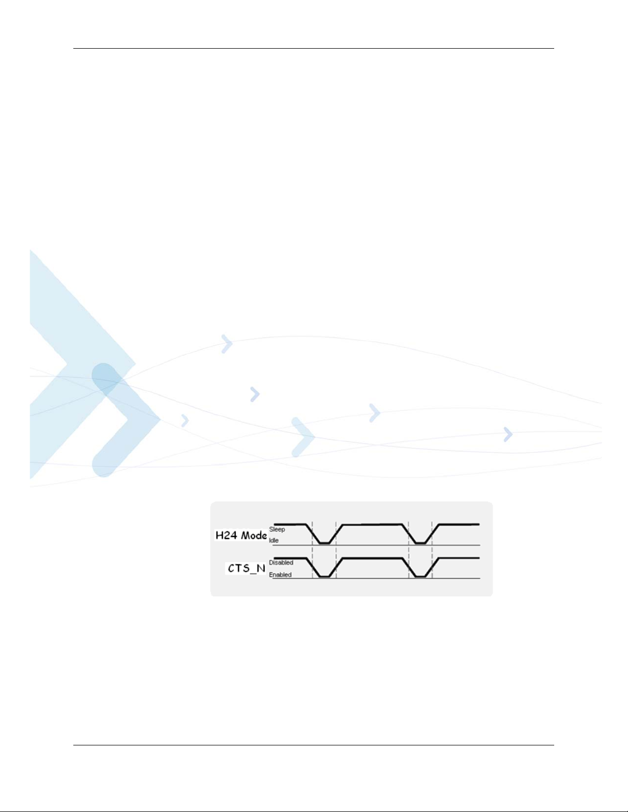
Chapter 2: Hardware Interface Description
Serial Interface During Low Power Mode
During low power mode the H24 serial interfaces are disabled. This is indicated by the CTS_N
signal high state (if hardware flow control is set by AT+IFC=2, 2 (or AT&K4) and CTS control is
set by AT+MSCTS=1 command).
The H24 wakes up periodically from low power mode to listen to paging channel of the
GSM/WCDMA networks for any incoming calls or data. After this short paging is completed,
H24 returns to low power mode. During this short awake period, the serial interfaces are enabled
and communications with the module is possible (if both AT+IFC=2, 2 (or AT&K4) and
AT+MSCTS=1 commands are in use).
The CTS_N signal is alternately enabled and disabled synchronously with the network paging
cycle. CTS_N is enabled whenever H24 awakes to page the network. This indicates the H24
serial interfaces are active (see Figure 2-5).
When using AT+IFC=2, 2 the Heaper Terminal should be set to flow control - HW.
When using AT+IFC=0, 0 the Heaper Terminal should be set to flow control - None.
Need to disconnect and connect to Heaper terminal for the new setup to be active.
RS232 cable hot swap is supported and insert cable will wake up the H24.
WAKEUP_IN line pin 16 (on 70 pin connector) should override any sleep condition and will
prevent H24 from enter sleep mode.
In case user is working with UART and enables HW flow control, it is advised that the user will
plan his system to wake up H24 also using the WAKEUP_IN HW line.
If the following conditions become true the user will be able to wake H24 only through
WAKEUP_IN line (or just return to work with folow control = None); and will not be able to
wake H24 through RX activity (sending data):
• Sleep mode over UART enabled
• UART HW flow control enabled
• Airplane mode enabled (AT+CFUN=0 or AT+CFUN=4).
In this case there is no DRX and CTS is not rising.
Figure 2-5: CTS Signal During Sleep Mode
The periodical enabling and disabling of the CTS_N signal during low power mode can be
controlled by the AT+MSCTS command.
Setting AT+MSCTS=0 permanently disables the serial interface during low power mode, even
during a network page by H24. The CTS_N signal is disabled, and therefore the serial interfaces
are blocked.
November 15, 2009 H24 - Module Hardware Description 21
Page 46

Low Power Mode
Terminating Low Power Mode
Terminating the low power mode, or wake-up, is defined as the transition of the H24 operating
state from Sleep mode to Idle mode. There are several ways (using UART CTS_N signal,
WKUPI_N line or UART RX line interrupt) to wake-up H24 from low power mode as described
below.
Important: During power saving mode the H24 internal clocks and circuits are disabled, in
order to minimize power consumption. When terminating the power saving mode,
and switching to Idle mode, H24 requires a minimal delay time to reactivate and
stabilize its internal circuits before it can respond to application data.
This delay is typically of 100 milliseconds, and is also indicated by the CTS_N
signal inactive (high) state. The delay guarantees that data on the serial interface is
not lost or misinterpreted.
Temporary Termination of Low Power Mode
The WKUPI_N signal is an active low input that is set high by default. By asserting this signal
low the application can wake-up H24 from low power mode and switch to idle mode.
Low power mode may be terminated temporarily by several sources, some of which are user
initiated and others are initiated by the system.
Using the WKUPI_N signal to wake UART from Sleep Mode
The WKUPI_N signal is an active low input, that is set high by default. By asserting this signal
low the application can wake-up H24 from low power mode and switch to Idle mode.
H24 will remain in idle mode, awake and fully active, as long as WKUPI_N signal remains low.
When this signal is disabled and set high again, H24 will return to Sleep mode automatically,
according to the ATS24 settings.
The WKUPI_N signal is the recommended method to temporarily wake-up H24 from low power
mode. It provides the application full control of the H24 operating mode and guarantees that data
on the serial interface will not be lost or misinterpreted.
The WKUPI_N signal can be used to wake up H24 from low power mode. If the serial interface
has been controlled by the AT+IFC=1,1 (or AT&K4) command, the application can work in
Hardware Flow Control accumulate the data in its buffer and send it to the module when the CTS
is Enabled. (Note: this method of operation works without using AT+MSCTS=0 command).
Incoming Network Data
During low power mode, H24 continues monitoring the network (GSM or UMTS) for any
incoming data, message or voice calls.
When H24 receives an indication from the network that an incoming voice call, message or data
is available, it automatically wakes up from low power mode to alert the application. When H24
has completed to process all the tasks related to the incoming data, it will automatically return to
low power mode according to the ATS24 settings.
Depending on the type of network indication and the application settings, H24 may operate in
several methods, which are configurable by AT commands, to alert the application of the
incoming data:
22 H24 - Module Hardware Description November 15, 2009
Page 47
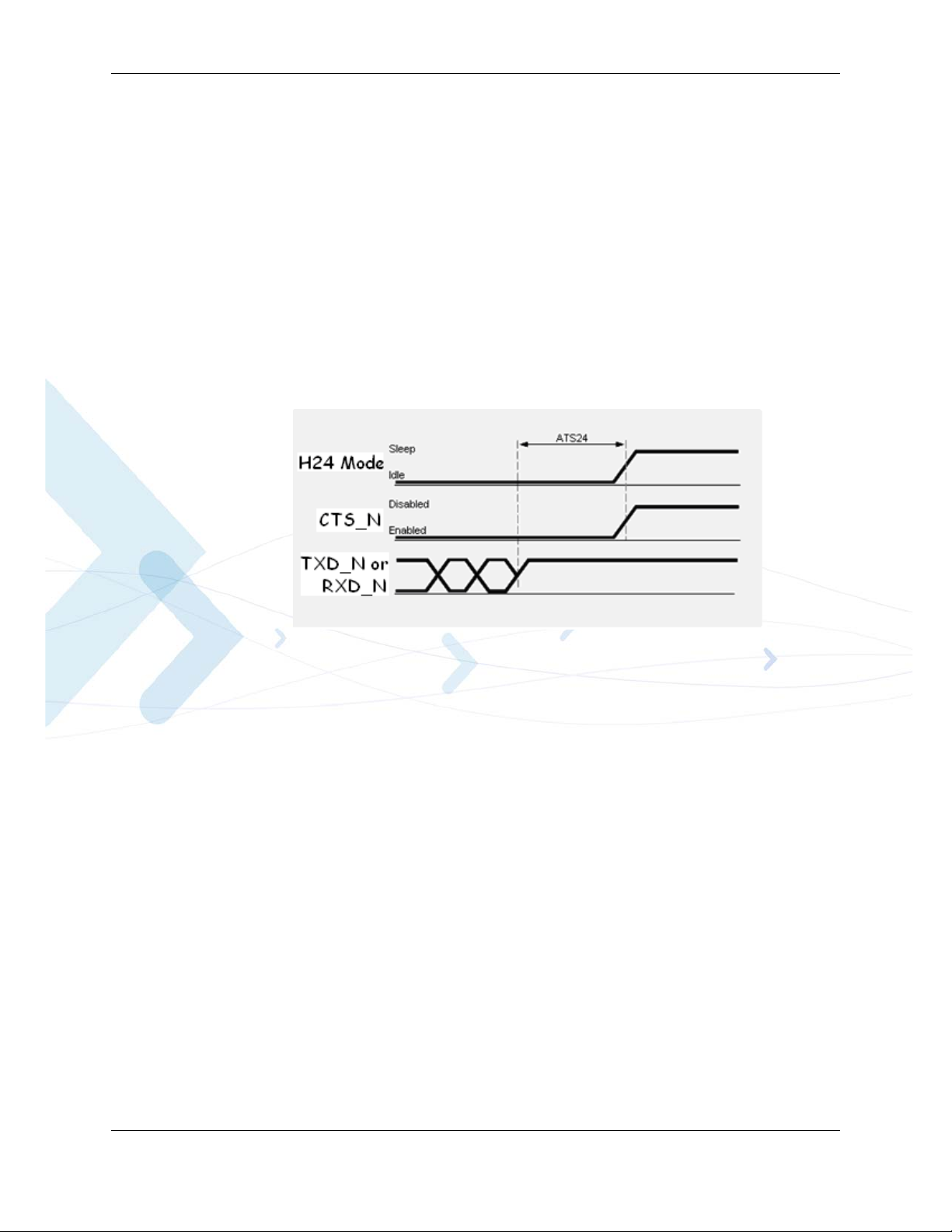
Chapter 2: Hardware Interface Description
• Enable the WKUPO_N signal to wake-up the application from low power by setting ATS100
to value bigger then zero. ATS102 can be 0 but is 30ms by default for example ATS102=30
will start WKUPO_N signal 30 millisecond before data send out from UART to Host.
• Send data to the application over the serial interface.
• Enable the serial interface's Ring Indicator (RI_N) signal.
Data on the Serial interface
While H24 is temporarily awake in Idle mode, data may be transmitted on the serial interface. In
case data is being transmitted in any direction, H24 will not return to low power mode. This is
regardless of the original wake-up reason or source. H24 will remain awake while data is
transferred.
Only when the serial interface transfer is completed and the data has been processed, H24 will
return to low power mode automatically, according to the ATS24 settings (see Figure 2-6).
Figure 2-6: Serial Interface Data
UART and USB Exiting of Low Power Mode
Enable/Disable Low Power Mode
The H24 low power mode is enabled and disabled by the AT+MSLEEP command.
To permanently terminate the H24 low power mode, the +MSLEEP=0 command must be used.
H24 will not return to low power mode until an AT+MSLEEP=1 commands is set again.
This command can be sent only when the serial interface is active.
UART Exiting of Low Power Mode
In case the serial interface is disabled, Hardware Flow control is OFF and WKUP_I is not used, it
must first be activated before sending this command. To reactivate the serial interface, a
temporary termination of the low power mode is required, by sending AT command that will
catch by the RX line interrupt service routine and will use to wake up the module (The execution
of the first command after exit Sleep Mode by RX interrupt is not guarantied.
USB Exiting of Low Power Mode
Handled by suspend/resume mechanism.
November 15, 2009 H24 - Module Hardware Description 23
Page 48

Real Time Clock
Real Time Clock
H24 incorporates a Real Time Clock (RTC) mechanism that performs time keeping. The RTC
subsystem is embedded in the PMIC and operates in all of the H24 operating modes (Off, Idle,
Sleep), as long as power is supplied above the minimum operating level.
The H24 time and date can be set using the following methods:
• Automatically retrieved from the GSM network.
In case H24 is operated in a GSM network that supports automatic time zone updating, it will
update the RTC with the local time and date upon connection to the network. The RTC will
continue to keep the time from that point.
• Using the AT+CCLK command.
Setting the time and date manually by this AT commands overrides the automatic network
update.
Once the time and date are manually updated, the RTC timer will keep the time and date
synchronized regardless of the H24 operating state.
When the power supply is disconnected from H24, the RTC timer will reset and the current time
and date will be lost. On the next H24 power-up the time and date will need to be set again
automatically or manually.
Nevertheless, there is ability to keep the RTC working while main power supply is off.
This can be done by supplying the RTC an external power of 3V to a dedicated pin in the
microprocessor.
This dedicated pin is called Vcoin.
When the main power supply is off and Vcoin is active, the RTC is still working.
When power supply is off, no Vcoin applied, the RTC will work only for 2 sec, and will turn
"off".
24 H24 - Module Hardware Description November 15, 2009
Page 49

Serial Interfaces
H24 includes three completely independent serial communications interfaces, which may be used
by the application for several purposes.
Primary UART (UART1)
The H24 primary UART is a standard 8-signal bus. The primary UART is used for all the
communications with H24 - AT commands interface, GPRS/EGPRS data and CSD data,
programming and software upgrades.
The UART signals are active low CMOS level signals. For standard RS232 communications with
a PC, an external transceiver is required.
H24 is defined as a DCE device, and the user application is defined as the DTE device. These
definitions apply for the UART signals naming conventions, and the direction of data flow, as
described in Figure 2-7.
Chapter 2: Hardware Interface Description
Figure 2-7: UART1 Interface Signals
The H24 primary UART supports maximum data rate of up to 4 Mbps interface and up to 230
kbps for data services using the UART1 interface.
All flow control handshakes are supported: hardware, software, or none.
Parity bit and Stop bit definitions are also supported.
The UART default port configuration is 8 data bits, 1 stop bit and no parity, with hardware flow
control.
USB Interface
H24 incorporates a standard Universal Serial Bus (USB) interface.
The H24 USB electrical interface and protocol conform to the USB 2.0 high-speed specifications.
H24 is defined as a USB device on the USB bus and does not support hub or host functionality.
November 15, 2009 H24 - Module Hardware Description 25
Page 50

Serial Interfaces
USB may be used for standard communications with H24, as done through the UART interface.
The USB interface signals are shown in Figure 2-8.
Figure 2-8: USB Interface Signals
UID determines the USB mode configuration: Host or Client (Client mode is supported).
Note: Do not connect USB_ID pin (pin 45).
Important: When layouting USB signals: Run HS_D_P/M as diff pair with equal length , to
maintain 100-Ohms diff/50-Ohms single-ended.
26 H24 - Module Hardware Description November 15, 2009
Page 51

SIM Interface
The H24 incorporates a SIM interface, which conforms to the GSM 11.11 and GSM 11.12
standards, that are based on the ISO/IEC 7816 standard. These standards define the electrical,
signaling and protocol specifications of a GSM SIM card.
H24 does not incorporate an on-board SIM card tray for SIM placement. The SIM must be
located on the user application board, external to the H24. The H24 SIM interface includes all the
necessary signals, which are routed to the interface connector, for a direct and complete
connection to an external SIM.
H24 supports dynamic detection of the SIM card, through a dedicated SIM detection signal. H24
will detect a SIM card insertion or removal upon power up or during operation by the transitions
on the SIM_PD_N signal.
Some of the H24 models incorporates eSIM (embedded SIM). Refer to “Embedded SIM” on
page 28.
External SIM Connection
Table 2-5 details the SIM interface signals.
Chapter 2: Hardware Interface Description
Table 2-5: SIM Interface Signals
Connected
to 70 pin
44 SIM_RST_N N
46 SIM_CLK N
48 SIM_VCC N
50 SIM_PD_N Y
52 SIM_DIO N
H24 Interruptible
SIM Design Guidelines
The SIM interface and signals design is extremely important for proper operation of H24 and the
SIM card. There are several design guidelines that must be followed to achieve a robust and
stable design that meets the required standards and regulations.
• Using the SIM detection signal, SIM_PD_N, is mandatory in case the SIM card is accessible
to the user and may be removed during H24 operation. To avoid any damage to the SIM or
H24, the SIM interface signals must be deactivated before the SIM card contacts are
mechanically removed from the SIM tray contacts. Therefore, the SIM_PD_N detection
signal must be disabled before the SIM is removed from its tray.
• The SIM should be located, and its signals should be routed, away from any possible EMI
sources, such as the RF antenna and digital switching signals.
• The SIM interface signals length should not exceed 100 mm between the H24 interface
connector and the SIM tray. This is to meet with EMC regulations and improve signal
integrity.
November 15, 2009 H24 - Module Hardware Description 27
Page 52

SIM Interface
• To avoid crosstalk between the SIM clock and data signals (SIM_CLK and SIM_DIO), it is
recommended to rout them separately on the application board, and preferably isolated by a
surrounding ground plane.
• The SIM card signals should be protected from ESD using very low capacitance protective
elements (zener diodes, etc.).
• The H24 interface does not support SIM programming through the VPP signal. This signal
should not be connected to H24.
• SIM voltage level will not drop below 2.7V (1.6V for 1.8V SIM card) during hot insertion.
• It is recommended to add series termination at signals SIM CLK (100 Ohm) and the
SIM_DIO (56 Ohm) and bypass SIM_VCC with a 100nF cap.
Embedded SIM
The H24 newest feature is incorporating an Embedded SIM inside (depending on H24 model).
Embedded SIM (e.g. eSIM or chip SIM), is a secured micro controller IC, with the same pinout
interface, and the same operation as an external SIM card.
The eSIM main advantage is it robustness, making it an ideal solution for M2M applications.
Since an eSIM is actually an IC soldered on the H24, it can withstand wider temperature range
then a regular external SIM card that is usually made of plastic, and gets twisted and bowed at
high temperature, causing disconnection inside the SIM tray.
For the same reason, the eSIM is more durable to vibration then a regular external SIM card. Hard
vibration on an application with a SIM card socket may result in with an intermitted connection
between the SIM card socket and the SIM card.
Two signals are associated with the eSIM:
• SIM_PD_N: (pin 50) This signal must be set low for acknowledge the H24 that eSIM is
connected.
• Chip SIM reset: (pin 56) This pin is dedicated for reseting the eSIM. In case that the eSIM is
incorporated, short circuit this pin to pin 44 (SIM_RST_N).
28 H24 - Module Hardware Description November 15, 2009
Page 53

Audio Interface
The H24 audio interface supports several audio devices and operating modes.
The audio interface's operating modes, active devices, amplification levels and speech processing
algorithms are fully controlled by the host application, through advanced programming options
and a versatile AT commands set.
The H24 supports the following audio devices:
• Two single-ended/ Differential and mono analog microphone inputs for use in a variety of
modes.
• Differential mono analog speaker output.
• Differential mono analog alert output. (Amplified to 1W)
• Single-ended mono analog headset output.
• A digital serial interface using PCM coding.
All the above analog audio paths with the interface to the 70 pin connector are shown in
Figure 2-9.
Chapter 2: Hardware Interface Description
Figure 2-9: H24 Audio Interface
Handset Interface
Typical handset interfaces are shown in Figure 2-10. The earphone output pins are connected
directly to the handset's earphone with 2 bypass capacitors connected to ground. The capacitance
is selected de-pending on the design, typically less than 100 pF.
November 15, 2009 H24 - Module Hardware Description 29
Page 54

Audio Interface
The output power for the differential EAR1 output is typically 70 mW for a full-scale +3 dBm0
sine wave into a 32Ω speaker.
Both microphone pins require 2.2 k bias resistors and 0.1µF AC-coupling capacitors.
The positive microphone terminal is connected to the µC MICBIAS pin through one of the
2.2 kΩ resistors; this 1.8 V output provides 1 mA of bias current for the Microphone.
MICBIAS supports multiple microphones simultaneously up to 1 mA.
In case the user connect single-ended mic, he must connect it to pin 61 and short circuit pin 62 to
ground.
For gain levels, please refer to H24 AT Commands manual - 6802986C37.
Figure 2-10: Handset Interface
Headset Interface
The most basic handset configuration is shown in Figure 2-11. This configuration uses an
AC-coupled mono earphone interface and a standard single-ended microphone interface.
The output power for the single-ended HPH_L/HPH_R output is typically 21.6 mW per side for a
full-scale +3 dBm0 sine wave into a 15Ω speaker.
30 H24 - Module Hardware Description November 15, 2009
Page 55

Chapter 2: Hardware Interface Description
Few alternative earphone configurations are given in the following paragraphs. If the load
capacitance is greater than 100 pF due to earphones with different capacitive load used, a RC
shunt network (0.22µF and 22Ω) is recommended to prevent oscillations as shown in Figure 2-11.
Note: In case a differential mic is used, the negative node should be connected to pin 70.
Figure 2-1 1: Headset Interface
Interface to an External Speaker Amplifier
The power management device can also be used as a speaker amplifier. The power management
speaker driver output power is rated at 500 mW and can be adjust up to 1W. To use this feature as
an amplifier of an audio output, be sure to set the appropriate speaker driver analog and digital
gains, and set the analog high-pass filter corner at the resonant frequency of the far-field speaker
transducer (see Figure 2-12).
November 15, 2009 H24 - Module Hardware Description 31
Page 56
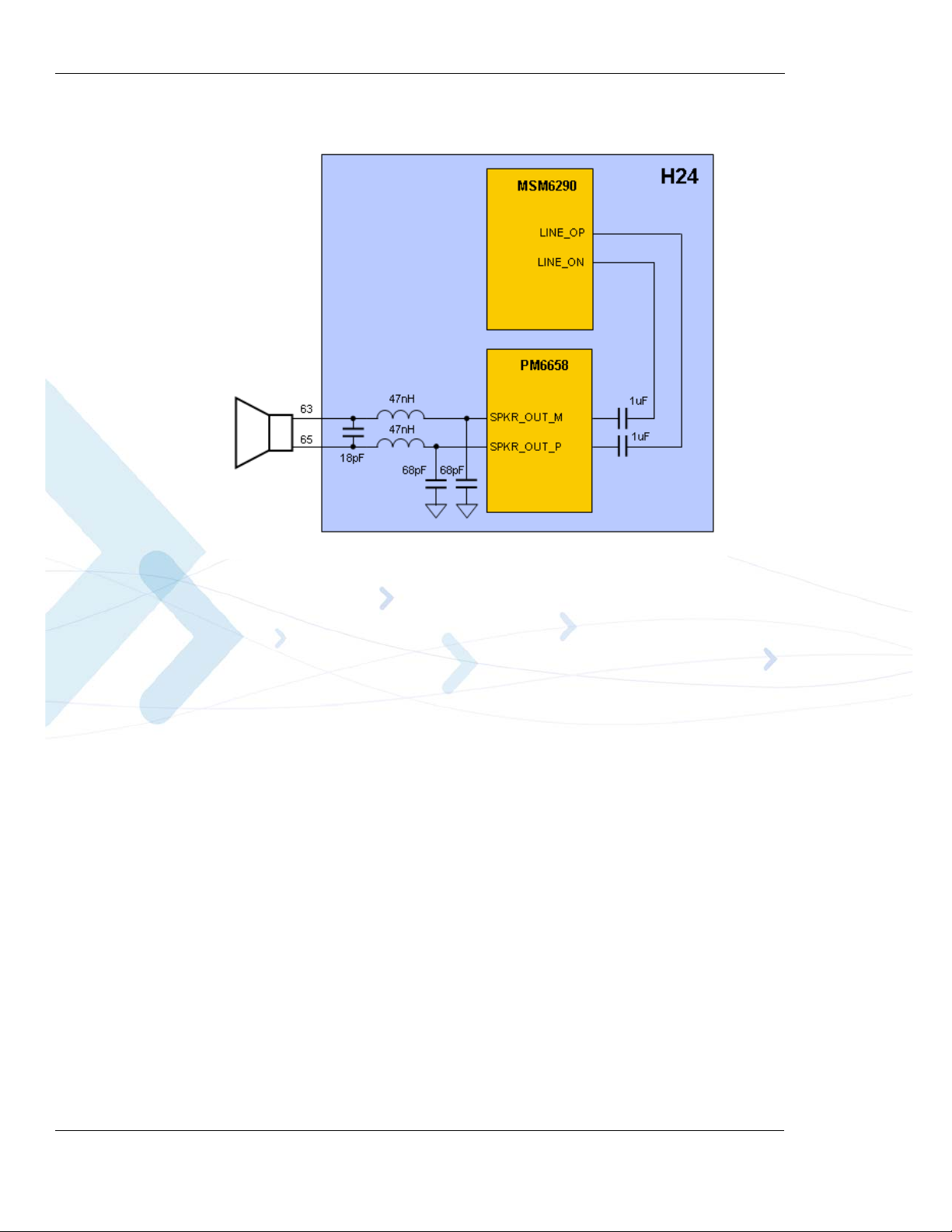
Audio Interface
For gain levels, please refer to H24 AT Commands manual - 6802986C37.
Figure 2-12: External Speaker
Audio Design
The audio quality delivered by H24 is highly affected by the application audio design,
particularly when using the analog audio interface. Therefore, special care must be taken when
designing the H24 audio interface. Improper design and implementation of the audio interface
will result in poor audio quality.
Poor audio quality is a result of electrical interferences, or noises, from circuits surrounding the
audio interface. There are several possible sources for the audio noise:
• Transients and losses on the power supply
• EMI from antenna radiations
• Digital logic switching noise
Most of the audio noise originates from the GSM transmit burst current surges (217 Hz TDMA
buzz), which appear on the main power supply lines and antenna, but also indirectly penetrate the
internal application's supplies and signals. The noises are transferred into the H24's audio circuits
through the microphone input signals and then are amplified by the H24's internal audio
amplifiers.
To minimize the audio noise and improve the audio performance the microphone and speaker
signals must be designed with sufficient protection from surrounding noises.
The following guidelines should be followed to achieve best audio performance:
• Reference the microphone input circuits to the H24 AGND interface signal.
• If using single-ended audio outputs, they should be referenced to the H24 AGND interface
signal.
32 H24 - Module Hardware Description November 15, 2009
Page 57

Chapter 2: Hardware Interface Description
• Keep the audio circuits away from the antenna.
• Use RF filtering capacitors on the audio signals, as described in Table 2-3.
• The audio signals should not be routed adjacent to digital signals.
• Isolate the audio signals by a surrounding ground plane or shields.
• Filter internal supplies and signals that may indirectly affect the audio circuits, from noises
and voltage drops.
Analog Ground
The H24 interface incorporates a dedicated analog ground contact, AGND pin 59, which is
internally connected to the H24's ground. The AGND signal is intended to provide a separate
ground connection for the application's external audio devices and circuits.
This signal provides an isolated ground connection directly from H24, which is separated from
the noisy digital ground of the application. It is recommended to connect this signal to analog
audio devices and circuits used by the application. Using a separate analog ground minimizes
audio noises and improves the audio circuit's immunity from external interferences.
Digital Audio Interface
The H24 digital audio interface is a serial Pulse Code Modulation (PCM) bus, which uses linear
2's compliment coding. H24 is the PCM bus master, supplying the clock and sync signals to the
application.
The H24 digital interface is a 4 signal PCM bus, which includes a bit clock output signal for the
bus timing, a frame sync output signal for audio sampling timing, and serial data input and output
signals.
Important: The PCM bus signals are shared internally by the analog audio interface and the
digital audio interface. Therefore, when using the analog audio interface the PCM
bus signals must be tri-stated or disconnected at the interface connector.
The digital audio interface supports 4 types of audio data formats, which define the PCM bus
configuration and data rates:
• Voice band audio - Intended for speech during voice calls and for mono rings and alerts.
• Stereo audio - Includes 3 audio formats that support high quality stereo ring tones and alerts.
Voiceband Audio
This digital voice audio format is used for speech during voice calls and for mono rings and
alerts.
The PCM bus signal's configuration for voiceband audio is:
• PCM_CLK - 2048 kHz serial clock
• PCM_FS - 8 kHz bit-wide frame-sync
• PCM_DOUT - 13-bit linear audio data output
• PCM_DIN - 13-bit linear audio data input
November 15, 2009 H24 - Module Hardware Description 33
Page 58

Audio Interface
The analog audio is sampled at an 8 kHz rate and converted to linear 13-bit serial PCM audio
data. The serial data is transferred on the PCM bus in 16-bit word format, which includes 13
sampled data bits, and 3 added zero value bits.
The 16-bit serial data is transferred in both directions after each sync signal's falling edge. The
sync signal pulse duration is one clock period, after which the serial data is transferred in both
directions for 16 consecutive clock periods.
Following the 16-bit data transfer, the serial input and output data signals inactivate until the next
sync pulse, which occurs every 125 µS (8 kHz). It is recommended the serial data signals will be
High-Z during the inactive period.
Important: In digital audio mode the input and output gains cannot be controlled by AT
commands.
Figure 2-13 illustrates the PCM bus format of the voiceband audio configuration.
Figure 2-13: Voiceband Mode PCM Bus Coding Format
34 H24 - Module Hardware Description November 15, 2009
Page 59

Controls and Indicators Interface
The H24 incorporates several interface signals for controlling and monitoring the module's
operation. The following paragraphs describes these signals and their operation.
Table 2-6 gives a description of the controls and indicators signals.
Chapter 2: Hardware Interface Description
Table 2-6:
Controls and Indicators
Connector Pin Signal Name Description
25 RESET_N H24 system reset output indicator.
When high, H24 is operating.
27 VREF 2.6V regulated output.
Supplies external circuits up to
300mA.
16 WKUPO_N Host application wake-up signal indi-
cator.
49 Network status
indicator
39 TXEN_N Transmission burst indication.
28, 30, 32, 34, 36,
38, 40, 42
GPIO 1-8 General purpose IO signals for cus-
Network status indicator.
(GPRS/GSM/WCDMA)
tomer use.
Reset
The RESET_N output signal indicates the H24's operating status. This signal is set high after
power up, when H24 is operating. It is set low when H24 is powered off.
When the RESET_N signal is low, the H24 interface signals are disabled and do not represent any
valid data or state. Furthermore, any input signals connected to the H24 interface must be
disabled (tri-state) or set low when RESET_N is low.
VREF Reference Regulator
The H24 incorporates a regulated voltage output, VREF. The regulator provides a 2.6V output for
use by the customer application. This regulator can source up to 300 mA of current to power any
external digital circuits.
Important: The VREF regulator is powered from the H24's main power supply, and therefore
any current sourced through this regulator originates from the H24 VCC supply.
The overall VCC current consumed by H24 is directly affected by the VREF
operation. The H24 current consumption rises with respect to the current sourced
through VREF.
The VREF regulator incorporates 3 operating modes that are controlled by the AT+MVREF
command. These modes define the regulator operating state relative to the H24's operating mode.
November 15, 2009 H24 - Module Hardware Description 35
Page 60
Controls and Indicators Interface
OFF Mode
In this mode the VREF regulator is disabled and its output drops to 0V, regardless of the H24
operating state.
Sleep Mode
The 300 mA rated linear regulator offers a low power mode to reduce its quiescent current during
the module’s sleep mode. This mode uses reduced current in the feedback loop, causing degraded
performance (PSRR, output current capability, etc.). In fact, if the load increases beyond 1 mA
the output voltage can go out of specification. This mode should only be used when the module is
in its sleep mode.
Active Mode
In this mode the VREF regulator is always fully active while H24 is operating, regardless of the
H24 operating mode.
Table 2-7 gives the VREF specifications.
Table 2-7:
VREF Specifications
Parameter Conditions Min Typ Max Unit
V
OUT
I
OUT
Load regulation
Line regulation
PSRR 40 dB
-3% 2.6 +3% V
300 mA
0.65 %
0.2 %/V
Wakeup Out
Some applications incorporate their own power saving mode, in which they operate with minimal
functionality, including disabling of interfaces and serial communications.
The wakeup-out (WKUPO_N) signal is an active low output, which is designed to support a low
power mode feature in the host application. This signal is used by H24 to indicate that it requires
to communicate with the host application through the serial interface, due to an incoming call or
data, or an unsolicited event. Applications that incorporate a low power mode should use this
signal as an indication to switch from low power mode to normal operation, and activate the serial
interface.
The wakeup-out mechanism, using the WKUPO_N signal, is controlled by 2 AT commands (see
Figure 2-14):
• ATS102 - Defines the delay time in milliseconds that H24 will wait, after asserting the
WKUPO_N signal low, before sending data on the serial interface. This delay is required to
allow the application enough time to reactivate from low power mode and switch to normal
36 H24 - Module Hardware Description November 15, 2009
Page 61

Chapter 2: Hardware Interface Description
mode.
If ATS102=0, which is the default value, the WKUPO_N signal and mechanism is disabled.
In case the serial interface incorporates hardware flow control signals, the data will be sent
according to their state, after the ATS102 delay time has expired.
• ATS100 - Defines the application minimal wakeup duration, in seconds, for a single wakeup
event. This time definition is required to avoid frequent unnecessary wakeup events and
consequent ATS102 delays.
The application may return to low power mode after the serial interface has been inactive for
the duration set by ATS100. This duration is measured from the last data sent or received on
the serial interface.
Figure 2-14: WKUPO_N Operation
The following guidelines apply to the wakeup-out mechanism:
• H24 will set the WKUPO_N signal low to indicate that in has data to send through the serial
interface.
• H24 will start sending the data to the application after the delay defined by ATS102.
• The WKUPO_N signal will remain low while data is being sent to the host application.
• The host application should keep its serial interface active, and not switch to low power
mode, while the WKUPO_N signal is low.
• H24 will set the WKUPO_N signal high when it has completed sending the data.
• The application serial interface must stay active, and not switch to low power mode, for the
duration set by ATS100, after WKUPO_N is set high.
• H24 will not set the WKUPO_N signal low if it needs to send additional data during the
ATS100 delay time.
• The application may switch to low power mode after the WKUPO_N signal is set high and
the serial interface has been inactive for the duration set by ATS100.
Network Connection Detection
The network connection output signal (Pin 49) indicates the network (GPRS/EGPRS or
WCDMA/HSPA) connection status. When H24 is connected to a network, this signal is enabled.
When H24 is not connected to the GPRS/EGPRS or WCDMA/HSPA network this signal is
disabled. This pin (Pin 49) is enabled by the command AT+MCWAKE.
November 15, 2009 H24 - Module Hardware Description 37
Page 62

Controls and Indicators Interface
Transmission Indicator
The TXEN_N output signal indicates when H24 is transmitting over the GSM or CDMA
network. This signal follows the H24 GSM transmit bursts. This signal is set low during
transmission burst, and set high when no transmission is in progress.
Figure 2-15 shows the TXEN_N operation.
Figure 2-15: TXEN_N Operation
General Purpose I/O
The H24 incorporates 8 general purpose IO signals for the user application. Each GPIO signal
may be configured and controlled by AT command. These signals may be used to control or set
external application circuits, or to receive indications from the external application.
38 H24 - Module Hardware Description November 15, 2009
Page 63
Antenna Interface
The H24 antenna connector is the RF interface to the GSM/WCDMA network.
Chapter 2: Hardware Interface Description
The antenna interface is terminated by an MMCX connector type, which is 50
Ω impedance
matched at the relevant GSM frequencies.
The antenna or antenna application must be installed properly to achieve best performance.
Table 2-8 gives the antenna interface specifications.
Table 2-8: Antenna Interface Specifications
Parameter Conditions Specifications
TX 824 - 849 MHz
GSM 850
GSM 900
DCS 1800
PCS 1900
Gain For antenna gain please refer to
RX 869 - 894 MHz
TX 880 - 915 MHz
RX 925 - 960 MHz
TX 1710 - 1785 MHz
RX 1805 - 1880 MHz
TX 1850 - 1910 MHz
RX 1930 - 1990 MHz
“Antenna Installation” .
Impedance 50Ω
VSWR Less than: 2.5:1
WCDMA B1
2100
WCDMA B2
1900
WCDMA B5
850
WCDMA B4
1700
TX 1920-1980 MHz
RX 2110 - 2170 MHz
TX 1850-1910 MHz
RX 1930-1990 MHz
TX 824 - 849 MHz
RX 869 - 894 MHz
TX 1710 - 1755 MHz
RX 2110 - 2155 MHz
It is the Integrator's responsibility to design the antenna or antenna assembly used with the H24.
This will highly affect the RF performance of the H24 (dropped calls, battery consumption etc.).
The following guidelines should be followed:
• Make sure that the antenna or antenna assembly matches the Antenna Interface
Specifications.
• Use low loss RF cable and connectors keeping cable runs to a minimum.
November 15, 2009 H24 - Module Hardware Description 39
Page 64

Antenna Interface
40 H24 - Module Hardware Description November 15, 2009
Page 65

Chapter 3: Electrical and Environmental Specifications
Absolute Maximum Ratings
Table 3-1 gives the maximum electrical characteristics of the H24 interface signals.
Caution: Exceeding the values may result in permanent damage to the module.
Table 3-1: Maximum Ratings
Parameter Conditions Min Max Unit
VCC Supply -0.2 4.2 V
Digital Input Signals
(Except for IGN,
VBUS, USB_DP,
USB_DN)
Analog Input Signals
(Audio, A/D interfaces)
All Input Signals
(Except for IGN,
VBUS, USB_DP,
USB_DN)
IGN signal -0.2 16 V
VBUS signal -0.2 5.25 V
USB_DP, USB_DN -0.2 3.6 V
H24 powered on -0.2 2.9 V
H24 powered on -0.2 2.9 V
H24 powered off -0.2 0.2 V
Caution: It is not recommended to connect the ignition pin directly to the car’s ignition wire
without adequate protection.
November 15, 2009 H24 - Module Hardware Description 41
Page 66

Environmental Specifications
Environmental Specifications
Table 3-2 gives the environmental operating conditions of the H24 module.
Caution: Exceeding the values may result in permanent damage to the module.
Table 3-2: Environmental Ratings
Parameter Conditions Min Max Unit
Ambient Operating
Temperature
Storage Temperature -40 85 °C
ESD At antenna connector
Restricted operation
(For more details
please contact
M2M.CustomerCare@motorola.com)
Contact
Air
At interface connector
Application Interface Specifications
Table 3-3 summarizes the DC electrical specifications of the application interface connector
signals.
Important: Interface signals that are not used by the customer application must be left
unconnected. H24 incorporates the necessary internal circuitry to keep unconnected
signal in their default state. Do not connect any components to, or apply any voltage
on, signals that are not used by the application.
-30 65 °C
-30 85 °C
KV
± 8
± 15
± 1
Important: Signals that are defined as "Do Not Use", or DNU, must remain externally
unconnected in any case. These signals are reserved for future use.
42 H24 - Module Hardware Description November 15, 2009
Page 67

Chapter 3: Electrical and Environmental Specifications
The following table gives a brief description of the 70 pins connector for quick integration.
GND 1 2 GND
GND 3 4 GND
VCC 5 6 VCC
VCC 7 8 VCC
RTS_N 9 10 USB_VBUS
RXD_N 11 12 USB_DP
DSR_N 13 14 USB_DN
CTS_N 15 16 WKUPI_N
DCD_N 17 18 PCM_DIN
DTR_N 19 20 PCM_DOUT
TXD_N 21 22 PCM_CLK
RI_N 23 24 PCM_FS
RESET_N 25 26 WKUPO_N
VREF 27 28 GPIO1
RXD2 29 30 GPIO2
TXD2 31 32 GPIO3
RTS2 33 34 GPIO4
CTS2 35 36 GPIO5
ADC1 37 38 GPIO6
TXEN_N 39 40 GPIO7
ANT_DET (NC) 41 42 GPIO8
ADC243 44SIM_RST_N
USB_ID 45 46 SIM_CLK
ADC347 48SIM_VCC
GPRS 49 50 SIM_PD_N
IGN 51 52 SIM_DIO
ON_N 53 54 HEADSET_P
HDST_INT_N 55 56 Chip SIM reset
MIC2_P 57 58 GPS_PWR
AGND 59 60 NC
MIC1_P 61 62 MIC1_N
ALRT_N 63 64 NC
ALRT_P 65 66 NC
SPKR_N 67 68 Coin Cell
SPKR_P 69 70 MIC2_N
November 15, 2009 H24 - Module Hardware Description 43
Page 68
Application Interface Specifications
Table 3-3: Interface Specifications
Level
Pin #
Signal
Name
Description I/O
Active
H/L
Internal
PU/PD
Parameter Conditions
Min Typ Max Units
Power:
1
2
GND Ground
3
4
5
6 1.7 1.8 A
7 40 50 uA
VCC DC power
supply
I
V
IN
I
MAX
I
OFF
VCC = 3.6 V
3.3 3.6 4.2 V
8
68 COIN
I H 1.8 3 3.25 V
CELL
58 GPS ANT
POWER
27 VREF Reference
Do not
connect
I V
O1.82.63
regulator output
300VmA
Control:
16 WKUPI_N H24 wakeup
IL PU V
input
26 WKUPO_
N
25 RESET_N Reset signal
Host wakeup
output
OL V
OL V
output
53 ON_N On/Off switch I L PU V
51 IGN Ignition input I H PD V
39 TXEN_N Transmit indi-
OH V
cator
49 GPRS GPRS/
OH I
EGPRS coverage indicator
Primary UART:
I
IH
V
IL
OH
V
OL
OH
V
OL
IH
V
IL
IL
V
IH
OH
V
OL
< 2mA 2.0 2.602.9
OUT
I
< 2mA 2.15 2.6
OUT
I
< 2mA 2.15 2.6
OUT
2.0 2.602.9
0
3.3
I
< 2mA 2.15 2.6
OUT
< 2mA 2.15 2.6
OUT
00.45
00.45
00.45
V
0.4
V
V
V
0.4
0.416V
V
V
00.45
44 H24 - Module Hardware Description November 15, 2009
Page 69
Chapter 3: Electrical and Environmental Specifications
Table 3-3: Interface Specifications (Cont.)
Pin #
Signal
Name
Description I/O
Active
H/L
Internal
PU/PD
Parameter Conditions
21 TXD_N UART1 TXD I L PD V
11 RXD_N UART1 RXD O L V
9 RTS _N UART1 RT S I L V
15 CTS_N UART1 CTS O L V
19 DTR_N UART1 DTR I L PU V
13 DSR_N UART1 DSR O L V
17 DCD_N UART1 DCD O L V
23 RI_N UART1 RI O L V
Level
Min Typ Max Units
IH
V
IL
OH
V
OL
IH
V
IL
OH
V
OL
IH
V
IL
OH
V
OL
OH
V
OL
OH
V
OL
I
OUT
< 2mA
2.0 2.602.9
0.4
2.15 2.6
00.45
2.0 2.602.9
0.4
2.15 2.6
00.45
V
2.0 2.602.9
0.4
2.15 2.6
00.45
2.15 2.6
00.45
2.15 2.6
00.45
Secondary UART:
29 RXD2_N Do not
connect
31 TXD2_N Do not
connect
33 RTS2_N Do not
connect
35 CTS2_N Do not
connect
USB I/F:
10
USB_VBUS
USB bus
power
12 USB_DP USB bus
serial data
14 USB_DN USB bus
serial data
45 USB_ID Do not
connect
OL
IL PD
IL PD
OL
I 4.75 5 5.25 V
I/O H 3.6 V
I/O L
IL
SIM I/F:
November 15, 2009 H24 - Module Hardware Description 45
Page 70
Application Interface Specifications
Table 3-3: Interface Specifications (Cont.)
Level
0.4
Pin #
50
Signal
Name
SIM_PD_N
Description I/O
SIM presence
detect
IL PU V
Active
H/L
Internal
PU/PD
Parameter Conditions
IH
V
IL
Min Typ Max Units
2.0 2.602.9
48 SIM_VCC SIM supply O L 1.5 3 3.05 V
44
SIM_RST_
N
52 SIM_DIO SIM serial
46 SIM_CLK SIM clock O H 2.7
56 Chip SIM
reset
SIM reset O L V
I/O H 2.7
data
Chip SIM
IL
reset
2.7
IH
V
IL
I
OUT
< 2mA
1.65
2.85
1.8
3
1.95
2.85
1.65
1.831.95
2.85
1.65
1.831.95
(In case Chip
SIM incorporated,
short-circuit
this pin to pin
44).
Digital Audio:
V
V
18 PCM_
DIN
20
22
PCM_
DOUT
PCM_CLK
Digital audio
receive
Digital audio
transmit
Digital audio
clock
24 PCM_FS Digital audio
frame sync.
IH PD V
OH V
OH V
OH V
IH
V
IL
OH
V
OL
OH
V
OL
OH
V
OL
I
OUT
< 2mA
2.0 2.602.9
0.4
2.15 2.6
00.45
V
2.15 2.6
00.45
2.15 2.6
0 045
46 H24 - Module Hardware Description November 15, 2009
Page 71
Chapter 3: Electrical and Environmental Specifications
Table 3-3: Interface Specifications (Cont.)
Pin #
Signal
Name
Description I/O
General Purpose I/O:
28 GPIO1 General pur-
pose I/O
30 GPIO2 General pur-
pose I/O
32 GPIO3 General pur-
pose I/O
34 GPIO4 General pur-
pose I/O
36 GPIO5 General pur-
pose I/O
38 GPIO6 General pur-
pose I/O
40 GPIO7 General pur-
pose I/O
42 GPIO8 General pur-
pose I/O
Active
H/L
Internal
PU/PD
Parameter Conditions
I/O PU V
I/O PU
I/O PU
I/O PU
I/O PU V
I/O PU
I/O PU
I/O PU
Level
Min Typ Max Units
IH
V
IL
I
< 2mA
OH
V
OL
OUT
2.0 2.602.9
0.4
V
2.15 2.6
00.45
Analog Audio:
67 SPKR_N Earpiece
negative
69 SPKR_P Earpiece
positive
63 ALRT_N Alert speaker
negative
65 ALRT_P Alert speaker
positive
61 MIC1_P Microphone
input positive
62 MIC1_N Microphone
input negative
59 AGND Audio ground
57 MIC2_P Headset
microphone
input positive
70 MIC2_N Headset
microphone
input negative
OR
O1.8V
OR
O5.0V
IR
I21050mV
IR
I21050mV
L
Differential
AV p p
L
Differential
AV p p
IN
Differential
AV p p
IN
Differential
AV p p
32 Ω
8 Ω
1kΩ
1kΩ
November 15, 2009 H24 - Module Hardware Description 47
Page 72
Application Interface Specifications
Table 3-3: Interface Specifications (Cont.)
Pin #
54 HDST_
55 HDST_
A/D (ADC):
37 ADC1 General pur-
43 ADC2 General pur-
47 ADC3 General pur-
Not Connected:
41 ANT_DET Do not
60 NC Do not
Signal
Name
SPKR
INT_N
Description I/O
Headset
Speaker output
Headset
detect
interrupt
pose A/D
pose A/D
pose A/D
connect
connect
Active
OR
I 47k PU V
IVIN02.9V
I
I
H/L
Internal
PU/PD
Parameter Conditions
Min Typ Max Units
L
AV p p
IH
V
IL
active 0 2.6 V
V
IN
Single Ended 32
I
< 2mA 2.0 2.602.9
OUT
Level
1.8ΩV
V
0.4
64 I2C_SCL Do not
connect
66 I2C_SDA Do not
connect
Note: R(PD) =210kΩ, R(PU) =390kΩ
48 H24 - Module Hardware Description November 15, 2009
Page 73

Chapter 4: Mechanical Specifications
1
2.1
2.3
45.2
24.4
3
6.1
5.4
2
6.6 23.9
10
19.8
18.2
2.2
10.5
32.6
0.3
13.9
2.4
Application PCB
H24
3.0mm Stacking
H24 General Dimensions
UFL Diversity RF Connector
Pin #1
Pin #69
70 Pin
Interface
Connector
MMCX Main RF Connector
UFL GPS RF Connector
Board Dimensions
Figure 4-1 describes the H24 mechanical characteristics.
Figure 4-1: H24 Mechanical Characteristics
November 15, 2009 H24 - Module Hardware Description 49
Page 74

Interface Connector Specifications
Interface Connector Specifications
The H24 uses a single 70-pin, 0.5 mm pitch, board to board connector for the application
interface, as described in Tab le 4 -1.
Table 4-1: H24 interface connector options
H24 Connector Mating Connector Stacking Height
Molex 53748-0708 Molex 52991-0708 3.0 mm
Figure 4-2 shows the H24 interface connector.
Figure 4-2: H24 Interface Connector
Table 4-2 describes the H24 interface connector characteristics.
Table 4-2: Interface Connector Specifications
Parameter 53748 (3.0 mm)
Contacts 70
Rows 2
Pitch 0.5 mm
Maximum Current 500 mA
Maximum Voltage 50 V
Contact Resistance 50 mΩ maximum
Insulation
Resistance
Durability 50 mated cycles
Stacking Height 3.0 mm
100 MΩ minimum
maximum
Mates with Molex 52991-0708
50 H24 - Module Hardware Description November 15, 2009
Page 75

Chapter 4: Mechanical Specifications
Mating Connector
The mating connector incorporates the same electrical and mechanical characteristics as the
corresponding H24 interface connector, and is described in Table 4-2.
Figure 4-3 provides a reference drawing of the mating connector mechanical dimensions.
Figure 4-3: Mating Connector Dimensions
For more information on the H24 mating connector, please refer to the Molex web site at
http://www.molex.com/molex/index.jsp.
November 15, 2009 H24 - Module Hardware Description 51
Page 76
MMCX Connector Specifications
MMCX Connector Specifications
The H24 uses a standard MMCX receptacle connector for the radio interface.
Figure 4-4 shows the MMCX connector dimensions.
Figure 4-4: MMCX Connector Dimensions
Table 4-3 describes H24 RF connector characteristics.
Table 4-3: RF Connector Specifications
Parameter Specifications
Rated Voltage 335 V
Impedance 50 Ω
Contact Resistance 5 mΩ center contact
Insulation
Resistance
Insertion Force 3.4 lbs maximum
Withdrawal Force 4.5 lbs maximum
Contact Retention
Force
Durability 500 mated cycles maximum
RMS
2.5 mΩ outer contact
1000 MΩ
4 lbs maximum
Mating Connector
The RF mating connector should be a standard MMCX plug connector or cable assembly, which
corresponds to the H24 MMCX connector specifications.
Any standard MMCX connector or application from different manufacturers may be mated with
H24.
52 H24 - Module Hardware Description November 15, 2009
Page 77

Chapter 4: Mechanical Specifications
Such a cable assembly example is the Huber-Suhner PN 11_MMCX-50-1-2/111_OH, which is
illustrated in Figure 4-5.
Figure 4-5: Optional MMCX Cable Assembly
November 15, 2009 H24 - Module Hardware Description 53
Page 78

U.FL Connector Specifications
U.FL Connector Specifications
The H24 uses a standard U.FL receptacle connector for the radio interface.
Figure 4-6 shows the U.FL connector dimensions.
Figure 4-6: U.FL Connector Dimensions
Table 4-4 describes the U.FL connector characteristics.
Table 4-4: U.FL Connector Specifications
Parameter Specifications
Characteristic
Impedance
Frequency Range DC to 6 GHz
VSWR (mated pair) 1.30 max DC to 3 GHz
Insertion Loss
(connectors only)
54 H24 - Module Hardware Description November 15, 2009
50 Ohms
1.40 max 3 to 6 GHz (cable dependent)
0.24 dB max DC to 6 GHz
Page 79

Chapter 4: Mechanical Specifications
Table 4-4: U.FL Connector Specifications (Cont.)
Parameter Specifications
Rated voltage 60 VAC (rms) - standard recept (Styles
A, B)
Dielectric
Withstanding
Voltage
Insulation
Resistance
Contact Resistance
(connectors only)
Durability 30 cycles - standard recept (Styles A, B)
Disengagement
Force
Center Contact
Retention force
Tape/Reel
Packaging
(receptacle)
Operating
T emperature
Mating Connector
200 VAC, 50 Hz for 1 min (at sea level)
500 Megohms min
20 milliohms max (Center)
10 milliohms max (Outer, Plug)
10 milliohms max (Outer, Receptacle)
2N min perpendicular
4N min orthogonal
0.15N min
12mm carrier per EIA-481
40°C to + 90°C
The RF mating connector should be a standard U.FL plug connector or cable assembly, which
corresponds to the H24 U.FL connector specifications.
Only Hirose U.FL mating cable may be mated with H24. A family of Hirose maning cables are
available.
Such a cable assembly example is the Hirose U.FL-LP-040 is U.FL-R-SMT, which is illustrated
in Figure 4-7.
Figure 4-7: U.FL Mating Connector
For more details regarding Hirose mating cable assemblies, refer to
http://www.hirose.co.jp/cataloge_hp/e32119372.pdf.
November 15, 2009 H24 - Module Hardware Description 55
Page 80

H24 Mounting
H24 Mounting
The H24 incorporates 2 mechanical holes for installing the module onto the application board.
The holes are 2.4 millimeters in diameter, which accommodates several types of mechanical
elements.
Several mechanical approaches may be applied to mount and fasten H24 to the application board.
Using M2 screws with suitable washers to mount the module onto spacers, a bracket or chassis is
a recommended design.
Special attention must be paid to the area surrounding the H24 mounting holes. A grounding pad
of 4.4 millimeters in diameter surrounds these holes. The diameter and area of this pad must not
be exceeded by any mechanical or electrical element. Several electrical components, which are
not shielded, are located near the holes. These components must not be in contact with the
mounting elements or with other parts of the application board, and care must be taken to avoid
any damage.
Figure 4-8 depicts the H24 mounting area.
Figure 4-8: H24 Mounting Area
The holes are used for mechanical mounting of H24 to the application board but also for
grounding support. Using conductive elements to install H24, significantly improves the overall
grounding of the module and therefore improves the H24 performance and stability.
It is required to use screws or other mechanical elements to fasten H24 to the application board,
but it is highly recommended to use conductive elements to improve the module's performance.
The preferred mounting screw head types are:
• "Allen" head with a champer - the best choice.
• "Star" head - good.
• "Philips" head - may cause damage to nearby components.
56 H24 - Module Hardware Description November 15, 2009
Page 81

Chapter 5: Service and Testing
Service
This section provides contact information for any possible queries that may arise, for example:
• Have questions?
• Having trouble getting the Developer Board set up?
• Technical questions?
• Configuration questions/problems?
• Technical operating problems?
• Need documentation?
Who to Contact?
Use this following email address to contact customer assistance:
M2M.CustomerCare@motorola.com
Required Query Information
Every new call/problem report, directly from a Direct Customer or from a distributor, should be
directed to the help desk email address noted above in “Who to Contact?” . It is recommended to
report each individual issue in a separate email. The following information is required when
reporting a problem:
• Customer name and address
• Customer contact information for this request, including:
– Name
– Telephone
– Fax number
– Mobile number
– Email address
• Product name (H24)
• Software version of the unit (ATI8i9 command) or model number
• PCB version (located on the PCB near the RF connector).
• In addition to the information requested above, send the following AT commands and the
HyperTerminal log with the responses:
• AT+CMEE=2 // to get textual error message
• AT+CPIN? // to get SIM card status
November 15, 2009 H24 - Module Hardware Description 57
Page 82

Service
• AT+CREG? // to see if the TXVR is registered to the network
• AT+CSQ // to get the signal strength (RX level)
• AT+CGSN // to read the IMEI number of the unit
• AT\S // to get the setting of basic AT commands
• AT+CMER=0,0,1,1 // to get messages and indicators from the handset display to the DTE
58 H24 - Module Hardware Description November 15, 2009
Page 83
Acronyms and Abbreviations
A
BCD
E
Abbreviation Full Name
A AMR
A AOC
B BR
B bps
C CSD
C CTS
D DCD
D DCE
D DCS
D DOC
D DRX
D DSP
D DSR
D DTE
D DTMF
D DTR
D DTX
Adaptive Multi Rate
Advice of Charge
Baud Rate
Bits Per Second
Circuit Switched Data
Clear to Send
Data Carrier Detect
Data Communication Equipment (such as modems)
Digital Cellular System (GSM in the 1800MHz band)
Department of Communications (Canada)
Discontinuos Reception
Digital Signal Processor
Data Set Ready
Data Terminal Equipment (such as terminals, PCs and so on)
Dual Tone MultiFrequency
Data Terminal Ready
Discontinuos Transmission
E EFR
E EGPRS
E EGSM
E EIRP
November 15, 2009 H24 - Module Hardware Description Acr & Abbr-1
Enhanced Full Rate
Enhanced General Packet Radio Service
Extended Global System for Mobile Communications
Effective Isotropic Radiated Power
Page 84

Abbreviation Full Name
F
G
HILMO
P
E EMC
E EOTD
E EPOS
E ERP
E ESD
E ETSI
F FCC
F FR
F FTA
G GCF
G GPIO
G GPRS
G GSM
H HR
H HSDPA
Electromagnetic Compatibility
Enhanced Observed Time Difference
Electronic Point of Sale
Effective Radiated Power
Electrostatic Discharge
European Telecommunication Standards Institute
Federal Communications Commission (U.S.)
Full Rate
Full Type Approval
GSM Certification Forum
General Purpose Input/Output
General Packet Radio Service
Global System for Mobile Communications
Half Rate
High-Speed Downlink Packet Access
I IC
L LNA
M MMCX
M MO
M MT
O OEM
P PCB
P PCL
P PCM
P PCS
P PD
Integrated Circuit
Low-noise Amplifier
Miniature Micro Coax
Mobile Originated
Mobile Terminated
Original Equipment Manufacturer
Printed Circuit Board
Power Class Level
Pulse Code Modulation
Personal Communication System (also known as GSM 1900)
Pull Down
Acr & Abbr-2 H24 - Module Hardware Description November 15, 2009
Page 85

Abbreviation Full Name
RST
Acronyms and Abbreviations
P PDA
P PDU
P PLL
P PTCRB
P PU
R R&TTE
R RMS
R RI
R RTS
S SAR
S SIM
S SMS
S SPI
T TDMA
T TIS
T TRP
Personal Data Assistant
Packet Data Unit
Phase-locked Loop
PCS-1900 Type Certification Review Board (GSM North America)
Pull Up
Radio and Telecommunications Terminal Equipment
Root Mean Square
Ring Indicator
Request To Send
Specific Absorption Rate
Subscriber Identity Module
Short Message Service
Serial Peripheral Interface
Time Division Multiple Access
Transmitter Isotropic Sensitivity
Transmitter Radiated Power
November 15, 2009 H24 - Module Hardware Description Acr & Abbr-3
Page 86

Abbreviation Full Name
U
V
W
U UART
U USB
U USSD
V VCC
V VSWR
V WCDMA
Universal Asynchronous Receiver Transmitter
Universal Serial Bus
Unstructured Supplementary Services Data
Voltage Common Collector
Voltage Standing Wave Ratio
Wideband Code Division Multiple Access
Acr & Abbr-4 H24 - Module Hardware Description November 15, 2009
Page 87

Index
A
Antenna Installation, x
Approvals
Regulatory, 6
B
Block Diagram Description, 9
E
Environmental
Specifications
, 3
H
H24
Abbreviations, 2
Antenna Installation, x
Block Diagram Description, 9
Product Specifications, 2
Regulatory Approvals, 6
Safety Precautions, ix
Standards, x
Terms and Abbreviations, 2
User Operation, ix
O
Organization of Manual, xix
P
Physical Specifications, 2
Precautions, ix
Product Specifications, 3
R
Regulatory Approvals, 6
S
Safety Precautions, ix
Specifications, 2
Environmental, 3
Physical, 2
Standards, x
T
Terms, 2
U
User Operation, ix
November 15, 2009 H24 - Module Hardware Description Index-1
Page 88

Index U - U
Index-2 H24 - Module Hardware Description November 15, 2009
Page 89

Page 90

@6802986C38@
6802986C38-D
MOTOROLA and the Stylized M Logo are registered in the US Patent & Trademark Office.
All other product or service names are the property of their respective owners.
© Copyright 2007 Motorola, Inc.
Java™ Technology and/or J2ME™ : Java and all other Java–based marks are trademarks or registered trademarks of Sun Microsystems, Inc. in the U.S. and other countries.
UNIX® : UNIX is a registered trademark of The Open Group in the United States and other countries.
 Loading...