

Page 1

©
2003
g20 Developer’s Kit
DRAFT 1 (31.3.03)
Motorola Communications Ltd.,
A subsidiary of Motorola Inc.
All rights reserved.
Developer’s Guide
98-08901C67-O
Page 2

REVISION HISTORY
DRAFT 1 (31.3.03)
Revision Date Purpose
Page 3

g20
DRAFT 1 (31.3.03)
Developer’s Kit
CONTENTS
REVISION HISTORY ................................................................................................................................................................ii
PREFACE
1.1 SCOPE OF THIS MANUAL .................................................................................................................................................1
1.2 WHO SHOULD USE THIS MANUAL .................................................................................................................................1
1.3 DISCLAIMER ........................................................................................................................................................................1
1.4 REGULATORY REQUIREMENTS .....................................................................................................................................1
1.5 REGULATORY STATEMENT.............................................................................................................................................1
1.6 SAFETY .................................................................................................................................................................................2
1.6.1 User Operation ............................................................................................................................................................2
1.6.2 Antenna Installation ....................................................................................................................................................2
1.7 APPLICABLE DOCUMENTS ..............................................................................................................................................2
1.8 HOW THIS MANUAL IS ORGANIZED..............................................................................................................................2
INTRODUCTION
2.1 GENERAL DESCRIPTION...................................................................................................................................................3
2.2 TERMS AND ABBREVIATIONS ........................................................................................................................................3
2.3 SAFETY PRECAUTIONS.....................................................................................................................................................3
DEVELOPER BOARD AND INTERFACES DESCRIPTION
3.1 GENERAL..............................................................................................................................................................................5
3.1.1 Developer Board Features...........................................................................................................................................6
3.1.2 Developer Board Connectivity....................................................................................................................................7
3.1.3 Quick Start...................................................................................................................................................................8
3.2 COMMUNICATIONS INTERFACES ................................................................................................................................10
3.2.1 RS232........................................................................................................................................................................10
3.2.2 USB ...........................................................................................................................................................................11
3.2.3 SPI .............................................................................................................................................................................11
3.3 CONNECTORS DESCRIPTION.........................................................................................................................................12
3.3.1 UUT Interface Connector..........................................................................................................................................13
3.4 POWER CONNECTIONS ...................................................................................................................................................15
3.4.1 DC Power Source Operation.....................................................................................................................................15
March 2003
© Motorola Inc., 2003 98-08901C67-O
Page 4

3.4.2 AC Adapter Operation.............................................................................................................................................. 16
DRAFT 1 (31.3.03)
3.4.3 Battery Operation ..................................................................................................................................................... 16
3.4.4 Power Source Selection............................................................................................................................................ 16
3.5 SWITCHES AND JUMPERS.............................................................................................................................................. 17
3.6 LED INDICATORS............................................................................................................................................................. 18
3.7 MMI ..................................................................................................................................................................................... 19
3.7.1 Display...................................................................................................................................................................... 19
3.7.2 Keypad...................................................................................................................................................................... 20
3.8 AUDIO INTERFACE .......................................................................................................................................................... 21
3.8.1 Speaker ..................................................................................................................................................................... 21
3.8.2 Microphone............................................................................................................................................................... 21
3.8.3 Audio Source Selection ............................................................................................................................................ 21
3.8.4 Headset ..................................................................................................................................................................... 22
3.8.5 Alert Speaker ............................................................................................................................................................ 23
3.9 DEVELOPER BOARD PERIPHERALS ............................................................................................................................ 23
3.9.1 SIM Card .................................................................................................................................................................. 23
3.9.2 Entertainment Mute .................................................................................................................................................. 24
3.9.3 LEDs Logic and Control........................................................................................................................................... 24
3.9.4 ADC Test Logic........................................................................................................................................................ 24
3.9.5 Ignition...................................................................................................................................................................... 25
3.9.6 Wakeup..................................................................................................................................................................... 25
3.9.7 AC Adapter Detection Circuit .................................................................................................................................. 25
3.10 ANTENNA CONFIGURATION....................................................................................................................................... 25
3.11 TEST POINTS ................................................................................................................................................................... 26
3.12 ELECTRICAL SPECIFICATIONS................................................................................................................................... 26
MECHANICAL DESCRIPTION
4.1 MECHANICAL REQUIREMENTS FOR MOUNTING THE G20 MODULE ................................................................. 27
SERVICE SUPPORT
5.1 WEB PAGES ....................................................................................................................................................................... 29
5.2 CUSTOMER ASSISTANCE............................................................................................................................................... 29
SCHEMATICS, PLACEMENT AND PARTS LIST
6.1 SCHEMATICS..................................................................................................................................................................... 31
6.2 DEVELOPERS BOARD PLACEMENT ............................................................................................................................ 41
6.3 DEVELOPER BOARD PARTS LIST................................................................................................................................. 43
ERRATA
7.1 SWITCH ASSIGNMENTS CORRECTION....................................................................................................................... 49
INDEX
iv 98-08901C67-O
Page 5

LIST OF FIGURES
DRAFT 1 (31.3.03)
Figure 1. Developer Board with Accessories ...............................................................................................................................5
Figure 2. Developer Board Components ......................................................................................................................................7
Figure 3. Mounting the g20 Module.............................................................................................................................................8
Figure 4. Attaching the RF Cable .................................................................................................................................................8
Figure 5. ADC Test Logic ..........................................................................................................................................................25
Figure 6. Mechanical Mounting Requirements ..........................................................................................................................27
Figure 7. .....................................................................................................................................................................................32
Figure 8. .....................................................................................................................................................................................33
Figure 9. .....................................................................................................................................................................................34
Figure 10. ...................................................................................................................................................................................35
Figure 11. ...................................................................................................................................................................................36
Figure 12. ...................................................................................................................................................................................37
Figure 13. ...................................................................................................................................................................................38
Figure 14. ...................................................................................................................................................................................39
Figure 15. ...................................................................................................................................................................................40
Figure 16. Developer Board Top Layout....................................................................................................................................41
Figure 17. Developer Board Bottom Layout ..............................................................................................................................42
Figure 18. S100 Options Switch Functions ................................................................................................................................49
98-08901C67-O v
Page 6

LIST OF TABLES
DRAFT 1 (31.3.03)
Table 1. Terms and Abbreviations............................................................................................................................................... 3
Table 2. RS232-1 Connector Pinout (J350) ............................................................................................................................... 10
Table 3. USB Connector Pinout (J3).......................................................................................................................................... 11
Table 4. USB Selection (P300 Jumper) ..................................................................................................................................... 11
Table 5. RS232-2 Connector Pinout (J500) ............................................................................................................................... 12
Table 6. Connectors.................................................................................................................................................................... 12
Table 7. g20 Connectors Pinout................................................................................................................................................. 13
Table 8. J230 Connector Pinout................................................................................................................................................. 16
Table 9. P600 Connector Pinout ................................................................................................................................................ 16
Table 10. Power Source (P202 Jumper)..................................................................................................................................... 16
Table 11. Switches and Jumpers ................................................................................................................................................ 17
Table 12. LED Indicators........................................................................................................................................................... 18
Table 13. Display Connector Pinouts (DS800).......................................................................................................................... 19
Table 14. Keypad Functions...................................................................................................................................................... 20
Table 15. Speaker Connector Pinout (J430)............................................................................................................................... 21
Table 16. Microphone Connector Pinout (J460) ........................................................................................................................ 21
Table 17. Audio Source (P420 Jumper) ..................................................................................................................................... 22
Table 18. Headset Connector Pinout (J440)............................................................................................................................... 22
Table 19. Alert Transducer Pinout (LS400)............................................................................................................................... 23
Table 20. SIM Connector Pinouts (J100)................................................................................................................................... 23
Table 21. SIM Detection Logic (P110 Jumper)......................................................................................................................... 24
Table 22. Test Points.................................................................................................................................................................. 26
Table 23. Electrical Specifications............................................................................................................................................. 26
Table 24. Developer Board Parts List........................................................................................................................................ 43
vi 98-08901C67-O
Page 7

1. PREFACE
DRAFT 1 (31.3.03)
1.1 SCOPE OF THIS MANUAL
This manual introduces the g20 Developer's Kit, and describes the technical details required by the data terminal equipment
(DTE) team to successfully integrate the Motorola g20 cellular engine into an original equipment manufacturer (OEM) wireless
host device. With the help of this manual, the DTE team can use the Developer's Kit to conduct a full series of test and evaluation
procedures on the g20, as well as perform application development.
We at Motorola want to make this guide as helpful as possible. Keep us informed of your comments and suggestions for
improvements.
You can reach us by email: GSM support-BSH015@email.mot.com.
1.2 WHO SHOULD USE THIS MANUAL
This manual is intended for all members of the DTE OEM integration team who will use the g20 Developer’s Kit, including
representatives from hardware, software and RF engineering disciplines.
1.3 DISCLAIMER
This guide provides advice and guidelines to OEM teams. Responsibility regarding how the information is used lies entirely
with the OEM. Statements indicating support provided by, or offered by, Motorola are subject to change at any time.
Motorola reserves the right to make any changes to this manual.
1.4 REGULATORY REQUIREMENTS
The Federal Communications Commission (FCC) requires application for certification of digital devices in accordance with
CFR Title 47, Part 2 and Part 15. This includes Electromagnetic Energy Exposure (EME) testing. As the g20 modem is not a
standalone transceiver but is an integrated module, the g20 cannot be tested by itself for EME certification. It is, however, the
integrator’s responsibility to have the completed device tested for EME certification.
1.5 REGULATORY STATEMENT
The following safety precautions must be observed during all phases of the operation, usage, service or repair of any cellular
terminal or mobile incorporating the g20 module. Manufacturers of the cellular terminal are advised to convey the following
safety information to users and operating personnel, and to incorporate these guidelines into all manuals supplied with the product. Failure to comply with these precautions violates safety standards of design, manufacture and intended use of the product.
Motorola assumes no liability for customer failure to comply with these precautions.
1. The g20 must be operated at the voltages described in the technical documentation.
2. The g20 must not be mechanically nor electrically changed. Use of connectors should follow the guidance of the technical
documentation.
3. The g20 is designed the meet the EMC requirements of ETS 300 342.
98-08901C64-O 1
Page 8

Preface
DRAFT 1 (31.3.03)
4. When integrating the g20 into a system, Motorola recommends testing the system to ETS300342-1.
5. The g20 meets the safety requirements of EN60950.
6. Systems using the g20 are subject to mandatory EMC testing under directive 89/336/EEC (see item 3 above). Other
directives, such as the LVD directive 73/23/EE, may also apply to a system using the g20 module.
1.6 SAFETY
1.6.1 User Operation
Do not operate your telephone when a person is within eight inches (20 centimeters) of the antenna. A person or object within
eight inches (20 centimeters) of the antenna could impair call quality and may cause the phone to operate at a higher power level
than necessary, as well as expose that person to RF energy in excess of that established by the FCC RF Exposure Guidelines.
IMPORTANT: The telephone must be installed in a manner that provides a minimum separation distance of 20 cm or more
between the antenna and persons in order to satisfy FCC RF exposure requirements for mobile transmitting devices.
IMPORTANT: To comply with the FCC RF exposure limits and satisfy the categorical exclusion requirements for mobile
transmitters, the requirements described in the section that follows must be met.
1.6.2 Antenna Installation
• A minimum separation distance of 20 cm must be maintained between the antenna and all persons.
• The effective radiated power of the transmitter must be less than 1.5 Watts ERP (2.45 Watts or 33.9 dBm EIRP). This requires
that the combination of antenna gain and feed line loss does not exceed 11 dBi.
1.7 APPLICABLE DOCUMENTS
g20 Cellular Engine Module Description: 9808901C66-O
g20 AT Commands: 9808901C68-O
1.8 HOW THIS MANUAL IS ORGANIZED
This manual contains the following chapters:
• Chapter 1 contains this Preface.
• Chapter 2 introduces the g20 Developer’s Kit and provides important safety instructions.
• Chapter 3 describes the Developer Board and its components in detail, including connectors, jumpers, DIP switches and
LED indicators. It also includes a set of Quick Start procedures for first-time use.
• Chapter 4 provides a mechanical description of the Developer Board.
• Chapter 5 provides contact information for Motorola Service Support and Customer Assistance.
• Chapter 6 includes schematic diagrams of the g20 Developer’s Kit as well as a complete parts list.
• Errata provides a correction to the Developer Board.
2 98-08901C64-O
Page 9

2. INTRODUCTION
DRAFT 1 (31.3.03)
2.1 GENERAL DESCRIPTION
The g20 Developer’s Kit is intended for evaluating the g20 module, as well as for developing and testing software applications
for it.
2.2 TERMS AND ABBREVIATIONS
This section provides definitions for terms and acronyms used in this document.
Table 1. Terms and Abbreviations
Acronym/Term Definition/Description
ADC Analog to Digital Converter
CMOS Complementary Metal Oxide Semiconductor
CODEC Coder-Decoder
DTE Data Terminal Equipment (such as terminals, PCs and so on)
GPRS General Packet Radio Service
GSM Global System for Mobile Communications
IGN WHAT DOES THIS STAND FOR?
IRQ Interrupt Request
LED Light-Emitting Diode
MMCX Multimedia Communications Exchange
PCM Pulse Code Modulation
RF Radio Frequency
SIM Subscriber Identity Module
SPI Serial Peripheral Interface
UART Universal Asynchronous Receiver Transmitter
USB Universal Serial Bus
UUT Unit Under Test
2.3 SAFETY PRECAUTIONS
Most Developer Board circuits are not shielded. Be sure to take appropriate precautionary measures in order to avoid ESD while
handling the kit. ESD can damage the Developer Board and/or the g20 module attached to it.
98-08901C64-O 3
Page 10

Introduction
DRAFT 1 (31.3.03)
4 98-08901C64-O
Page 11

3. DEVELOPER BOARD AND
DRAFT 1 (31.3.03)
INTERFACES DESCRIPTION
3.1 GENERAL
The g20 Developer Board is designed to support the hardware and software development and validation of the g20 GSM/GPRS
data module. The Developer Board provides a peripheral platform to operate the g20 as a standalone product, and to easily
access the g20 interface connector signals.
The Developer Board has the following functions:
• Serves as a mounting platform for the g20 module
• Supplies the g20 module with supply voltage
• Provides standard communication interfaces (USB and RS232)
Kit Number: FTN8121A
Board Number: 8487653U01
Revision: P3
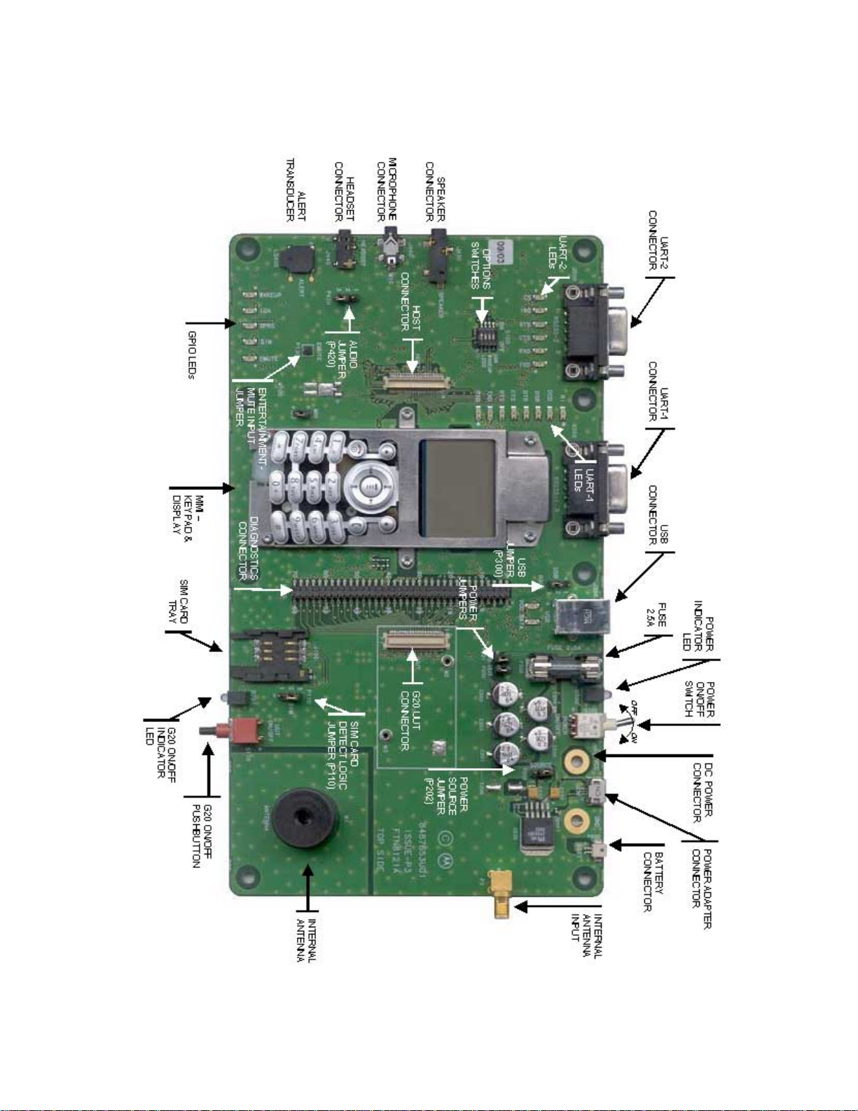
Figure 1 shows the Developer Board and some of its accessories with the g20 module attached to it: PLEASE PROVIDE
GRAPHIC.
98-08901C64-O 5
Figure 1. Developer Board with Accessories
Page 12

Developer Board and Interfaces Description
DRAFT 1 (31.3.03)
3.1.1 Developer Board Features
The Developer Board provides the following features to facilitate software and hardware development:
• Output of all g20 connector signals to a large header connector for debugging
• Host-systems connector
• AC, battery and DC power supplies for board operation
• LED indicators for critical signals
• Display and keypad for phone operation
• USB and RS232 serial interfaces
• Secondary RS232 interface using the SPI bus
• Digital audio interface
• Analog audio interface for speaker, alert speaker, microphone and headset
• SIM card connector
• Switches and jumpers for controlling board operation
6 98-08901C64-O
Page 13
3.1.2 Developer Board Connectivity
DRAFT 1 (31.3.03)
Figure 2 shows the Developer Board and its components:
Developer Board and Interfaces Description
98-08901C64-O 7
Figure 2. Developer Board Components
Page 14

Developer Board and Interfaces Description
DRAFT 1 (31.3.03)
3.1.3 Quick Start
This section describes a series of Quick Start procedures for first-time use of the Developer Board.
3.1.3.1 g20 Connection
Open the top cover of the Developer Board and insert the g20 in its designated position. The g20 should connect to the 70-pin
connector, labeled UUT (P1), and its holes should be aligned with the spacers on the Developer Board.
Fasten the g20 to the Developer Board spacers using two M2x0.4x6 mm screws provided with the kit. PLEASE PROVIDE
GRAPHIC.
Figure 3. Mounting the g20 Module
3.1.3.2 Antenna Connection
Connect the on-board antenna cable to the g20 antenna connector. Connect the RF Out output to the Internal antenna input using
the supplied cable. PLEASE PROVIDE GRAPHIC.
Figure 4. Attaching the RF Cable
Note
8 98-08901C64-O
While working, you can keep the box closed.
Page 15
Developer Board and Interfaces Description
DRAFT 1 (31.3.03)
3.1.3.3 Power Connection
The Developer Board can be powered using either a wall-mounted adapter, a DC power supply or a battery cell.
Only the adapter option is covered in this section. See “Power Connections” on page 15., when using other power
methods.
Note
Connect the adapter to the wall outlet and to the Developer Board adapter connector (J230) labeled Adapter.
The power source selection jumper, labeled Source, must be in the correct position for adapter operation (pins 1-2
shorted).
Note
3.1.3.4 Serial Connection
The USB and RS232 serial interfaces are available for PC communications. If a PC connection is required, connect either an
RS232 cable with a male D-Type connector to the labeled UART1 connector, or a USB cable with a B-Type connector to the
labeled USB connector.
When using a USB interface, be sure the USB jumper (P300) position reflects the g20 version being used. See
“USB” on page 11..
Note
3.1.3.5 Audio Connection
The Developer Board has several available audio configurations:
• Hands-free audio using the speaker and microphone
• Digital PCM audio
• Personal headset audio
Only the headset audio option is covered in this section. See “Audio Interface” on page 21. when using other audio
options.
Note
Connect the supplied headset to the headset connector (J440) labeled Headset.
3.1.3.6 SIM Card Connection
Insert a SIM card into the SIM tray (J100).
When using a SIM card, be sure the SIM jumper (P110) position reflects the g20 version being used. See “SIM
Card” on page 23. for more details.
Note
3.1.3.7 Default Switches and Jumper Settings
The Developer Board jumpers and switches are initially configured to comply with this Quick Start operation mode. If different
settings are necessary, refer to the relevant section for details about the required switch or jumper settings.
3.1.3.8 Operating the g20
After completing the initial setup, turn on the Developer Board power by switching the power switch (S200) to its on position,
and turn on the g20 by depressing the on/off switch (S110) or by depressing the on/off button on the keypad.
98-08901C64-O 9
Page 16
Developer Board and Interfaces Description
DRAFT 1 (31.3.03)
3.2 COMMUNICATIONS INTERFACES
The g20 Developer Board includes three different serial interfaces:
•RS232
•USB
• SPI
The RS232 and USB ports are multiplexed within the g20, and therefore cannot be operated simultaneously. Their default
connection is RS232. The SPI interface is used for debugging.
Each of these serial interfaces is described in the sections that follow.
3.2.1 RS232
The RS232 serial port is the primary interface to the g20 UUT via the J350 connector. This port is denoted by the RS232-1
marking beside the 9-pin, D-type connector.
The UUT RS232 signals are active-low CMOS-level signals (0-2.7 V), which are converted by the Developer Board to standard
RS232 levels for PC communications.
Table 2. RS232-1 Connector Pinout (J350)
Note
Pin # Description DTE I/O
1 DCD In
2RXD In
3TXD Out
4DTR Out
5 Ground
6DSR In
7RTS Out
8CTS In
9RI In
The RS232 connector pin names are DTE-oriented.
10 98-08901C64-O
Page 17
Developer Board and Interfaces Description
DRAFT 1 (31.3.03)
3.2.2 USB
The USB interface operates according to the g20 UUT configuration. The Developer Board has a complete USB transceiver
circuit to support USB communications for g20 units that do not include a USB driver of their own. The Developer Board USB
interface can be overridden manually when using a g20 unit that does include its own USB driver interface.
Table 3. USB Connector Pinout (J3)
Pin # Description
1VCC
2D-
3D+
4Ground
The USB jumper (P300) located next to the USB connector selects between the Developer Board USB interface and the UUT
USB interface. By changing the jumper position, the USB_VBUS signal is diverted to the selected driver (in the g20 or on the
Developer Board) and operates it.
Table 4. USB Selection (P300 Jumper)
P300
Jumper
Position
12 3
••
••
Selected Mode USB Source
g20 g20 driver
EVB (Developer Board) EVB driver
USB disconnected
3.2.3 SPI
The Developer Board includes a secondary 4-wire RS232 interface, which is connected to the g20 internal SPI bus through the
J500 connector. This interface is used to debug applications. This port is denoted by the RS232-2 label next to the 9-pin D-type
connector.
98-08901C64-O 11
Page 18
Developer Board and Interfaces Description
DRAFT 1 (31.3.03)
On the Developer Board, the g20 SPI interface is converted to standard RS232 signals for PC communications. The conversion
process uses the RS232 interface as a second slave on the internal g20 SPI bus, and communicates with it as such. SPI read and
write operations are performed normally, using the CS and IRQ signals provided by the conversion circuit. The IRQ signal is
connected to a g20 IRQ pin.
Table 5. RS232-2 Connector Pinout (J500)
Pin # Description DTE I/O
1Unused
2RXD In
3TXD Out
4Unused
5 Ground
6Unused
7RTS Out
8CTS In
9Unused
The RS232 connector pin names are DTE-oriented.
Note
3.3 CONNECTORS DESCRIPTION
All the Developer Board connectors are marked by their reference number and by a pin-1 indicator. Table 6 describes the available connectors on the Developer Board.
Table 6. Connectors
Reference Connector Description
P1 g20 UUT g20 UUT (unit under test) connector
J1 Host Emulates the g20 connector for host systems
12 98-08901C64-O
P100 Diagnostics Debug header connector (70-pin)
J300 USB USB B-type connector
J350 RS232-1 Primary RS232 to PC
J500 RS232-2 Secondary RS232 for debugging (SPI)
Page 19

Developer Board and Interfaces Description
DRAFT 1 (31.3.03)
Table 6. Connectors (Continued)
Reference Connector Description
J430 Speaker Hands-free system speaker jack
J460 Microphone Hands-free system microphone jack
J440 Headset Headset jack
J201 VCC Developer Board DC power supply
J200 GND Developer Board common ground
P600 Battery Battery connector
J230 AC adapter/charger Wall-mount adapter connector (CE bus
compatible)
J100 SIM card SIM card socket with detection
P2 Antenna connector SMA connector for g20 antenna
M1 RF Antenna RF antenna
DS800 Display Display pads
3.3.1 UUT Interface Connector
Table 7 lists the pin names and functions available for g20 interface connectors. All pin numbers and functions are identical for
the P1, J1 and P100 connectors on the Developer Board.
Table 7. g20 Connectors Pinout
Pin # Pin Name Pin # Pin Name
1 GND 2 GND
3 GND 4 GND
5 VCC 6 VCC
7 VCC 8 VCC
98-08901C64-O 13
9 RTS_N 10 USB_DET
11 RXD_N 12 Not connected
13 DSR_N 14 Not connected
15 CTS_N 16 WAKEUP_IN_N
Page 20

Developer Board and Interfaces Description
DRAFT 1 (31.3.03)
Pin # Pin Name Pin # Pin Name
17 DCD_N 18 PCM_DIN
19 DTR_N 20 PCM_DOUT
21 TXD_N 22 PCM_CLK
23 RI_N 24 PCM_FS
25 RESET_N 26 WAKEUP_OUT_N
27 BL_SINK 28 KBC1_N
29 CHRG_DIS 30 KBC0_N
31 CHRG_SW 32 KBR0_N
33 CHRG_STATE 34 KBR1_N
Table 7. g20 Connectors Pinout (Continued)
35 CHRG_DET_N 36 KBR2_N
37 ENT_MUTE 38 KBR3_N
39 TX_EN_N 40 KBR4_N
41 ANT_DET 42 KBR5_N
43 VIB_OUT 44 SIM_RST_N
45 CHRG_TYP 46 SIM_CLK
47 THERM 48 SIM_VCC
49 GPRS_DET_N 50 SIM_PD
51 IGN 52 SIM_DIO
53 ON_OFF_N 54 LCD_CS
55 HDST_INT_N 56 LCD_DATA
57 HDST_MIC 58 LCD_CLK
14 98-08901C64-O
59 MIC_GND 60 LCD_RS
61 MIC 62 SPI_IRQ_N
63 ALRT_N 64 SPI_DIN
Page 21

Developer Board and Interfaces Description
DRAFT 1 (31.3.03)
Table 7. g20 Connectors Pinout (Continued)
Pin # Pin Name Pin # Pin Name
65 ALRT_P 66 SPI_CLK
67 SPKR_N 68 SPI_DOUT
69 SPKR_P 70 SPI_CS
3.4 POWER CONNECTIONS
Developer Board power can be supplied from a DC power source, an AC power adapter or a battery. The same power source is
used for the UUT and the board peripherals.
The Developer Board includes three jumpers for controlling the power supply:
• P202: AC adapter or battery power source selection
• P201: Connects/disconnects the Developer Board peripherals from the power supply
• P200: Connects/disconnects the g20 from the power supply
Each power supply option is described in the sections that follow.
3.4.1 DC Power Source Operation
When using a DC power supply, the power source is applied to connectors J201 (VCC) and J200 (Ground). The DC voltage
applied through this connection should not exceed the recommended operational limits of 3V-4.2V. In all cases, the DC source
input is protected from over voltage and reverse polarity, and includes a 2.5A protective fuse.
The supplied DC input connectors must be attached to the Developer Board in order to use the DC power source. The two
connectors should be screwed into their appropriate positions (J201, labeled VCC, and J200, labeled GND). Use the red connector for VCC and the black one for GND. Connect the DC power source to these connectors using banana plugs, alligator clamps
or wire.
It is recommended to remove jumper P202 when using the DC power source. In any case, the DC power source
should not be used when other sources are connected.
!
Caution
98-08901C64-O 15
Page 22

Developer Board and Interfaces Description
DRAFT 1 (31.3.03)
3.4.2 AC Adapter Operation
When using an AC adapter, the adapter is connected to J230. The adapter supplies a constant 4.5 V, which is regulated to a
nominal 4.1 V on the Developer Board.
Table 8. J230 Connector Pinout
Pin # Pin Name
1GND
2 Detection circuit
3VCC
3.4.3 Battery Operation
The Developer Board supports a battery power supply. The battery used must be a 3.6V lithium-ion cell, corresponding to
Motorola part number 0189727L01.
When using a battery as the main power source, the AC adapter input operates as a battery charger, which connects to an
on-board battery charging circuit.
Table 9. P600 Connector Pinout
Pin # Pin Name
1VCC
2GND
3.4.4 Power Source Selection
The Developer Board AC adapter and battery power inputs include a selection jumper (P202) that diverts either the regulated
AC adapter power or the battery power to the board.
Table 10. Power Source (P202 Jumper)
P202 Jumper
Position
12 3
Selected Mode Power Source
16 98-08901C64-O
••
••
Adapter AC Adapter
Battery LiIon Battery
Adapter and battery disconnected DC power only
Page 23

The DC power source input is independent of the other power inputs, and does not pass through this selection
DRAFT 1 (31.3.03)
jumper. Nevertheless, it is still recommended to disconnect the P202 jumper when using the DC source.
Note
3.5 SWITCHES AND JUMPERS
Table 11 describes the available switches and jumpers on the Developer Board.
Table 11. Switches and Jumpers
Reference Switch/Jumper Description
S200 Board on/off Developer Board on/off switch
S110 g20 on/off g20 UUT on/off push button switch
S100 Options switch Four switches for Developer Board options
P420 Audio Analog/digital audio-selection jumper
Developer Board and Interfaces Description
P201 EVB Peripheral power input jumper
P200 UUT g20 UUT power input jumper
P202 Source Power source selection jumper
P110 SIM SIM card detect logic selection jumper
P300 USB USB driver source selection jumper
P130 EMUTE Entertainment mute connection point
98-08901C64-O 17
Page 24

Developer Board and Interfaces Description
DRAFT 1 (31.3.03)
3.6 LED INDICATORS
Table 12 describes the LED indicators available on the Developer Board. Each LED is marked on the board by the function it
represents.
Table 12. LED Indicators
Group LED Reference Description
WAKEUP D704 Wake-up in/out
IGN D702 Ignition input
GPRS D710 GPRS coverage indication
GPIO
SPI
USB
RS232-1
SIM D703 SIM card reset indication
UUT D701 g20 reset signal
PWR D200 Developer Board power indicator
EMUTE D708 Entertainment mute indicator
CS D741 SPI chip-select output
IRQ D745 SPI IRQ input
VCC D760 USB VBUS
DATA D761 USB D+
RXD D722 DTE receive data
TXD D721 DTE transmit data
RTS D724 Request to send
CTS D723 Clear to send
DTR D725 Data terminal ready
18 98-08901C64-O
DSR D726 Data set ready
DCD D727 Carrier detect
RI D728 Ring indicator
Page 25

Developer Board and Interfaces Description
DRAFT 1 (31.3.03)
Table 12. LED Indicators (Continued)
Group LED Reference Description
RXD D743 DTE receive data
TXD D742 DTE transmit data
RS232-2
CTS D744 Clear to send
RTS D745 Request to send
3.7 MMI
The Developer Board includes a man-machine interface (MMI), complete with display and keypad. The signals from the display
and keypad are directly connected to the UUT interface.
3.7.1 Display
The grayscale display (DS800) is not a standalone component, and includes a complete assembly in which it is housed, along
with other necessary parts.
Table 13. Display Connector Pinouts (DS800)
Pin # Description
1Chip select
2Reset
3 Register select
4 Serial clock
5 Serial data
6 Supply
7 Supply
8Ground
9Vout
98-08901C64-O 19
Page 26

Developer Board and Interfaces Description
DRAFT 1 (31.3.03)
3.7.2 Keypad
Table 14 describes the Developer Board keypad layout.
Table 14. Keypad Functions
Pad Reference Function Alternate
S803 1 Punctuation
S802 2 ABC
S820 3 DEF
S801 4 GHI
S805 5 JKL
S804 6 MNO
S806 7 PQRS
S817 8 TUV
S811 9 WXYZ
S809 0 +
S810 Star (*)
S815 Pound (#)
S814 Send
S813 End On/Off
S819 Menu
S822 Right
S823 Left
S818 Up
S816 Down
20 98-08901C64-O
S812 Soft Right
S808 Soft Left
Page 27

Developer Board and Interfaces Description
DRAFT 1 (31.3.03)
3.8 AUDIO INTERFACE
The Developer Board includes analog and digital audio interfaces. The audio interface contains a hands-free speaker and microphone, a headset, and an alert speaker.
3.8.1 Speaker
The differential speaker interface is designed as a car-kit hands-free speaker. The Developer Board uses an audio amplifier to
amplify the speaker audio output to desired levels. The speaker connector (J430) is labeled SPEAKER. The speaker output is 8
ohms matched.
Table 15. Speaker Connector Pinout (J430)
Pin # Description
1 Not connected
2 Speaker positive output
3 Speaker negative output
4 Not connected
3.8.2 Microphone
The microphone interface is designed as a car-kit hands-free microphone. The microphone connector (J460) is labeled MIC.
Table 16. Microphone Connector Pinout (J460)
Pin # Description
1Ground
2 Microphone audio-in
3Ground
4Ground
5Ground
3.8.3 Audio Source Selection
Microphone and speaker audio can be routed through two different sources: the g20 audio amplifiers or the g20 digital audio
interface. The Developer Board includes a CODEC that converts the g20 digital audio data to analog audio signals.
98-08901C64-O 21
Page 28

Developer Board and Interfaces Description
DRAFT 1 (31.3.03)
The P420 jumper selects the speaker and microphone source, as indicated in Table 17.
Table 17. Audio Source (P420 Jumper)
P420 Jumper
Position
12 3
••
••
Selected Mode Audio Source
Digital audio CODEC audio I/O
Analog audio G20 audio I/O
Audio disconnected
3.8.4 Headset
The headset interface is designed as a portable phone audio interface, and is similar to the headset interface. The headset connector (J440) includes a speaker, microphone and a detection signal. The speaker and microphone signals are directly connected to
the g20 audio signals.
The purpose of the detection circuit is to switch the g20 headset audio paths on and off, whenever a headset connection is
detected. Headset detection is made whenever a headset plug is inserted into the jack. This action disables the g20 microphone
and speaker, and routes the audio signals to the headset.
Table 18. Headset Connector Pinout (J440)
Pin # Description
1 Ground
2 Headset-detect switch
3 Speaker audio-out
4 Microphone audio-in
5 Ground
22 98-08901C64-O
Page 29

Developer Board and Interfaces Description
DRAFT 1 (31.3.03)
3.8.5 Alert Speaker
The Developer Board includes an on-board transducer for alert audio sounds (LS400), which is labeled ALERT. The transducer
is connected directly to the g20 differential alert outputs. The alert transducer is similar to the alert speaker, which sounds the
g20 MIDI signals.
Table 19. Alert Transducer Pinout (LS400)
Pin # Description
1 Alert audio inverted output
2 Alert audio positive output
3 Alert audio inverted output
4 Alert audio inverted output
3.9 DEVELOPER BOARD PERIPHERALS
This section describes the connectors for peripheral devices that can be used with the Developer Board.
3.9.1 SIM Card
The SIM card connector (J100) is external to the UUT, but is connected directly to it, similar to an internal SIM. The UUT can
accept 1.8V and 3V SIM cards.
Table 20. SIM Connector Pinouts (J100)
Pin Description
1Ground
2 Presence detect
3Clock
4Reset
5VCC
6 Serial data I/O
7 VPP
8Ground
98-08901C64-O 23
Page 30

Developer Board and Interfaces Description
DRAFT 1 (31.3.03)
The SIM card supports both active-high and active-low detection configurations. Jumper P110 is used to select between these
configurations.
Table 21. SIM Detection Logic (P110 Jumper)
P110 Jumper
Position
12 3
••
••
Selected Mode
Active-low
Active-high
Not active
3.9.2 Entertainment Mute
The Developer Board includes an entertainment-mute logic circuit that is responsible for muting a car radio whenever the phone
is in use (for example, incoming calls, dialing, and so on).
The entertainment-mute logic circuit includes an ENABLE input that is both a g20 signal and an open-collector MUTE output.
This circuit is connected to jumper P130 for host systems.
The entertainment-mute operation is not currently supported by the g20.
Note
3.9.3 LEDs Logic and Control
The Developer Board includes LED indicators for critical signals. A 3.0V regulator powers the LEDs, and an on/off switch
controls their operation. The switch is located in the S100 switch array, and is labeled LED. Turning the switch on and off
enables or disables all LED activity, respectively.
The Developer Board power LED and the g20 on/off LED are always active and cannot be disabled.
3.9.4 ADC Test Logic
The g20 has two ADC pins. The g20 charger and temperature monitor currently occupy these pins. The Developer Board
includes optional resistors for ADC testing. These resistors, two for each ADC signal, can be used to set a specific voltage across
the ADC signal.
24 98-08901C64-O
Page 31

Developer Board and Interfaces Description
DRAFT 1 (31.3.03)
The G20 has a 47K-ohm internal pull-up resistor at each ADC input, as shown in Figure 5.
Figure 5. ADC Test Logic
3.9.5 Ignition
The Developer Board contains an on/off switch that is connected to the g20 UUT ignition circuit. The switch is located in the
S100 switch array, and is labeled IGN. Turning the switch on applies the UUT supply on the Ignition input pin.
3.9.6 Wakeup
The Developer Board includes a wakeup switch that toggles the g20 WAKEUP_IN_N signal. The switch is located in the S100
switch array, and is labeled WAKEUP.
3.9.7 AC Adapter Detection Circuit
The g20 charger module includes a detection logic circuit for detecting charger presence and type. The detection circuit is internal to the g20 module. However, the Developer Board does contain the necessary routing from the g20 UUT to the AC adapter
connector.
Two g20 signals are used for this detection:
• AD1: ADC signal for charger type detection
• CHRG_SW: Charger rate control
These detection signals are present to provide compatibility with the phone. They may be removed in future versions.
3.10 ANTENNA CONFIGURATION
An antenna (internal or external) must be connected to the Developer Board for adequate GSM reception. You can connect the
g20 to either the on-board internal antenna or to an external antenna. Two RF connectors on the Developer Board, labeled INT
ANT and EXT ANT, are used for this purpose. The EXT ANT connector has an internal extension cable with MMCX termination, which must be connected to the g20 RF connector. The INT ANT connector is an on-board connection to the Developer
Board internal antenna.
When using the internal antenna option, the additional RF cable supplied in the Developer’s Kit must be connected between the
EXT ANT and INT ANT connectors. When using the external antenna option, an external antenna or antenna application must
be connected to the EXT OUT connector. (The connection cable is not included.)
98-08901C64-O 25
Page 32

Developer Board and Interfaces Description
DRAFT 1 (31.3.03)
3.11 TEST POINTS
Table 22 describes the available test points on the Developer Board.
Table 22. Test Points
Reference Function
TP400 Alert speaker positive signal
TP401 Alert speaker inverted signal
3.12 ELECTRICAL SPECIFICATIONS
Table 23 describes the electrical specifications OF the Developer Board.
Table 23. Electrical Specifications
Parameter Min Typ Max Units
DC power supply 3.0 3.6 4.2 V
Adapter power supply 4.4 4.6 12 V
Battery power supply 3.0 3.6 4.2 V
Off current --- 36 46 uA
On current 8.1 8.33 8.45 mA
Active current peripherals off 12.7 13 --- mA
Active current peripherals on
* 13.1 --- 190 mA
*
Depends on the active peripherals (LEDs, UART, USB, and so on) in use.
26 98-08901C64-O
Page 33

4. MECHANICAL DESCRIPTION
DRAFT 1 (31.3.03)
4.1 MECHANICAL REQUIREMENTS FOR MOUNTING THE G20 MODULE
The size of the g20 module is 45.2 x 24.4 x 6 mm. Two 2.4 mmØ holes are provided to accommodate M2 screws or #1-64 UNC
2A machine screws. Torque to 2 inches per pound. Refer to Figure 6 below for mounting requirements:
98-08901C64-O 27
Figure 6. Mechanical Mounting Requirements
Page 34

Mechanical Description
DRAFT 1 (31.3.03)
28 98-08901C64-O
Page 35

5.1 WEB PAGES
DRAFT 1 (31.3.03)
PLEASE PROVIDE DETAILS FOR THIS SECTION.
5.2 CUSTOMER ASSISTANCE
For customer assistance, contact us as directed below:
Helpdesk email: n2cshd@motorola.com
Helpdesk telephone: +972-3-568-4040
5. SERVICE SUPPORT
98-08901C64-O 29
Page 36

Service Support
DRAFT 1 (31.3.03)
30 98-08901C64-O
Page 37

6. SCHEMATICS, PLACEMENT AND
DRAFT 1 (31.3.03)
6.1 SCHEMATICS
This section presents the schematics for the g20 Developer Board.
PLEASE PROVIDE INFORMATION FOR FIGURE CAPTIONS.
PARTS LIST
98-08901C64-O 31
Page 38

Schematics, Placement and Parts List
DRAFT 1 (31.3.03)
32 98-08901C64-O
Figure 7.
Page 39

Schematics, Placement and Parts List
DRAFT 1 (31.3.03)
98-08901C64-O 33
Figure 8.
Page 40

Schematics, Placement and Parts List
DRAFT 1 (31.3.03)
34 98-08901C64-O
Figure 9.
Page 41

Schematics, Placement and Parts List
DRAFT 1 (31.3.03)
98-08901C64-O 35
Figure 10.
Page 42

Schematics, Placement and Parts List
DRAFT 1 (31.3.03)
36 98-08901C64-O
Figure 11.
Page 43

Schematics, Placement and Parts List
DRAFT 1 (31.3.03)
98-08901C64-O 37
Figure 12.
Page 44

Schematics, Placement and Parts List
DRAFT 1 (31.3.03)
38 98-08901C64-O
Figure 13.
Page 45

Schematics, Placement and Parts List
DRAFT 1 (31.3.03)
98-08901C64-O 39
Figure 14.
Page 46

Schematics, Placement and Parts List
DRAFT 1 (31.3.03)
40 98-08901C64-O
Figure 15.
Page 47

6.2 DEVELOPERS BOARD PLACEMENT
DRAFT 1 (31.3.03)
Figure 16 shows the top layout of the Developer Board:
Schematics, Placement and Parts List
98-08901C64-O 41
Figure 16. Developer Board Top Layout
Page 48

Schematics, Placement and Parts List
DRAFT 1 (31.3.03)
Figure 17 shows the bottom layout of the Developer Board:
42 98-08901C64-O
Figure 17. Developer Board Bottom Layout
Page 49

6.3 DEVELOPER BOARD PARTS LIST
DRAFT 1 (31.3.03)
Table 24. Developer Board Parts List
Schematics, Placement and Parts List
REFERENCE
SYMBOL
R440 0662057A21 RES, 68
R600 0662057A22 RES, 75
R330 0662057A25 RES, 100
R773 0662057A28 RES, 130
R723, R725,
R745, R747
R703 0662057A35 RES, 270
R705, R707,
R709-10,
R713,
R717-18,
R727, R729,
R731, R733,
R735, R737,
R743, R749,
R751, R753,
R763, R764
R203 0662057A39 RES, 390
R603 0662057A47 RES, 820
R604 0662057A49 RES, 1K
R602 0662057A51 RES, 1.2K
R312 0662057A53 RES, 1.5K
R465-66 0662057A57 RES, 2.2K
R201-2, R702,
R704, R706,
R708,
R711-12,
R716, R722,
R724, R726,
R728, R730,
R732, R734,
R736, R742,
R744, R746,
R748, R750,
R752,
R760-61,
R800
R179, R197,
R200, R303,
R414-16,
R441, R508-9,
R525, R601,
R607, R774,
R781
R230-32,
R322
MOTOROLA
PART NO.
Resistors
0662057A31 RES, 180
0662057A36 RES, 300
0662057A65 RES, 4.7K
0662057A73 RES, 10K
0662057A75 RES, 12K
DESCRIPTION
98-08901C64-O 43
Page 50

Schematics, Placement and Parts List
DRAFT 1 (31.3.03)
Table 24. Developer Board Parts List (Continued)
REFERENCE
SYMBOL
R411-12,
R418
R177-78,
R191-92,
R196, R198,
R317-18,
R320-21,
R353, R507,
R608-9, R780
R435 0662057A97 RES, 100 K
R1, R10-11,
R15-16, R107,
R116-144,
R146,
R148-49,
R151-53,
R155, R157,
R159, R170,
R172-76,
R181-190,
R300-302,
R350-352,
R400-402,
R407-410,
R413, R417,
R419,
R423-27,
R460,
R480-85,
R500-503,
R506,
R510-524,
R594-97,
R606,
R611-618,
R700, R720,
R740,
R770-771,
R801-805
R790 0662057C01 RES, 0
R430-31,
R433-34
R221 0662057P95 RES, 100K
R234 0662057P96 RES, 130K
R211, R220,
R241
R210, R240 0662057P99 RES, 200K
R233 0662057T17 RES, 301K
R310-11 0662057T43 RES, 33.2
R772 0662057W13 RES, 3.3
MOTOROLA
PART NO.
0662057A80 RES, 20 K
0662057A89 RES, 47 K
0662057B47 RES, 0
0662057P20 RES, 20K
0662057P97 RES, 150K
DESCRIPTION
44 98-08901C64-O
Page 51

Table 24. Developer Board Parts List (Continued)
DRAFT 1 (31.3.03)
Schematics, Placement and Parts List
REFERENCE
SYMBOL
F200 0904923K01 FUSE
F600 6586221J04 FUSE
J430 0909032K01 CONN_J
J460 0909399T09 CONN_J
J350, J500 0909672B03 CONN_J
P2 0909908P02 CONN_J
J1 0987547V01 CONN_J
J300 0987583U01 CONN_J
J440 0987837L02 CONN_J
J230 0989601K01 CONN_J
C1, C2, C3, C42113740F01 CAP, 0.5p
C5 2113740F19 CAP, 4.7p
C207, C215,
C217, C234
C442, C444,
C447, C450,
C462,
C472-473
C100,
C102-106,
C108-115,
C130, C137,
C143,
C147-151,
C153-160,
C171,
C191-192,
C211, C221,
C241, C312,
C401-404,
C416-418,
C421-428,
C436-439,
C443,
C445-446,
C448-449,
C451-2, C461,
C463-4,
C470-471,
C474-475,
C502-510,
C781,
C810-819
MOTOROLA
PART NO.
Fuses
Connectors
Capacitors
2113740F25 CAP, 8.2p
2113740F27 CAP, 10p
2113740F39
DESCRIPTION
CAP, 33p
98-08901C64-O 45
Page 52

Schematics, Placement and Parts List
DRAFT 1 (31.3.03)
Table 24. Developer Board Parts List (Continued)
REFERENCE
SYMBOL
C125, C128,
C131, C134,
C208, C216,
C218, C231,
C511-12
C411-412,
C414
C101, C107,
C116-124,
C126-127,
C129,
C132-133,
C135-136,
C138-142,
C144-146,
C152, C465,
C600
C430-431,
C433-434
C361-364,
C521-524
C310, C313,
C466
C440-441 2113928C12 CAP, 10u
C170,
C172-173,
C180, C190,
C200, C233,
C300, C311,
C350, C360,
C400, C410,
C413, C415,
C420, C432,
C435, C453,
C460, C500,
C513, C520,
C700, C720,
C770-774,
C780,
C800-801
C230, C232 2311049A57 CAPP, 10u
C210, C212,
C220, C222,
C240, C242
C201-206 2387572V01 CAPP, 1000u
L440 2409154M42 IDCTR, 33n
SH400 2604044K01 SHIELD
MOTOROLA
PART NO.
2113740F41 CAP, 39p
2113741F49 CAP, 10n
2113743E20 CAP, 100n
2113743K16 CAP, 220n
2113743K17 CAP, 330n
2113928C04 CAP, 4.7u
2113928P04 CAP, 1u
2311049A72 CAPP, 10u
Inductors
Shields
DESCRIPTION
46 98-08901C64-O
Page 53

Table 24. Developer Board Parts List (Continued)
DRAFT 1 (31.3.03)
Schematics, Placement and Parts List
REFERENCE
SYMBOL
P130 2880001R01 CONN_P
P120,
P200-201
P110, P202,
P300, P420
P600 2886290J07 CONN_P
P100 2886397J02 CONN_P
P1 2887548V01 CONN_P
J201 2987604U01 CONN_J
J200 2987604U02 CONN_J
M1 3903920K01 CONTACT
S200 4008241G06 SWITCH_ET01
S110 4008242G05 SWITCH
J100 4009060S03 SWITCH_CONTACT_BLOCK
S100 4080564C02 SWITCH
M2, M3, M4,
M5, M6, M7,
M8, M9
D702-704,
D708, D710,
D721-8,
D741-746,
D760-761
D770-771 4870370A25 CL-260S-WA
D200, D701 4880304L02 LED_RED
Q701-704,
Q706, Q708,
Q710,
Q760-761
Q705, Q707,
Q711,
Q721-728,
Q741-746
Q200, Q780
Q350, Q720,
Q740, Q1000
MOTOROLA
PART NO.
Connectors
2880001R02 CONN_P
2880001R03 CONN_P
Contacts
Switches
Spacers
4302809C15 SPACER
LEDs
4805729G44
Transistors
4809579E16 TN0200T
4809579E18 TP0101T
4809807C31
4809939C05
DESCRIPTION
BR1102W
IRF7220
UMC5NTL
98-08901C64-O 47
Page 54

Schematics, Placement and Parts List
DRAFT 1 (31.3.03)
Table 24. Developer Board Parts List (Continued)
REFERENCE
SYMBOL
Q110, Q300,
Q500, Q610,
Q620, U771
Q201
Q600
Q190
VR200
D320 4813833C02 MMBD6100
VR100-105,
VR310
U510 5102870C15 MAX3100EEE
U201, U220,
U240
U230 5104187K89 MIC29302BU
U370, U380,
U530
U520 5108428S67 MAX3223EAP
U330 5109522E53 NC7SZ125
U360 5109781E76 MAX3238
U320 5109817F26 TC54VN2902E
U420 5113805B39 MC74HC4053
U410 5113811A56 MC145481
U300, U350,
U400, U500
U430 5186214J87 TPA6203A1GQVR
U600 5187970L09 LM3652
U310 5187970L15 ISP1104
U770 5187970L20 LM2795BLX
M100 5987772L02 MOTOR
Y510 4884450T02 XTAL3_6864MHZ
LS400 5087951K01 SPKR
MOTOROLA
PART NO.
4813824A10
4813824A17
4813824B11
4813824B13
Diodes
4813831A14
4886182U05 UMZ6.8EN
Integrated Circuits
5104187K10 MAX604ESA
5105492X05 TC7SH32
5113837A07 MC74LCX244
General
DESCRIPTION
MMBT3904
MMBT3906
MMJT9435
MMJT9410T1
SMB5918
48 98-08901C64-O
Page 55

7. ERRATA
DRAFT 1 (31.3.03)
7.1 SWITCH ASSIGNMENTS CORRECTION
The S100 options switch on the Developer Board is labeled incorrectly. Figure 18 shows the correct function of each switch.
PLEASE PROVIDE A PICTURE WITHOUT CALLOUTS.
Figure 18. S100 Options Switch Functions
98-08901C64-O 49
Page 56

Errata
DRAFT 1 (31.3.03)
50 98-08901C64-O
Page 57

8. INDEX
DRAFT 1 (31.3.03)
98-08901C64-O 51
Page 58

Index
DRAFT 1 (31.3.03)
52 98-08901C64-O
 Loading...