

Page 1

Developers Manual
Abc
APPLICANT: MOTOROLA INC. FCC ID: IHDT56CW1
EXHIBIT 8
rev. X1 draft 142
9808901C64
23 February 2003
c18 DEVELOPERS KIT MANUAL
A preliminary draft copy of the Users Manual follows:
1
Page 2

Abc
Developers Manual
rev. X1 draft 142
9808901C64
23 February 2003
c18 DEVELOPERS KIT MANUAL
2
Page 3

Developers Manual
Abc
rev. X1 draft 142
9808901C64
23 February 2003
Preface
Scope of this Manual
Data terminal equipment (DTE) OEM teams are often pulled together quickly from other work
groups.
For this reason, OEM team members often need advice about how to best sustain a concerted
design
And development effort. The goal of this guide is to assist the team to successfully produce a
ireless
Product that integrates a Motorola c18 wireless modem.
Who Should Use This Manual
Our readers are intended to be data terminal equipment (DTE) OEM integration team members.
Teams historically consist of representative from the disciplines of hardware, software, and RF
engineering.
Disclaimer
This guide provides advice and guidelines to OEM teams. Responsibility for how the information
is
Used lies entirely with the OEM. Statements indicating support provided by or offered by Motorola
are subject to change at any time. Motorola reserves the right to make any changes to this
specification.
Regulatory Requirements
The Federal Communications Commission (FCC) requires application for certification of digital
devices in accordance with CFR Title 47, Part 2 and Part 15. This includes Electromagnetic
Energy
Exposure (EME) testing. As the c18 modem is not a stand alone transceiver but is an integrated
module, the c18 cannot be tested by itself for EME certification. It is, however, the integrator
responsibility to have the completed device tested for EME certification.
Regulatory Statement
The following safety precautions must be observed during all phases of the operation,
usage, service or repair of any cellular terminal or mobile incorporating c18 module.
Manufacturers of the cellular terminal are advised to convey the following safety
information to users and operating personnel and to incorporate these guidelines into all
manuals supplied with the product. Failure to comply with these precautions violates
safety standards of design, manufacture and intended use of the product. Motorola
assumes no liability for customer failure to comply with these precautions.
1. The c18 must be operated at the voltages described in the technical documentation.
3
Page 4

Developers Manual
Abc
2. The c18 must not be mechanically nor electrically changed. Usage of connectors should follow
the
guidance of the technical documentation.
3. The c18 has been designed the meet the EMC requirements of ETS 300 342.
4. When integrating the c18 into a system, Motorola recommends testing the system to
ETS300342-1.
5. The c18 meets the safety requirements of EN60950.
6. Systems using the c18 will be subject to mandatory EMC testing under directive 89/336/EEC
and
only optional (see 3.) Other directives like the LVD directive 73/23/EEC might also be applicable
to a
system using c18.
rev. X1 draft 142
9808901C64
23 February 2003
4
Page 5

Developers Manual
Abc
Safety
rev. X1 draft 142
9808901C64
23 February 2003
User Operation
Do not operate your telephone when a person is within 8 inches (20 centimeters) of the antenna.
A person or object within 8 inches (20 centimeters) of the antenna could impair call quality and
may cause the phone to
to
RF energy in excess of that established by the FCC RF Exposure Guidelines.
IMPORTANT: The telephone must be installed in a manner that provides a minimum separation
Distance of 20 cm or more between the antenna and persons to satisfy FCC RF exposure
requirements for mobile transmitting devices.
IMPORTANT: To comply with the FCC RF exposure limits and satisfy the categorical exclusion
requirements for mobile transmitters, the following requirements must be met.
Antenna Installation
1. A minimum separation distance of 20 cm must be maintained between the antenna and all persons.
2. The transmitter effective radiated power must be less than 1.5 Watts ERP (2.45 Watts or 33.9 dBm EIRP).
This requires that the combination of antenna gain and feed line loss does not exceed 6.1 dBi.
operate at a higher power level than necessary and expose that person
Applicable Documents
c18 Cellular Engine Module Description - 9808901C63
Arrangement of this Manual
5
Page 6

Developers Manual
Abc
rev. X1 draft 142
9808901C64
23 February 2003
Introduction
General Description
c18 Developer’s Kit (F4441A) is intended for developing and testing software applications for c18
module, as well as for c18 evaluation. Developer’s kit can accommodate different c18 models –
with different interfaces (i.e. full featured 70 pin interface connector, 36 pin ZIF connector and
28 pin DIN connector).
Terms and Abbreviations
Acronyms / Terms Definition / Description
1X Platform 1X
ACK Acknowledgement from the radio that the test command was successful
ADB Application Development Board (old name for Developer Board)
AGND Audio Ground
BOM Bill of Materials
c18a Full c18 OEM model
c18c c18 CDMA800 only model
CDMA Code Division Multiple Access
ESD Electro-Static Discharge
GHz Gigahertz
GND Electrical Ground
KHz Kilohertz
LPF Low Pass Filter
mA Milliamp
MHz Megahertz
N/A Not Applicable
NC Not Connected
PA Power Amplifier
PCS Personal Communications System
PCS PCS Band. Also known as CDMA 1900
RF Radio Frequency
R-UIM Removable User Identity Module
SW Software
TBD To Be Determined
ZIF Zero Insertion Force
Safety Precautions
Majority of the Developer’s Board circuits are not shielded. Take maximum precaution measures
to avoid ESD. ESD may damage Developer’s Board and/or c18 module attached to it.
6
Page 7
Developers Manual
Abc
rev. X1 draft 142
9808901C64
23 February 2003
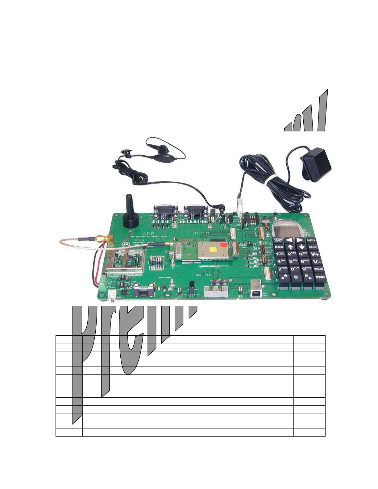
Developer Board and Interfaces Description
General
The Developer Board is the main part of the Developer’s Kit. It serves as a mounting platform for
c18 module. It provides c18 with supply voltage and provides a user with standard
communication interfaces (USB and RS232).
A picture of Developer Board with some of its accessories and c18 attached to it is shown below:
GETTING STARTED (USING THE DEVELOPER’S KIT)
Developer’s Kit contents:
Item # Item Description Part Number Quantity
1 c18a FTN8125A 1
2 Developer’s Board FTN8126A 1
3 Power Supply SPN4716B 1
4 Euro Adapter Plug SYN7456A 1
5RS232 Cable 1
6USB Cable 1
7 RF Cable 3087563V05 2
8 Documentation and Driver Bundle CD FTN6246A 1
9 Nut M2x0.4 0280349L02 4
10 Antenna 8509397T03 1
11 Spare 1.6A Fast-Acting Fuse 6502069C48 1
12 Spare Jumper 0984181L01 1
7
Page 8

Developers Manual
Abc
13 Headset SYN8419B 1
14 Microphone SMN4020B 1
15 36 Lead Flex Cable 50mm 3086229J10 1
16 70 lead Flex cable (option)
17 70 lead Flex cable (option)
rev. X1 draft 142
9808901C64
23 February 2003
System requirements
· Personal Computer
· Available COM port
· Available USB 2.0 (full-speed) port
· Available RS232 ports
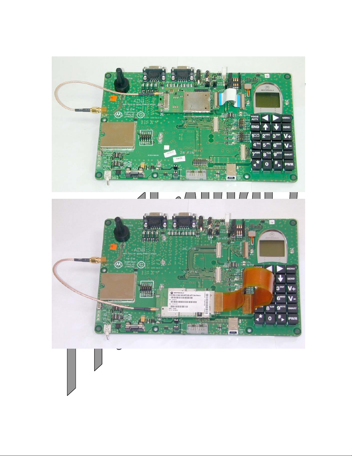
Hardware Setup
Mount the c18 module supplied with the kit on the supporting spacers and plug it into the
matching connector on the Developer’s Board. Secure the module using two M2x0.4 nuts
provided in the kit (other two nuts are spare). There are three possible configurations, shown in
the following pictures:
For users using the fully featured 70 pin interface:
For users using the 36 ZIF connector interface:
8
Page 9
Abc
Developers Manual
rev. X1 draft 142
9808901C64
23 February 2003
For users using the 28pin DIN connector interface:
Plug the RF cable (3087563V05) into the Developer’s Board and then to c18 module. Attach the
headset supplied to headset connector on the Developer’s Board. Mount the Antenna onto the
Antenna Base (M601) on the Developer’s Board.
Connect the desired communications cable between a PC and the Developer’s Board (RS232 or
USB). If RS232 cable is used, connect the RS232 cable to connector marked J210 and UART1.
9
Page 10

Developers Manual
Abc
Connect the Power supply provided in the kit to Developers Board Power Connector J500. Plug
the Power Supply into the mains.
Power-up
Switch the Power switch S500 into the “ON” position. This will turn some of the Developer’s
Board LEDs on. At this point, Developer’s Board is on, and c18 module has voltage supply. The
c18 module will remain off and LCD will remain blank.
To turn the module on, press on the keypad key “PWR” for at least 2 seconds to turn the module
on.
rev. X1 draft 142
9808901C64
23 February 2003
10
Page 11

Developers Manual
Abc
rev. X1 draft 142
9808901C64
23 February 2003
Configuring Communication Mode
The c18 module will enter the USB communications mode when it’s powered up, no configuration
switches are closed and a USB cable connects the Developer’s Board with an active USB port on a
PC.
In order to choose RS232 mode, make sure RS232 cable is properly connected to the Developer’s
Board and a PC. Move the S101 “OPT1” configuration switch to closed position.
Note: Configuration Switches have a small mark “ON” printed on them. When a
switch tab is in “ON” mark direction, the switch is “Closed”. When it is in the opposite
direction of the mark, the switch is “Open”.
For detailed description of configuration switches setting and available modes, please refer to
chapter x.x “CONFIGURATION SWITCHES DESCRIPTION”.
11
Page 12

Developers Manual
Abc
Testing the installation
Once the hardware setup has been completed, you may test the communication with the
module.
RS232 communication:
Below is an example of a setup needed for HyperTerminal in order to communicate with the
module.
rev. X1 draft 142
9808901C64
23 February 2003
USB Communication: TBD
12
Page 13

Abc
Developers Board Description
DEVELOPER BOARD CONNECTOR DESCRIPTION
Figure below shows the location of connectors on the Developer’s Board:
Developers Manual
rev. X1 draft 142
9808901C64
23 February 2003
FG
R
O
D
E
I
JKLMN
P Q
B
13
C
H
A
ST
Page 14

Abc
Developers Manual
rev. X1 draft 142
9808901C64
23 February 2003
A J110 – Fully-featured 70 pin Interface
Connector
B J102 – 36pin ZIF Interface Connector
C P111 – 28pin DIN Interface Connector
D J500 – Power Supply Connector
E P500 – Power Supply Connector
F J210 – RS232 DB9 connector (UART1)
G J220 – RS232 DB9 connector (UART2)
H J300 – USB connector
I J410 – Auxiliary Audio Output
J P400 – Auxiliary Audio Input
K P405 – Differential Earpiece Output
L J401 – Socket for condenser (electret)
microphone
M P404 – Differential Microphone Input
N J402 – Headset Interface Connector
O P602 – RF Antenna Connector
P J101 – R-UIM card socket
Q J700 LCD Connector
R J710 – Supplementary Connector for J102
S J711 – Supplementary Connector for P111
T P108 JTAG Connector
14
Page 15

Developers Manual
Abc
Developers Board to c18 connectors
J110 – Fully-featured 70 pin interface connector
c18 models with 70-pin connector should be directly plugged into J110. Nuts (provided in the kit)
should be used to mechanically secure a c18. Alternatively, c18 can be connected to the Developer’s
Board through the 70 lead flex cable provided with the kit (Motorola P/N XXXXXXx), for easy access
to the bottom side of c18.
For users that use c18 with different type of 70 pin connector, a flex cable with matching mating
connectors is supplied with the kit.
NOTE: 70pin board-to-board connectors can withstand relatively limited number of
insertions. c18 module should not be removed frequently from the Developers Board
after being mounted on it. After crossing the maximum guaranteed number of insertions,
the kit might stop operating properly.
J102 – 36pin ZIF Interface Connector
c18 models with 36 pin ZIF connector should be connected through 5cm 36-lead flex cable provided
with the kit (Motorola P/N 3086229J10) to J102 on Developers Board. If desired, longer, 30cm 36lead flex cable can be used (It can be purchased separately - Motorola P/N 3086229J09).
rev. X1 draft 142
9808901C64
23 February 2003
P111 – 28pin DIN Interface Connector
c18 models with 28-pin DIN connector should be plugged onto the J102 on a Developers Board.
Power Supply Connectors
J500 – Power Supply connector intended for use with power supply PSM4716A (included in the
Developers kit).
Pin # Pin Name
1GND
2 Not Connected
3PS_VCC
P500 – Power Supply connector intended for use with laboratory power supplies. Power supply should
be capable of providing 4.5V dc and continuous current of at least 1.5A. Protection circuitry generates
voltage drop of approximately 0.5V at full load (maximum c18 power), therefore providing c18
module with nominal 4.0V.
Supply for active GPS antenna should be connected to pin #1 of this connector for c18 models with
active GPS antenna capability. Voltage and current supply requirements for power supply for active
GPS antenna depend on the type of the active antenna (typically 3 or 5V, with currents of up to tens
of mA).
Pin # Pin Name
1 GPS_ANT_POWER
2PS_VCC
3GND
Switch S500 serves as the Developer kit ON/OFF switch. In its OFF position, supply voltage to c18
module and all Developer board circuitry is disconnected. In its ON position voltage supply is routed
to the Developer board circuitry and c18.
Note that GPS_ANT_POWER is not influenced by S500 – active antenna supply is directly routed to
c18 interface connector.
NOTE: Do not apply both power supply connectors simultaneously! Damage to the kit
and/or power supplies might occur. If Power for active GPS antenna is needed, use P500
only.
15
Page 16

Developers Manual
Abc
Communications Connectors
J210 – RS232 DB9 connector (UART1)
This connector provides RS232 interface for c18 UART1. It has eight communications signals. c18
UART1 signals (from c18 interface connector) are routed to the RS232 Transceiver on the Developer’s
Board. The transceiver converts UART LV TTL to RS232 signals.
Pin # Pin Name
1 U1_RS232_DCD
2 U1_RS232_RX
3 U1_RS232_TX
4 U1_RS232_DTR
5GND
6 U1_RS232_DSR
7 U1_RS232_RTS
8 U1_RS232_CTS
9 U1_RS232_RI
J220 – RS232 DB9 connector (UART2)
This connector provides RS232 interface with c18 UART2. It has four communication signals. c18
UART2 signals (from c18 interface connector) are routed to the RS232 Transceiver on the Developer’s
Board. The transceiver converts UART LV TTL to RS232 signals.
rev. X1 draft 142
9808901C64
23 February 2003
Pin # Pin Name
1NC
2 U2_RS232_RX
3 U2_RS232_TX
4NC
5GND
6NC
7 U2_RS232_RTS
8 U2_RS232_CTS
9NC
J300 – USB connector
USB connector provides a user with the USB interface to c18. Signals from this connector are directly
routed to the c18 interface connector. Connector pinout is as shown in the table below.
Pin # Pin Name
1USB_VBUS
2USB_D3USB_D+
4GND
16
Page 17

Developers Manual
Abc
Audio Interface connectors
J410 – Auxiliary Audio Output
This connector provides user with a single ended auxiliary audio output. c18 Auxiliary output is routed
through a capacitor to remove its DC bias. Therefore, the audio signal on this interface is the same as
at the c18 output.
This output can be used in car-kit like applications. A set of powered PC speakers (with amplifier) can
be used as Auxiliary Audio Output indicator when plugged into the J410.
Pin # Pin Name
1AGND
2 NC (AUDIO_OUT)
3AUDIO_OUT
4NC
P400 – Auxiliary Audio Input
This connector provides user with a single ended auxiliary audio input.
P400 pinout:
Pin # Pin Name
1AGND
2AUDIO_IN
rev. X1 draft 142
9808901C64
23 February 2003
Two different modes of operation are supported for this input. In the first mode, it can be directly
routed to the c18 interface connector, via 1uF capacitor. In the other mode, this input is routed
through a preamplifier on Developer’s Board. In the preamplifier mode, a DC bias can be added to
the audio input, thus making an interface capable of accommodating different active microphones
(typically found in car-kit like applications). Preamplifier gain is set to 9.1.
Behavior of this input is defined by P401, P402, P406 and P403 jumper position:
Mode
Directly routed 1-2 Open Open NC
Directly routed with internal bias * 1-2 Closed Closed NC
Preamplifier without input DC bias 2-3 Closed Open NC
Preamplifier with internal Bias 2-3 Closed Closed NC
Preamplifier with external Bias 2-3 Closed Open Connect desired DC bias
* For use with microphone supplied with the Kit.
P401 P402 P406 P403
Jumper Position
voltage from external source
17
Page 18

Abc
Developers Manual
rev. X1 draft 142
9808901C64
23 February 2003
P405 – Differential Earpiece Output
This differential output is intended for handset like applications. c18 is capable of driving 35mW in
32W earpiece on this output. Common mode is 1.2V DC typical.
Pin # Pin Name
1 EARPIECE2 EARPIECE+
J401 – Socket for condenser (electret) microphone (e.g. Motorola P/N XXXXXXXX)
This differential input is intended for handset like applications. This socket is routed directly to
MIC_IN- and MIC_IN+ differential inputs of c18. c18 provides the required biasing for active
condenser microphone (1.8V).
Pin # Pin Name
1MIC_IN+
2MIC_IN+
3MIC_IN4MIC_IN-
P404 – Differential microphone input
This header can be used for monitoring differential microphone input or for applying different
condenser microphone, which doesn’t fit the J401 socket. In cases when different microphone is
applied to P404, microphone installed in socket J401 (supplied with Developers Kit) need to be
removed.
Pin # Pin Name
1MIC_IN2MIC_IN+
18
Page 19

Developers Manual
Abc
J402 – Headset interface connector
Pin # Pin Name
1AGND
2 HEADSET_INT_N
3 HEADSET_SP
4 HEADSET_MIC
5
RF Antenna connector
P602 – Provides connection between c18 and an on-board antenna M601 via RF cable (Motorola P/N
3087563V05) provided in the Developer’s Kit. The cable can be used to connect the c18 RF interface
with an external (user provided) antenna, or to a test equipment. In that case, it should be
disconnected from P602, and connected to the desired test equipment or antenna.
The second RF connector provided in the kit is for interfacing with the c18 active GPS antenna
connector. This input connects to the GPS antenna directly – without going through the Developer’s
Board.
PD (2.2kW Pull down)
rev. X1 draft 142
9808901C64
23 February 2003
R-UIM connector
J101 – R-UIM card socket
Pin # Pin Name
1GND
2UIM_CR_DET
3UIM_CLK
4UIM_RESET
5UIM_PWR
6UIM_DATA
7 UIM_PWR (UIM_VPP)
8GND
Miscellaneous connectors
J700 – Serial LCD Connector
Provides an interface between a Developer’s Board and the LCD module.
J710 – Supplementary Connector for J102
This connector provides means of using keypad and LCD module on c18 modules with 36 pin ZIF
connector, for development purposes.
J711 – Supplementary Connector for P111
This connector provides means of using keypad and LCD module on c18 modules with 28 pin DIN
connector, for development purposes.
19
Page 20

Developers Manual
Abc
P108 – JTAG Connector
Commercial c18 models do not support JTAG interface! Connector P108 should not be used with
commercial c18 modules, as it could alter their proper operation, and possibly cause damage to them.
Pin # Pin Name
1JTAG_VCC
2GND
3TRST_N
4GND
5TDI
6GND
7TMS
8GND
9TCK
10 GND
11 TDO
12 RESET_IN
13 JTAG_VCC
14 GND
rev. X1 draft 142
9808901C64
23 February 2003
20
Page 21

Developers Manual
Abc
rev. X1 draft 142
9808901C64
23 February 2003
CONFIGURATION SWITCHES DESCRIPTION
Drawing below shows locations of the three Developer’s Board configuration switches:
Note: Configuration Switches have a small mark “ON” printed on them. When a switch
tab is in “ON” mark direction, the switch is “Closed”. When it’s in the opposite direction of
the mark, the switch is “Open”.
21
Page 22

Abc
Developers Manual
rev. X1 draft 142
9808901C64
23 February 2003
S101 – Operation Mode Switch
Switch pins
1 – 8 OPT1 1 0
2 – 7 OPT2 1 0
3 – 6 AUDIO_IN 1 0
4 – 5 FLASHING Disabled Enabled
Switch Name
Signal State (value)
Open (OFF) Closed (ON)
S102 – Ignition Switch
Switch pins
1 – 8 IGNITION 0 VCC
2 – 7 GPIO8_FOOTSWITCH 1 0
3 – 6 SPARE - 4 – 5 SPARE - -
Switch Name
Signal State (value)
Open (OFF) Closed (ON)
S103 – JTAG Mode Switch
Signal State (value)Switch pins Switch Name
Open (OFF) Closed (ON)
1 – 8 TMODE 1 0
2 – 7 WDOG_EN 1 0
3 – 6 PS_HOLD PS_HOLD JTAG_VCC
4 – 5 SPARE - -
The following operation modes are supported by c18:
RS232 mode:
Switch Name Switch State Switch Name Switch State
OPT1 Closed IGNITION Opened
OPT2 Opened GPIO8_FOOTSWITCH Don’t Care
AUDIO_IN Opened SPARE Don’t Care
FLASHING Opened SPARE Don’t Care
USB Mode:
Switch Name Switch State Switch Name Switch State
OPT1 Opened IGNITION Opened
OPT2 Opened GPIO8_FOOTSWITCH Don’t Care
AUDIO_IN Opened SPARE Don’t Care
FLASHING Opened SPARE Don’t Care
USB_VBUS >4.0V
RS232 + USB mode:
Switch Name Switch State Switch Name Switch State
OPT1 Opened IGNITION Opened
OPT2 Opened GPIO8_FOOTSWITCH Don’t Care
AUDIO_IN Closed SPARE Don’t Care
FLASHING Opened SPARE Don’t Care
22
Page 23

Developers Manual
Abc
Flashing mode:
Switch Name Switch State Switch Name Switch State
OPT1 Opened IGNITION Opened
OPT2 Opened GPIO8_FOOTSWITCH Don’t Care
AUDIO_IN Opened SPARE Don’t Care
FLASHING Closed SPARE Don’t Care
Note: c18 can enter flashing mode only on power-up. Therefore, in order to enter the
flashing mode, c18 should be powered down, switches should be set as shown above and
then should the c18 be powered up again.
JTAG mode:
NOTE: JTAG Mode is not supported by commercial c18 models!
Trying to enter JTAG mode on commercial c18 models might cause damage to the module, or disturb
its proper operation. All four switches should be kept OPEN in all normal usage modes.
In order to enter JTAG mode on JTAG ENABLED c18 models, switches TMODE and WDOG_EN should
be CLOSED. The module should be powered up, and only then should PS_HOLD be CLOSED.
rev. X1 draft 142
9808901C64
23 February 2003
JUMPER DESCRIPTION
P501 - c18 Supply
State Description
Closed VCC Supplied to c18 module
Opened VCC disconnected from c18 module
P501 should be closed for proper c18 operation. This jumper could be replaced with ampere-meter to
measure c18 current consumption.
Note: Current drawn by c18 may vary from user hardware configuration, due to the
different c18 loads (e.g. LCD, backlight LEDs, Vibrator, etc.)
P401 – Audio input path selection
State Description
1-2 AUDIO_IN directly routed to c18
2-3 AUDIO_IN routed to c18 through pre-amplifier
P402 – Pre-Amplifier input enable
State Description
Closed AUDIO_IN routed to the pre-amplifier on a Development Board
Open AUDIO_IN disconnected from the pre-amplifier
P406 – Internal Bias for Auxiliary Audio input
State Description
Closed 4.5V DC bias enabled
Open Internal DC bias disabled
P403 – External Bias for Auxiliary Audio input
23
Page 24

Developers Manual
Abc
rev. X1 draft 142
9808901C64
23 February 2003
LED Indicators
There are six groups of LED Indicators on a Developers Board:
Green LED Power indicator (D501) – indicates that power supply voltage is present and ON/OFF
switch is ON.
Red LED UART1 Indicators (D200 through D207) – Indicate the states of each of the eight UART1
signals.
Red LED UART2 Indicators (D210 through D213) - Indicate the states of each of the four UART2
signals.
Red LED USB VBUS indicator (D300) – Indicates the presence of USB interface.
Red GPIO state indicators (D130 through D133) – Indicate the inverse state of the GPIO5, GPIO6,
GPIO7 and GPIO9.
Green Backlight LED Indicators:
D731 – Keypad (KEYB_DRV) Backlight indicator and
D730 – LCD (BL_SINK) Backlight indicator.
HEADERS
Signal Headers:
P107
Pin # Pin Name
1GND
2VIBRATOR
3ADC1
4ADC2
5WAKE_IN_N
6PCM_DIN_GPIO1
7PCM_DOUT_GPIO2
8 PCM_CLK_GPIO3
9PCM_FS_GPIO4
10 WAKE_OUT_N
P112
Pin # Pin Name
1GND
2GPIO5
3GPIO9
4 GPIO6_ENT_MUTE
5 GPIO7_SP_MUTE
6 GPIO8_FOOTSWITCH
7 U2_RS232_RX
8 U2_RS232_RTS
9 U2_RS232_TX
10 U2_RS232_CTS
24
Page 25

Abc
P113
Pin # Pin Name
1GND
2 U1_RS232_DCD
3 U1_RS232_DSR
4 U1_RS232_RX
5 U1_RS232_RTS
6 U1_RS232_TX
7 U1_RS232_CTS
8 U1_RS232_DTR
9 U1_RS232_RI
10 GND
VCC Header:
P106 – For monitoring VCC voltage
Ground Headers:
P100, P101, P102, P103, P104 and P105
Developers Manual
rev. X1 draft 142
9808901C64
23 February 2003
TEST POINTS
TP100 – OPT1
TP120 – OPT2
TP101 – SPARE
TP104 – SPARE
TP102 – SPARE
TP105 – SPARE
TP103 – SPARE
TP106 – SPARE
25
Page 26

Abc
Developers Manual
rev. X1 draft 142
9808901C64
23 February 2003
MECHANICAL DESCRIPTION
26
Page 27

Abc
SERVICE AND SUPPORT
Web Pages: TBD
Helpdesk Email: n2cshd@motorola.com
Helpdesk Tel: +972-3-568-4040
Developers Manual
rev. X1 draft 142
9808901C64
23 February 2003
Customer Assistance
27
Page 28

Abc
Developers Manual
rev. X1 draft 142
9808901C64
23 February 2003
SCHEMATICS, PLACEMENT and PART LIST
Developers Board Schematics
28
Page 29

Abc
Developers Board Placement
Developers Manual
rev. X1 draft 142
9808901C64
23 February 2003
29
Page 30

Abc
Developers Board Part list
REFERENCE MOT. P/N DESCRIPTION
RESISTORS
R100-102 0662057P10 RES 10K
R103 0662057B47 RES 0
R105 0662057P10 RES 10K
R106 0662057B47 RES 0
R107-110 0662057A45 RES 680
R112-130 0662057B47 RES 0
R132-136 0662057B47 RES 0
R138 0662057B47 RES 0
R140-144 0662057P10 RES 10K
R145 0662057B47 RES 0
R200-207 0662057A45 RES 680
R210-213 0662057A45 RES 680
R233 0662057P10 RES 10K
R234 0662057B47 RES 0
R250-252 0662057B47 RES 0
R300 0662057A45 RES 680
R400 0662057A57 RES 2.2K
R401 0662057A57 RES 2.2K
R404 0662057A80 RES 20K
R406-407 0662057P10 RES 10K
R409 0662057A45 RES 680
R412-413 0662057B47 RES 0
R414 0662057A80 RES 20K
R415 0662057B47 RES 0
R500 0662057A35 RES 270
R501 0662057P15 RES 13K
R502 0662057T61 RES 7.5K
R503 0662057P10 RES 10K
R504 0662057T61 RES 7.5K
R510 0662057B47 RES 0
R511 0662057B47 RES 0
R514 0662057A13 RES 33
R522-523 0662057B47 RES 0
R600 0662057B47 RES 0
R701-714 0662057B47 RES 0
R717 0662057B47 RES 0
R719-722 0662057B47 RES 0
R730-731 0662057A35 RES 270
R748-756 0662057B47 RES 0
CAPACITORS
C101 2113928A01 CAP 1mF
C201 2113928A01 CAP 1mF
C202 2113928A01 CAP 1mF
C203 2113928A01 CAP 1mF
C204 2113928A01 CAP 1mF
C205 2113743E20 CAP 100nF
C211 2113928A01 CAP 1mF
C212 2113928A01 CAP 1mF
C213 2113928A01 CAP 1mF
C214 2113928A01 CAP 1mF
C215 2113743E20 CAP 100nF
C401 2113928A01 CAP 1mF
C402 2113928A01 CAP 1mF
Developers Manual
rev. X1 draft 142
9808901C64
23 February 2003
30
Page 31

Abc
C405 2113928A01 CAP 1mF
C410 2113928A01 CAP 1mF
C500 2311049C55 CAPP 330mF
C501 2113928D08 CAP 10mF
C502 2113928D08 CAP 10mF
C503 2113928D08 CAP 10mF
C504 2113928D08 CAP 10mF
C505 2113743E20 CAP 100nF
C506 2113743E20 CAP 100nF
C507 2113743E20 CAP 100nF
C508 2113743E20 CAP 100nF
C509 2113743E20 CAP 100nF
C510 2109622N06 CAP 1nF
C511 2113743E20 CAP 100nF
C512 2113928D08 CAP 10mF
C513 2113928D08 CAP 10mF
C515 2113928D08 CAP 10mF
C601 2113740F01 CAP 0.5pF
C603 2113740F21 CAP 5.6pF
C700 2113740F41 CAP 39.pF
C701 2113740F41 CAP 39.pF
C702 2113740F41 CAP 39.pF
C703 2113740F41 CAP 39.pF
C704 2113740F41 CAP 39.pF
C705 2113740F41 CAP 39.pF
DIODES
D130-133 4805729G44 RED LED BR1102W
D200-207 4805729G44 RED LED BR1102W
D210-213 4805729G44 RED LED BR1102W
D300 4805729G44 RED LED BR1102W
D500 4813833B04 3.0A SCHOTTKY MBRS320
D501 4802579S03 GREEN LED AG1102W
D730-731 4802579S03 GREEN LED AG1102W
VR100 4813832C28 15V ZENER MMBZ15
VR200-207 4813832C28 15V ZENER MMBZ15
VR210-213 4813832C28 15V ZENER MMBZ15
VR500 4813831A18 6.8V ZENER 1SMB5913BT3-D
CONNECTORS AND HEADERS
J101 4009060S03 RUIM SOCKET W CARD DETECT
J102 0988716K01 36 PIN ZIF CONNECTOR
J110 2887581U01 70 PIN CONN
J210 0909672B03 DB9 RECEPTACLE RIGHT ANGLE
J220 0909672B03 DB9 RECEPTACLE RIGHT ANGLE
J300 0987583U01 USB B RECEPTACLE
J401 0985622G01 2 PIN MIC SOCKET
J402 0987837L02 2.5mm HEADSET RECEPTACLE
J410 0909032K01 3.5mm SPEAKER RECEPTACLE
J500 0989601K01 3 PIN RECEPTACLE P2K
J700 0987817K01 22 PIN RECEPTACLE
J710 2887581U01 70 PIN CONN
J711 2887581U01 70 PIN CONN
P100-106 2880001R02 2 PIN HEADER
P107 2802935S07 10 PIN HEADER
P108 2808044H01 14 PIN HEADER
P111 2880471L02 28 PIN MALE DIN
P112-113 2802935S07 10 PIN HEADER
P400 2809711B04 2 PIN HEADER RIGHT ANGLE
Developers Manual
rev. X1 draft 142
9808901C64
23 February 2003
31
Page 32

Abc
P401 2880001R03 3 PIN HEADER
P402-406 2880001R02 2 PIN HEADER
P500 3102151C30 3 PIN POWER TERMINAL
P501 2880001R02 2 PIN HEADER
P602 0909908P02 FEMALE SMA CONN
INDUCTOR
L603 2413926G01 IDCTR 3.3nH
TRANSISTORS
Q130-133 4809579E18 P-CHAN MOSFET TP0101T
Q200-207 4809579E18 P-CHAN MOSFET TP0101T
Q210-213 4809579E18 P-CHAN MOSFET TP0101T
Q300 4809579E16 N-CHAN MOSFET TN0200T
ICs
U200 5109781E76 RS232 TRANSCIEVER MAX3238
U205 5109781E76 RS232 TRANSCIEVER MAX3238
U210 5113837A29 TRIPPLE BUFFER NL37WZ16US
U400 5113818A14 DUAL OP AMP MC33202
U500 5104187K10 LINEAR REGULATOR MAX604ESA
U501 5104187K10 LINEAR REGULATOR MAX604ESA
Developers Manual
rev. X1 draft 142
9808901C64
23 February 2003
32
Page 33

Abc
MECHANICAL PARTS
M100 4302809C13 SPACER
M101 4302809C13 SPACER
M102 4387646V01 SPACER
M103 4387646V01 SPACER
M104-106 4387647V01 SPACER
M601 3903920K01 ANTENA CONTACT
S101-103 4080564C02 DIP SWITCH
S500 4008241G06 SWITCH ET01
SH1 2604044K01 SHIELD
S_0 4089323U01 SWITCH
S_1 4089323U01 SWITCH
S_2 4089323U01 SWITCH
S_3 4089323U01 SWITCH
S_4 4089323U01 SWITCH
S_5 4089323U01 SWITCH
S_6 4089323U01 SWITCH
S_7 4089323U01 SWITCH
S_8 4089323U01 SWITCH
S_9 4089323U01 SWITCH
S_DOWN 4089323U01 SWITCH
S_END 4089323U01 SWITCH
S_LEFT 4089323U01 SWITCH
S_MENU 4089323U01 SWITCH
S_POUND 4089323U01 SWITCH
S_POWER 4089323U01 SWITCH
S_RIGHT 4089323U01 SWITCH
S_SEND 4089323U01 SWITCH
S_SMART 4089323U01 SWITCH
S_STAR 4089323U01 SWITCH
S_UP 4089323U01 SWITCH
S_VA 4089323U01 SWITCH
S_V_DWN 4089323U01 SWITCH
S_V_UP 4089323U01 SWITCH
F500 0904923K01 FUSE HOLDER
Developers Manual
rev. X1 draft 142
9808901C64
23 February 2003
33 Exhibit 8
 Loading...