

Motorola MC68332GMFC16, MC68332GVFV16, MC68332GVFV20, MC68332MFC16, MC68332MFC20 Datasheet
...
MOTOROLA
Order this document
by MC68332TS/D Rev. 2
SEMICONDUCTOR
TECHNICAL DATA
MC68332
Technical Summary
32-Bit Modular Microcontroller
1 Introduction
The MC68332, a highly-integrated 32-bit microcontroller, combines high-performance data manipulation capabilities with powerful peripheral subsystems. The MCU is built up from standard modules that
interface through a common intermodule bus (IMB). Standardization facilitates rapid development of
devices tailored for specific applications.
The MCU incorporates a 32-bit CPU (CPU32), a system integration module (SIM), a time processor unit
(TPU), a queued serial module (QSM), and a 2-Kbyte static RAM module with TPU emulation capability
(TPURAM).
The MCU can either synthesize an internal clock signal from an external reference or use an external
clock input directly. Operation with a 32.768-kHz reference frequency is standard. The maximum system clock speed is 20.97 MHz. System hardware and software allow changes in clock rate during operation. Because MCU operation is fully static, register and memory contents are not affected by clock
rate changes.
High-density complementary metal-oxide semiconductor (HCMOS) architecture makes the basic power
consumption of the MCU low. Power consumption can be minimized by stopping the system clock. The
CPU32 instruction set includes a low-power stop (LPSTOP) command that efficiently implements this
capability.
This document contains information on a new product. Specifications and information herein are subject to change without notice.
© MOTOROLA INC., 1993, 1996

Table 1 Ordering Information
Package Type TPU Type Temperature Frequency
(MHz)
132-Pin PQFP Motion Control –40 to +85 ° C 16 MHz 2 pc tray SPAKMC332GCFC16
20 MHz 2 pc tray SPAKMC332GCFC20
–40 to +105 ° C 16 MHz 2 pc tray SPAKMC332GVFC16
20 MHz 2 pc tray SPAKMC332GVFC20
–40 to +125 ° C 16 MHz 2 pc tray SPAKMC332GMFC16
20 MHz 2 pc tray SPAKMC332GMFC20
Standard –40 to +85 ° C 16 MHz 2 pc tray SPAKMC332CFC16
20 MHz 2 pc tray SPAKMC332CFC20
–40 to +105 ° C 16 MHz 2 pc tray SPAKMC332VFC16
20 MHz 2 pc tray SPAKMC332VFC20
–40 to +125 ° C 16 MHz 2 pc tray SPAKMC332MFC16
20 MHz 2 pc tray SPAKMC332MFC20
Std w/enhanced
PPWA
–40 to +85 ° C 16 MHz 2 pc tray SPAKMC332ACFC16
20 MHz 2 pc tray SPAKMC332ACFC20
–40 to +105 ° C 16 MHz 2 pc tray SPAKMC332AVFC16
20 MHz 2 pc tray SPAKMC332AVFC20
–40 to +125 ° C 16 MHz 2 pc tray SPAKMC332AMFC16
20 MHz 2 pc tray SPAKMC332AMFC20
Package
Order
Quantity
36 pc tray MC68332GCFC16
36 pc tray MC68332GCFC20
36 pc tray MC68332GVFC16
36 pc tray MC68332GVFC20
36 pc tray MC68332GMFC16
36 pc tray MC68332GMFC20
36 pc tray MC68332CFC16
36 pc tray MC68332CFC20
36 pc tray MC68332VFC16
36 pc tray MC68332VFC20
36 pc tray MC68332MFC16
36 pc tray MC68332MFC20
36 pc tray MC68332ACFC16
36 pc tray MC68332ACFC20
36 pc tray MC68332AVFC16
36 pc tray MC68332AVFC20
36 pc tray MC68332AMFC16
36 pc tray MC68332AMFC20
Order Number
MOTOROLA MC68332
2 MC68332TS/D

Table 1 Ordering Information (Continued)
Package Type TPU Type Temperature Frequency
(MHz)
144-Pin QFP Motion Control –40 to +85 ° C 16 MHz 2 pc tray SPAKMC332GCFV16
20 MHz 2 pc tray SPAKMC332GCFV20
–40 to +105 ° C 16 MHz 2 pc tray SPAKMC332GVFV16
20 MHz 2 pc tray SPAKMC332GVFV20
–40 to +125 ° C 16 MHz 2 pc tray SPAKMC332GMFV16
20 MHz 2 pc tray SPAKMC332GMFV20
Standard –40 to +85 ° C 16 MHz 2 pc tray SPAKMC332CFV16
20 MHz 2 pc tray SPAKMC332CFVV20
–40 to +105 ° C 16 MHz 2 pc tray SPAKMC332VFV16
20 MHz 2 pc tray SPAKMC332VFV20
–40 to +125 ° C 16 MHz 2 pc tray SPAKMC332MFV16
20 MHz 2 pc tray SPAKMC332MFV20
Std w/enhanced
PPWA
–40 to +85 ° C 16 MHz 2 pc tray SPAKMC332ACFV16
20 MHz 2 pc tray SPAKMC332ACFV20
–40 to +105 ° C 16 MHz 2 pc tray SPAKMC332AVFV16
20 MHz 2 pc tray SPAKMC332AVFC20
–40 to +125 ° C 16 MHz 2 pc tray SPAKMC332AMFV16
20 MHz 2 pc tray SPAKMC332AMFV20
Package
Order
Quantity
44 pc tray MC68332GCFVV16
44 pc tray MC68332GCFV20
44 pc tray MC68332GVFV16
44 pc tray MC68332GVFV20
44 pc tray MC68332GMFV16
44 pc tray MC68332GMFVV20
44 pc tray MC68332CFV16
44 pc tray MC68332CFV20
44 pc tray MC68332VFV16
44 pc tray MC68332VFV20
44 pc tray MC68332MFV16
44 pc tray MC68332MFV20
44 pc tray MC68332ACFV16
44 pc tray MC68332ACFV20
44 pc tray MC68332AVFV16
44 pc tray MC68332AVFV20
44 pc tray MC68332AMFV16
44 pc tray MC68332AMFV20
Order Number
MC68332 MOTOROLA
MC68332TS/D 3

1
10
15
44
52
64
84
86
TABLE OF CONTENTS
Section Page
1 Introduction
1.1 Features ......................................................................................................................................5
1.2 Block Diagram .............................................................................................................................6
1.3 Pin Assignments ..........................................................................................................................7
1.4 Address Map ...............................................................................................................................9
1.5 Intermodule Bus ..........................................................................................................................9
2 Signal Descriptions
2.1 Pin Characteristics ....................................................................................................................10
2.2 MCU Power Connections ..........................................................................................................11
2.3 MCU Driver Types .....................................................................................................................11
2.4 Signal Characteristics ................................................................................................................12
2.5 Signal Function ..........................................................................................................................13
3 System Integration Module
3.1 Overview ...................................................................................................................................15
3.2 System Configuration and Protection ........................................................................................17
3.3 System Clock ............................................................................................................................23
3.4 External Bus Interface ...............................................................................................................26
3.5 Chip Selects ..............................................................................................................................29
3.6 General-Purpose Input/Output ..................................................................................................36
3.7 Resets .......................................................................................................................................38
3.8 Interrupts ...................................................................................................................................41
3.9 Factory Test Block .....................................................................................................................43
4 Central Processor Unit
4.1 Overview ...................................................................................................................................44
4.2 Programming Model ..................................................................................................................44
4.3 Status Register ..........................................................................................................................46
4.4 Data Types ................................................................................................................................46
4.5 Addressing Modes .....................................................................................................................46
4.6 Instruction Set Summary ...........................................................................................................47
4.7 Background Debugging Mode ...................................................................................................51
5 Time Processor Unit
5.1 MC68332 and MC68332A Time Functions ...............................................................................52
5.2 MC68332G Time Functions ......................................................................................................55
5.3 Programmer's Model .................................................................................................................57
5.4 Parameter RAM .........................................................................................................................58
5.5 TPU Registers ...........................................................................................................................58
6 Queued Serial Module
6.1 Overview ...................................................................................................................................64
6.2 Address Map .............................................................................................................................65
6.3 Pin Function ..............................................................................................................................66
6.4 QSM Registers ..........................................................................................................................66
6.5 QSPI Submodule .......................................................................................................................71
6.6 SCI Submodule .........................................................................................................................79
7 Standby RAM with TPU Emulation RAM
7.1 Overview ...................................................................................................................................84
7.2 TPURAM Register Block ...........................................................................................................84
7.3 TPURAM Registers ...................................................................................................................84
7.4 TPURAM Operation ..................................................................................................................85
8 Summary of Changes
MOTOROLA MC68332
4 MC68332TS/D

1.1 Features
• Central Processing Unit (CPU32)
— 32-Bit Architecture
— Virtual Memory Implementation
— Table Lookup and Interpolate Instruction
— Improved Exception Handling for Controller Applications
— High-Level Language Support
— Background Debugging Mode
— Fully Static Operation
• System Integration Module (SIM)
— External Bus Support
— Programmable Chip-Select Outputs
— System Protection Logic
— Watchdog Timer, Clock Monitor, and Bus Monitor
— Two 8-Bit Dual Function Input/Output Ports
— One 7-Bit Dual Function Output Port
— Phase-Locked Loop (PLL) Clock System
• Time Processor Unit (TPU)
— Dedicated Microengine Operating Independently of CPU32
— 16 Independent, Programmable Channels and Pins
— Any Channel can Perform any Time Function
— Two Timer Count Registers with Programmable Prescalers
— Selectable Channel Priority Levels
• Queued Serial Module (QSM)
— Enhanced Serial Communication Interface
— Queued Serial Peripheral Interface
— One 8-Bit Dual Function Port
• Static RAM Module with TPU Emulation Capability (TPURAM)
— 2-Kbytes of Static RAM
— May be Used as Normal RAM or TPU Microcode Emulation RAM
MC68332 MOTOROLA
MC68332TS/D 5
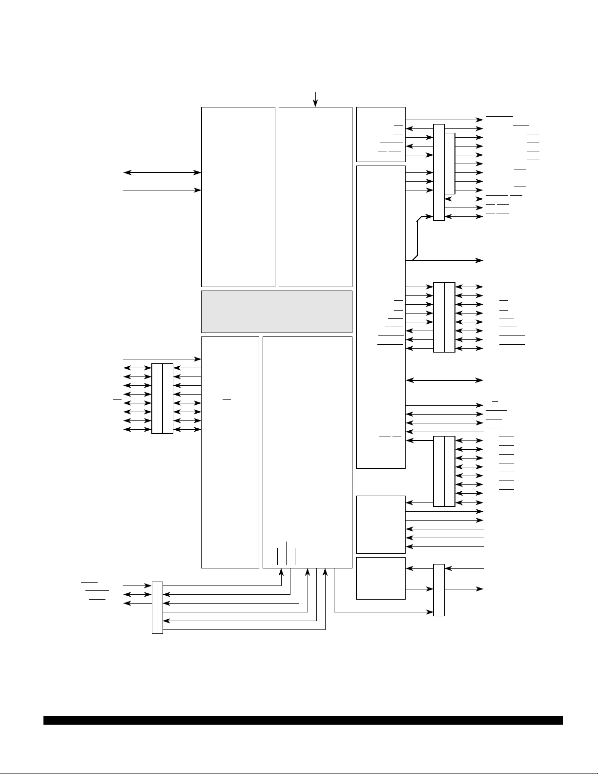
1.2 Block Diagram
V
STBY
TPUCH[15:0] TPUCH[15:0]
T2CLK T2CLK
RXD
PQS7/TXD
PQS6/PCS3
QS5/PCS2
PQS4/PCS1
PQS3/PCS0/SS PCS0/SS
PQS2/SCK
PQS1/MOSI
PQS0/MISO
BKPT/DSCLK
IFETCH
/DSI
IPIPE/DSO
PORT QS
CONTROL
TXD
PCS3
PCS2
PCS1
SCK
MOSI
MISO
QSM
TPU
IMB
BKPT
2 KBYTES
RAM
CPU 32
IPIPE
IFETCH
DSI
DSO
FREEZE
DSCLK
CHIP
SELECTS
BR
BG
BGACK
[10:0]
CS
FC2
FC1
FC0
ADDR[23:0]
SIZ1 PE7/SIZ1
SIZ0 PE6/SIZ0
EBI
DS PE5/DS
AS
RMC
AVEC PE2/AVEC
DSACK1 PE1/DSACK1
DSACK0 PE0/DSACK0
IRQ[7:1]
MODCLK
CLOCK
TSC
TEST
QUOT
CONTROL
ADDR[23:19]
CONTROL
CONTROL
CONTROL
PORT E
PORT F PORT C
CSBOOT
ADDR23/CS10
PC6/ADDR22/CS9
PC5/ADDR21/CS8
PC4/ADDR20/CS7
PC3/ADDR19/CS6
PC2/FC2/CS5
PC1/FC1/CS4
PC0/FC0/CS3
BGACK/CS2
BG/CS1
BR/CS0
ADDR[18:0]
PE4/AS
PE3/RMC
DATA[15:0]DATA[15:0]
R/W
RESET
HALT
BERR
PF7/IRQ7
PF6/IRQ6
PF5/IRQ5
PF4/IRQ4
PF3/IRQ3
PF2/IRQ2
PF1/IRQ1
PF0/MODCLK
CLKOUT
XTAL
EXTAL
XFC
V
TSC
FREEZE/QUOT
DDSYN
CONTROL
332 BLOCK
Figure 1 MCU Block Diagram
MOTOROLA MC68332
6 MC68332TS/D

1.3 Pin Assignments
V
DD
V
STBY
ADDR1
ADDR2
ADDR3
ADDR4
ADDR5
ADDR6
ADDR7
ADDR8
V
DD
V
SS
ADDR9
ADDR10
ADDR11
ADDR12
V
SS
ADDR13
ADDR14
ADDR15
ADDR16
V
DD
V
SS
ADDR17
ADDR18
PQS0/MISO
PQS1/MOSI
PQS2/SCK
PQS3/PCS0/SS
PQS4/PCS1
PQS5/PCS2
PQS6/PCS3
V
DD
SS
V
TPUCH0
TPUCH1
TPUCH2
TPUCH3
TPUCH4
TPUCH5
TPUCH6
17
16151413121110
18
19
20
21
22
23
24
25
26
27
28
29
30
31
32
33
34
35
36
37
38
39
40
41
42
43
44
45
46
47
48
49
50
51
52535455565758596061626364656667686970717273747576777879808182
DD
VSSV
TPUCH7
9876543
TPUCH8
TPUCH9
TPUCH10
DD
VSSV
TPUCH11
2
1
MC68332
TPUCH13
TPUCH14
TPUCH12
131
130
132
V
TPUCH15
T2CLK
129
128
127
SS
V
DD
126
PC6/ADDR22/CS9
ADDR23/CS10
125
124
PC1/FC1/CS4
PC2/FC2/CS5
PC3/ADDR19/CS6
PC4/ADDR20/CS7
PC5/ADDR21/CS8
123
122
121
120
119
SS
PC0/FC0/CS3
V
117
118
116
115
114
113
112
111
110
109
108
107
106
105
104
103
102
101
100
99
98
97
96
95
94
93
92
91
90
89
88
87
86
85
84
83
V
DD
BGACK/CS2
BG/CS1
BR/CS0
CSBOOT
DATA0
DATA1
DATA2
DATA3
V
DD
V
SS
DATA4
DATA5
DATA6
DATA7
V
SS
DATA8
DATA9
DATA10
DATA11
V
DD
V
SS
DATA12
DATA13
DATA14
DATA15
ADDR0
PE0/DSACK0
PE1/DSACK1
PE2/AVEC
PE3/RMC
PE5/DS
V
DD
PE7/SIZ1
PE6/SIZ0
AS
SS
V
332 132-PIN QFP
SS
V
PQS7/TXD
RXD
IPIPE/DSO
IFETCH/DSI
TSC
BKPT/DSCLK
SS
V
XTAL
DDSYN
V
FREEZE/QUOT
XFC
VDDVDDV
EXTAL
SS
CLKOUT
HALT
RESET
BERR
PF7/IRQ7
PF5/IRQ5
PF6/IRQ6
PF2/IRQ2
PF3/IRQ3
PF4/IRQ4
R/W
PF1/IRQ1
PF0/MODCLK
Figure 2 MC68332 132-Pin QFP Pin Assignments
MC68332 MOTOROLA
MC68332TS/D 7

NC
V
SS
FC0/CS3
FC1/CS4
FC2/CS5
ADDR19/CS6
ADDR20/CS7
ADDR21/CS8
ADDR22/CS9
ADDR23/CS10
V
DD
V
SS
T2CLK
TPUCH15
TPUCH14
TPUCH13
TPUCH12
NC
V
DD
V
SS
TPUCH11
TPUCH10
TPUCH9
TPUCH8
V
DDE
V
SSE
TPUCH7
TPUCH6
TPUCH5
TPUCH4
TPUCH3
TPUCH2
TPUCH1
TPUCH0
V
SS
NC
DD
BGACK/CS2
BG/CS1
BR/CS0
CSBOOT
142
141
140
DATA0
139
V
143
144
1
2
3
4
5
6
7
8
9
10
11
12
13
14
15
16
17
18
19
20
21
22
23
24
25
26
27
28
29
30
31
32
33
34
35
36
37
383940414243444546474849505152535455565758596061626364666769707172
DATA1
DATA2
138
137
DD
DATA3
136
135
VSSV
134
DATA4
DATA5
133
132
SS
DATA6
DATA7NCDATA8NCDATA9
V
131
130
129
128
127
126
MC68332
125
DD
DATA10NCDATA11
124
123
122
V
121
VSSDATA12
120
119
DATA13
DATA14
118
117
DATA15
ADDR0
116
115
65
PE0/DSACK0
PE1/DSACK1
PE2/AVEC
PE3/RMC
114
113
112
111
68
DD
PE5/DS
V
109
110
108
107
106
105
104
103
102
101
100
99
98
97
96
95
94
93
92
91
90
89
88
87
86
85
84
83
82
81
80
79
78
77
76
75
74
73
NC
V
SS
PE4/AS
PE6/SIZ0
PE7/SIZ1
R/W
PF0/MODCLK
PF1/IRQ1
PF2/IRQ2
PF3/IRQ3
PF4/IRQ4
PF5/IRQ5
PF6/IRQ6
PF7/IRQ7
BERR
HALT
RESET
V
SS
CLKOUT
V
DD
NC
XFC
V
DD
EXTAL
V
DD
XTAL
V
SS
FREEZE/QUOT
TSC
BKPT/DSCLK
IFETCH/DSI
IPIPE/DSO
RXD
PQS7/TXD
V
SS
NC
SS
ADDR6
ADDR7
DD
V
ADDR8
V
ADDR9
ADDR10
DD
V
STBY
V
ADDR1
ADDR2
ADDR3
ADDR4
ADDR5
NC
ADDR11
ADDR12
SS
NC
V
ADDR13
ADDR14
ADDR15NCADDR16
SS
DD
V
V
ADDR17
ADDR18
PQS2/SCK
PQS0/MISO
PQS1/MOSI
PQS3/PCS0/SS
DD
V
PQS4/PCS1
PQS5/PCS2
PQS6/PCS3
332 144-PIN QFP
Figure 3 MC68332 144-Pin QFP Pin Assignments
MOTOROLA MC68332
8 MC68332TS/D
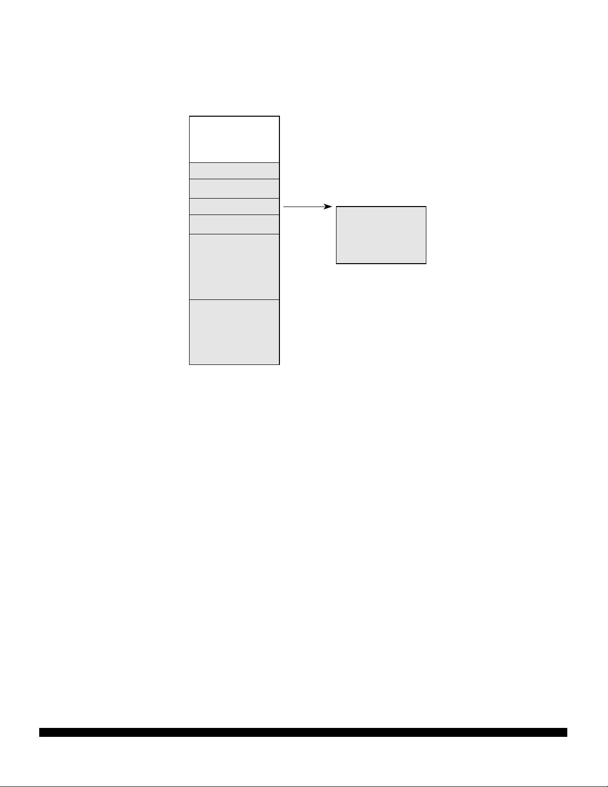
1.4 Address Map
The following figure is a map of the MCU internal addresses. The RAM array is positioned by the base
address registers in the associated RAM control block. Unimplemented blocks are mapped externally.
$YFF000
$YFFA00
$YFFA80
$YFFB00
$YFFB40
$YFFC00
$YFFE00
$YFFFFF
SIM
RESERVED
TPURAM CONTROL
RESERVED
QSM
TPU
2-KBYTE
TPURAM ARRAY
332 ADDRESS MAP
Figure 4 MCU Address Map
1.5 Intermodule Bus
The intermodule bus (IMB) is a standardized bus developed to facilitate both design and operation of
modular microcontrollers. It contains circuitry to support exception processing, address space partitioning, multiple interrupt levels, and vectored interrupts. The standardized modules in the MCU communicate with one another and with external components through the IMB. The IMB in the MCU uses 24
address and 16 data lines.
MC68332 MOTOROLA
MC68332TS/D 9

2 Signal Descriptions
2.1 Pin Characteristics
The following table shows MCU pins and their characteristics. All inputs detect CMOS logic levels. All
inputs can be put in a high-impedance state, but the method of doing this differs depending upon pin
function. Refer to the table, MCU Driver Types, for a description of output drivers. An entry in the discrete I/O column of the MCU Pin Characteristics table indicates that a pin has an alternate I/O function.
The port designation is given when it applies. Refer to the MCU Block Diagram for information about
port organization.
Table 2 MCU Pin Characteristic
Pin
Mnemonic
ADDR23/CS10
ADDR[22:19]/CS[9:6]
ADDR[18:0] A Y N — —
BG
BGACK
BKPT
BR
CLKOUT A — — — —
CSBOOT
DATA[15:0]
DSACK1
DSACK0
DSI/IFETCH
DSO/IPIPE
EXTAL
FC[2:0]/CS[5:3]
FREEZE/QUOT A — — — —
IRQ[7:1]
MODCLK
PCS0/SS Bo Y Y I/O PQS3
PCS[3:1] Bo Y Y I/O PQS[6:4]
RESET
SIZ[1:0] B Y N I/O PE[7:6]
/ECLK A Y N O —
AS
AVEC
BERR
/CS1 B — — — —
/CS2 B Y N — —
/DSCLK — Y Y — —
/CS0 BY N ——
1
DS
2
HALT
B Y Y I/O PF[7:1]
MISO Bo Y Y I/O PQS0
1
MOSI Bo Y Y I/O PQS1
R/W
RMC
RXD — N N — —
SCK Bo Y Y I/O PQS2
Output
Driver
A Y N O PC[6:3]
B Y N I/O PE5
B Y N I/O PE2
BY N — —
B — — — —
Aw Y N — —
B Y N I/O PE4
B Y N I/O PE1
B Y N I/O PE0
AY Y ——
A— — ——
— — Special — —
A Y N O PC[2:0]
Bo Y N — —
B Y N I/O PF0
AY N — —
Bo Y Y — —
B Y N I/O PE3
Input
Synchronized
Input
Hysteresis
Discrete
I/O
Designation
Port
MOTOROLA MC68332
10 MC68332TS/D
Table 2 MCU Pin Characteristic (Continued)
Pin
Mnemonic
Output
Driver
Input
Synchronized
Input
Hysteresis
Discrete
I/O
T2CLK — Y Y — —
TPUCH[15:0] A Y Y — —
TSC — Y Y — —
TXD Bo Y Y I/O PQS7
XFC
XTAL
2
2
— — — Special —
— — — Special —
NOTES:
1. DATA[15:0] are synchronized during reset only. MODCLK is synchronized only when used as an input port pin.
2. EXTAL, XFC, and XTAL are clock reference connections.
2.2 MCU Power Connections
Table 3 MCU Power Connections
V
V
V
STBY
V
DDSYN
SSE
SSI
/V
/V
DDE
DDI
Standby RAM Power/Clock Synthesizer Power
Clock Synthesizer Power
External Periphery Power (Source and Drain)
Internal Module Power (Source and Drain)
Port
Designation
2.3 MCU Driver Types
Type I/O Description
A O Output-only signals that are always driven; no external pull-up required
Aw O Type A output with weak P-channel pull-up during reset
B O Three-state output that includes circuitry to pull up output before high impedance is
Bo O Type B output that can be operated in an open-drain mode
Table 4 MCU Driver Types
established, to ensure rapid rise time. An external holding resistor is required to maintain
logic level while the pin is in the high-impedance state.
MC68332 MOTOROLA
MC68332TS/D 11

2.4 Signal Characteristics
Signal Name MCU Module Signal Type Active State
ADDR[23:0] SIM Bus —
AS SIM Output 0
AVEC
BERR
BG
BGACK
BKPT
BR
CLKOUT SIM Output —
CS[10:0]
CSBOOT
DATA[15:0] SIM Bus —
DS
DSACK[1:0]
DSCLK CPU32 Input Serial Clock
DSI CPU32 Input (Serial Data)
DSO CPU32 Output (Serial Data)
EXTAL SIM Input —
FC[2:0] SIM Output —
FREEZE SIM Output 1
HALT
IFETCH
IPIPE
IRQ[7:1]
MISO QSM Input/Output —
MODCLK SIM Input —
MOSI QSM Input/Output —
PC[6:0] SIM Output (Port)
PCS[3:0] QSM Input/Output —
PE[7:0] SIM Input/Output (Port)
PF[7:0] SIM Input/Output (Port)
PQS[7:0] QSM Input/Output (Port)
QUOT SIM Output —
RESET
RMC
R/W
RXD QSM Input —
SCK QSM Input/Output —
SIZ[1:0] SIM Output —
SS
T2CLK TPU Input —
TPUCH[15:0] TPU Input/Output 1
Table 5 MCU Signal Characteristics
SIM Input 0
SIM Input 0
SIM Output 0
SIM Input 0
CPU32 Input 0
SIM Input 0
SIM Output 0
SIM Output 0
SIM Output 0
SIM Input 0
SIM Input/Output 0
CPU32 Output —
CPU32 Output —
SIM Input 0
SIM Input/Output 0
SIM Output 0
SIM Output 1/0
QSM Input 0
MOTOROLA MC68332
12 MC68332TS/D

Table 5 MCU Signal Characteristics (Continued)
Signal Name MCU Module Signal Type Active State
TSC SIM Input —
TXD QSM Output —
XFC SIM Input —
XTAL SIM Output —
2.5 Signal Function
Table 6 MCU Signal Function
Signal Name Mnemonic Function
Address Bus ADDR[23:0] 24-bit address bus
Address Strobe AS
Autovector AVEC
Bus Error BERR
Bus Grant BG
Bus Grant Acknowledge BGACK
Breakpoint BKPT
Bus Request BR
System Clockout CLKOUT System clock output
Chip Selects CS[10:0]
Boot Chip Select CSBOOT
Data Bus DATA[15:0] 16-bit data bus
Data Strobe DS
Data and Size Acknowledge DSACK[1:0]
Development Serial In, Out,
Clock
Crystal Oscillator EXTAL, XTAL Connections for clock synthesizer circuit reference;
Function Codes FC[2:0] Identify processor state and current address space
Freeze FREEZE Indicates that the CPU has entered background mode
Halt HALT
Instruction Pipeline IFETCH
Interrupt Request Level IRQ[7:1]
Master In Slave Out MISO Serial input to QSPI in master mode;
Clock Mode Select MODCLK Selects the source and type of system clock
Master Out Slave In MOSI Serial output from QSPI in master mode;
Port C PC[6:0] SIM digital output port signals
Peripheral Chip Select PCS[3:0] QSPI peripheral chip selects
Port E PE[7:0] SIM digital I/O port signals
Port F PF[7:0] SIM digital I/O port signals
Port QS PQS[7:0] QSM digital I/O port signals
DSI, DSO,
DSCLK
IPIPE
Indicates that a valid address is on the address bus
Requests an automatic vector during interrupt acknowledge
Indicates that a bus error has occurred
Indicates that the MCU has relinquished the bus
Indicates that an external device has assumed bus mastership
Signals a hardware breakpoint to the CPU
Indicates that an external device requires bus mastership
Select external devices at programmed addresses
Chip select for external boot start-up ROM
During a read cycle, indicates when it is possible for an external
device to place data on the data bus. During a write cycle, indicates that valid data is on the data bus.
Provide asynchronous data transfers and dynamic bus sizing
Serial I/O and clock for background debugging mode
a crystal or an external oscillator can be used
Suspend external bus activity
Indicate instruction pipeline activity
Provides an interrupt priority level to the CPU
serial output from QSPI in slave mode
serial input to QSPI in slave mode
MC68332 MOTOROLA
MC68332TS/D 13

Table 6 MCU Signal Function (Continued)
Signal Name Mnemonic Function
Quotient Out QUOT Provides the quotient bit of the polynomial divider
Reset RESET System reset
Read-Modify-Write Cycle RMC
Read/Write R/W
SCI Receive Data RXD Serial input to the SCI
QSPI Serial Clock SCK Clock output from QSPI in master mode;
Size SIZ[1:0] Indicates the number of bytes to be transferred during a bus cycle
Slave Select SS
TCR2 Clock T2CLK External clock source for TCR2 counter
TPU Channel Pins TPUCH[15:0] Bidirectional pins associated with TPU channels
Three-State Control TSC Places all output drivers in a high-impedance state
SCI Transmit Data TXD Serial output from the SCI
External Filter Capacitor XFC Connection for external phase-locked loop filter capacitor
Indicates an indivisible read-modify-write instruction
Indicates the direction of data transfer on the bus
clock input to QSPI in slave mode
Causes serial transmission when QSPI is in slave mode;
causes mode fault in master mode
MOTOROLA MC68332
14 MC68332TS/D
3 System Integration Module
The MCU system integration module (SIM) consists of five functional blocks that control system startup, initialization, configuration, and external bus.
SYSTEM CONFIGURATION
AND PROTECTION
CLKOUT
CLOCK SYNTHESIZER
EXTAL
MODCLK
CHIP SELECTS
EXTERNAL BUS INTERFACE
FACTORY TEST
CHIP SELECTS
EXTERNAL BUS
RESET
TSC
FREEZE/QUOT
S(C)IM BLOCK
Figure 5 SIM Block Diagram
3.1 Overview
The system configuration and protection block controls MCU configuration and operating mode. The
block also provides bus and software watchdog monitors.
The system clock generates clock signals used by the SIM, other IMB modules, and external devices.
In addition, a periodic interrupt generator supports execution of time-critical control routines.
The external bus interface handles the transfer of information between IMB modules and external address space.
The chip-select block provides eleven general-purpose chip-select signals and a boot ROM chip select
signal. Both general-purpose and boot ROM chip-select signals have associated base address registers and option registers.
The system test block incorporates hardware necessary for testing the MCU. It is used to perform factory tests, and its use in normal applications is not supported.
The SIM control register address map occupies 128 bytes. Unused registers within the 128-byte address space return zeros when read. The “Access” column in the SIM address map below indicates
which registers are accessible only at the supervisor privilege level and which can be assigned to either
the supervisor or user privilege level, according to the value of the SUPV bit in the SIMCR.
MC68332 MOTOROLA
MC68332TS/D 15

Table 7 SIM Address Map
Access Address 15 8 7 0
S $YFFA00 SIM CONFIGURATION (SIMCR)
S $YFFA02 FACTORY TEST (SIMTR)
S $YFFA04 CLOCK SYNTHESIZER CONTROL (SYNCR)
S $YFFA06 NOT USED RESET STATUS REGISTER (RSR)
S $YFFA08 MODULE TEST E (SIMTRE)
S $YFFA0A NOT USED NOT USED
S $YFFA0C NOT USED NOT USED
S $YFFA0E NOT USED NOT USED
S/U $YFFA10 NOT USED PORT E DATA (PORTE0)
S/U $YFFA12 NOT USED PORT E DATA (PORTE1)
S/U $YFFA14 NOT USED PORT E DATA DIRECTION (DDRE)
S $YFFA16 NOT USED PORT E PIN ASSIGNMENT (PEPAR)
S/U $YFFA18 NOT USED PORT F DATA (PORTF0)
S/U $YFFA1A NOT USED PORT F DATA (PORTF1)
S/U $YFFA1C NOT USED PORT F DATA DIRECTION (DDRF)
S $YFFA1E NOT USED PORT F PIN ASSIGNMENT (PFPAR)
S $YFFA20 NOT USED SYSTEM PROTECTION CONTROL
(SYPCR)
S $YFFA22 PERIODIC INTERRUPT CONTROL (PICR)
S $YFFA24 PERIODIC INTERRUPT TIMING (PITR)
S $YFFA26 NOT USED SOFTWARE SERVICE (SWSR)
S $YFFA28 NOT USED NOT USED
S $YFFA2A NOT USED NOT USED
S $YFFA2C NOT USED NOT USED
S $YFFA2E NOT USED NOT USED
S $YFFA30 TEST MODULE MASTER SHIFT A (TSTMSRA)
S $YFFA32 TEST MODULE MASTER SHIFT B (TSTMSRB)
S $YFFA34 TEST MODULE SHIFT COUNT (TSTSC)
S $YFFA36 TEST MODULE REPETITION COUNTER (TSTRC)
S $YFFA38 TEST MODULE CONTROL (CREG)
S/U $YFFA3A TEST MODULE DISTRIBUTED REGISTER (DREG)
$YFFA3C NOT USED NOT USED
$YFFA3E NOT USED NOT USED
S/U $YFFA40 NOT USED PORT C DATA (PORTC)
$YFFA42 NOT USED NOT USED
S $YFFA44 CHIP-SELECT PIN ASSIGNMENT (CSPAR0)
S $YFFA46 CHIP-SELECT PIN ASSIGNMENT (CSPAR1)
S $YFFA48 CHIP-SELECT BASE BOOT (CSBARBT)
S $YFFA4A CHIP-SELECT OPTION BOOT (CSORBT)
S $YFFA4C CHIP-SELECT BASE 0 (CSBAR0)
S $YFFA4E CHIP-SELECT OPTION 0 (CSOR0)
S $YFFA50 CHIP-SELECT BASE 1 (CSBAR1)
S $YFFA52 CHIP-SELECT OPTION 1 (CSOR1)
S $YFFA54 CHIP-SELECT BASE 2 (CSBAR2)
MOTOROLA MC68332
16 MC68332TS/D

Table 7 SIM Address Map (Continued)
Access Address 15 8 7 0
S $YFFA56 CHIP-SELECT OPTION 2 (CSOR2)
S $YFFA58 CHIP-SELECT BASE 3 (CSBAR3)
S $YFFA5A CHIP-SELECT OPTION 3 (CSOR3)
S $YFFA5C CHIP-SELECT BASE 4 (CSBAR4)
S $YFFA5E CHIP-SELECT OPTION 4 (CSOR4)
S $YFFA60 CHIP-SELECT BASE 5 (CSBAR5)
S $YFFA62 CHIP-SELECT OPTION 5 (CSOR5)
S $YFFA64 CHIP-SELECT BASE 6 (CSBAR6)
S $YFFA66 CHIP-SELECT OPTION 6 (CSOR6)
S $YFFA68 CHIP-SELECT BASE 7 (CSBAR7)
S $YFFA6A CHIP-SELECT OPTION 7 (CSOR7)
S $YFFA6C CHIP-SELECT BASE 8 (CSBAR8)
S $YFFA6E CHIP-SELECT OPTION 8 (CSOR8)
S $YFFA70 CHIP-SELECT BASE 9 (CSBAR9)
S $YFFA72 CHIP-SELECT OPTION 9 (CSOR9)
S $YFFA74 CHIP-SELECT BASE 10 (CSBAR10)
S $YFFA76 CHIP-SELECT OPTION 10 (CSOR10)
$YFFA78 NOT USED NOT USED
$YFFA7A NOT USED NOT USED
$YFFA7C NOT USED NOT USED
$YFFA7E NOT USED NOT USED
Y = M111, where M is the logic state of the module mapping (MM) bit in the SIMCR.
3.2 System Configuration and Protection
This functional block provides configuration control for the entire MCU. It also performs interrupt arbitration, bus monitoring, and system test functions. MCU system protection includes a bus monitor, a
HALT monitor, a spurious interrupt monitor, and a software watchdog timer. These functions have been
made integral to the microcontroller to reduce the number of external components in a complete control
system.
MC68332 MOTOROLA
MC68332TS/D 17
MODULE CONFIGURATION
AND TEST
RESET STATUS
CLOCK
9
2
PRESCALER
HALT MONITOR
BUS MONITOR
SPURIOUS INTERRUPT MONITOR
SOFTWARE WATCHDOG TIMER
PERIODIC INTERRUPT TIMER
RESET REQUEST
BERR
RESET
REQUEST
IRQ [7:1]
SYS PROTECT BLOCK
Figure 6 System Configuration and Protection Block
3.2.1 System Configuration
The SIM controls MCU configuration during normal operation and during internal testing.
SIMCR —SIM Configuration Register
15
EXOFF FRZSW FRZBM 0 SLVEN 0 SHEN SUPV MM 0 0 IARB
RESET:
0 0 0 0 DATA11 0 0 0 1 1 0 0 1 1 1 1
14 13 12 11 10 9 8 7 6 5 4 3 0
$YFFA00
The SIM configuration register controls system configuration. It can be read or written at any time, except for the module mapping (MM) bit, which can be written only once.
MOTOROLA MC68332
18 MC68332TS/D

EXOFF — External Clock Off
0 = The CLKOUT pin is driven from an internal clock source.
1 = The CLKOUT pin is placed in a high-impedance state.
FRZSW — Freeze Software Enable
0 = When FREEZE is asserted, the software watchdog and periodic interrupt timer counters con-
tinue to run.
1 = When FREEZE is asserted, the software watchdog and periodic interrupt timer counters are dis-
abled, preventing interrupts during software debug.
FRZBM — Freeze Bus Monitor Enable
0 = When FREEZE is asserted, the bus monitor continues to operate.
1 = When FREEZE is asserted, the bus monitor is disabled.
SLVEN — Factory Test Mode Enabled
This bit is a read-only status bit that reflects the state of DATA11 during reset.
0 = IMB is not available to an external master.
1 = An external bus master has direct access to the IMB.
SHEN[1:0] — Show Cycle Enable
This field determines what the EBI does with the external bus during internal transfer operations. A
show cycle allows internal transfers to be externally monitored. The table below shows whether show
cycle data is driven externally, and whether external bus arbitration can occur. To prevent bus conflict,
external peripherals must not be enabled during show cycles.
SHEN Action
00 Show cycles disabled, external arbitration enabled
01 Show cycles enabled, external arbitration disabled
10 Show cycles enabled, external arbitration enabled
11 Show cycles enabled, external arbitration enabled,
internal activity is halted by a bus grant
SUPV — Supervisor/Unrestricted Data Space
The SUPV bit places the SIM global registers in either supervisor or user data space.
0 = Registers with access controlled by the SUPV bit are accessible from either the user or super-
visor privilege level.
1 = Registers with access controlled by the SUPV bit are restricted to supervisor access only.
MM — Module Mapping
0 = Internal modules are addressed from $7FF000 –$7FFFFF.
1 = Internal modules are addressed from $FFF000 –$FFFFFF.
IARB[3:0] — Interrupt Arbitration Field
Each module that can generate interrupt requests has an interrupt arbitration (IARB) field. Arbitration
between interrupt requests of the same priority is performed by serial contention between IARB field bit
values. Contention must take place whenever an interrupt request is acknowledged, even when there
is only a single pending request. An IARB field must have a non-zero value for contention to take place.
If an interrupt request from a module with an IARB field value of %0000 is recognized, the CPU processes a spurious interrupt exception. Because the SIM routes external interrupt requests to the CPU,
the SIM IARB field value is used for arbitration between internal and external interrupts of the same priority. The reset value of IARB for the SIM is %1111, and the reset IARB value for all other modules is
%0000, which prevents SIM interrupts from being discarded during initialization.
MC68332 MOTOROLA
MC68332TS/D 19

3.2.2 System Protection Control Register
The system protection control register controls system monitor functions, software watchdog clock
prescaling, and bus monitor timing. This register can be written only once following power-on or reset,
but can be read at any time.
SYPCR —System Protection Control Register
15
NOT USED SWE SWP SWT HME BME BMT
RESET:
8 7 6 5 4 3 2 1 0
1 MODCLK 0 0 0 0 0 0
SWE — Software Watchdog Enable
0 = Software watchdog disabled
1 = Software watchdog enabled
SWP — Software Watchdog Prescale
This bit controls the value of the software watchdog prescaler.
0 = Software watchdog clock not prescaled
1 = Software watchdog clock prescaled by 512
SWT[1:0] — Software Watchdog Timing
This field selects the divide ratio used to establish software watchdog time-out period. The following table gives the ratio for each combination of SWP and SWT bits.
SWP SWT Ratio
000
001
010
011
100
101
110
111
9
2
11
2
13
2
15
2
18
2
20
2
22
2
24
2
$YFFA21
HME — Halt Monitor Enable
0 = Disable halt monitor function
1 = Enable halt monitor function
BME — Bus Monitor External Enable
0 = Disable bus monitor function for an internal to external bus cycle.
1 = Enable bus monitor function for an internal to external bus cycle.
BMT[1:0] — Bus Monitor Timing
This field selects a bus monitor time-out period as shown in the following table.
BMT Bus Monitor Time-out Period
00 64 System Clocks
01 32 System Clocks
10 16 System Clocks
11 8 System Clocks
MOTOROLA MC68332
20 MC68332TS/D

3.2.3 Bus Monitor
The internal bus monitor checks for excessively long DSACK
response times during normal bus cycles
and for excessively long DSACK or AVEC response times during interrupt acknowledge cycles. The
monitor asserts BERR if response time is excessive.
DSACK and AVEC response times are measured in clock cycles. The maximum allowable response
time can be selected by setting the BMT field.
The monitor does not check DSACK response on the external bus unless the CPU initiates the bus cycle. The BME bit in the SYPCR enables the internal bus monitor for internal to external bus cycles. If a
system contains external bus masters, an external bus monitor must be implemented and the internal
to external bus monitor option must be disabled.
3.2.4 Halt Monitor
The halt monitor responds to an assertion of HALT
on the internal bus. A flag in the reset status register
(RSR) indicates that the last reset was caused by the halt monitor. The halt monitor reset can be inhibited by the HME bit in the SYPCR.
3.2.5 Spurious Interrupt Monitor
The spurious interrupt monitor issues BERR if no interrupt arbitration occurs during an interrupt-acknowledge cycle.
3.2.6 Software Watchdog
The software watchdog is controlled by SWE in the SYPCR. Once enabled, the watchdog requires that
a service sequence be written to SWSR on a periodic basis. If servicing does not take place, the watchdog times out and issues a reset. This register can be written at any time, but returns zeros when read.
SWSR —Software Service Register $YFFA27
15 8 7 6 5 4 3 2 1 0
NOT USED 0 0 0 0 0 0 0 0
RESET:
0 0 0 0 0 0 0 0
Register shown with read value
Perform a software watchdog service sequence as follows:
a. Write $55 to SWSR.
b. Write $AA to SWSR.
Both writes must occur before time-out in the order listed, but any number of instructions can be executed between the two writes.
The watchdog clock rate is affected by SWP and SWT in SYPCR. When SWT[1:0] are modified, a
watchdog service sequence must be performed before the new time-out period takes effect.
The reset value of SWP is affected by the state of the MODCLK pin on the rising edge of reset, as shown
in the following table.
MODCLK SWP
01
10
MC68332 MOTOROLA
MC68332TS/D 21

3.2.7 Periodic Interrupt Timer
The periodic interrupt timer (PIT) generates interrupts of specified priorities at specified intervals. Timing
for the PIT is provided by a programmable prescaler driven by the system clock.
PICR — Periodic Interrupt Control Register $YFFA22
15 14 13 12 11 10 8 7 0
0 0 0 0 0 PIRQL PIV
RESET:
0 0 0 0 0 0 0 0 0 0 0 0 1 1 1 1
This register contains information concerning periodic interrupt priority and vectoring. Bits [10:0] can be
read or written at any time. Bits [15:11] are unimplemented and always return zero.
PIRQL[2:0] — Periodic Interrupt Request Level
The following table shows what interrupt request level is asserted when a periodic interrupt is generated. If a PIT interrupt and an external IRQ
signal of the same priority occur simultaneously, the PIT in-
terrupt is serviced first. The periodic timer continues to run when the interrupt is disabled.
PIRQL Interrupt Request Level
000 Periodic Interrupt Disabled
001 Interrupt Request Level 1
010 Interrupt Request Level 2
011 Interrupt Request Level 3
100 Interrupt Request Level 4
101 Interrupt Request Level 5
110 Interrupt Request Level 6
111 Interrupt Request Level 7
PIV[7:0] — Periodic Interrupt Vector
The bits of this field contain the vector generated in response to an interrupt from the periodic timer.
When the SIM responds, the periodic interrupt vector is placed on the bus.
PITR —Periodic Interrupt Timer Register $YFFA24
15 14 13 12 11 10 9 8 7 0
0 0 0 0 0 0 0 PTP PITM
RESET:
0 0 0 0 0 0 0 MODCLK 0 0 0 0 0 0 0 0
The PITR contains the count value for the periodic timer. A zero value turns off the periodic timer. This
register can be read or written at any time.
PTP — Periodic Timer Prescaler Control
0 = Periodic timer clock not prescaled
1 = Periodic timer clock prescaled by a value of 512
The reset state of PTP is the complement of the state of the MODCLK signal during reset.
PITM[7:0] — Periodic Interrupt Timing Modulus Field
This is an 8-bit timing modulus. The period of the timer can be calculated as follows:
PIT Period = [(PITM)(Prescaler)(4)]/EXTAL
where
PIT Period = Periodic interrupt timer period
PITM = Periodic interrupt timer register modulus (PITR[7:0])
EXTAL Frequency = Crystal frequency
Prescale = 512 or 1 depending on the state of the PTP bit in the PITR
MOTOROLA MC68332
22 MC68332TS/D
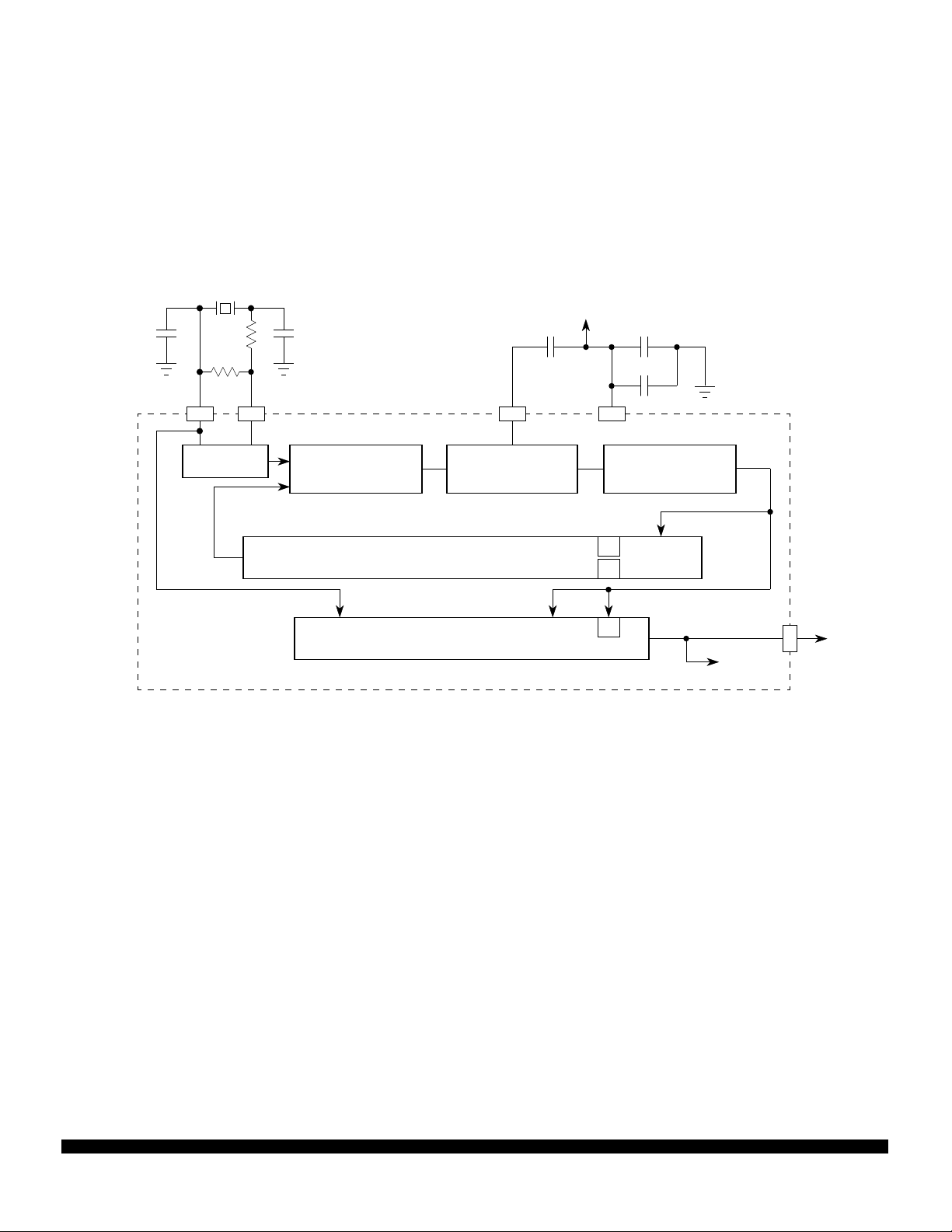
3.3 System Clock
The system clock in the SIM provides timing signals for the IMB modules and for an external peripheral
bus. Because MCU operation is fully static, register and memory contents are not affected when the
clock rate changes. System hardware and software support changes in the clock rate during operation.
The system clock signal can be generated in three ways. An internal phase-locked loop can synthesize
the clock from an internal or external frequency source, or the clock signal can be input from an external
source.
Following is a block diagram of the clock submodule.
V
DDSYN
22 pF
V
SSI
2
EXTAL
330k
10M
2
22 pF
V
SSI
XTAL XFC PIN
XFC
0.1µF
V
1
DDSYN
0.1µF
.01µF
V
SSI
CRYSTAL
OSCILLATOR
1. MUST BE LOW-LEAKAGE CAPACITOR (INSULATION RESISTANCE 30,000 MΩ OR GREATER).
2. RESISTANCE AND CAPACITANCE BASED ON A TEST CIRCUIT CONSTRUCTED WITH A DAISHINKU DMX-38 32.768-kHz CRYSTAL.
SPECIFIC COMPONENTS MUST BE BASED ON CRYSTAL TYPE. CONTACT CRYSTAL VENDOR FOR EXACT CIRCUIT.
PHASE
COMPARATOR
LOW-PASS
FILTER
FEEDBACK DIVIDER
SYSTEM CLOCK CONTROL
VCO
W
Y
X
SYSTEM
CLOCK
Figure 7 System Clock Block Diagram
3.3.1 Clock Sources
The state of the clock mode (MODCLK) pin during reset determines the clock source. When MODCLK
is held high during reset, the clock synthesizer generates a clock signal from either a crystal oscillator
or an external reference input. Clock synthesizer control register SYNCR determines operating frequency and various modes of operation. When MODCLK is held low during reset, the clock synthesizer is
disabled, and an external system clock signal must be applied. When the synthesizer is disabled, SYNCR control bits have no effect.
CLKOUT
SYS CLOCK
BLOCK 32KHZ
A reference crystal must be connected between the EXTAL and XTAL pins to use the internal oscillator.
Use of a 32.768-kHz crystal is recommended. These crystals are inexpensive and readily available. If
an external reference signal or an external system clock signal is applied through the EXTAL pin, the
XTAL pin must be left floating. External reference signal frequency must be less than or equal to maximum specified reference frequency. External system clock signal frequency must be less than or equal
to maximum specified system clock frequency.
MC68332 MOTOROLA
MC68332TS/D 23

When an external system clock signal is applied (i.e., the PLL is not used), duty cycle of the input is
critical, especially at near maximum operating frequencies. The relationship between clock signal duty
cycle and clock signal period is expressed:
Minimum external clock period =
minimum external clock high/low time
50% — percentage variation of external clock input duty cycle
3.3.2 Clock Synthesizer Operation
A voltage controlled oscillator (VCO) generates the system clock signal. A portion of the clock signal is
fed back to a divider/counter. The divider controls the frequency of one input to a phase comparator.
The other phase comparator input is a reference signal, either from the internal oscillator or from an
external source. The comparator generates a control signal proportional to the difference in phase between its two inputs. The signal is low-pass filtered and used to correct VCO output frequency.
The synthesizer locks when VCO frequency is identical to reference frequency. Lock time is affected by
the filter time constant and by the amount of difference between the two comparator inputs. Whenever
comparator input changes, the synthesizer must re-lock. Lock status is shown by the SLOCK bit in SYNCR.
The MCU does not come out of reset state until the synthesizer locks. Crystal type, characteristic frequency, and layout of external oscillator circuitry affect lock time.
The low-pass filter requires an external low-leakage capacitor, typically 0.1 µF, connected between the
XFC and V
DDSYN
pins.
V
is used to power the clock circuits. A separate power source increases MCU noise immunity
DDSYN
and can be used to run the clock when the MCU is powered down. Use a quiet power supply as the
V
ternal bypass capacitors as close as possible to the V
source, since PLL stability depends on the VCO, which uses this supply. Place adequate ex-
DDSYN
pin to ensure stable operating frequency.
DDSYN
When the clock synthesizer is used, control register SYNCR determines operating frequency and various modes of operation. SYNCR can be read only when the processor is operating at the supervisor
privilege level.
The SYNCR X bit controls a divide by two prescaler that is not in the synthesizer feedback loop. Setting
X doubles clock speed without changing VCO speed. There is no VCO relock delay. The SYNCR W bit
controls a 3-bit prescaler in the feedback divider. Setting W increases VCO speed by a factor of four.
The SYNCR Y field determines the count modulus for a modulo 64 down counter, causing it to divide
by a value of Y + 1. When either W or Y value changes, there is a VCO relock delay.
Clock frequency is determined by SYNCR bit settings as follows:
F
SYSTEM
= F
REFERENCE
[4(Y + 1)(2
2W + X
)]
In order for the device to perform correctly, the clock frequency selected by the W, X, and Y bits must
be within the limits specified for the MCU.
The VCO frequency is twice the system clock frequency if X = 1 or four times the system clock frequency
if X = 0.
The reset state of SYNCR ($3F00) produces a modulus-64 count.
MOTOROLA MC68332
24 MC68332TS/D

3.3.3 Clock Control
The clock control circuits determine system clock frequency and clock operation under special circumstances, such as following loss of synthesizer reference or during low-power operation. Clock source is
determined by the logic state of the MODCLK pin during reset.
SYNCR —Clock Synthesizer Control Register $YFFA04
15 14 13 8 7 6 5 4 3 2 1 0
W X Y EDIV 0 0 SLIMP SLOCK RSTEN STSIM STEXT
RESET:
0 0 1 1 1 1 1 1 0 0 0 U U 0 0 0
When the on-chip clock synthesizer is used, system clock frequency is controlled by the bits in the upper
byte of SYNCR. Bits in the lower byte show status of or control operation of internal and external clocks.
The SYNCR can be read or written only when the CPU is operating at the supervisor privilege level.
W — Frequency Control (VCO)
This bit controls a prescaler tap in the synthesizer feedback loop. Setting the bit increases the VCO
speed by a factor of four. VCO relock delay is required.
X — Frequency Control Bit (Prescale)
This bit controls a divide by two prescaler that is not in the synthesizer feedback loop. Setting the bit
doubles clock speed without changing the VCO speed. There is no VCO relock delay.
Y[5:0] — Frequency Control (Counter)
The Y field controls the modulus down counter in the synthesizer feedback loop, causing it to divide by
a value of Y + 1. Values range from 0 to 63. VCO relock delay is required.
EDIV — E Clock Divide Rate
0 = ECLK frequency is system clock divided by 8.
1 = ECLK frequency is system clock divided by 16.
ECLK is an external M6800 bus clock available on pin ADDR23. Refer to 3.5 Chip Selects for more
information.
SLIMP — Limp Mode Flag
0 = External crystal is VCO reference.
1 = Loss of crystal reference.
When the on-chip synthesizer is used, loss of reference frequency causes SLIMP to be set. The VCO
continues to run using the base control voltage. Maximum limp frequency is maximum specified system
clock frequency. X-bit state affects limp frequency.
SLOCK — Synthesizer Lock Flag
0 = VCO is enabled, but has not locked.
1 = VCO has locked on the desired frequency (or system clock is external).
The MCU maintains reset state until the synthesizer locks, but SLOCK does not indicate synthesizer
lock status until after the user writes to SYNCR.
RSTEN — Reset Enable
0 = Loss of crystal causes the MCU to operate in limp mode.
1 = Loss of crystal causes system reset.
STSIM — Stop Mode SIM Clock
0 = When LPSTOP is executed, the SIM clock is driven from the crystal oscillator and the VCO is
turned off to conserve power.
1 = When LPSTOP is executed, the SIM clock is driven from the VCO.
STEXT — Stop Mode External Clock
0 = When LPSTOP is executed, the CLKOUT signal is held negated to conserve power.
1 = When LPSTOP is executed, the CLKOUT signal is driven from the SIM clock, as determined by
the state of the STSIM bit.
MC68332 MOTOROLA
MC68332TS/D 25

3.4 External Bus Interface
The external bus interface (EBI) transfers information between the internal MCU bus and external devices. The external bus has 24 address lines and 16 data lines.
The EBI provides dynamic sizing between 8-bit and 16-bit data accesses. It supports byte, word, and
long-word transfers. Ports are accessed through the use of asynchronous cycles controlled by the data
transfer (SIZ1 and SIZ0) and data size acknowledge pins (DSACK1 and DSACK0). Multiple bus cycles
may be required for a transfer to or from an 8-bit port.
Port width is the maximum number of bits accepted or provided during a bus transfer. External devices
must follow the handshake protocol described below. Control signals indicate the beginning of the cycle,
the address space, the size of the transfer, and the type of cycle. The selected device controls the length
of the cycle. Strobe signals, one for the address bus and another for the data bus, indicate the validity
of an address and provide timing information for data. The EBI operates in an asynchronous mode for
any port width.
To add flexibility and minimize the necessity for external logic, MCU chip-select logic can be synchronized with EBI transfers. Chip-select logic can also provide internally-generated bus control signals for
these accesses. Refer to 3.5 Chip Selects for more information.
3.4.1 Bus Control Signals
The CPU initiates a bus cycle by driving the address, size, function code, and read/write outputs. At the
beginning of the cycle, size signals SIZ0 and SIZ1 are driven along with the function code signals. The
size signals indicate the number of bytes remaining to be transferred during an operand cycle. They are
valid while the address strobe (AS
) is asserted. The following table shows SIZ0 and SIZ1 encoding. The
read/write (R/W) signal determines the direction of the transfer during a bus cycle. This signal changes
state, when required, at the beginning of a bus cycle, and is valid while AS is asserted. R/W only changes state when a write cycle is preceded by a read cycle or vice versa. The signal can remain low for two
consecutive write cycles.
Table 8 Size Signal Encoding
SIZ1 SIZ0 Transfer Size
0 1 Byte
1 0 Word
1 1 Three Byte
0 0 Long Word
3.4.2 Function Codes
The CPU32 automatically generates function code signals FC[2:0]. The function codes can be considered address extensions that automatically select one of eight address spaces to which an address applies. These spaces are designated as either user or supervisor, and program or data spaces. Address
space 7 is designated CPU space. CPU space is used for control information not normally associated
with read or write bus cycles. Function codes are valid while AS is asserted.
MOTOROLA MC68332
26 MC68332TS/D

Table 9 CPU32 Address Space Encoding
FC2 FC1 FC0 Address Space
0 0 0 Reserved
0 0 1 User Data Space
0 1 0 User Program Space
0 1 1 Reserved
1 0 0 Reserved
1 0 1 Supervisor Data Space
1 1 0 Supervisor Program Space
1 1 1 CPU Space
3.4.3 Address Bus
Address bus signals ADDR[23:0] define the address of the most significant byte to be transferred during
a bus cycle. The MCU places the address on the bus at the beginning of a bus cycle. The address is
valid while AS is asserted.
3.4.4 Address Strobe
AS is a timing signal that indicates the validity of an address on the address bus and the validity of many
control signals. It is asserted one-half clock after the beginning of a bus cycle.
3.4.5 Data Bus
Data bus signals DATA[15:0] make up a bidirectional, non-multiplexed parallel bus that transfers data
to or from the MCU. A read or write operation can transfer 8 or 16 bits of data in one bus cycle. During
a read cycle, the data is latched by the MCU on the last falling edge of the clock for that bus cycle. For
a write cycle, all 16 bits of the data bus are driven, regardless of the port width or operand size. The
MCU places the data on the data bus one-half clock cycle after AS
is asserted in a write cycle.
3.4.6 Data Strobe
Data strobe (DS) is a timing signal. For a read cycle, the MCU asserts DS to signal an external device
to place data on the bus. DS is asserted at the same time as AS during a read cycle. For a write cycle,
DS signals an external device that data on the bus is valid. The MCU asserts DS one full clock cycle
after the assertion of AS during a write cycle.
3.4.7 Bus Cycle Termination Signals
During bus cycles, external devices assert the data transfer and size acknowledge signals (DSACK1
and DSACK0). During a read cycle, the signals tell the MCU to terminate the bus cycle and to latch data.
During a write cycle, the signals indicate that an external device has successfully stored data and that
the cycle can end. These signals also indicate to the MCU the size of the port for the bus cycle just completed. (Refer to 3.4.9 Dynamic Bus Sizing.)
The bus error (BERR) signal is also a bus cycle termination indicator and can be used in the absence
of DSACK1 and DSACK0 to indicate a bus error condition. It can also be asserted in conjunction with
these signals, provided it meets the appropriate timing requirements. The internal bus monitor can be
used to generate the BERR signal for internal and internal-to-external transfers. When BERR and HALT
are asserted simultaneously, the CPU takes a bus error exception.
Autovector signal (AVEC) can terminate external IRQ pin interrupt acknowledge cycles. AVEC indicates
that the MCU will internally generate a vector number to locate an interrupt handler routine. If it is continuously asserted, autovectors will be generated for all external interrupt requests. AVEC is ignored
during all other bus cycles.
MC68332 MOTOROLA
MC68332TS/D 27

3.4.8 Data Transfer Mechanism
The MCU architecture supports byte, word, and long-word operands, allowing access to 8- and 16-bit
data ports through the use of asynchronous cycles controlled by the data transfer and size acknowledge
inputs (DSACK1 and DSACK0).
3.4.9 Dynamic Bus Sizing
The MCU dynamically interprets the port size of the addressed device during each bus cycle, allowing
operand transfers to or from 8- and 16-bit ports. During an operand transfer cycle, the slave device signals its port size and indicates completion of the bus cycle to the MCU through the use of the DSACK0
and DSACK1 inputs, as shown in the following table.
Table 10 Effect of DSACK
DSACK1 DSACK0 Result
1 1 Insert Wait States in Current Bus Cycle
1 0 Complete Cycle —Data Bus Port Size is 8 Bits
0 1 Complete Cycle —Data Bus Port Size is 16 Bits
0 0 Reserved
Signals
For example, if the MCU is executing an instruction that reads a long-word operand from a 16-bit port,
the MCU latches the 16 bits of valid data and then runs another bus cycle to obtain the other 16 bits.
The operation for an 8-bit port is similar, but requires four read cycles. The addressed device uses the
DSACK0
and DSACK1 signals to indicate the port width. For instance, a 16-bit device always returns
DSACK0 = 1 and DSACK1 = 0 for a 16-bit port, regardless of whether the bus cycle is a byte or word
operation.
Dynamic bus sizing requires that the portion of the data bus used for a transfer to or from a particular
port size be fixed. A 16-bit port must reside on data bus bits [15:0] and an 8-bit port must reside on data
bus bits [15:8]. This minimizes the number of bus cycles needed to transfer data and ensures that the
MCU transfers valid data.
The MCU always attempts to transfer the maximum amount of data on all bus cycles. For a word operation, it is assumed that the port is 16 bits wide when the bus cycle begins. Operand bytes are designated as shown in the following figure. OP0 is the most significant byte of a long-word operand, and
OP3 is the least significant byte. The two bytes of a word-length operand are OP0 (most significant) and
OP1. The single byte of a byte-length operand is OP0.
Operand Byte Order
31 24 23 16 15 8 7 0
Long Word OP0 OP1 OP2 OP3
Three Byte OP0 OP1 OP2
Word OP0 OP1
Byte OP0
Figure 8 Operand Byte Order
3.4.10 Operand Alignment
The data multiplexer establishes the necessary connections for different combinations of address and
data sizes. The multiplexer takes the two bytes of the 16-bit bus and routes them to their required positions. Positioning of bytes is determined by the size and address outputs. SIZ1 and SIZ0 indicate the
remaining number of bytes to be transferred during the current bus cycle. The number of bytes transferred is equal to or less than the size indicated by SIZ1 and SIZ0, depending on port width.
MOTOROLA MC68332
28 MC68332TS/D

ADDR0 also affects the operation of the data multiplexer. During an operand transfer, ADDR[23:1] indicate the word base address of the portion of the operand to be accessed, and ADDR0 indicates the
byte offset from the base.
3.4.11 Misaligned Operands
CPU32 processor architecture uses a basic operand size of 16 bits. An operand is misaligned when it
overlaps a word boundary. This is determined by the value of ADDR0. When ADDR0 = 0 (an even address), the address is on a word and byte boundary. When ADDR0 = 1 (an odd address), the address
is on a byte boundary only. A byte operand is aligned at any address; a word or long-word operand is
misaligned at an odd address. The CPU32 does not support misaligned operand transfers.
The largest amount of data that can be transferred by a single bus cycle is an aligned word. If the MCU
transfers a long-word operand via a 16-bit port, the most significant operand word is transferred on the
first bus cycle and the least significant operand word on a following bus cycle.
3.4.12 Operand Transfer Cases
The following table summarizes how operands are aligned for various types of transfers. OPn entries
are portions of a requested operand that are read or written during a bus cycle and are defined by SIZ1,
SIZ0, and ADDR0 for that bus cycle.
Table 11 Operand Alignment
Transfer Case SIZ1 SIZ0 ADDR0 DSACK1 DSACK0 DATA
[15:8]
Byte to 8-Bit Port (Even/Odd) 0 1 X 1 0 OP0 (OP0)
Byte to 16-Bit Port (Even) 0 1 0 0 X OP0 (OP0)
Byte to 16-Bit Port (Odd) 0 1 1 0 X (OP0) OP0
Word to 8-Bit Port (Aligned) 1 0 0 1 0 OP0 (OP1)
Word to 8-Bit Port (Misaligned)
Word to 16-Bit Port (Aligned) 1 0 0 0 X OP0 OP1
Word to 16-Bit Port (Misaligned)
3 Byte to 8-Bit Port (Aligned)
3 Byte to 8-Bit Port (Misaligned)
3 Byte to 16-Bit Port (Aligned)
3 Byte to 16-Bit Port (Misaligned)
Long Word to 8-Bit Port (Aligned) 0 0 0 1 0 OP0 (OP1)
Long Word to 8-Bit Port (Misaligned)
Long Word to 16-Bit Port (Aligned) 0 0 0 0 X OP0 OP1
Long Word to 16-Bit Port (Misaligned)
NOTES:
1. Operands in parentheses are ignored by the CPU32 during read cycles.
2. Three-byte transfer cases occur only as a result of a long word to byte transfer.
3. The CPU32 does not support misaligned word or long-word transfers.
3
3
2
2, 3
2
2, 3
3
3
1 0 1 1 0 OP0 (OP0)
1 0 1 0 X (OP0) OP0
1 1 0 1 0 OP0 (OP1)
1 1 1 1 0 OP0 (OP0)
1 1 0 0 X OP0 OP1
1 1 1 0 X (OP0) OP0
1 0 1 1 0 OP0 (OP0)
1 0 1 0 X (OP0) OP0
DATA
[7:0]
3.5 Chip Selects
Typical microcontrollers require additional hardware to provide external chip-select signals. Twelve independently programmable chip selects provide fast two-cycle access to external memory or peripherals. Address block sizes of 2 Kbytes to 1 Mbyte can be selected.
MC68332 MOTOROLA
MC68332TS/D 29

Chip-select assertion can be synchronized with bus control signals to provide output enable, read/write
strobes, or interrupt acknowledge signals. Logic can also generate DSACK signals internally. A single
DSACK generator is shared by all circuits. Multiple chip selects assigned to the same address and control must have the same number of wait states.
Chip selects can also be synchronized with the ECLK signal available on ADDR23.
When a memory access occurs, chip-select logic compares address space type, address, type of ac-
cess, transfer size, and interrupt priority (in the case of interrupt acknowledge) to parameters stored in
chip-select registers. If all parameters match, the appropriate chip-select signal is asserted. Select signals are active low. Refer to the following block diagram of a single chip-select circuit.
INTERNAL
SIGNALS
ADDRESS
BUS CONTROL
AVEC
DSACK
GENERATOR
BASE ADDRESS REGISTER
ADDRESS COMPARATOR
OPTION COMPARE
OPTION REGISTER
AVEC
GENERATOR
DSACK
PIN
ASSIGNMENT
REGISTER
TIMING
AND
CONTROL
REGISTER
PIN
PIN
DATA
CHIP SEL BLOCK
Figure 9 Chip-Select Circuit Block Diagram
The following table lists allocation of chip-selects and discrete outputs on the pins of the MCU.
Pin Chip Select Discrete Outputs
CSBOOT
BR
BG
BGACK
FC0 CS3
FC1 CS4
FC2 CS5
ADDR19 CS6
ADDR20 CS7
ADDR21 CS8
ADDR22 CS9
ADDR23 CS10
CSBOOT —
CS0 —
CS1 —
CS2 —
PC0
PC1
PC2
PC3
PC4
PC5
PC6
ECLK
MOTOROLA MC68332
30 MC68332TS/D

3.5.1 Chip-Select Registers
Pin assignment registers CSPAR0 and CSPAR1 determine functions of chip-select pins. These registers also determine port size (8- or 16-bit) for dynamic bus allocation.
A pin data register (PORTC) latches discrete output data.
Blocks of addresses are assigned to each chip-select function. Block sizes of 2 Kbytes to 1 Mbyte can
be selected by writing values to the appropriate base address register (CSBAR). Address blocks for
separate chip-select functions can overlap.
Chip-select option registers (CSORBT and CSOR[10:0]) determine timing of and conditions for assertion of chip-select signals. Eight parameters, including operating mode, access size, synchronization,
and wait state insertion can be specified.
Initialization code often resides in a peripheral memory device controlled by the chip-select circuits. A
set of special chip-select functions and registers (CSORBT, CSBARBT) is provided to support bootstrap
operation.
3.5.2 Pin Assignment Registers
The pin assignment registers (CSPAR0 and CSPAR1) contain pairs of bits that determine the function
of chip-select pins. The pin assignment encodings used in these registers are shown below.
Table 12 Pin Assignment Encodings
Bit Field Description
00 Discrete Output
01 Alternate Function
10 Chip Select (8-Bit Port)
11 Chip Select (16-Bit Port)
CSPAR0 —Chip Select Pin Assignment Register 0 $YFFA44
15 14 13 12 11 10 9 8 7 6 5 4 3 2 1 0
0 0 CSPA0[6] CSPA0[5] CSPA0[4] CSPA0[3] CSPA0[2] CSPA0[1] CSBOOT
RESET:
0 0 DATA2 1 DATA2 1 DATA2 1 DATA1 1 DATA1 1 DATA1 1 1 DATA0
CSPAR0 contains seven 2-bit fields that determine the functions of corresponding chip-select pins.
CSPAR0[15:14] are not used. These bits always read zero; writes have no effect. CSPAR0 bit 1 always
reads one; writes to CSPAR0 bit 1 have no effect.
Table 13 CSPAR0 Pin Assignments
CSPAR0 Field Chip Select Signal Alternate Signal Discrete Output
CSPA0[6] CS5
CSPA0[5] CS4
CSPA0[4] CS3
CSPA0[3] CS2
CSPA0[2] CS1
CSPA0[1] CS0
CSBOOT
CSBOOT ——
FC2 PC2
FC1 PC1
FC0 PC0
BGACK —
BG —
BR —
MC68332 MOTOROLA
MC68332TS/D 31

CSPAR1 —Chip Select Pin Assignment Register 1 $YFFA46
15 14 13 12 11 10 9 8 7 6 5 4 3 2 1 0
0 0 0 0 0 0 CSPA1[4] CSPA1[3] CSPA1[2] CSPA1[1] CSPA1[0]
RESET:
0 0 0 0 0 0 DATA7 1 DATA
[7:6]
1 DATA
[7:5]
1 DATA
[7:4]
1 DATA
[7:3]
1
CSPAR1 contains five 2-bit fields that determine the functions of corresponding chip-select pins.
CSPAR1[15:10] are not used. These bits always read zero; writes have no effect.
Table 14 CSPAR1 Pin Assignments
CSPAR0 Field Chip Select Signal Alternate Signal Discrete Output
CSPA1[4] CS10
CSPA1[3] CS9
CSPA1[2] CS8
CSPA1[1] CS7
CSPA1[0] CS6
ADDR23 ECLK
ADDR22 PC6
ADDR21 PC5
ADDR20 PC4
ADDR19 PC3
At reset, either the alternate function (01) or chip-select function (11) can be encoded. DATA pins are
driven to logic level one by a weak interval pull-up during reset. Encoding is for chip-select function unless a data line is held low during reset. Note that bus loading can overcome the weak pull-up and hold
pins low during reset. The following table shows the hierarchical selection method that determines the
reset functions of pins controlled by CSPAR1.
Table 15 Reset Pin Function of CS[10:6]
Data Bus Pins at Reset Chip-Select/Address Bus Pin Function
/
DATA7 DATA6 DATA5 DATA4 DATA3 CS10
ADDR23
11111CS10 CS9 CS8 CS7 CS6
11110 CS10 CS9 CS8 CS7 ADDR19
111
11
1
0XXXXADDR23 ADDR22 ADDR21 ADDR20 ADDR19
0 X X X CS10 ADDR22 ADDR21 ADDR20 ADDR19
0 X X CS10 CS9 ADDR21 ADDR20 ADDR19
0 X CS10 CS9 CS8 ADDR20 ADDR19
CS9/
ADDR22
CS8/
ADDR21
CS7/
ADDR20
CS6/
ADDR19
A pin programmed as a discrete output drives an external signal to the value specified in the port C
pin data register (PORTC), with the following exceptions:
1. No discrete output function is available on pins BR, BG, or BGACK.
2. ADDR23 provides E-clock output rather than a discrete output signal.
When a pin is programmed for discrete output or alternate function, internal chip-select logic still functions and can be used to generate DSACK or AVEC internally on an address match.
Port size is determined when a pin is assigned as a chip select. When a pin is assigned to an 8-bit port,
the chip select is asserted at all addresses within the block range. If a pin is assigned to a 16-bit port,
the upper/lower byte field of the option register selects the byte with which the chip select is associated.
MOTOROLA MC68332
32 MC68332TS/D
3.5.3 Base Address Registers
A base address is the starting address for the block enabled by a given chip select. Block size determines the extent of the block above the base address. Each chip select has an associated base register
so that an efficient address map can be constructed for each application. If a chip-select base address
register is programmed with the same address as a microcontroller module or memory array, an access
to that address goes to the module or array and the chip-select signal is not asserted.
CSBARBT — Chip-Select Base Address Register Boot ROM $YFFA48
15 14 13 12 11 10 9 8 7 6 5 4 3 2 0
ADDR23ADDR22ADDR21ADDR20ADDR19ADDR18ADDR17ADDR16ADDR15ADDR14ADDR13ADDR12ADDR
11
RESET:
0 0 0 0 0 0 0 0 0 0 0 0 0 1 1 1
BLKSZ
CSBAR[10:0] —Chip-Select Base Address Registers $YFFA4C–$YFFA74
15 14 13 12 11 10 9 8 7 6 5 4 3 2 0
ADDR23ADDR22ADDR21ADDR20ADDR19ADDR18ADDR17ADDR16ADDR15ADDR14ADDR13ADDR12ADDR
RESET:
0
0 0 0 0 0 0 0 0 0 0 0 0 0 0 0
11
BLKSZ
ADDR[23:11] — Base Address Field
This field sets the starting address of a particular address space. The address compare logic uses only
the most significant bits to match an address within a block. The value of the base address must be a
multiple of block size. Base address register diagrams show how base register bits correspond to address lines.
BLKSZ — Block Size Field
This field determines the size of the block that must be enabled by the chip select. The following table
shows bit encoding for the base address registers block size field.
Block Size Field Block Size Address Lines Compared
000 2 K ADDR[23:11]
001 8 K ADDR[23:13]
010 16 K ADDR[23:14]
011 64 K ADDR[23:16]
100 128 K ADDR[23:17]
101 256 K ADDR[23:18]
110 512 K ADDR[23:19]
111 1 M ADDR[23:20]
3.5.4 Option Registers
The option registers contain eight fields that determine timing of and conditions for assertion of chipselect signals. For a chip-select signal to be asserted, all bits in the base address register must match
the corresponding internal upper address lines, and all conditions specified in the option register must
be satisfied. These conditions also apply to providing DSACK
or autovector support.
MC68332 MOTOROLA
MC68332TS/D 33

CSORBT —Chip-Select Option Register Boot ROM $YFFA4A
15 14 13 12 11 10 9 6 5 4 3 1 0
MODE BYTE R/W STRB DSACK SPACE IPL AVEC
RESET:
0 1 1 1 1 0 1 1 0 1 1 1 0 0 0 0
CSOR[10:0] —Chip-Select Option Registers $YFFA4E–$YFFA76
15 14 13 12 11 10 9 6 5 4 3 1 0
MODE BYTE R/W STRB DSACK SPACE IPL AVEC
RESET:
0 0 0 0 0 0 0 0 0 0 0 0 0 0 0 0
CSORBT, the option register for CSBOOT, contains special reset values that support bootstrap operations from peripheral memory devices.
The following bit descriptions apply to both CSORBT and CSOR[10:0] option registers.
MODE — Asynchronous/Synchronous Mode
0 = Asynchronous mode selected (chip-select assertion determined by internal or external bus con-
trol signals)
1 = Synchronous mode selected (chip-select assertion synchronized with ECLK signal)
In asynchronous mode, the chip select is asserted synchronized with AS or DS.
The DSACK field is not used in synchronous mode because a bus cycle is only performed as a synchronous operation. When a match condition occurs on a chip select programmed for synchronous operation, the chip select signals the EBI that an ECLK cycle is pending.
BYTE — Upper/Lower Byte Option
This field is used only when the chip-select 16-bit port option is selected in the pin assignment register.
The following table lists upper/lower byte options.
Byte Description
00 Disable
01 Lower Byte
10 Upper Byte
11 Both Bytes
R/W — Read/Write
This field causes a chip select to be asserted only for a read, only for a write, or for both read and write.
Refer to the following table for options available.
Description
R/W
00 Reserved
01 Read Only
10 Write Only
11 Read/Write
STRB — Address Strobe/Data Strobe
0 = Address strobe
1 = Data strobe
This bit controls the timing for assertion of a chip select in asynchronous mode. Selecting address
strobe causes chip select to be asserted synchronized with address strobe. Selecting data strobe causes chip select to be asserted synchronized with data strobe.
MOTOROLA MC68332
34 MC68332TS/D

DSACK — Data and Size Acknowledge
This field specifies the source of DSACK in asynchronous mode. It also allows the user to adjust bus
timing with internal DSACK generation by controlling the number of wait states that are inserted to optimize bus speed in a particular application. The following table shows the DSACK field encoding. The
fast termination encoding (1110) is used for two-cycle access to external memory.
DSACK Description
0000 No Wait States
0001 1 Wait State
0010 2 Wait States
0011 3 Wait States
0100 4 Wait States
0101 5 Wait States
0110 6 Wait States
0111 7 Wait States
1000 8 Wait States
1001 9 Wait States
1010 10 Wait States
1011 11 Wait States
1100 12 Wait States
1101 13 Wait States
1110 Fast Termination
1111 External DSACK
SPACE — Address Space
Use this option field to select an address space for the chip-select logic. The CPU32 normally operates
in supervisor or user space, but interrupt acknowledge cycles must take place in CPU space.
Space Field Address Space
00 CPU Space
01 User Space
10 Supervisor Space
11 Supervisor/User Space
IPL — Interrupt Priority Level
If the space field is set for CPU space (00), chip-select logic can be used for interrupt acknowledge.
During an interrupt acknowledge cycle, the priority level on address lines ADDR[3:1] is compared to the
value in the IPL field. If the values are the same, a chip select is asserted, provided that other option
register conditions are met. The following table shows IPL field encoding.
IPL Description
000 Any Level
001 IPL1
010 IPL2
011 IPL3
100 IPL4
101 IPL5
110 IPL6
111 IPL7
This field only affects the response of chip selects and does not affect interrupt recognition by the CPU.
Any level means that chip select is asserted regardless of the level of the interrupt acknowledge cycle.
MC68332 MOTOROLA
MC68332TS/D 35

AVEC — Autovector Enable
0 = External interrupt vector enabled
1 = Autovector enabled
This field selects one of two methods of acquiring the interrupt vector during the interrupt acknowledge
cycle. It is not usually used in conjunction with a chip-select pin.
If the chip select is configured to trigger on an interrupt acknowledge cycle (SPACE = 00) and the AVEC
field is set to one, the chip select automatically generates an AVEC in response to the interrupt cycle.
Otherwise, the vector must be supplied by the requesting device.
The AVEC bit must not be used in synchronous mode, as autovector response timing can vary because
of ECLK synchronization.
3.5.5 Port C Data Register
Bit values in port C determine the state of chip-select pins used for discrete output. When a pin is assigned as a discrete output, the value in this register appears at the output. This is a read/write register.
Bit 7 is not used. Writing to this bit has no effect, and it always returns zero when read.
PORTC — Port C Data Register $YFFA41
15 8 7 6 5 4 3 2 1 0
NOT USED 0 PC6 PC5 PC4 PC3 PC2 PC1 PC0
RESET:
0 1 1 1 1 1 1 1
3.6 General-Purpose Input/Output
SIM pins can be configured as two general-purpose I/O ports, E and F. The following paragraphs describe registers that control the ports.
PORTE0, PORTE1 —Port E Data Register $YFFA11, $YFFA13
15 8 7 6 5 4 3 2 1 0
NOT USED PE7 PE6 PE5 PE4 PE3 PE2 PE1 PE0
RESET:
U U U U U U U U
A write to the port E data register is stored in the internal data latch and, if any port E pin is configured
as an output, the value stored for that bit is driven on the pin. A read of the port E data register returns
the value at the pin only if the pin is configured as a discrete input. Otherwise, the value read is the value
stored in the register.
The port E data register is a single register that can be accessed in two locations. When accessed at
$YFFA11, the register is referred to as PORTE0; when accessed at $YFFA13, the register is referred
to as PORTE1. The register can be read or written at any time. It is unaffected by reset.
DDRE — Port E Data Direction Register $YFFA15
15 8 7 6 5 4 3 2 1 0
NOT USED DDE7 DDE6 DDE5 DDE4 DDE3 DDE2 DDE1 DDE0
RESET:
0 0 0 0 0 0 0 0
The bits in this register control the direction of the pin drivers when the pins are configured as I/O. Any
bit in this register set to one configures the corresponding pin as an output. Any bit in this register
cleared to zero configures the corresponding pin as an input. This register can be read or written at any
time.
MOTOROLA MC68332
36 MC68332TS/D

PEPAR — Port E Pin Assignment Register $YFFA17
15 8 7 6 5 4 3 2 1 0
NOT USED PEPA7 PEPA6 PEPA5 PEPA4 PEPA3 PEPA2 PEPA1 PEPA0
RESET:
DATA8 DATA8 DATA8 DATA8 DATA8 DATA8 DATA8 DATA8
The bits in this register control the function of each port E pin. Any bit set to one configures the corresponding pin as a bus control signal, with the function shown in the following table. Any bit cleared to
zero defines the corresponding pin to be an I/O pin, controlled by PORTE and DDRE.
Data bus bit 8 controls the state of this register following reset. If DATA8 is set to one during reset, the
register is set to $FF, which defines all port E pins as bus control signals. If DATA8 is cleared to zero
during reset, this register is set to $00, configuring all port E pins as I/O pins.
Any bit cleared to zero defines the corresponding pin to be an I/O pin. Any bit set to one defines the
corresponding pin to be a bus control signal.
Table 16 Port E Pin Assignments
PEPAR Bit Port E Signal Bus Control Signal
PEPA7 PE7 SIZ1
PEPA6 PE6 SIZ0
PEPA5 PE5 AS
PEPA4 PE4 DS
PEPA3 PE3 RMC
PEPA2 PE2 AVEC
PEPA1 PE1 DSACK1
PEPA0 PE0 DSACK0
PORTF0, PORTF1 — Port F Data Register $YFFA19, $YFFA1B
15 8 7 6 5 4 3 2 1 0
NOT USED PF7 PF6 PF5 PF4 PF3 PF2 PF1 PF0
RESET:
U U U U U U U U
The write to the port F data register is stored in the internal data latch, and if any port F pin is configured
as an output, the value stored for that bit is driven onto the pin. A read of the port F data register returns
the value at the pin only if the pin is configured as a discrete input. Otherwise, the value read is the value
stored in the register.
The port F data register is a single register that can be accessed in two locations. When accessed at
$YFFA19, the register is referred to as PORTF0; when accessed at $YFFA1B, the register is referred
to as PORTF1. The register can be read or written at any time. It is unaffected by reset.
DDRF — Port F Data Direction Register $YFFA1D
15 8 7 6 5 4 3 2 1 0
NOT USED DDF7 DDF6 DDF5 DDF4 DDF3 DDF2 DDF1 DDF0
RESET:
0 0 0 0 0 0 0 0
The bits in this register control the direction of the pin drivers when the pins are configured for I/O. Any
bit in this register set to one configures the corresponding pin as an output. Any bit in this register
cleared to zero configures the corresponding pin as an input.
MC68332 MOTOROLA
MC68332TS/D 37

PFPAR — Port F Pin Assignment Register $YFFA1F
15 8 7 6 5 4 3 2 1 0
NOT USED PFPA7 PFPA6 PFPA5 PFPA4 PFPA3 PFPA2 PFPA1 PFPA0
RESET:
DATA9 DATA9 DATA9 DATA9 DATA9 DATA9 DATA9 DATA9
The bits in this register control the function of each port F pin. Any bit cleared to zero defines the corresponding pin to be an I/O pin. Any bit set to one defines the corresponding pin to be an interrupt request
signal or MODCLK. The MODCLK signal has no function after reset.
Table 17 Port F Pin Assignments
PFPAR Field Port F Signal Alternate Signal
PFPA7 PF7 IRQ7
PFPA6 PF6 IRQ6
PFPA5 PF5 IRQ5
PFPA4 PF4 IRQ4
PFPA3 PF3 IRQ3
PFPA2 PF2 IRQ2
PFPA1 PF1 IRQ1
PFPA0 PF0 MODCLK
Data bus pin 9 controls the state of this register following reset. If DATA9 is set to one during reset, the
register is set to $FF, which defines all port F pins as interrupt request inputs. If DATA9 is cleared to
zero during reset, this register is set to $00, defining all port F pins as I/O pins.
3.7 Resets
Reset procedures handle system initialization and recovery from catastrophic failure. The MCU performs resets with a combination of hardware and software. The system integration module determines
whether a reset is valid, asserts control signals, performs basic system configuration based on hardware mode-select inputs, then passes control to the CPU.
Reset occurs when an active low logic level on the RESET
pin is clocked into the SIM. Resets are gated
by the CLKOUT signal. Asynchronous resets are assumed to be catastrophic. An asynchronous reset
can occur on any clock edge. Synchronous resets are timed to occur at the end of bus cycles. If there
is no clock when RESET is asserted, reset does not occur until the clock starts. Resets are clocked in
order to allow completion of write cycles in progress at the time RESET is asserted.
Reset is the highest-priority CPU32 exception. Any processing in progress is aborted by the reset exception, and cannot be restarted. Only essential tasks are performed during reset exception processing.
Other initialization tasks must be accomplished by the exception handler routine.
3.7.1 SIM Reset Mode Selection
The logic states of certain data bus pins during reset determine SIM operating configuration. In addition,
the state of the MODCLK pin determines system clock source and the state of the BKPT pin determines
what happens during subsequent breakpoint assertions. The following table is a summary of reset
mode selection options.
Table 18 Reset Mode Selection
Mode Select Pin Default Function
(Pin Left High)
Alternate Function
(Pin Pulled Low)
MOTOROLA MC68332
38 MC68332TS/D

Table 18 Reset Mode Selection
DATA0 CSBOOT 16-Bit CSBOOT 8-Bit
DATA1 CS0
CS1
CS2
DATA2 CS3
CS4
CS5
CS[7:6]
CS[8:6]
CS[9:6]
CS[10:6]
AVEC
SIZ[1:0]
MODCLK
CS6
, DSACK1,
, DS, AS,
DATA3
DATA4
DATA5
DATA6
DATA7
DATA8 DSACK0
DATA9 IRQ[7:1]
DATA11 Test Mode Disabled Test Mode Enabled
MODCLK VCO = System Clock EXTAL = System Clock
BKPT
Background Mode Disabled Background Mode Enabled
BR
BG
BGACK
FC0
FC1
FC2
ADDR19
ADDR[20:19]
ADDR[21:19]
ADDR[22:19]
ADDR[23:19]
PORTE
PORTF
3.7.2 Functions of Pins for Other Modules During Reset
Generally, pins associated with modules other than the SIM default to port functions, and input/output
ports are set to input state. This is accomplished by disabling pin functions in the appropriate control
registers, and by clearing the appropriate port data direction registers. Refer to individual module sections in this manual for more information. The following table is a summary of module pin function out
of reset.
Table 19 Module Pin Functions
Module Pin Mnemonic Function
CPU32 DSI/IFETCH
DSO/IPIPE DSO/IPIPE
BKPT/DSCLK BKPT/DSCLK
GPT PGP7/IC4/OC5 Discrete Input
PGP[6:3]/OC[4:1] Discrete Input
PGP[2:0]/IC[3:1] Discrete Input
PAI Discrete Input
PCLK Discrete Input
PWMA, PWMB Discrete Output
QSM PQS7/TXD Discrete Input
PQS[6:4]/PCS[3:1] Discrete Input
PQS3/PCS0/SS
PQS2/SCK Discrete Input
PQS1/MOSI Discrete Input
PQS0/MISO Discrete Input
RXD RXD
DSI/IFETCH
Discrete Input
MC68332 MOTOROLA
MC68332TS/D 39

3.7.3 Reset Timing
The RESET input must be asserted for a specified minimum period in order for reset to occur. External
RESET assertion can be delayed internally for a period equal to the longest bus cycle time (or the bus
monitor time-out period) in order to protect write cycles from being aborted by reset. While RESET is
asserted, SIM pins are either in a disabled high-impedance state or are driven to their inactive states.
When an external device asserts RESET for the proper period, reset control logic clocks the signal into
an internal latch. The control logic drives the RESET pin low for an additional 512 CLKOUT cycles after
it detects that the RESET signal is no longer being externally driven, to guarantee this length of reset
to the entire system.
If an internal source asserts a reset signal, the reset control logic asserts RESET for a minimum of 512
cycles. If the reset signal is still asserted at the end of 512 cycles, the control logic continues to assert
RESET
until the internal reset signal is negated.
After 512 cycles have elapsed, the reset input pin goes to an inactive, high-impedance state for ten cycles. At the end of this 10-cycle period, the reset input is tested. When the input is at logic level one,
reset exception processing begins. If, however, the reset input is at logic level zero, the reset control
logic drives the pin low for another 512 cycles. At the end of this period, the pin again goes to highimpedance state for ten cycles, then it is tested again. The process repeats until RESET is released.
3.7.4 Power-On Reset
When the SIM clock synthesizer is used to generate the system clock, power-on reset involves special
circumstances related to application of system and clock synthesizer power. Regardless of clock
source, voltage must be applied to clock synthesizer power input pin V
operate. The following discussion assumes that V
mizes crystal start-up time. When V
is applied at power-on, start-up time is affected by specific
DDSYN
crystal parameters and by oscillator circuit design. V
is applied before and during reset. This mini-
DDSYN
ramp-up time also affects pin state during reset.
DD
in order for the MCU to
DDSYN
During power-on reset, an internal circuit in the SIM drives the internal (IMB) and external reset lines.
The circuit releases the internal reset line as V
pins are initialized. When V
reaches the specified minimum value, the clock synthesizer VCO begins
DD
ramps up to the minimum specified value, and SIM
DD
operation. Clock frequency ramps up to the specified limp mode frequency. The external RESET
remains asserted until the clock synthesizer PLL locks and 512 CLKOUT cycles elapse.
The SIM clock synthesizer provides clock signals to the other MCU modules. After the clock is running
and the internal reset signal is asserted for four clock cycles, these modules reset. V
ramp time and
DD
VCO frequency ramp time determine how long these four cycles take. Worst case is approximately 15
milliseconds. During this period, module port pins may be in an indeterminate state. While input-only
pins can be put in a known state by means of external pull-up resistors, external logic on input/output
or output-only pins must condition the lines during this time. Active drivers require high-impedance buffers or isolation resistors to prevent conflict.
3.7.5 Use of Three State Control Pin
Asserting the three-state control (TSC) input causes the MCU to put all output drivers in an inactive,
high-impedance state. The signal must remain asserted for ten clock cycles in order for drivers to
change state. There are certain constraints on use of TSC during power-on reset:
When the internal clock synthesizer is used (MODCLK held high during reset), synthesizer rampup time affects how long the ten cycles take. Worst case is approximately 20 milliseconds from TSC
assertion.
When an external clock signal is applied (MODCLK held low during reset), pins go to high-impedance state as soon after TSC assertion as ten clock pulses have been applied to the EXTAL pin.
line
MOTOROLA MC68332
40 MC68332TS/D

When TSC assertion takes effect, internal signals are forced to values that can cause inadvertent
mode selection. Once the output drivers change state, the MCU must be powered down and restarted before normal operation can resume.
3.8 Interrupts
Interrupt recognition and servicing involve complex interaction between the central processing unit, the
system integration module, and a device or module requesting interrupt service.
The CPU32 provides for eight levels of interrupt priority (0–7), seven automatic interrupt vectors, and
200 assignable interrupt vectors. All interrupts with priorities less than seven can be masked by the interrupt priority (IP) field in the status register. The CPU32 handles interrupts as a type of asynchronous
exception.
Interrupt recognition is based on the states of interrupt request signals iIRQ[7:1] and the IP mask value.
Each of the signals corresponds to an interrupt priority. IRQ1
highest priority.
The IP field consists of three bits. Binary values %000 to %111 provide eight priority masks. Masks prevent an interrupt request of a priority less than or equal to the mask value (except for IRQ7) from being
recognized and processed. When IP contains %000, no interrupt is masked. During exception processing, the IP field is set to the priority of the interrupt being serviced.
Interrupt request signals can be asserted by external devices or by microcontroller modules. Request
lines are connected internally by means of a wired NOR — simultaneous requests of differing priority
can be made. Internal assertion of an interrupt request signal does not affect the logic state of the corresponding MCU pin.
has the lowest priority, and IRQ7 has the
External interrupt requests are routed to the CPU via the external bus interface and SIM interrupt control
logic. The CPU treats external interrupt requests as though they come from the SIM.
External IRQ[6:1] are active-low level-sensitive inputs. External IRQ7 is an active-low transition-sensitive input. IRQ7 requires both an edge and a voltage level for validity.
IRQ[6:1] are maskable. IRQ7 is nonmaskable. The IRQ7 input is transition-sensitive in order to prevent
redundant servicing and stack overflow. A nonmaskable interrupt is generated each time IRQ7 is asserted, and each time the priority mask changes from %111 to a lower number whileIRQ7 is asserted.
Interrupt requests are sampled on consecutive falling edges of the system clock. Interrupt request input
circuitry has hysteresis. To be valid, a request signal must be asserted for at least two consecutive clock
periods. Valid requests do not cause immediate exception processing, but are left pending. Pending requests are processed at instruction boundaries or when exception processing of higher-priority exceptions is complete.
The CPU32 does not latch the priority of a pending interrupt request. If an interrupt source of higher
priority makes a service request while a lower priority request is pending, the higher priority request is
serviced. If an interrupt request of equal or lower priority than the current IP mask value is made, the
CPU does not recognize the occurrence of the request in any way.
3.8.1 Interrupt Acknowledge and Arbitration
Interrupt acknowledge bus cycles are generated during exception processing. When the CPU detects
one or more interrupt requests of a priority higher than the interrupt priority mask value, it performs a
CPU space read from address $FFFFF : [IP] : 1.
The CPU space read cycle performs two functions: it places a mask value corresponding to the highest
priority interrupt request on the address bus, and it acquires an exception vector number from the interrupt source. The mask value also serves two purposes: it is latched into the CCR IP field in order to
MC68332 MOTOROLA
MC68332TS/D 41

mask lower-priority interrupts during exception processing, and it is decoded by modules that have requested interrupt service to determine whether the current interrupt acknowledge cycle pertains to
them.
Modules that have requested interrupt service decode the IP value placed on the address bus at the
beginning of the interrupt acknowledge cycle, and if their requests are at the specified IP level, respond
to the cycle. Arbitration between simultaneous requests of the same priority is performed by means of
serial contention between module interrupt arbitration (IARB) field bit values.
Each module that can make an interrupt service request, including the SIM, has an IARB field in its configuration register. An IARB field can be assigned a value from %0001 (lowest priority) to %1111 (highest priority). A value of %0000 in an IARB field causes the CPU to process a spurious interrupt
exception when an interrupt from that module is recognized.
Because the EBI manages external interrupt requests, the SIM IARB value is used for arbitration between internal and external interrupt requests. The reset value of IARB for the SIM is %1111, and the
reset IARB value for all other modules is %0000. Initialization software must assign different IARB values in order to implement an arbitration scheme.
Each module must have a unique IARB value. When two or more IARB fields have the same nonzero
value, the CPU interprets multiple vector numbers simultaneously, with unpredictable consequences.
Arbitration must always take place, even when a single source requests service. This point is important
for two reasons: the CPU interrupt acknowledge cycle is not driven on the external bus unless the SIM
wins contention, and failure to contend causes an interrupt acknowledge bus cycle to be terminated by
a bus error, which causes a spurious interrupt exception to be taken.
When arbitration is complete, the dominant module must place an interrupt vector number on the data
bus and terminate the bus cycle. In the case of an external interrupt request, because the interrupt acknowledge cycle is transferred to the external bus, an external device must decode the mask value and
respond with a vector number, then generate bus cycle termination signals. If the device does not respond in time, a spurious interrupt exception is taken.
The periodic interrupt timer (PIT) in the SIM can generate internal interrupt requests of specific priority
at predetermined intervals. By hardware convention, PIT interrupts are serviced before external interrupt service requests of the same priority. Refer to 3.2.7 Periodic Interrupt Timer for more information.
3.8.2 Interrupt Processing Summary
A summary of the interrupt processing sequence follows. When the sequence begins, a valid interrupt
service request has been detected and is pending.
A. The CPU finishes higher priority exception processing or reaches an instruction boundary.
B. Processor state is stacked. The contents of the status register and program counter are saved.
C. The interrupt acknowledge cycle begins:
1. FC[2:0] are driven to %111 (CPU space) encoding.
2. The address bus is driven as follows. ADDR[23:20] = %1111; ADDR[19:16] = %1111,
which indicates that the cycle is an interrupt acknowledge CPU space cycle; ADDR[15:4]
= %111111111111; ADDR[3:1] = the level of the interrupt request being acknowledged;
and ADDR0 = %1.
3. Request priority level is latched into the IP field in the status register from the address bus.
D. Modules or external peripherals that have requested interrupt service decode the request level
in ADDR[3:1]. If the request level of at least one interrupting module or device is the same as
the value in ADDR[3:1], interrupt arbitration contention takes place. When there is no contention, the spurious interrupt monitor asserts BERR
cessed.
E. After arbitration, the interrupt acknowledge cycle can be completed in one of three ways:
, and a spurious interrupt exception is pro-
MOTOROLA MC68332
42 MC68332TS/D

1. The dominant interrupt source supplies a vector number and DSACK signals appropriate
to the access. The CPU32 acquires the vector number.
2. The AVEC signal is asserted (the signal can be asserted by the dominant interrupt source
or the pin can be tied low), and the CPU32 generates an autovector number corresponding
to interrupt priority.
3. The bus monitor asserts BERR and the CPU32 generates the spurious interrupt vector
number.
F. The vector number is converted to a vector address.
G. The content of the vector address is loaded into the PC, and the processor transfers control to
the exception handler routine.
3.9 Factory Test Block
The test submodule supports scan-based testing of the various MCU modules. It is integrated into the
SIM to support production testing.
Test submodule registers are intended for Motorola use. Register names and addresses are provided
to indicate that these addresses are occupied.
SIMTR —System Integration Test Register $YFFA02
SIMTRE —System Integration Test Register (E Clock) $YFFA08
TSTMSRA —Master Shift Register A $YFFA30
TSTMSRB —Master Shift Register B $YFFA32
TSTSC —Test Module Shift Count $YFFA34
TSTRC —Test Module Repetition Count $YFFA36
CREG —Test Module Control Register $YFFA38
DREG —Test Module Distributed Register $YFFA3A
MC68332 MOTOROLA
MC68332TS/D 43

4 Central Processor Unit
Based on the powerful MC68020, the CPU32 processing module provides enhanced system performance and also uses the extensive software base for the Motorola M68000 family.
4.1 Overview
The CPU32 is fully object code compatible with the M68000 Family, which excels at processing calculation-intensive algorithms and supporting high-level languages. The CPU32 supports all of the
MC68010 and most of the MC68020 enhancements, such as virtual memory support, loop mode operation, instruction pipeline, and 32-bit mathematical operations. Powerful addressing modes provide
compatibility with existing software programs and increase the efficiency of high-level language compilers. Special instructions, such as table lookup and interpolate and low-power stop, support the specific
requirements of controller applications. Also included is the background debugging mode, an alternate
operating mode that suspends normal operation and allows the CPU to accept debugging commands
from the development system.
Ease of programming is an important consideration in using a microcontroller. The CPU32 instruction
set is optimized for high performance. The eight 32-bit general-purpose data registers readily support
8-bit (byte), 16-bit (word), and 32-bit (long word) operations. Ease of program checking and diagnosis
is further enhanced by trace and trap capabilities at the instruction level.
Use of high-level languages is increasing as controller applications become more complex and control
programs become larger. High-level languages aid rapid development of software, with less error, and
are readily portable. The CPU32 instruction set supports high-level languages.
4.2 Programming Model
The CPU32 has sixteen 32-bit general registers, a 32-bit program counter, one 32-bit supervisor stack
pointer, a 16-bit status register, two alternate function code registers, and a 32-bit vector base register.
The programming model of the CPU32 consists of a user model and supervisor model, corresponding
to the user and supervisor privilege levels. Some instructions available at the supervisor level are not
available at the user level, allowing the supervisor to protect system resources from uncontrolled access. Bit S in the status register determines the privilege level.
The user programming model remains unchanged from previous M68000 Family microprocessors. Application software written to run at the non-privileged user level migrates without modification to the
CPU32 from any M68000 platform. The move from SR instruction, however, is privileged in the CPU32.
It is not privileged in the M68000.
MOTOROLA MC68332
44 MC68332TS/D

31 16 15 8 7 0
31 16 15 0
31 16 15 0
31 0
70
D0
D1
D2
D3 Data Registers
D4
D5
D6
D7
A0
A1
A2
A3 Address Registers
A4
A5
A6
A7 (USP) User Stack Pointer
PC Program Counter
CCR Condition Code Register
Figure 10 User Programming Model
31 16 15 0
15 8 7 0
(CCR) SR Status Register
31 0
20
Figure 11 Supervisor Programming Model Supplement
A7' (SSP) Supervisor Stack Pointer
VBR Vector Base Register
SFC Alternate Function
DFC Code Registers
MC68332 MOTOROLA
MC68332TS/D 45

4.3 Status Register
The status register contains the condition codes that reflect the results of a previous operation and can
be used for conditional instruction execution in a program. The lower byte containing the condition
codes is the only portion of the register available at the user privilege level; it is referenced as the condition code register (CCR) in user programs. At the supervisor privilege level, software can access the
full status register, including the interrupt priority mask and additional control bits.
SR —Status Register
15
T1
RESET:
14 13 12 11 10 8 7 6 5 4 3 2 1 0
T0 S 0 0 IP 0 0 0 X N Z V C
0
0 1 0 0 1 1 1 0 0 0 U U U U U
System Byte
T[1:0] —Trace Enable
S —Supervisor/User State
Bits [12:11] —Unimplemented
IP[2:0] —Interrupt Priority Mask
User Byte (Condition Code Register)
Bits [7:5] — Unimplemented
X — Extend
N — Negative
Z — Zero
V — Overflow
C — Carry
4.4 Data Types
Six basic data types are supported:
• Bits
• Packed Binary Coded Decimal Digits
• Byte Integers (8 bits)
• Word Integers (16 bits)
• Long-Word Integers (32 bits)
• Quad-Word Integers (64 bits)
4.5 Addressing Modes
Addressing in the CPU32 is register-oriented. Most instructions allow the results of the specified operation to be placed either in a register or directly in memory. This flexibility eliminates the need for extra
instructions to store register contents in memory. The CPU32 supports seven basic addressing modes:
• Register direct
• Register indirect
• Register indirect with index
• Program counter indirect with displacement
• Program counter indirect with index
• Absolute
• Immediate
Included in the register indirect addressing modes are the capabilities to post-increment, predecrement,
and offset. The program counter relative mode also has index and offset capabilities. In addition to
these addressing modes, many instructions implicitly specify the use of the status register, stack pointer, or program counter.
MOTOROLA MC68332
46 MC68332TS/D

4.6 Instruction Set Summary
o
Table 20 Instruction Set Summary
Instruction Syntax Operand Size Operation
ABCD Dn, Dn
ADD Dn, <ea>
ADDA <ea>, An 16, 32
ADDI #<data>, <ea> 8, 16, 32
ADDQ # <data>, <ea> 8, 16, 32
ADDX Dn, Dn
AND <ea>, Dn
ANDI # <data>, <ea> 8, 16, 32
ANDI to CCR # <data>, CCR 8
ANDI to SR1
ASL Dn, Dn
ASR Dn, Dn
Bcc label 8, 16, 32
BCHG Dn, <ea>
BCLR Dn, <ea>
BGND none none
BKPT # <data> none
BRA label 8, 16, 32
BSET Dn, <ea>
BSR label 8, 16, 32
BTST Dn, <ea>
CHK <ea>, Dn 16, 32
CHK2 <ea>, Rn 8, 16, 32
CLR <ea> 8, 16, 32
CMP <ea>, Dn 8, 16, 32
CMPA <ea>, An 16, 32
CMPI # <data>, <ea> 8, 16, 32
CMPM (An) +, (An) + 8, 16, 32
CMP2 <ea>, Rn 8, 16, 32
1
− (An), − (An)
<ea>, Dn
− (An), − (An)
Dn, <ea>
# <data>, SR 16
# <data>, Dn
<ea>
# <data>, Dn
<ea>
# <data>, <ea>
# <data>, <ea>
# <data>, <ea>
# <data>, <ea>
8
8
8, 16, 32
8, 16, 32
8, 16, 32
8, 16, 32
8, 16, 32
8, 16, 32
8, 16, 32
8, 16, 32
16
8, 16, 32
8, 16, 32
16
8, 32
8, 32
8, 32
8, 32
8, 32
8, 32
8, 32
8, 32
Source
Source + Destination ⇒ Destination
Source + Destination ⇒ Destination
Immediate data + Destination ⇒ Destination
Immediate data + Destination ⇒ Destination
Source + Destination + X ⇒ Destination
Source • Destination ⇒ Destination
Data • Destination ⇒ Destination
Source • CCR ⇒ CCR
Source • SR ⇒ SR
If condition true, then PC + d ⇒ PC
+ Destination10 + X ⇒ Destination
10
X/C 0
bit number〉of destination) Z bit of destinati
bit number〈〉of destination()
0 ⇒ bit of destination
If background mode enabled, then enter background
mode, else format/vector ⇒ − (SSP);
PC ⇒ − (SSP); SR ⇒ − (SSP); (vector) ⇒ PC
If breakpoint cycle acknowledged, then execute
returned operation word, else trap as illegal instruction
PC + d ⇒ PC
bit number〈〉of destination()Z;⇒
1 ⇒ bit of destination
SP − 4 ⇒ SP; PC ⇒ (SP); PC + d ⇒ PC
bit number〈〉of destination()Z⇒
If Dn < 0 or Dn > (ea), then CHK exception
If Rn < lower bound or Rn > upper bound, then
CHK exception
0 ⇒ Destination
(Destination − Source), CCR shows results
(Destination − Source), CCR shows results
(Destination − Data), CCR shows results
(Destination − Source), CCR shows results
Lower bound ≤ Rn ≤ Upper bound, CCR shows result
X/C
⇒⇒
MC68332 MOTOROLA
MC68332TS/D 47

Table 20 Instruction Set Summary(Continued)
Instruction Syntax Operand Size Operation
DBcc Dn, label 16
DIVS/DIVU <ea>, Dn 32/16 ⇒ 16 : 16
DIVSL/DIVUL <ea>, Dr : Dq
<ea>, Dq
<ea>, Dr : Dq
64/32 ⇒ 32 : 32
32/32 ⇒ 32
32/32 ⇒ 32 : 32
EOR Dn, <ea> 8, 16, 32
EORI # <data>, <ea> 8, 16, 32
EORI to CCR # <data>, CCR 8
EORI to SR
1
# <data>, SR 16
EXG Rn, Rn 32
EXT Dn
Dn
8 ⇒ 16
16 ⇒ 32
EXTB Dn 8 ⇒ 32
ILLEGAL none none
JMP <ea> none
JSR <ea> none
LEA <ea>, An 32
LINK An, # d 16, 32
LPSTOP
1
# <data> 16
LSL Dn, Dn
# <data>, Dn
<ea>
LSR Dn, Dn
#<data>, Dn
<ea>
8, 16, 32
8, 16, 32
16
8, 16, 32
8, 16, 32
16
MOVE <ea>, <ea> 8, 16, 32
MOVEA <ea>, An 16, 32 ⇒ 32
MOVEA
1
USP, An
An, USP
32
32
MOVE from CCR CCR, <ea> 16
MOVE to CCR <ea>, CCR 16
MOVE from SR
MOVE to SR
MOVE USP
MOVEC
MOVEM list, <ea>
MOVEP Dn, (d16, An)
1
1
1
1
SR, <ea> 16
<ea>, SR 16
USP, An
An, USP
Rc, Rn
Rn, Rc
32
32
32
32
16, 32
<ea>, list
16, 32 ⇒ 32
16, 32
If condition false, then Dn − 1 ⇒ PC;
if Dn ≠ (− 1), then PC + d ⇒ PC
Destination / Source ⇒ Destination
(signed or unsigned)
Destination / Source ⇒ Destination
(signed or unsigned)
Source ⊕ Destination ⇒ Destination
Data ⊕ Destination ⇒ Destination
Source ⊕ CCR ⇒ CCR
Source ⊕ SR ⇒ SR
Rn ⇒ Rn
Sign extended Destination ⇒ Destination
Sign extended Destination ⇒ Destination
SSP − 2 ⇒ SSP; vector offset ⇒ (SSP);
SSP − 4 ⇒ SSP; PC ⇒ (SSP);
SSP − 2 ⇒ SSP; SR ⇒ (SSP);
Illegal instruction vector address ⇒ PC
Destination ⇒ PC
SP − 4 ⇒ SP; PC ⇒ (SP); destination ⇒ PC
<ea> ⇒ An
SP − 4 ⇒ SP, An ⇒ (SP); SP ⇒ An, SP + d ⇒ SP
Data ⇒ SR; interrupt mask ⇒ EBI; STOP
X/C 0
0
Source ⇒ Destination
Source ⇒ Destination
USP ⇒ An
An ⇒ USP
CCR ⇒ Destination
Source ⇒ CCR
SR ⇒ Destination
Source ⇒ SR
USP ⇒ An
An ⇒ USP
Rc ⇒ Rn
Rn ⇒ Rc
Listed registers ⇒ Destination
Source ⇒ Listed registers
Dn [31 : 24] ⇒ (An + d); Dn [23 : 16] ⇒ (An + d + 2);
Dn [15 : 8] ⇒ (An + d + 4); Dn [7 : 0] ⇒ (An + d + 6)
X/C
(d16, An), Dn
(An + d) ⇒ Dn [31 : 24]; (An + d + 2) ⇒ Dn [23 : 16];
(An + d + 4) ⇒ Dn [15 : 8]; (An + d + 6) ⇒ Dn [7 : 0]
MOVEQ #<data>, Dn 8 ⇒ 32
Immediate data ⇒ Destination
MOTOROLA MC68332
48 MC68332TS/D

Table 20 Instruction Set Summary(Continued)
Instruction Syntax Operand Size Operation
MOVES
1
Rn, <ea>
8, 16, 32
<ea>, Rn
MULS/MULU <ea>, Dn
<ea>, Dl
<ea>, Dh : Dl
16 ∗ 16 ⇒ 32
32 ∗ 32 ⇒ 32
32 ∗ 32 ⇒ 64
NBCD <ea> 8
NEG <ea> 8, 16, 32
NEGX <ea> 8, 16, 32
NOP none none
NOT <ea> 8, 16, 32
OR <ea>, Dn
Dn, <ea>
8, 16, 32
8, 16, 32
ORI #<data>, <ea> 8, 16, 32
ORI to CCR #<data>, CCR 16
ORI to SR
1
#<data>, SR 16
PEA <ea> 32
1
RESET
ROL Dn, Dn
none none
#<data>, Dn
8, 16, 32
8, 16, 32
<ea>
ROR Dn, Dn
#<data>, Dn
8, 16, 32
8, 16, 32
<ea>
ROXL Dn, Dn
#<data>, Dn
8, 16, 32
8, 16, 32
<ea>
ROXR Dn, Dn
#<data>, Dn
8, 16, 32
8, 16, 32
<ea>
RTD #d 16
1
RTE
none none
RTR none none
RTS none none
SBCD Dn, Dn
− (An), − (An)
Scc <ea> 8
1
STOP
SUB <ea>, Dn
#<data> 16
8, 16, 32
Dn, <ea>
SUBA <ea>, An 16, 32
SUBI #<data>, <ea> 8, 16, 32
SUBQ #<data>, <ea> 8, 16, 32
SUBX Dn, Dn
− (An), − (An)
8, 16, 32
8, 16, 32
8
16
16
16
16
8
8
Rn ⇒ Destination using DFC
Source using SFC ⇒ Rn
Source ∗ Destination ⇒ Destination
(signed or unsigned)
0 − Destination
− X ⇒ Destination
10
0 − Destination ⇒ Destination
0 − Destination − X ⇒ Destination
PC + 2 ⇒ PC
Destination
⇒ Destination
Source + Destination ⇒ Destination
Data + Destination ⇒ Destination
Source + CCR ⇒ SR
Source ; SR ⇒ SR
SP − 4 ⇒ SP; <ea> ⇒ SP
Assert RESET
line
C
C X
(SP) ⇒ PC; SP + 4 + d ⇒ SP
(SP) ⇒ SR; SP + 2 ⇒ SP; (SP) ⇒ PC;
SP + 4 ⇒ SP;
Restore stack according to format
(SP) ⇒ CCR; SP + 2 ⇒ SP; (SP) ⇒ PC;
SP + 4 ⇒ SP
(SP) ⇒ PC; SP + 4 ⇒ SP
Destination10 − Source10 − X ⇒ Destination
If condition true, then destination bits are set to 1;
else, destination bits are cleared to 0
Data ⇒ SR; STOP
Destination − Source ⇒ Destination
Destination − Source ⇒ Destination
Destination − Data ⇒ Destination
Destination − Data ⇒ Destination
Destination − Source − X ⇒ Destination
C
CX
MC68332 MOTOROLA
MC68332TS/D 49

Table 20 Instruction Set Summary(Continued)
Instruction Syntax Operand Size Operation
SWAP Dn 16
MSW LSW
TAS <ea> 8
TBLS/TBLU <ea>, Dn
Dym : Dyn, Dn
TBLSN/TBLUN <ea>, Dn
Dym : Dyn, Dn
TRAP #<data> none
TRAPcc none
#<data>
TRAPV none none
TST <ea> 8, 16, 32
UNLK An 32
1. Privileged instruction.
8, 16, 32
8, 16, 32
none
16, 32
Destination Tested Condition Codes bit 7 of
Destination
Dyn − Dym ⇒ Temp
(Temp ∗ Dn [7 : 0]) ⇒ Temp
(Dym ∗ 256) + Temp ⇒ Dn
Dyn − Dym ⇒ Temp
(Temp ∗ Dn [7 : 0]) / 256 ⇒ Temp
Dym + Temp ⇒ Dn
SSP − 2 ⇒ SSP; format/vector offset ⇒ (SSP);
SSP − 4 ⇒ SSP; PC ⇒ (SSP); SR ⇒ (SSP);
vector address ⇒ PC
If cc true, then TRAP exception
If V set, then overflow TRAP exception
Source − 0, to set condition codes
An ⇒ SP; (SP) ⇒ An, SP + 4 ⇒ SP
MOTOROLA MC68332
50 MC68332TS/D

4.7 Background Debugging Mode
The background debugger on the CPU32 is implemented in CPU microcode. The background debugging commands are summarized below.
Table 21 Background Debuggung Mode
Command Mnemonic Description
Read D/A Register RDREG/RAREG Read the selected address or data register and return the
Write D/A Register WDREG/WAREG The data operand is written to the specified address or data
Read System Register RSREG The specified system control register is read. All registers that
Write System Register WSREG The operand data is written into the specified system control
Read Memory Location READ Read the sized data at the memory location specified by the
Write Memory Location WRITE Write the operand data to the memory location specified by the
Dump Memory Block DUMP Used in conjunction with the READ command to dump large
Fill Memory Block FILL Used in conjunction with the WRITE command to fill large
Resume Execution GO The pipe is flushed and refilled before resuming instruction
Patch User Code CALL Current program counter is stacked at the location of the
Reset Peripherals RST Asserts RESET for 512 clock cycles. The CPU is not reset by
No Operation NOP NOP performs no operation and can be used as a null
results through the serial interface.
register.
can be read in supervisor mode can be read in background
mode.
register.
long-word address. The source function code register (SFC)
determines the address space accessed.
long-word address. The destination function code (DFC)
register determines the address space accessed.
blocks of memory. An initial READ is executed to set up the
starting address of the block and retrieve the first result.
Subsequent operands are retrieved with the DUMP command.
blocks of memory. Initially, a WRITE is executed to set up the
starting address of the block and supply the first operand. The
FILL command writes subsequent operands.
execution at the current PC.
current stack pointer. Instruction execution begins at user
patch code.
this command. Synonymous with the CPU RESET instruction.
command.
MC68332 MOTOROLA
MC68332TS/D 51

5 Time Processor Unit
The time processor unit (TPU) provides optimum performance in controlling time-related activity. The
TPU contains a dedicated execution unit, a tri-level prioritized scheduler, data storage RAM, dual-time
bases, and microcode ROM. The TPU controls 16 independent, orthogonal channels, each with an associated I/O pin, and is capable of performing any microcoded time function. Each channel contains
dedicated hardware that allows input or output events to occur simultaneously on all channels.
I M B
HOST
INTERFACE
SYSTEM
CONFIGURATION
DEVELOPMENT
SUPPORT AND TEST
CONTROL
SCHEDULER
CHANNEL
T2CLK
SERVICE REQUESTS
TCR1
TCR2
TIMER
CHANNELS
CHANNEL 0
CHANNEL 1
MICROENGINE
CHANNEL
CONTROL
PARAMETER
RAM
DATA
DATA
CONTROL
STORE
EXECUTION
UNIT
CONTROL AND DATA
CHANNEL 15
Figure 12 TPU Block Diagram
5.1 MC68332 and MC68332A Time Functions
The following paragraphs describe factory-programmed time functions implemented in standard and
enhanced standard TPU microcode ROM. A complete description of the functions is beyond the scope
of this summary. Refer to
Using the TPU Function Library and TPU Emulation Mode
(TPUPN00/D) as
well as other TPU programming notes for more information about specific functions.
PINS
TPU BLOCK
5.1.1 Discrete Input/Output (DIO)
When a pin is used as a discrete input, a parameter indicates the current input level and the previous
15 levels of a pin. Bit 15, the most significant bit of the parameter, indicates the most recent state. Bit
14 indicates the next most recent state, and so on. The programmer can choose one of the three following conditions to update the parameter: 1) when a transition occurs, 2) when the CPU makes a request, or 3) when a rate specified in another parameter is matched. When a pin is used as a discrete
output, it is set high or low only upon request by the CPU.
MOTOROLA MC68332
52 MC68332TS/D

5.1.2 Input Capture/Input Transition Counter (ITC)
Any channel of the TPU can capture the value of a specified TCR upon the occurrence of each transition
or specified number of transitions, and then generate an interrupt request to notify the CPU. A channel
can perform input captures continually, or a channel can detect a single transition or specified number
of transitions, then cease channel activity until reinitialization. After each transition or specified number
of transitions, the channel can generate a link to a sequential block of up to eight channels. The user
specifies a starting channel of the block and the number of channels within the block. The generation
of links depends on the mode of operation. In addition, after each transition or specified number of transitions, one byte of the parameter RAM (at an address specified by channel parameter) can be incremented and used as a flag to notify another channel of a transition.
5.1.3 Output Compare (OC)
The output compare function generates a rising edge, falling edge, or a toggle of the previous edge in
one of three ways:
1. Immediately upon CPU initiation, thereby generating a pulse with a length equal to a programmable delay time.
2. At a programmable delay time from a user-specified time.
3. Continuously. Upon receiving a link from a channel, OC references, without CPU interaction, a
specifiable period and calculates an offset:
Offset = Period ∗ Ratio
where Ratio is a parameter supplied by the user.
This algorithm generates a 50% duty-cycle continuous square wave with each high/low time equal to
the calculated OFFSET. Due to offset calculation, there is an initial link time before continuous pulse
generation begins.
5.1.4 Pulse-Width Modulation (PWM)
The TPU can generate a pulse-width modulation waveform with any duty cycle from zero to 100% (within the resolution and latency capability of the TPU). To define the PWM, the CPU provides one parameter that indicates the period and another parameter that indicates the high time. Updates to one or both
of these parameters can direct the waveform change to take effect immediately, or coherently beginning
at the next low-to-high transition of the pin.
5.1.5 Synchronized Pulse-Width Modulation (SPWM)
The TPU generates a PWM waveform in which the CPU can change the period and/or high time at any
time. When synchronized to a time function on a second channel, the synchronized PWM low-to-high
transitions have a time relationship to transitions on the second channel.
5.1.6 Period Measurement with Additional Transition Detect (PMA)
This function and the following function are used primarily in toothed-wheel speed-sensing applications,
such as monitoring rotational speed of an engine. The period measurement with additional transition
detect function allows for a special-purpose 23-bit period measurement. It can detect the occurrence of
an additional transition (caused by an extra tooth on the sensed wheel) indicated by a period measurement that is less than a programmable ratio of the previous period measurement.
Once detected, this condition can be counted and compared to a programmable number of additional
transitions detected before TCR2 is reset to $FFFF. Alternatively, a byte at an address specified by a
channel parameter can be read and used as a flag. A nonzero value of the flag indicates that TCR2 is
to be reset to $FFFF once the next additional transition is detected.
MC68332 MOTOROLA
MC68332TS/D 53

5.1.7 Period Measurement with Missing Transition Detect (PMM)
Period measurement with missing transition detect allows a special-purpose 23-bit period measurement. It detects the occurrence of a missing transition (caused by a missing tooth on the sensed wheel),
indicated by a period measurement that is greater than a programmable ratio of the previous period
measurement. Once detected, this condition can be counted and compared to a programmable number
of additional transitions detected before TCR2 is reset to $FFFF. In addition, one byte at an address
specified by a channel parameter can be read and used as a flag. A nonzero value of the flag indicates
that TCR2 is to be reset to $FFFF once the next missing transition is detected.
5.1.8 Position-Synchronized Pulse Generator (PSP)
Any channel of the TPU can generate an output transition or pulse, which is a projection in time based
on a reference period previously calculated on another channel. Both TCRs are used in this algorithm:
TCR1 is internally clocked, and TCR2 is clocked by a position indicator in the user's device. An example
of a TCR2 clock source is a sensor that detects special teeth on the flywheel of an automobile using
PMA or PMM. The teeth are placed at known degrees of engine rotation; hence, TCR2 is a coarse representation of engine degrees, i.e., each count represents some number of degrees.
Up to 15 position-synchronized pulse generator function channels can operate with a single input reference channel executing a PMA or PMM input function. The input channel measures and stores the
time period between the flywheel teeth and resets TCR2 when the engine reaches a reference position.
The output channel uses the period calculated by the input channel to project output transitions at specific engine degrees. Because the flywheel teeth might be 30 or more degrees apart, a fractional multiplication operation resolves down to the desired degrees. Two modes of operation allow pulse length
to be determined either by angular position or by time.
5.1.9 Stepper Motor (SM)
The stepper motor control algorithm provides for linear acceleration and deceleration control of a stepper motor with a programmable number of step rates of up to 14. Any group of channels, up to eight,
can be programmed to generate the control logic necessary to drive a stepper motor.
The time period between steps (P) is defined as:
P(r) = K1 – K2 ∗ r
where r is the current step rate (1–14), and K1 and K2 are supplied as parameters.
After providing the desired step position in a 16-bit parameter, the CPU issues a step request. Next, the
TPU steps the motor to the desired position through an acceleration/deceleration profile defined by parameters. The parameter indicating the desired position can be changed by the CPU while the TPU is
stepping the motor. This algorithm changes the control state every time a new step command is received.
A 16-bit parameter initialized by the CPU for each channel defines the output state of the associated
pin. The bit pattern written by the CPU defines the method of stepping, such as full stepping or half stepping. With each transition, the 16-bit parameter rotates one bit. The period of each transition is defined
by the programmed step rate.
5.1.10 Period/Pulse-Width Accumulator (PPWA)
The period/pulse-width accumulator algorithm accumulates a 16-bit or 24-bit sum of either the period
or the pulse width of an input signal over a programmable number of periods or pulses (from 1 to 255).
After an accumulation period, the algorithm can generate a link to a sequential block of up to eight channels. The user specifies a starting channel of the block and number of channels within the block. Generation of links depends on the mode of operation. Any channel can be used to measure an
accumulated number of periods of an input signal. A maximum of 24 bits can be used for the accumu-
MOTOROLA MC68332
54 MC68332TS/D

lation parameter. From 1 to 255 period measurements can be made and summed with the previous
measurement(s) before the TPU interrupts the CPU, allowing instantaneous or average frequency measurement, and the latest complete accumulation (over the programmed number of periods).
The pulse width (high-time portion) of an input signal can be measured (up to 24 bits) and added to a
previous measurement over a programmable number of periods (1 to 255). This provides an instantaneous or average pulse-width measurement capability, allowing the latest complete accumulation (over
the specified number of periods) to always be available in a parameter. By using the output compare
function in conjunction with PPWA, an output signal can be generated that is proportional to a specified
input signal. The ratio of the input and output frequency is programmable. One or more output signals
with different frequencies, yet proportional and synchronized to a single input signal, can be generated
on separate channels.
5.1.11 Quadrature Decode (QDEC)
The quadrature decode function uses two channels to decode a pair of out-of-phase signals in order to
present the CPU with directional information and a position value. It is particularly suitable for use with
slotted encoders employed in motor control. The function derives full resolution from the encoder signals and provides a 16-bit position counter with rollover/under indication via an interrupt.
The counter in parameter RAM is updated when a valid transition is detected on either one of the two
inputs. The counter is incremented or decremented depending on the lead/lag relationship of the two
signals at the time of servicing the transition. The user can read or write the counter at any time. The
counter is free running, overflowing to $0000 or underflowing to $FFFF depending on direction. The
QDEC function also provides a time stamp referenced to TCR1 for every valid signal edge and the ability for the host CPU to obtain the latest TCR1 value. This feature allows position interpolation by the
host CPU between counts at very slow count rates.
5.2 MC68332G Time Functions
The following paragraphs describe factory-programmed time functions implemented in the motion-control microcode ROM. A complete description of the functions is beyond the scope of this summary. Re-
Using the TPU Function Library and TPU Emulation Mode
fer to
about specific functions.
5.2.1 Table Stepper Motor (TSM)
The TSM function provides for acceleration and deceleration control of a stepper motor with a programmable number of step rates up to 58. TSM uses a table in PRAM, rather than an algorithm, to define
the stepper motor acceleration profile, allowing the user to fully define the profile. In addition, a slew rate
parameter allows fine control of the terminal running speed of the motor independent of the acceleration
table. The CPU need only write a desired position, and the TPU accelerates, slews, and decelerates
the motor to the required position. Full and half step support is provided for two-phase motors. In addition, a slew rate parameter allows fine control of the terminal running speed of the motor independent
of the acceleration table.
5.2.2 New Input Capture/Transition Counter (NITC)
Any channel of the TPU can capture the value of a specified TCR or any specified location in parameter
RAM upon the occurrence of each transition or specified number of transitions, and then generate an
interrupt request to notify the bus master. The times of the most recent two transitions are maintained
in parameter RAM. A channel can perform input captures continually, or a channel can detect a single
transition or specified number of transitions, ceasing channel activity until reinitialization. After each
transition or specified number of transitions, the channel can generate a link to other channels.
(TPUPN00/D) for more information
MC68332 MOTOROLA
MC68332TS/D 55

5.2.3 Queued Output Match (QOM)
QOM can generate single or multiple output match events from a table of offsets in parameter RAM.
Loop modes allow complex pulse trains to be generated once, a specified number of times, or continuously. The function can be triggered by a link from another TPU channel. In addition, the reference time
for the sequence of matches can be obtained from another channel. QOM can generate pulse-width
modulated waveforms, including waveforms with high times of 0% or 100%. QOM also allows a TPU
channel to be used as a discrete output pin.
5.2.4 Programmable Time Accumulator (PTA)
PTA accumulates a 32-bit sum of the total high time, low time, or period of an input signal over a programmable number of periods or pulses. The accumulation can start on a rising or falling edge. After
the specified number of periods or pulses, the PTA generates an interrupt request and optionally generates links to other channels.
From 1 to 255 period measurements can be made and summed with the previous measurement(s) before the TPU interrupts the CPU, providing instantaneous or average frequency measurement capability, and the latest complete accumulation (over the programmed number of periods).
5.2.5 Multichannel Pulse Width Modulation (MCPWM)
MCPWM generates pulse-width modulated outputs with full 0% to 100% duty cycle range independent
of other TPU activity. This capability requires two TPU channels plus an external gate for one PWM
channel. (A simple one-channel PWM capability is supported by the QOM function.)
Multiple PWMs generated by MCPWM have two types of high time alignment: edge aligned and center
aligned. Edge aligned mode uses n + 1 TPU channels for n PWMs; center aligned mode uses 2n + 1
channels. Center aligned mode allows a user defined ‘dead time’ to be specified so that two PWMs can
be used to drive an H-bridge without destructive current spikes. This feature is important for motor control applications.
5.2.6 Fast Quadrature Decode (FQD)
FQD is a position feedback function for motor control. It decodes the two signals from a slotted encoder
to provide the CPU with a 16-bit free running position counter. FQD incorporates a “speed switch” which
disables one of the channels at high speed, allowing faster signals to be decoded. A time stamp is provided on every counter update to allow position interpolation and better velocity determination at low
speed or when low resolution encoders are used. The third index channel provided by some encoders
is handled by the ICTC function.
5.2.7 Universal Asynchronous Receiver/Transmitter (UART)
The UART function uses one or two TPU channels to provide asynchronous communications. Data
word length is programmable from 1 to 14 bits. The function supports detection or generation of even,
odd, and no parity. Baud rate is freely programmable and can be higher than 100 Kbaud. Eight bidirectional UART channels running in excess of 9600 baud could be implemented on the TPU.
5.2.8 Brushless Motor Commutation (COMM)
This function generates the phase commutation signals for a variety of brushless motors, including
three-phase brushless direct current. It derives the commutation state directly from the position decoded in FQD, thus eliminating the need for hall effect sensors.
The state sequence is implemented as a user-configurable state machine, thus providing a flexible approach with other general applications. A CPU offset parameter is provided to allow all the switching
angles to be advanced or retarded on the fly by the CPU. This feature is useful for torque maintenance
at high speeds.
MOTOROLA MC68332
56 MC68332TS/D

5.2.9 Frequency Measurement (FQM)
FQM counts the number of input pulses to a TPU channel during a user-defined window period. The
function has single shot and continuous modes. No pulses are lost between sample windows in continuous mode. The user selects whether to detect pulses on the rising or falling edge. This function is intended for high speed measurement; measurement of slow pulses with noise rejection can be made
with PTA.
5.2.10 Hall Effect Decode (HALLD)
This function decodes the sensor signals from a brushless motor, along with a direction input from the
CPU, into a state number. The function supports two- or three-sensor decoding. The decoded state
number is written into a COMM channel, which outputs the required commutation drive signals. In addition to brushless motor applications, the function can have more general applications, such as decoding “option” switches.
5.3 Programmer's Model
The TPU control register address map occupies 512 bytes. The “Access” column in the TPU address
map below indicates which registers are accessible only at the supervisor privilege level and which can
be assigned to either the supervisor or user privilege level, according to the value of the SUPV bit in the
TPUMCR.
Table 22 TPU Address Map
Access Address 15 8 7 0
S $YFFE00 TPU MODULE CONFIGURATION REGISTER (TPUMCR)
S $YFFE02 TEST CONFIGURATION REGISTER (TCR)
S $YFFE04 DEVELOPMENT SUPPORT CONTROL REGISTER (DSCR)
S $YFFE06 DEVELOPMENT SUPPORT STATUS REGISTER (DSSR)
S $YFFE08 TPU INTERRUPT CONFIGURATION REGISTER (TICR)
S $YFFE0A CHANNEL INTERRUPT ENABLE REGISTER (CIER)
S $YFFE0C CHANNEL FUNCTION SELECTION REGISTER 0 (CFSR0)
S $YFFE0E CHANNEL FUNCTION SELECTION REGISTER 1 (CFSR1)
S $YFFE10 CHANNEL FUNCTION SELECTION REGISTER 2 (CFSR2)
S $YFFE12 CHANNEL FUNCTION SELECTION REGISTER 3 (CFSR3)
S/U $YFFE14 HOST SEQUENCE REGISTER 0 (HSQR0)
S/U $YFFE16 HOST SEQUENCE REGISTER 1 (HSQR1)
S/U $YFFE18 HOST SERVICE REQUEST REGISTER 0 (HSRR0)
S/U $YFFE1A HOST SERVICE REQUEST REGISTER 1 (HSRR1)
S $YFFE1C CHANNEL PRIORITY REGISTER 0 (CPR0)
S $YFFE1E CHANNEL PRIORITY REGISTER 1 (CPR1)
S $YFFE20 CHANNEL INTERRUPT STATUS REGISTER (CISR)
S $YFFE22 LINK REGISTER (LR)
S $YFFE24 SERVICE GRANT LATCH REGISTER (SGLR)
S $YFFE26 DECODED CHANNEL NUMBER REGISTER (DCNR)
Y = M111, where M represents the logic state of the module mapping (MM) bit in the SIMCR.
MC68332 MOTOROLA
MC68332TS/D 57

5.4 Parameter RAM
Parameter RAM occupies 256 bytes at the top of the TPU module address map. Channel parameters
are organized as 128 16-bit words. However, only 100 words are actually implemented. The parameter
RAM address map shows how parameter words are organized in memory.
Table 23 TPU Parameter RAM Address Map
Channel Base Parameter Address
Number Address 01234567
0 $YFFFF## 00 02 04 06 08 0A — —
1 $YFFFF## 10 12 14 16 18 1A — —
2 $YFFFF## 20 22 24 26 28 2A — —
3 $YFFFF## 30 32 34 36 38 3A — —
4 $YFFFF## 40 42 44 46 48 4A — —
5 $YFFFF## 50 52 54 56 58 5A — —
6 $YFFFF## 60 62 64 66 68 6A — —
7 $YFFFF## 70 72 74 76 78 7A — —
8 $YFFFF## 80 82 84 86 88 8A — —
9 $YFFFF## 90 92 94 96 98 9A — —
10 $YFFFF## A0 A2 A4 A6 A8 AA — —
11 $YFFFF## B0 B2 B4 B6 B8 BA — —
12 $YFFFF## C0 C2 C4 C6 C8 CA — —
13 $YFFFF## D0 D2 D4 D6 D8 DA — —
14 $YFFFF## E0 E2 E4 E6 E8 EA EC EE
15 $YFFFF## F0 F2 F4 F6 F8 FA FC FE
—= Not Implemented
Y = M111, where M represents the logic state of the MM bit in the SIMCR.
5.5 TPU Registers
The TPU memory map contains three groups of registers:
System Configuration Registers
Channel Control and Status Registers
Development Support and Test Verification Registers
5.5.1 System Configuration Registers TPUMCR — TPU Module Configuration Register $YFFE00
15 14 13 12 11 10 9 8 7 6 5 4 3 0
STOP TCR1P TCR2P EMU T2CG STF SUPV PSCK 0 0 IARB
RESET:
0 0 0 0 0 0 0 0 1 0 0 0 0 0 0 0
STOP — Stop Bit
0 = TPU operating normally
1 = Internal clocks shut down
MOTOROLA MC68332
58 MC68332TS/D

TCR1P — Timer Count Register 1 Prescaler Control
TCR1 is clocked from the output of a prescaler. The prescaler's input is the internal TPU system clock
divided by either 4 or 32, depending on the value of the PSCK bit. The prescaler divides this input by 1,
2, 4, or 8. Channels using TCR1 have the capability to resolve down to the TPU system clock divided
by 4.
÷ 4
SYSTEM
CLOCK
÷ 32
DIV4 CLOCK
DIV32 CLOCK
PSCK
MUX
1 – DIV4
0 – DIV32
TCR1
PRESCALER
00 ÷ 1
01 ÷ 2
10 ÷ 4
11 ÷ 8
015
TCR1
PRESCALER CTL BLOCK 1
PSCK = 0 PSCK = 1
TCR1 Prescaler Divide
By
Number of
Clocks
Rate at
16 MHz
Number of
Clocks
Rate at
16 MHz
00 1 32 2 ms 4 250 ns
01 2 64 4 ms 8 500 ns
10 4 128 8 ms 16 1 ms
11 8 256 16 ms 32 2 ms
TCR2P — Timer Count Register 2 Prescaler Control
TCR2 is clocked from the output of a prescaler. If T2CG = 0, the input to the TCR2 prescaler is the external TCR2 clock source. If T2CG = 1, the input is the TPU system clock divided by eight. The TCR2P
field specifies the value of the prescaler: 1, 2, 4, or 8. Channels using TCR2 have the capability to resolve down to the TPU system clock divided by 8. The following table is a summary of prescaler output.
EXTERNAL
TCR2 PIN
SYNCHRONIZER
INT CLK /8
DIGITAL
FILTER
A
MUX
CONTROL
B
(T2CG CONTROL BIT)
0 – A
1 – B
TCR2
PRESCALER
00 ÷ 1
01 ÷ 2
10 ÷ 4
11 ÷ 8
015
TCR2
PRESCALER CTL BLOCK 2
TCR2 Prescaler Divide By Internal Clock Divided ByExternal Clock Divided
By
00181
012162
104324
118648
MC68332 MOTOROLA
MC68332TS/D 59

EMU — Emulation Control
In emulation mode, the TPU executes microinstructions from MCU TPURAM exclusively. Access to the
TPURAM module through the IMB by a host is blocked, and the TPURAM module is dedicated for use
by the TPU. After reset, this bit can be written only once.
0 = TPU and TPURAM not in emulation mode
1 = TPU and TPURAM in emulation mode
T2CG — TCR2 Clock/Gate Control
When the T2CG bit is set, the external TCR2 pin functions as a gate of the DIV8 clock (the TPU system
clock divided by 8). In this case, when the external TCR2 pin is low, the DIV8 clock is blocked, preventing it from incrementing TCR2. When the external TCR2 pin is high, TCR2 is incremented at the frequency of the DIV8 clock. When T2CG is cleared, an external clock from the TCR2 pin, which has been
synchronized and fed through a digital filter, increments TCR2.
0 = TCR2 pin used as clock source for TCR2
1 = TCR2 pin used as gate of DIV8 clock for TCR2
STF — Stop Flag
0 = TPU operating
1 = TPU stopped (STOP bit has been asserted)
SUPV — Supervisor Data Space
0 = Assignable registers are unrestricted (FC2 is ignored)
1 = Assignable registers are restricted (FC2 is decoded)
PSCK — Prescaler Clock
0 = System clock/32 is input to TCR1 prescaler
1 = System clock/4 is input to TCR1 prescaler
IARB — Interrupt Arbitration Identification Number
The IARB field is used to arbitrate between simultaneous interrupt requests of the same priority. Each
module that can generate interrupt requests must be assigned a unique, non-zero IARB field value. Refer to the 3.8 Interrupts for more information.
TICR — TPU Interrupt Configuration Register $YFFE08
15 11 10 8 7 4 3 0
NOT USED CIRL CIBV NOT USED
RESET:
0 0 0 0 0 0 0
CIRL — Channel Interrupt Request Level
The interrupt request level for all channels is specified by this 3-bit encoded field. Level seven for this
field indicates a nonmaskable interrupt; level zero indicates that all channel interrupts are disabled.
CIBV — Channel Interrupt Base Vector
The TPU is assigned 16 unique interrupt vector numbers, one vector number for each channel. The
CIBV field specifies the most significant nibble of all 16 TPU channel interrupt vector numbers. The lower nibble of the TPU interrupt vector number is determined by the channel number on which the interrupt
occurs.
MOTOROLA MC68332
60 MC68332TS/D

5.5.2 Channel Control Registers CIER — Channel Interrupt Enable Register $YFFE0A
15 14 13 12 11 10 9 8 7 6 5 4 3 2 1 0
CH 15 CH 14 CH 13 CH 12 CH 11 CH 10 CH 9 CH 8 CH 7 CH 6 CH 5 CH 4 CH 3 CH 2 CH 1 CH 0
RESET:
0 0 0 0 0 0 0 0 0 0 0 0 0 0 0 0
CH[15:0] — Channel Interrupt Enable/Disable
0 = Channel interrupts disabled
1 = Channel interrupts enabled
CISR — Channel Interrupt Status Register $YFFE20
15 14 13 12 11 10 9 8 7 6 5 4 3 2 1 0
CH 15 CH 14 CH 13 CH 12 CH 11 CH 10 CH 9 CH 8 CH 7 CH 6 CH 5 CH 4 CH 3 CH 2 CH 1 CH 0
RESET:
0 0 0 0 0 0 0 0 0 0 0 0 0 0 0 0
CH[15:0] — Channel Interrupt Status Bit
0 = Channel interrupt not asserted
1 = Channel interrupt asserted
CFSR0 — Channel Function Select Register 0 $YFFE0C
15 12 11 8 7 4 3 0
CHANNEL15 CHANNEL14 CHANNEL13 CHANNEL12
RESET:
0 0 0 0 0 0 0 0 0 0 0 0 0 0 0 0
CFSR1 — Channel Function Select Register 1 $YFFE0E
15 12 11 8 7 4 3 0
CHANNEL11 CHANNEL10 CHANNEL9 CHANNEL8
RESET:
0 0 0 0 0 0 0 0 0 0 0 0 0 0 0 0
CFSR2 — Channel Function Select Register 2 $YFFE10
15 12 11 8 7 4 3 0
CHANNEL7 CHANNEL6 CHANNEL5 CHANNEL4
RESET:
0 0 0 0 0 0 0 0 0 0 0 0 0 0 0 0
CFSR3 — Channel Function Select Register 3 $YFFE12
15 12 11 8 7 4 3 0
CHANNEL3 CHANNEL2 CHANNEL1 CHANNEL0
RESET:
0 0 0 0 0 0 0 0 0 0 0 0 0 0 0 0
CHANNEL[15:0] — Encoded Time Function for each Channel
Encoded 4-bit fields in the channel function select registers specify one of 16 time functions to be executed on the corresponding channel.
MC68332 MOTOROLA
MC68332TS/D 61

HSQR0 — Host Sequence Register 0 $YFFE14
15
RESET:
14 13 12 11 10 9 8 7 6 5 4 3 2 1 0
CH 15
0 0 0 0 0 0 0 0 0 0 0 0 0 0 0 0
CH 14 CH 13 CH 12 CH 11 CH 10 CH 9 CH 8
HSQR1 — Host Sequence Register 1 $YFFE16
15 14 13 12 11 10 9 8 7 6 5 4 3 2 1 0
CH 7 CH 6 CH 5 CH 4 CH 3 CH 2 CH 1 CH 0
RESET:
0 0 0 0 0 0 0 0 0 0 0 0 0 0 0 0
CH[15:0] — Encoded Host Sequence
The host sequence field selects the mode of operation for the time function selected on a given channel.
The meaning of the host sequence bits depends on the time function specified.
HSRR0 — Host Service Request Register 0 $YFFE18
15 14 13 12 11 10 9 8 7 6 5 4 3 2 1 0
CH 15 CH 14 CH 13 CH 12 CH 11 CH 10 CH 9 CH 8
RESET:
0 0 0 0 0 0 0 0 0 0 0 0 0 0 0 0
HSRR1 — Host Service Request Register 1 $YFFE1A
15 14 13 12 11 10 9 8 7 6 5 4 3 2 1 0
CH 7 CH 6 CH 5 CH 4 CH 3 CH 2 CH 1 CH 0
RESET:
0 0 0 0 0 0 0 0 0 0 0 0 0 0 0 0
CH[15:0] — Encoded Type of Host Service
The host service request field selects the type of host service request for the time function selected on
a given channel. The meaning of the host service request bits depends on the time function specified.
A host service request field cleared to %00 signals the host that service is completed by the microengine
on that channel. The host can request service on a channel by writing the corresponding host service
request field to one of three nonzero states. The CPU should monitor the host service request register
until the TPU clears the service request to %00 before the CPU changes any parameters or issues a
new service request to the channel.
CPR0 — Channel Priority Register 0 $YFFE1C
15 14 13 12 11 10 9 8 7 6 5 4 3 2 1 0
CH 15 CH 14 CH13 CH 12 CH 11 CH 10 CH 9 CH 8
RESET:
0 0 0 0 0 0 0 0 0 0 0 0 0 0 0 0
CPR1 — Channel Priority Register 1 $YFFE1E
15 14 13 12 11 10 9 8 7 6 5 4 3 2 1 0
CH 7 CH 6 CH 5 CH 4 CH 3 CH 2 CH 1 CH 0
RESET:
0 0 0 0 0 0 0 0 0 0 0 0 0 0 0 0
CH[15:0] — Encoded One of Three Channel Priority Levels
MOTOROLA MC68332
62 MC68332TS/D

CHX[1:0] Service Guaranteed Time Slots
00 Disabled —
01 Low 4 out of 7
10 Middle 2 out of 7
11 High 1 out of 7
5.5.3 Development Support and Test Registers
These registers are used for custom microcode development or for factory test. Describing the use of
the registers is beyond the scope of this technical summary. Register names and addresses are given
for reference only. Please refer to the
TPU Reference Manual
(TPURM/AD) for more information.
DSCR — Development Support Control Register $YFFE04
DSSR — Development Support Status Register $YFFE06
LR — Link Register $YFFE22
SGLR — Service Grant Latch Register $YFFE24
DCNR — Decoded Channel Number Register $YFFE26
TCR — Test Configuration Register $YFFE02
The TCR is used for factory test of the MCU.
MC68332 MOTOROLA
MC68332TS/D 63

6 Queued Serial Module
The QSM contains two serial interfaces, the queued serial peripheral interface (QSPI) and the serial
communication interface (SCI).
MISO/PQS0
MOSI/PQS1
QSPI
PORT QS
SCK/PQS2
PCS0/SS
/PQS3
PCS1/PQS4
PCS2/PQS5
PCS3/PQS6
IMB
INTERFACE
LOGIC
TXD/PQS7
SCI
RXD
QSM BLOCK
Figure 13 QSM Block Diagram
6.1 Overview
The QSPI provides easy peripheral expansion or interprocessor communication through a full-duplex,
synchronous, three-line bus: data in, data out, and a serial clock. Four programmable peripheral chipselect pins provide addressability for up to 16 peripheral devices. A self-contained RAM queue allows
up to 16 serial transfers of 8 to 16 bits each, or transmission of a 256-bit data stream without CPU intervention. A special wraparound mode supports continuous sampling of a serial peripheral, with automatic QSPI RAM updating, which makes the interface to A/D converters more efficient.
The SCI provides a standard nonreturn to zero (NRZ) mark/space format. It operates in either full- or
half-duplex mode. There are separate transmitter and receiver enable bits and dual data buffers. A
modulus-type baud rate generator provides rates from 64 to 524 kbaud with a 16.78-MHz system clock,
or 110 to 655 kbaud with a 20.97-MHz system clock. Word length of either 8 or 9 bits is software selectable. Optional parity generation and detection provide either even or odd parity check capability. Advanced error detection circuitry catches glitches of up to 1/16 of a bit time in duration. Wakeup functions
allow the CPU to run uninterrupted until meaningful data is available.
An address map of the QSM is shown below.
MOTOROLA MC68332
64 MC68332TS/D

6.2 Address Map
The “Access” column in the QSM address map below indicates which registers are accessible only at
the supervisor privilege level and which can be assigned to either the supervisor or user privilege level,
according to the value of the SUPV bit in the QSMCR.
Table 24 QSM Address Map
Access Address 15 8 7 0
S $YFFC00 QSM MODULE CONFIGURATION (QSMCR)
S $YFFC02 QSM TEST (QTEST)
S $YFFC04 QSM INTERRUPT LEVEL (QILR) QSM INTERRUPT VECTOR (QIVR)
S/U $YFFC06 NOT USED
S/U $YFFC08 SCI CONTROL 0 (SCCR0)
S/U $YFFC0A SCI CONTROL 1 (SCCR1)
S/U $YFFC0C SCI STATUS (SCSR)
S/U $YFFC0E SCI DATA (SCDR)
S/U $YFFC10 NOT USED
S/U $YFFC12 NOT USED
S/U $YFFC14 NOT USED PQS DATA (PORTQS)
S/U $YFFC16 PQS PIN ASSIGNMENT (PQSPAR) PQS DATA DIRECTION (DDRQS)
S/U $YFFC18 SPI CONTROL 0 (SPCR0)
S/U $YFFC1A SPI CONTROL 1 (SPCR1)
S/U $YFFC1C SPI CONTROL 2 (SPCR2)
S/U $YFFC1E SPI CONTROL 3 (SPCR3) SPI STATUS (SPSR)
S/U $YFFC20–
$YFFCFF
S/U $YFFD00–
$YFFD1F
S/U $YFFD20–
$YFFD3F
S/U $YFFD40–
$YFFD4F
Y = M111, where M is the logic state of the MM bit in the SIMCR.
TRANSMIT RAM (TR[0:F])
COMMAND RAM (CR[0:F])
NOT USED
RECEIVE RAM (RR[0:F])
MC68332 MOTOROLA
MC68332TS/D 65

6.3 Pin Function
The following table is a summary of the functions of the QSM pins when they are not configured for general-purpose I/O. The QSM data direction register (DDRQS) designates each pin except RXD as an input or output.
Pin Mode Pin Function
MISO Master Serial Data Input to QSPI
QSPI Pins Slave Serial Data Output from QSPI
MOSI Master Serial Data Output from QSPI
Slave Serial Data Input to QSPI
SCK Master Clock Output from QSPI
Slave Clock Input to QSPI
PCS0/SS
PCS[3:1] Master Output: Selects Peripherals
SCI Pins TXD Transmit Serial Data Output from SCI
RXD Receive Serial Data Input to SCI
Master Input: Assertion Causes Mode Fault
Output: Selects Peripherals
Slave Input: Selects the QSPI
Slave None
6.4 QSM Registers
QSM registers are divided into four categories: QSM global registers, QSM pin control registers, QSPI
submodule registers, and SCI submodule registers. The QSPI and SCI registers are defined in separate
sections below. Writes to unimplemented register bits have no meaning or effect, and reads from unimplemented bits always return a logic zero value.
The module mapping bit of the SIM configuration register (SIMCR) defines the most significant bit
(ADDR23) of the address, shown in each register figure as Y (Y = $7 or $F). This bit, concatenated with
the rest of the address given, forms the absolute address of each register. Refer to the SIM section of
this technical summary for more information about how the state of MM affects the system.
6.4.1 Global Registers
The QSM global registers contain system parameters used by both the QSPI and the SCI submodules.
These registers contain the bits and fields used to configure the QSM.
QSMCR — QSM Configuration Register $YFFC00
15 14 13 12 11 10 9 8 7 6 5 4 3 0
STOP FRZ1 FRZ0 0 0 0 0 0 SUPV 0 0 0 IARB
RESET:
0 0 0 0 0 0 0 0 1 0 0 0 0 0 0 0
The QSMCR contains parameters for the QSM/CPU/intermodule bus (IMB) interface.
STOP — Stop Enable
0 = Normal QSM clock operation
1 = QSM clock operation stopped
STOP places the QSM in a low-power state by disabling the system clock in most parts of the module.
The QSMCR is the only register guaranteed to be readable while STOP is asserted. The QSPI RAM is
not readable. However, writes to RAM or any register are guaranteed to be valid while STOP is asserted. STOP can be negated by the CPU and by reset.
MOTOROLA MC68332
66 MC68332TS/D

The system software must stop each submodule before asserting STOP to avoid complications at restart and to avoid data corruption. The SCI submodule receiver and transmitter should be disabled, and
the operation should be verified for completion before asserting STOP. The QSPI submodule should be
stopped by asserting the HALT bit in SPCR3 and by asserting STOP after the HALTA flag is set.
FRZ1 — Freeze 1
0 = Ignore the FREEZE signal on the IMB
1 = Halt the QSPI (on a transfer boundary)
FRZ1 determines what action is taken by the QSPI when the FREEZE signal of the IMB is asserted.
FREEZE is asserted whenever the CPU enters the background mode.
FRZ0 — Freeze 0
Reserved
Bits [12:8] — Not Implemented
SUPV — Supervisor/Unrestricted
0 = User access
1 = Supervisor access
SUPV defines the assignable QSM registers as either supervisor-only data space or unrestricted data
space.
IARB — Interrupt Arbitration Identification Number
The IARB field is used to arbitrate between simultaneous interrupt requests of the same priority. Each
module that can generate interrupt requests must be assigned a unique, non-zero IARB field value. Refer to 3.8 Interrupts for more information.
QTEST — QSM Test Register $YFFC02
QTEST is used during factory testing of the QSM. Accesses to QTEST must be made while the MCU
is in test mode.
QILR — QSM Interrupt Levels Register $YFFC04
15 14 13 11 10 8 7 0
0 0 ILQSPI ILSCI QIVR
RESET:
0 0 0 0 0 0 0 0
QILR determines the priority level of interrupts requested by the QSM and the vector used when an interrupt is acknowledged.
ILQSPI — Interrupt Level for QSPI
ILQSPI determines the priority of QSPI interrupts. This field must be given a value between $0 (interrupts disabled) to $7 (highest priority).
ILSCI — Interrupt Level of SCI
ILSCI determines the priority of SCI interrupts. This field must be given a value between $0 (interrupts
disabled) to $7 (highest priority).
If ILQSPI and ILSCI are the same nonzero value, and both submodules simultaneously request interrupt service, QSPI has priority.
MC68332 MOTOROLA
MC68332TS/D 67

QIVR — QSM Interrupt Vector Register $YFFC05
15
QILR
RESET:
8 7 0
INTV
0
0 0 0 1 1 1 1
At reset, QIVR is initialized to $0F, which corresponds to the uninitialized interrupt vector in the exception table. This vector is selected until QIVR is written. A user-defined vector ($40–$FF) should be written to QIVR during QSM initialization.
After initialization, QIVR determines which two vectors in the exception vector table are to be used for
QSM interrupts. The QSPI and SCI submodules have separate interrupt vectors adjacent to each other.
Both submodules use the same interrupt vector with the least significant bit (LSB) determined by the
submodule causing the interrupt.
The value of INTV0 used during an interrupt-acknowledge cycle is supplied by the QSM. During an interrupt-acknowledge cycle, INTV[7:1] are driven on DATA[7:1] IMB lines. DATA0 is negated for an SCI
interrupt and asserted for a QSPI interrupt. Writes to INTV0 have no meaning or effect. Reads of INTV0
return a value of one.
6.4.2 Pin Control Registers
The QSM uses nine pins, eight of which form a parallel port (PORTQS) on the MCU. Although these
pins are used by the serial subsystems, any pin can alternately be assigned as general-purpose I/O on
a pin-by-pin basis.
Pins used for general-purpose I/O must not be assigned to the QSPI by register PQSPAR. To avoid
driving incorrect data, the first byte to be output must be written before DDRQS is configured. DDRQS
must then be written to determine the direction of data flow and to output the value contained in register
PORTQS. Subsequent data for output is written to PORTQS.
PORTQS — Port QS Data Register $YFFC14
15 8 7 6 5 4 3 2 1 0
NOT USED PQS7 PQS6 PQS5 PQS4 PQS3 PQS2 PQS1 PQS0
RESET:
0 0 0 0 0 0 0 0
PORTQS latches I/O data. Writes drive pins defined as outputs. Reads return data present on the pins.
To avoid driving undefined data, first write a byte to PORTQS, then configure DDRQS.
PQSPAR — PORT QS Pin Assignment Register $YFFC16
DDRQS — PORT QS Data Direction Register $YFFC17
15 14 13 12 11 10 9 8 7 6 5 4 3 2 1 0
PQSPA6 PQSPA5 PQSPA4 PQSPA3
0
RESET:
0 0 0 0 0 0 0 0 0 0 0 0 0 0 0 0
PQSPA1 PQSPA0
0
DDQS7 DDQS6 DDQS5 DDQS4 DDQS3 DDQS2 DDQS1 DDQS0
Clearing a bit in the PQSPAR assigns the corresponding pin to general-purpose I/O; setting a bit assigns the pin to the QSPI. The PQSPAR does not affect operation of the SCI.
MOTOROLA MC68332
68 MC68332TS/D

Table 25 QSPAR Pin Assignments
PQSPAR Field PQSPAR Bit Pin Function
PQSPA0
PQSPA1
PQSPA2
PQSPA3
PQSPA4
PQSPA5
PQSPA6
PQSPA7
NOTES:
1. PQS2 is a digital I/O pin unless the SPI is enabled (SPE in SPCR1 set), in which case it becomes
SPI serial clock SCK.
2. PQS7 is a digital I/O pin unless the SCI transmitter is enabled (TE in SCCR1 = 1), in which case
it becomes SCI serial output TXD.
0 PQS0
1 MISO
0 PQS1
1 MOSI
0
1 SCK
0 PQS3
1 PCS0/SS
0 PQS4
1 PCS1
0 PQS5
1 PCS2
0 PQS6
1 PCS3
0
1 TXD
PQS2
PQS7
1
2
DDRQS determines whether pins are inputs or outputs. Clearing a bit makes the corresponding pin an
input; setting a bit makes the pin an output. DDRQS affects both QSPI function and I/O function.
MC68332 MOTOROLA
MC68332TS/D 69

Table 26 Effect of DDRQS on QSM Pin Function
QSM Pin Mode DDRQS
Bit
MISO Master DDQ0 0 Serial Data Input to QSPI
Slave 0 Disables Data Output
MOSI Master DDQ1 0 Disables Data Output
Slave 0 Serial Data Input to QSPI
1
SCK
PCS0/SS
PCS[3:1] Master DDQ[4:6] 0 Disables Chip-Select Output
2
TXD
RXD Receive None NA Serial Data Input to SCI
Master DDQ2 0 Disables Clock Output
Slave 0 Clock Input to QSPI
Master DDQ3 0 Assertion Causes Mode Fault
Slave 0 QSPI Slave Select Input
Slave 0 Inactive
Transmit DDQ7 X Serial Data Output from SCI
Bit
State
1 Disables Data Input
1 Serial Data Output from QSPI
1 Serial Data Output from QSPI
1 Disables Data Input
1 Clock Output from QSPI
1 Disables Clock Input
1 Chip-Select Output
1 Disables Select Input
1 Chip-Select Output
1 Inactive
Pin Function
NOTES:
1. PQS2 is a digital I/O pin unless the SPI is enabled (SPE in SPCR1 set), in which case it becomes SPI
serial clock SCK.
2. PQS7 is a digital I/O pin unless the SCI transmitter is enabled (TE in SCCR1 = 1), in which case it becomes SCI serial output TXD.
DDRQS determines the direction of the TXD pin only when the SCI transmitter is disabled. When the
SCI transmitter is enabled, the TXD pin is an output.
MOTOROLA MC68332
70 MC68332TS/D

6.5 QSPI Submodule
The QSPI submodule communicates with external devices through a synchronous serial bus. The QSPI
is fully compatible with the serial peripheral interface (SPI) systems found on other Motorola products.
A block diagram of the QSPI is shown below.
QUEUE CONTROL
BLOCK
QUEUE
POINTER
4
COMPARATOR
END QUEUE
POINTER
CONTROL
LOGIC
STATUS
REGISTER
CONTROL
REGISTERS
DELAY
COUNTER
PROGRAMMABLE
LOGIC ARRAY
DONE
ADDRESS
REGISTER
4
CHIP SELECT
4
COMMAND
4
MSB LSB
8/16-BIT SHIFT REGISTER
Rx/Tx DATA REGISTER
80-BYTE
QSPI RAM
M
S
M
S
MOSI
MISO
PCS0/SS
3
BAUD RATE
GENERATOR
PCS [3:1]
SCK
QSPI BLOCK
Figure 14 QSPI Block Diagram
6.5.1 QSPI Pins
Seven pins are associated with the QSPI. When not needed for a QSPI application, they can be configured as general-purpose I/O pins. The PCS0/SS pin can function as a peripheral chip select output,
slave select input, or general-purpose I/O. Refer to the following table for QSPI input and output pins
and their functions.
MC68332 MOTOROLA
MC68332TS/D 71
Pin Names Mnemonics Mode Function
Master In Slave Out MISO Master
Slave
Master Out Slave In MOSI Master
Slave
Serial Clock SCK Master
Slave
Peripheral Chip Selects PCS[3:1] Master Select Peripherals
Peripheral Chip Select
Slave Select
PCS0
SS
Master
Master
Slave
Serial Data Input to QSPI
Serial Data Output from QSPI
Serial Data Output from QSPI
Serial Data Input to QSPI
Clock Output from QSPI
Clock Input to QSPI
Selects Peripheral
Causes Mode Fault
Initiates Serial Transfer
6.5.2 QSPI Registers
The programmer's model for the QSPI submodule consists of the QSM global and pin control registers,
four QSPI control registers, one status register, and the 80-byte QSPI RAM.
The CPU can read and write to registers and RAM. The four control registers must be initialized before
the QSPI is enabled to ensure defined operation. SPCR1 should be written last because it contains
QSPI enable bit SPE. Asserting this bit starts the QSPI. The QSPI control registers are reset to a defined state and can then be changed by the CPU. Reset values are shown below each register.
Refer to the following memory map of the QSPI.
Address Name Usage
$YFFC18 SPCR0 QSPI Control Register 0
$YFFC1A SPCR1 QSPI Control Register 1
$YFFC1C SPCR2 QSPI Control Register 2
$YFFC1E SPCR3 QSPI Control Register 3
$YFFC1F SPSR QSPI Status Register
$YFFD00 RAM QSPI Receive Data (16 Words)
$YFFD20 RAM QSPI Transmit Data (16 Words)
$YFFD40 RAM QSPI Command Control (8 Words)
Writing a different value into any control register except SPCR2 while the QSPI is enabled disrupts operation. SPCR2 is buffered to prevent disruption of the current serial transfer. After completion of the
current serial transfer, the new SPCR2 values become effective.
Writing the same value into any control register except SPCR2 while the QSPI is enabled has no effect
on QSPI operation. Rewriting NEWQP in SPCR2 causes execution to restart at the designated location.
SPCR0 — QSPI Control Register 0 $YFFC18
15 14 13 10 9 8 7 0
MSTR WOMQ BITS CPOL CPHA SPBR
RESET:
0 0 0 0 0 0 0 1 0 0 0 0 0 1 0 0
SPCR0 contains parameters for configuring the QSPI before it is enabled. The CPU can read and write
this register. The QSM has read-only access.
MOTOROLA MC68332
72 MC68332TS/D

MSTR — Master/Slave Mode Select
0 = QSPI is a slave device and only responds to externally generated serial data.
1 = QSPI is system master and can initiate transmission to external SPI devices.
MSTR configures the QSPI for either master or slave mode operation. This bit is cleared on reset and
may only be written by the CPU.
WOMQ — Wired-OR Mode for QSPI Pins
0 = Outputs have normal MOS drivers.
1 = Pins designated for output by DDRQS have open-drain drivers.
WOMQ allows the wired-OR function to be used on QSPI pins, regardless of whether they are used as
general-purpose outputs or as QSPI outputs. WOMQ affects the QSPI pins regardless of whether the
QSPI is enabled or disabled.
BITS — Bits Per Transfer
In master mode, when BITSE in a command is set, the BITS field determines the number of data bits
transferred. When BITSE is cleared, eight bits are transferred. Reserved values default to eight bits.
BITSE is not used in slave mode.
The following table shows the number of bits per transfer.
BITS Bits per Transfer
0000 16
0001 Reserved
0010 Reserved
0011 Reserved
0100 Reserved
0101 Reserved
0110 Reserved
0111 Reserved
1000 8
1001 9
1010 10
1011 11
1100 12
1101 13
1110 14
1111 15
CPOL — Clock Polarity
0 = The inactive state value of SCK is logic level zero.
1 = The inactive state value of SCK is logic level one.
CPOL is used to determine the inactive state value of the serial clock (SCK). It is used with CPHA to
produce a desired clock/data relationship between master and slave devices.
CPHA — Clock Phase
0 = Data is captured on the leading edge of SCK and changed on the following edge of SCK.
1 = Data is changed on the leading edge of SCK and captured on the following edge of SCK.
CPHA determines which edge of SCK causes data to change and which edge causes data to be captured. CPHA is used with CPOL to produce a desired clock/data relationship between master and slave
devices. CPHA is set at reset.
SPBR — Serial Clock Baud Rate
The QSPI uses a modulus counter to derive SCK baud rate from the MCU system clock. Baud rate is
selected by writing a value from 2 to 255 into the SPBR field. The following equation determines the
MC68332 MOTOROLA
MC68332TS/D 73

SCK baud rate:
SCK Baud Rate = System Clock/(2SPBR)
or
SPBR = System Clock/(2SCK)(Baud Rate Desired)
where SPBR equals {2, 3, 4,..., 255}
Giving SPBR a value of zero or one disables the baud rate generator. SCK is disabled and assumes its
inactive state value. No serial transfers occur. At reset, baud rate is initialized to one eighth of the system clock frequency.
SPCR1 — QSPI Control Register 1 $YFFC1A
15 14 8 7 0
SPE DSCKL DTL
RESET:
0 0 0 0 0 1 0 0 0 0 0 0 0 1 0 0
SPCR1 contains parameters for configuring the QSPI before it is enabled. The CPU can read and write
this register, but the QSM has read access only, except for SPE, which is automatically cleared by the
QSPI after completing all serial transfers, or when a mode fault occurs.
SPE — QSPI Enable
0 = QSPI is disabled. QSPI pins can be used for general-purpose I/O.
1 = QSPI is enabled. Pins allocated by PQSPAR are controlled by the QSPI.
DSCKL — Delay before SCK
When the DSCK bit in command RAM is set, this field determines the length of delay from PCS valid to
SCK transition. PCS can be any of the four peripheral chip-select pins. The following equation determines the actual delay before SCK:
PCS to SCK Delay = [DSCKL/System Clock]
where DSCKL equals {1, 2, 3,..., 127}.
When the DSCK value of a queue entry equals zero, then DSCKL is not used. Instead, the PCS valid-
to-SCK transition is one-half SCK period.
DTL — Length of Delay after Transfer
When the DT bit in command RAM is set, this field determines the length of delay after serial transfer.
The following equation is used to calculate the delay:
Delay after Transfer = [(32DTL)/System Clock]
where DTL equals {1, 2, 3,..., 255}.
A zero value for DTL causes a delay-after-transfer value of 8192/System Clock.
If DT equals zero, a standard delay is inserted.
Standard Delay after Transfer = [17/System Clock]
Delay after transfer can be used to provide a peripheral deselect interval. A delay can also be inserted
between consecutive transfers to allow serial A/D converters to complete conversion.
MOTOROLA MC68332
74 MC68332TS/D

SPCR2 — QSPI Control Register 2 $YFFC1C
15 14 13 12 11 8 7 6 5 4 3 0
SPIFIE WREN WRTO 0 ENDQP 0 0 0 0 NEWQP
RESET:
0 0 0 0 0 0 0 0 0 0 0 0 0 0 0 0
SPCR2 contains QSPI configuration parameters. The CPU can read and write this register; the QSM
has read access only. Writes to SPCR2 are buffered. A write to SPCR2 that changes a bit value while
the QSPI is operating is ineffective on the current serial transfer, but becomes effective on the next serial transfer. Reads of SPCR2 return the current value of the register, not of the buffer.
SPIFIE — SPI Finished Interrupt Enable
0 = QSPI interrupts disabled
1 = QSPI interrupts enabled
SPIFIE enables the QSPI to generate a CPU interrupt upon assertion of the status flag SPIF.
WREN — Wrap Enable
0 = Wraparound mode disabled
1 = Wraparound mode enabled
WREN enables or disables wraparound mode.
WRTO — Wrap To
When wraparound mode is enabled, after the end of queue has been reached, WRTO determines
which address the QSPI executes.
Bit 12 — Not Implemented
ENDQP — Ending Queue Pointer
This field contains the last QSPI queue address.
Bits [7:4] — Not Implemented
NEWQP — New Queue Pointer Value
This field contains the first QSPI queue address.
SPCR3 — QSPI Control Register 3 $YFFC1E
15 14 13 12 11 10 9 8 7 0
0 0 0 0 0 LOOPQ HMIE HALT SPSR
RESET:
0 0 0 0 0 0 0 0
SPCR3 contains QSPI configuration parameters. The CPU can read and write SPCR3, but the QSM
has read-only access.
Bits [15:11] — Not Implemented
LOOPQ — QSPI Loop Mode
0 = Feedback path disabled
1 = Feedback path enabled
LOOPQ controls feedback on the data serializer for testing.
HMIE — HALTA and MODF Interrupt Enable
0 = HALTA and MODF interrupts disabled
1 = HALTA and MODF interrupts enabled
HMIE controls CPU interrupts caused by the HALTA status flag or the MODF status flag in SPSR.
MC68332 MOTOROLA
MC68332TS/D 75

HALT — Halt
0 = Halt not enabled
1 = Halt enabled
When HALT is asserted, the QSPI stops on a queue boundary. It is in a defined state from which it can
later be restarted.
SPSR — QSPI Status Register $YFFC1F
15 8 7 6 5 4 3 0
SPCR3 SPIF MODF HALTA 0 CPTQP
RESET:
0 0 0 0 0 0 0 0
SPSR contains QSPI status information. Only the QSPI can assert the bits in this register. The CPU
reads this register to obtain status information and writes it to clear status flags.
SPIF — QSPI Finished Flag
0 = QSPI not finished
1 = QSPI finished
SPIF is set after execution of the command at the address in ENDQP.
MODF — Mode Fault Flag
0 = Normal operation
1 = Another SPI node requested to become the network SPI master while the QSPI was enabled
in master mode (SS
input taken low).
The QSPI asserts MODF when the QSPI is the serial master (MSTR = 1) and the SS input pin is negated by an external driver.
HALTA — Halt Acknowledge Flag
0 = QSPI not halted
1 = QSPI halted
HALTA is asserted when the QSPI halts in response to CPU assertion of HALT.
Bit 4 — Not Implemented
CPTQP — Completed Queue Pointer
CPTQP points to the last command executed. It is updated when the current command is complete.
When the first command in a queue is executing, CPTQP contains either the reset value ($0) or a pointer to the last command completed in the previous queue.
6.5.3 QSPI RAM
The QSPI contains an 80-byte block of dual-access static RAM that is used by both the QSPI and the
CPU. The RAM is divided into three segments: receive data, transmit data, and command control data.
Receive data is information received from a serial device external to the MCU. Transmit data is information stored by the CPU for transmission to an external peripheral. Command control data is used to
perform the transfer.
Refer to the following illustration of the organization of the RAM.
MOTOROLA MC68332
76 MC68332TS/D

D00
RR0
RR1
RR2
D20
TR0
TR1
TR2
D40
CR0
CR1
CR2
D1E
RECEIVE
RAM
RRD
RRE
RRF
D3E
TRANSMIT
RAM
TRD
TRE
TRF
WORD
D4F
COMMAND
RAM
CRD
CRE
CRF
BYTEWORD
QSPI RAM MAP
Figure 15 QSPI RAM
Once the CPU has set up the queue of QSPI commands and enabled the QSPI, the QSPI can operate
independently of the CPU. The QSPI executes all of the commands in its queue, sets a flag indicating
that it is finished, and then either interrupts the CPU or waits for CPU intervention. It is possible to execute a queue of commands repeatedly without CPU intervention.
RR[0:F] — Receive Data RAM $YFFD00
Data received by the QSPI is stored in this segment. The CPU reads this segment to retrieve data from
the QSPI. Data stored in receive RAM is right-justified. Unused bits in a receive queue entry are set to
zero by the QSPI upon completion of the individual queue entry. The CPU can access the data using
byte, word, or long-word addressing.
The CPTQP value in SPSR shows which queue entries have been executed. The CPU uses this information to determine which locations in receive RAM contain valid data before reading them.
TR[0:F] — Transmit Data RAM $YFFD20
Data that is to be transmitted by the QSPI is stored in this segment. The CPU usually writes one word
of data into this segment for each queue command to be executed.
Information to be transmitted must be written to transmit data RAM in a right-justified format. The QSPI
cannot modify information in the transmit data RAM. The QSPI copies the information to its data serializer for transmission. Information remains in transmit RAM until overwritten.
CR[0:F] — Command RAM $YFFD40
7 6543210
CONT BITSE DT DSCK PCS3 PCS2 PCS1 PCS0*
— — — — — — — —
CONT BITSE DT DSCK PCS3 PCS2 PCS1 PCS0*
COMMAND CONTROL
*The PCS0 bit represents the dual-function PCS0/SS.
PERIPHERAL CHIP SELECT
MC68332 MOTOROLA
MC68332TS/D 77

Command RAM is used by the QSPI when in master mode. The CPU writes one byte of control information to this segment for each QSPI command to be executed. The QSPI cannot modify information
in command RAM.
Command RAM consists of 16 bytes. Each byte is divided into two fields. The peripheral chip-select
field enables peripherals for transfer. The command control field provides transfer options.
A maximum of 16 commands can be in the queue. Queue execution by the QSPI proceeds from the
address in NEWQP through the address in ENDQP. (Both of these fields are in SPCR2.)
CONT — Continue
0 = Control of chip selects returned to PORTQS after transfer is complete.
1 = Peripheral chip selects remain asserted after transfer is complete.
BITSE — Bits per Transfer Enable
0 = 8 bits
1 = Number of bits set in BITS field of SPCR0
DT — Delay after Transfer
The QSPI provides a variable delay at the end of serial transfer to facilitate the interface with peripherals
that have a latency requirement. The delay between transfers is determined by the SPCR1 DTL field.
DSCK — PCS to SCK Delay
0 = PCS valid to SCK transition is one-half SCK.
1 = SPCR1 DSCKL field specifies delay from PCS valid to SCK.
PCS[3:0] — Peripheral Chip Select
Use peripheral chip-select bits to select an external device for serial data transfer. More than one peripheral chip select can be activated at a time, and more than one peripheral chip can be connected to
each PCS pin, provided that proper fanout is observed.
— Slave Mode Select
SS
Initiates slave mode serial transfer. If SS is taken low when the QSPI is in master mode, a mode fault
will be generated.
6.5.4 Operating Modes
The QSPI operates in either master or slave mode. Master mode is used when the MCU originates data
transfers. Slave mode is used when an external device initiates serial transfers to the MCU through the
QSPI. Switching between the modes is controlled by MSTR in SPCR0. Before entering either mode,
appropriate QSM and QSPI registers must be properly initialized.
In master mode, the QSPI executes a queue of commands defined by control bits in each command
RAM queue entry. Chip-select pins are activated, data is transmitted from transmit RAM and received
into receive RAM.
In slave mode, operation proceeds in response to SS pin activation by an external bus master. Operation is similar to master mode, but no peripheral chip selects are generated, and the number of bits
transferred is controlled in a different manner. When the QSPI is selected, it automatically executes the
next queue transfer to exchange data with the external device correctly.
Although the QSPI inherently supports multimaster operation, no special arbitration mechanism is provided. A mode fault flag (MODF) indicates a request for SPI master arbitration. System software must
provide arbitration. Note that unlike previous SPI systems, MSTR is not cleared by a mode fault being
set, nor are the QSPI pin output drivers disabled. The QSPI and associated output drivers must be disabled by clearing SPE in SPCR1.
MOTOROLA MC68332
78 MC68332TS/D

6.6 SCI Submodule
The SCI submodule is used to communicate with external devices through an asynchronous serial bus.
The SCI is fully compatible with the SCI systems found on other Motorola MCUs, such as the M68HC11
and M68HC05 Families.
6.6.1 SCI Pins
There are two unidirectional pins associated with the SCI. The SCI controls the transmit data (TXD) pin
when enabled, whereas the receive data (RXD) pin remains a dedicated input pin to the SCI. TXD is
available as a general-purpose I/O pin when the SCI transmitter is disabled. When used for I/O, TXD
can be configured either as input or output, as determined by QSM register DDRQS.
The following table shows SCI pins and their functions.
Pin Names Mnemonics Mode Function
Receive Data RXD Receiver Disabled
Receiver Enabled
Transmit Data TXD Transmitter Disabled
Transmitter Enabled
Not Used
Serial Data Input to SCI
General-Purpose I/O
Serial Data Output from SCI
6.6.2 SCI Registers
The SCI programming model includes QSM global and pin control registers, and four SCI registers.
There are two SCI control registers, one status register, and one data register. All registers can be read
or written at any time by the CPU.
Changing the value of SCI control bits during a transfer operation may disrupt operation. Before changing register values, allow the transmitter to complete the current transfer, then disable the receiver and
transmitter. Status flags in the SCSR may be cleared at any time.
SCCR0 — SCI Control Register 0 $YFFC08
15 14 13 12 0
0 0 0 SCBR
RESET:
0 0 0 0 0 0 0 0 0 0 0 0 0 1 0 0
SCCR0 contains a baud rate selection parameter. Baud rate must be set before the SCI is enabled. The
CPU can read and write this register at any time.
Bits [15:13] — Not Implemented
SCBR — Baud Rate
SCI baud rate is programmed by writing a 13-bit value to BR. The baud rate is derived from the MCU
system clock by a modulus counter.
The SCI receiver operates asynchronously. An internal clock is necessary to synchronize with an incoming data stream. The SCI baud rate generator produces a receiver sampling clock with a frequency
16 times that of the expected baud rate of the incoming data. The SCI determines the position of bit
boundaries from transitions within the received waveform, and adjusts sampling points to the proper positions within the bit period. Receiver sampling rate is always 16 times the frequency of the SCI baud
rate, which is calculated as follows:
SCI Baud Rate = System Clock/(32SCBR)
or
SCBR = System Clock(32SCK)(Baud Rate desired)
where SCBR is in the range {1, 2, 3, ..., 8191}
MC68332 MOTOROLA
MC68332TS/D 79

Writing a value of zero to SCBR disables the baud rate generator.
The following table lists the SCBR settings for standard and maximum baud rates using 16.78-MHz and
20.97-MHz system clocks.
Table 27 SCI Baud Rates
Nominal Baud Rate Actual Rate with
16.78-MHz Clock
64* 64.0 $1FFF — —
110 110.0 $129E 110.0 $1745
300 299.9 $06D4 300.1 $0888
600 599.9 $036A 600.1 $0444
1200 1199.7 $0165 1200.3 $0222
2400 2405.0 $00DA 2400.6 $0111
4800 4810.0 $006D 4783.6 $0089
9600 9532.5 $0037 9637.6 $0044
19200 19418.1 $0016 19275.3 $0022
38400 37449.1 $000E 38550.6 $0011
76800 74898.3 $0007 72817.8 $0009
Maximum Rate 524288.0 $0001 655360.0 $0001
SCBR Value Actual Rate with
20.97-MHz Clock
SCBR Value
SCCR1 — SCI Control Register 1 $YFFC0A
15 14 13 12 11 10 9 8 7 6 5 4 3 2 1 0
0 LOOPS WOMS ILT PT PE M WAKE TIE TCIE RIE ILIE TE RE RWU SBK
RESET:
0 0 0 0 0 0 0 0 0 0 0 0 0 0 0 0
SCCR1 contains SCI configuration parameters. The CPU can read and write this register at any time.
The SCI can modify RWU in some circumstances. In general, interrupts enabled by these control bits
are cleared by reading SCSR, then reading (receiver status bits) or writing (transmitter status bits)
SCDR.
Bit 15 — Not Implemented
LOOPS — Loop Mode
0 = Normal SCI operation, no looping, feedback path disabled
1 = Test SCI operation, looping, feedback path enabled
LOOPS controls a feedback path on the data serial shifter. When loop mode is enabled, SCI transmitter
output is fed back into the receive serial shifter. TXD is asserted (idle line). Both transmitter and receiver
must be enabled before entering loop mode.
WOMS — Wired-OR Mode for SCI Pins
0 = If configured as an output, TXD is a normal CMOS output.
1 = If configured as an output, TXD is an open-drain output.
WOMS determines whether the TXD pin is an open-drain output or a normal CMOS output. This bit is
used only when TXD is an output. If TXD is used as a general-purpose input pin, WOMS has no effect.
ILT — Idle-Line Detect Type
0 = Short idle-line detect (start count on first one)
1 = Long idle-line detect (start count on first one after stop bit(s))
PT — Parity Type
0 = Even parity
1 = Odd parity
When parity is enabled, PT determines whether parity is even or odd for both the receiver and the transmitter.
MOTOROLA MC68332
80 MC68332TS/D

PE — Parity Enable
0 = SCI parity disabled
1 = SCI parity enabled
PE determines whether parity is enabled or disabled for both the receiver and the transmitter. If the received parity bit is not correct, the SCI sets the PF error flag in SCSR.
When PE is set, the most significant bit (MSB) of the data field is used for the parity function, which results in either seven or eight bits of user data, depending on the condition of M bit. The following table
lists the available choices.
M PE Result
0 0 8 Data Bits
0 1 7 Data Bits, 1 Parity Bit
1 0 9 Data Bits
1 1 8 Data Bits, 1 Parity Bit
M — Mode Select
0 = SCI frame: 1 start bit, 8 data bits, 1 stop bit (10 bits total)
1 = SCI frame: 1 start bit, 9 data bits, 1 stop bit (11 bits total)
WAKE — Wakeup by Address Mark
0 = SCI receiver awakened by idle-line detection
1 = SCI receiver awakened by address mark (last bit set)
TIE — Transmit Interrupt Enable
0 = SCI TDRE interrupts inhibited
1 = SCI TDRE interrupts enabled
TCIE — Transmit Complete Interrupt Enable
0 = SCI TC interrupts inhibited
1 = SCI TC interrupts enabled
RIE — Receiver Interrupt Enable
0 = SCI RDRF interrupt inhibited
1 = SCI RDRF interrupt enabled
ILIE — Idle-Line Interrupt Enable
0 = SCI IDLE interrupts inhibited
1 = SCI IDLE interrupts enabled
TE — Transmitter Enable
0 = SCI transmitter disabled (TXD pin may be used as I/O)
1 = SCI transmitter enabled (TXD pin dedicated to SCI transmitter)
The transmitter retains control of the TXD pin until completion of any character transfer that was in
progress when TE is cleared.
RE — Receiver Enable
0 = SCI receiver disabled (status bits inhibited)
1 = SCI receiver enabled
RWU — Receiver Wakeup
0 = Normal receiver operation (received data recognized)
1 = Wakeup mode enabled (received data ignored until awakened)
Setting RWU enables the wakeup function, which allows the SCI to ignore received data until awakened
by either an idle line or address mark (as determined by WAKE). When in wakeup mode, the receiver
status flags are not set, and interrupts are inhibited. This bit is cleared automatically (returned to normal
mode) when the receiver is awakened.
MC68332 MOTOROLA
MC68332TS/D 81

SBK — Send Break
0 = Normal operation
1 = Break frame(s) transmitted after completion of current frame
SBK provides the ability to transmit a break code from the SCI. If the SCI is transmitting when SBK is
set, it will transmit continuous frames of zeros after it completes the current frame, until SBK is cleared.
If SBK is toggled (one to zero in less than one frame interval), the transmitter sends only one or two
break frames before reverting to idle line or beginning to send data.
SCSR — SCI Status Register $YFFC0C
15 9 8 7 6 5 4 3 2 1 0
NOT USED TDRE TC RDRF RAF IDLE OR NF FE PF
RESET:
1 1 0 0 0 0 0 0 0
SCSR contains flags that show SCI operational conditions. These flags can be cleared either by hardware or by a special acknowledgment sequence. The sequence consists of SCSR read with flags set,
followed by SCDR read (write in the case of TDRE and TC). A long-word read can consecutively access
both SCSR and SCDR. This action clears receive status flag bits that were set at the time of the read,
but does not clear TDRE or TC flags.
If an internal SCI signal for setting a status bit comes after the CPU has read the asserted status bits,
but before the CPU has written or read register SCDR, the newly set status bit is not cleared. SCSR
must be read again with the bit set. Also, SCDR must be written or read before the status bit is cleared.
Reading either byte of SCSR causes all 16 bits to be accessed. Any status bit already set in either byte
will be cleared on a subsequent read or write of register SCDR.
TDRE — Transmit Data Register Empty Flag
0 = Register TDR still contains data to be sent to the transmit serial shifter.
1 = A new character can now be written to register TDR.
TDRE is set when the byte in register TDR is transferred to the transmit serial shifter. If TDRE is zero,
transfer has not occurred and a write to TDR will overwrite the previous value. New data is not transmitted if TDR is written without first clearing TDRE.
TC — Transmit Complete Flag
0 = SCI transmitter is busy
1 = SCI transmitter is idle
TC is set when the transmitter finishes shifting out all data, queued preambles (mark/idle line), or
queued breaks (logic zero). The interrupt can be cleared by reading SCSR when TC is set and then by
writing the transmit data register (TDR) of SCDR.
RDRF — Receive Data Register Full Flag
0 = Register RDR is empty or contains previously read data.
1 = Register RDR contains new data.
RDRF is set when the content of the receive serial shifter is transferred to the RDR. If one or more errors
are detected in the received word, flag(s) NF, FE, and/or PF are set within the same clock cycle.
RAF — Receiver Active Flag
0 = SCI receiver is idle
1 = SCI receiver is busy
RAF indicates whether the SCI receiver is busy. It is set when the receiver detects a possible start bit
and is cleared when the chosen type of idle line is detected. RAF can be used to reduce collisions in
systems with multiple masters.
MOTOROLA MC68332
82 MC68332TS/D

IDLE — Idle-Line Detected Flag
0 = SCI receiver did not detect an idle-line condition.
1 = SCI receiver detected an idle-line condition.
IDLE is disabled when RWU in SCCR1 is set. IDLE is set when the SCI receiver detects the idle-line
condition specified by ILT in SCCR1. If cleared, IDLE will not set again until after RDRF is set. RDRF
is set when a break is received, so that a subsequent idle line can be detected.
OR — Overrun Error Flag
0 = RDRF is cleared before new data arrives.
1 = RDRF is not cleared before new data arrives.
OR is set when a new byte is ready to be transferred from the receive serial shifter to the RDR, and
RDRF is still set. Data transfer is inhibited until OR is cleared. Previous data in RDR remains valid, but
data received during overrun condition (including the byte that set OR) is lost.
NF — Noise Error Flag
0 = No noise detected on the received data
1 = Noise occurred on the received data
NF is set when the SCI receiver detects noise on a valid start bit, on any data bit, or on a stop bit. It is
not set by noise on the idle line or on invalid start bits. Each bit is sampled three times. If none of the
three samples are the same logic level, the majority value is used for the received data value, and NF
is set. NF is not set until an entire frame is received and RDRF is set.
FE — Framing Error Flag
0 = No framing error on the received data.
1 = Framing error or break occurred on the received data.
FE is set when the SCI receiver detects a zero where a stop bit was to have occurred. FE is not set until
the entire frame is received and RDRF is set. A break can also cause FE to be set. It is possible to miss
a framing error if RXD happens to be at logic level one at the time the stop bit is expected.
PF — Parity Error Flag
0 = No parity error on the received data
1 = Parity error occurred on the received data
PF is set when the SCI receiver detects a parity error. PF is not set until the entire frame is received and
RDRF is set.
SCDR — SCI Data Register $YFFC0E
15 14 13 12 11 10 9 8 7 6 5 4 3 2 1 0
0 0 0 0 0 0 0 R8/T8 R7/T7 R6/T6 R5/T5 R4/T4 R3/T3 R2/T2 R1/T1 R0/T0
RESET:
0 0 0 0 0 0 0 U U U U U U U U U
SCDR contains two data registers at the same address. Receive data register (RDR) is a read-only register that contains data received by the SCI. The data comes into the receive serial shifter and is transferred to RDR. Transmit data register (TDR) is a write-only register that contains data to be transmitted.
The data is first written to TDR, then transferred to the transmit serial shifter, where additional format
bits are added before transmission. R[7:0]/T[7:0] contain either the first eight data bits received when
SCDR is read, or the first eight data bits to be transmitted when SCDR is written. R8/T8 are used when
the SCI is configured for 9-bit operation. When it is configured for 8-bit operation, they have no meaning
or effect.
MC68332 MOTOROLA
MC68332TS/D 83

7 Standby RAM with TPU Emulation RAM
The TPURAM module contains a 2-Kbyte array of fast (two bus cycle) static RAM, which is especially
useful for system stacks and variable storage. Alternately, it can be used by the TPU as emulation RAM
for new timer algorithms.
7.1 Overview
The TPURAM can be mapped to any 4-Kbyte boundary in the address map, but must not overlap the
module control registers. (Overlap makes the registers inaccessible.) Data can be read or written in
bytes, word, or long words. TPURAM responds to both program and data space accesses. Data can be
read or written in bytes, words, or long words. The TPURAM is powered by VDD in normal operation.
During power-down, the TPURAM contents are maintained by power on standby voltage pin V
Power switching between sources is automatic.
Access to the TPURAM array is controlled by the RASP field in TRAMMCR. This field can be encoded
so that TPURAM responds to both program and data space accesses. This allows code to be executed
from TPURAM, and permits the use of program counter relative addressing mode for operand fetches
from the array.
An address map of the TPURAM control registers follows. All TPURAM control registers are located in
supervisor data space.
Table 28 TPURAM Control Register Address Map
Access Address 15 8 7 0
S $YFFB00 TPURAM MODULE CONFIGURATION REGISTER (TRAMMCR)
S $YFFB02 TPURAM TEST REGISTER (TRAMTST)
S $YFFB04 TPURAM BASE ADDRESS REGISTER (TRAMBAR)
$YFFB06–
$YFFB3F
NOT USED
STBY
.
Y = M111, where M is the logic state of the MM bit in the SIMCR.
7.2 TPURAM Register Block
There are three TPURAM control registers: the RAM module configuration register (TRAMMCR), the
RAM test register (TRAMTST), and the RAM array base address registers (TRAMBAR).
There is an 8-byte minimum register block size for the module. Unimplemented register addresses are
read as zeros, and writes have no effect.
7.3 TPURAM Registers TRAMMCR —TPURAM Module Configuration Register $YFFB00
15 14 13 12 11 10 9 8 7 0
STOP 0 0 0 0 0 0 RASP NOT USED
RESET:
0 0 0 0 0 0 0 1
TSTOP —Stop Control
0 = RAM array operates normally.
1 = RAM array enters low-power stop mode.
This bit controls whether the RAM array is in stop mode or normal operation. Reset state is zero, for
normal operation. In stop mode, the array retains its contents, but cannot be read or written by the CPU.
MOTOROLA MC68332
84 MC68332TS/D

RASP — RAM Array Space Field
0 = TPURAM array is placed in unrestricted space
1 = TPURAM array is placed in supervisor space
TRAMTST — TPURAM Test Register $YFFB02
TRAMTST is used for factory testing of the TPURAM module.
TRAMBAR — TPURAM Base Address and Status Register $YFFB04
15 14 13 12 11 10 9 8 7 6 5 4 3 2 1 0
ADDR23ADDR22ADDR21ADDR20ADDR19ADDR18ADDR17ADDR16ADDR15ADDR14ADDR13ADDR12ADDR11NOT USED RAMDS
RESET:
0 0 0 0 0 0 0 0 0 0 0 0 0 0 0 0
ADDR[23:11] — RAM Array Base Address
These bits specify address lines ADDR[23:11] of the base address of the RAM array when enabled.
RAMDS — RAM Array Disable
0 = RAM array is enabled
1 = RAM array is disabled
The RAM array is disabled by internal logic after a master reset. Writing a valid base address to the
RAM array base address field (bits [15:3]) automatically clears RAMDS, enabling the RAM array.
7.4 TPURAM Operation
There are six TPURAM operating modes, as follows:
1. The TPURAM module is in normal mode when powered by V
. The array can be accessed
DD
by byte, word, or long word. A byte or aligned word (high-order byte is at an even address) access only takes one bus cycle or two system clocks. A long word or misaligned word access
requires two bus cycles.
2. Standby mode is intended to preserve TPURAM contents when V
contents are maintained by V
of V
DD
or V
with no loss of data. When TPURAM is powered by V
STBY
. Circuitry within the TPURAM module switches to the higher
STBY
is removed. TPURAM
DD
, access to the array
STBY
is not guaranteed.
3. Reset mode allows the CPU to complete the current bus cycle before resetting. When a synchronous reset occurs while a byte or word TPURAM access is in progress, the access will be
completed. If reset occurs during the first word access of a long-word operation, only the first
word access will be completed. If reset occurs during the second word access of a long word
operation, the entire access will be completed. Data being read from or written to the RAM may
be corrupted by asynchronous reset.
4. Test mode functions in conjunction with the SIM test functions. Test mode is used during factory
test of the MCU.
5. Writing the STOP bit of TRAMMCR causes the TPURAM module to enter stop mode. The
TPURAM array is disabled (which allows external logic to decode TPURAM addresses, if necessary), but all data is retained. If V
switches to V
, as in standby mode. Stop mode is exited by clearing the STOP bit.
STBY
falls below V
DD
during stop mode, internal circuitry
STBY
6. The TPURAM array may be used to emulate the microcode ROM in the TPU module. This provides a means of developing custom TPU code. The TPU selects TPU emulation mode. While
in TPU emulation mode, the access timing of the TPURAM module matches the timing of the
TPU microinstruction ROM to ensure accurate emulation. Normal accesses via the IMB are inhibited and the control registers have no effect, allowing external RAM to emulate the TPURAM
at the same addresses.
MC68332 MOTOROLA
MC68332TS/D 85

8 Summary of Changes
This is a partial revision. Most of the publication remains the same, but the following changes were
made to improve it. Typographical errors that do not affect content are not annotated. This document
has also been reformatted for use on the web.
Pages 2-3 New Ordering Information included.
Page 6 New block diagram drawn.
Page 7 New 132-pin assignment diagram drawn.
Page 8 New 144-pin assignment diagram drawn.
Page 9 New address map drawn.
Pages 10-14 Added Signal Description section.
Pages 15-47 Expanded and revised SIM section. Made all register diagrams and bit mnemonics
consistent. Incorporated new information concerning the system clock, resets, interrupts, and chip-selects circuits.
Page 48-56 Expanded and revised CPU section. Made all register diagrams and bit mnemon-
ics consistent. Revised instruction set summary information.
Page 57-70 Expanded and revised TPU section. Made all register diagrams and bit mnemonics
consistent. Revised time functions information to include both MC68332A and
MC68332G microcode ROM applications.
Page 71-92 Expanded and revised QSM section. Made all register diagrams and bit mnemon-
ics consistent. Added information concerning SPI and SCI operation.
Page 93-95 Revised Standby RAM with TPU Emulation RAM section. Made all register dia-
grams and bit mnemonics consistent.
MOTOROLA MC68332
86 MC68332TS/D

MC68332 MOTOROLA
MC68332TS/D 87

Motorola reserves the right to make changes without further notice to any products herein. Motorola makes no warranty, representation or guarantee regarding
the suitability of its products for any particular purpose, nor does Motorola assume any liability arising out of the application or use of any product or circuit, and
specifically disclaims any and all liability, including without limitation consequential or incidental damages. “Typical” parameters can and do vary in different
applications. All operating parameters, including “Typicals” must be validated for each customer application by customer’s technical experts. Motorola does not
convey any license under its patent rights nor the rights of others. Motorola products are not designed, intended, or authorized for use as components in
systems intended for surgical implant into the body, or other applications intended to support or sustain life, or for any other application in which the failure of
the Motorola product could create a situation where personal injury or death may occur. Should Buyer purchase or use Motorola products for any such
unintended or unauthorized application, Buyer shall indemnify and hold Motorola and its officers, employees, subsidiaries, affiliates, and distributors harmless
against all claims, costs, damages, and expenses, and reasonable attorney fees arising out of, directly or indirectly, any claim of personal injury or death
associated with such unintended or unauthorized use, even if such claim alleges that Motorola was negligent regarding the design or manufacture of the part.
Motorola and
B are registered trademarks of Motorola, Inc. Motorola, Inc. is an Equal Opportunity/Affirmative Action Employer.
How to reach us:
USA/EUROPE: Motorola Literature Distribution;
P.O. Box 20912; Phoenix, Arizona 85036. 1-800-441-2447
MFAX: RMFAX0@email.sps.mot.com - TOUCHTONE (602) 244-6609
INTERNET: http://Design-NET.com
JAPAN: Nippon Motorola Ltd.; Tatsumi-SPD-JLDC, Toshikatsu Otsuki,
6F Seibu-Butsuryu-Center, 3-14-2 Tatsumi Koto-Ku, Tokyo 135, Japan. 03-3521-8315
HONG KONG: Motorola Semiconductors H.K. Ltd.; 8B Tai Ping Industrial Park,
51 Ting Kok Road, Tai Po, N.T., Hong Kong. 852-26629298
M
MC68332TS/D
 Loading...