

MOTOROLA SN74LS374DWR2, SN74LS374H, SN74LS374M, SN74LS374MEL, SN74LS374ML1 Datasheet
...
Semiconductor Components Industries, LLC, 1999
December, 1999 – Rev. 6
1 Publication Order Number:
SN74LS373/D
SN74LS373 SN74LS374
Octal Transparent Latch
with 3-State Outputs;
Octal D-Type Flip-Flop
with 3-State Output
The SN74LS373 consists of eight latches with 3-state outputs for
bus organized system applications. The flip-flops appear transparent
to the data (data changes asynchronously) when Latch Enable (LE) is
HIGH. When LE is LOW, the data that meets the setup times is
latched. Data appears on the bus when the Output Enable (OE
) is
LOW . When OE is HIGH the bus output is in the high impedance state.
The SN74LS374 is a high-speed, low-power Octal D-type Flip-Flop
featuring separate D-type inputs for each flip-flop and 3-state outputs
for bus oriented applications. A buffered Clock (CP) and Output
Enable (OE) is common to all flip-flops. The SN74LS374 is
manufactured using advanced Low Power Schottky technology and is
compatible with all ON Semiconductor TTL families.
• Eight Latches in a Single Package
• 3-State Outputs for Bus Interfacing
• Hysteresis on Latch Enable
• Edge-Triggered D-Type Inputs
• Buffered Positive Edge-Triggered Clock
• Hysteresis on Clock Input to Improve Noise Margin
• Input Clamp Diodes Limit High Speed Termination Effects
GUARANTEED OPERATING RANGES
Symbol Parameter Min Typ Max Unit
V
CC
Supply Voltage 4.75 5.0 5.25 V
T
A
Operating Ambient
T emperature Range
0 25 70 °C
I
OH
Output Current – High –2.6 mA
I
OL
Output Current – Low 24 mA
LOW
POWER
SCHOTTKY
Device Package Shipping
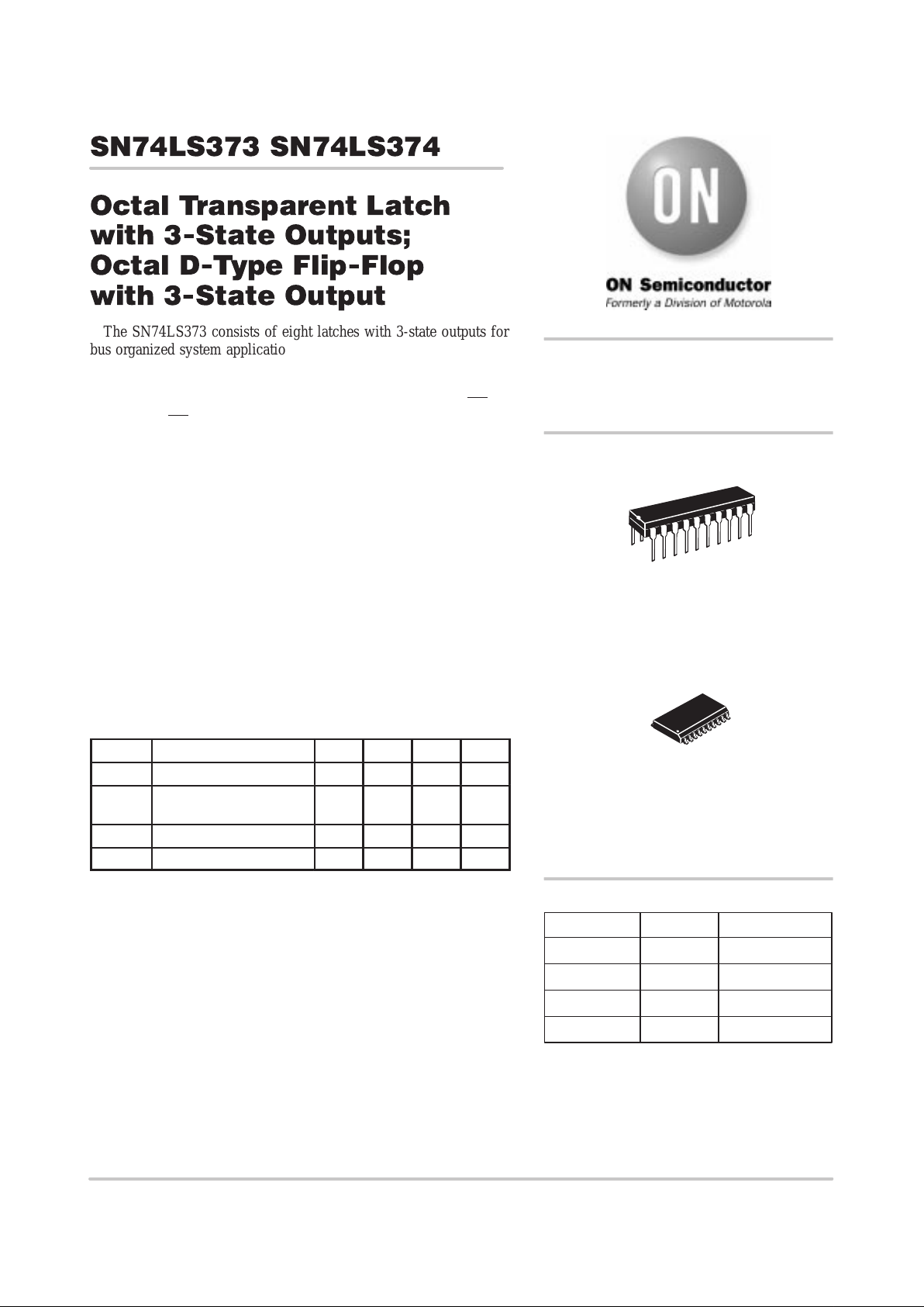
ORDERING INFORMATION
SN74LS373N 16 Pin DIP 1440 Units/Box
SN74LS373DW 16 Pin
SOIC
DW SUFFIX
CASE 751D
http://onsemi.com
2500/Tape & Reel
PLASTIC
N SUFFIX
CASE 738
20
1
20
1
SN74LS374N 16 Pin DIP 1440 Units/Box
SN74LS374DW 16 Pin
2500/Tape & Reel
SN74LS373 SN74LS374
http://onsemi.com
2
CONNECTION DIAGRAM DIP (TOP VIEW)
Data Inputs
Latch Enable (Active HIGH) Input
Clock (Active HIGH Going Edge) Input
Output Enable (Active LOW) Input
Outputs
D
0
– D
7
LE
CP
OE
O0 – O
7
0.5 U.L.
0.5 U.L.
0.5 U.L.
0.5 U.L.
65 U.L.
0.25 U.L.
0.25 U.L.
0.25 U.L.
0.25 U.L.
15 U.L.
NOTES:
a) 1 TTL Unit Load (U.L.) = 40 mA HIGH/1.6 mA LOW.
HIGH LOW
(Note a)
LOADING
PIN NAMES
NOTE:
The Flatpak version
has the same pinouts
(Connection Diagram) as
the Dual In-Line Package.
SN74LS373
SN74LS374
18 17 16 15 14 13
1234 56
7
20 19
8
V
CC
OE
O7D7D6O
6
D
5
O
5
D
4
O0D0D1O1O2D2D
3
910
O
3
GND
12
O
4
LE
18 17 16 15 14 13
123456
7
20 19
8
V
CC
OE
O7D7D6O
6
D
5
O
5
D
4
O0D0D1O1O2D2D
3
910
O
3
GND
12 11
O
4
CP
11
TRUTH TABLE
LS373
D
n
LE OE O
n
H H L H
L H L L
X L L Q
0
X X H Z*
LS374
D
n
LE OE O
n
H L H
L L L
X X H Z*
H = HIGH Voltage Level
L = LOW Voltage Level
X = Immaterial
Z = High Impedance
* Note: Contents of flip-flops unaffected by the state of the Output Enable input (OE
).
SN74LS373 SN74LS374
http://onsemi.com
3
LOGIC DIAGRAMS
SN74LS373
SN74LS374
D
D
G
Q
CP
QQ
CP
OE
OE
LE
LATCH
ENABLE
O
0
O
1
O
2
O
3
O
4
O
5
O
6
O
7
D
0
14
1
26
73 84
5 9
11
12 16
13
15
VCC = PIN 20
GND = PIN 10
= PIN NUMBERS
D
G
Q
D
1
D
G
Q
D
2
D
G
Q
D
3
D
G
Q
D
4
D
G
Q
D
5
D
G
Q
D
6
D
G
Q
D
7
17 18
19
O
0
O
1
O
2
O
3
O
4
O
5
O
6
O
7
265 9 12 1615 19
D
0
1473 84 13
D
1
D
2
D
3
D
4
D
5
D
6
D
7
17 18
1
11
DCP
QQ
DCP
QQ
DCP
QQ
DCP
QQ
DCP
QQ
DCP
QQ
DCP
QQ
DC CHARACTERISTICS OVER OPERATING TEMPERATURE RANGE (unless otherwise specified)
Limits
Symbol Parameter
Min Typ Max
Unit Test Conditions
V
IH
Input HIGH Voltage 2.0 V
Guaranteed Input HIGH Voltage for
All Inputs
V
IL
Input LOW Voltage
0.8
V
Guaranteed Input LOW Voltage for
All Inputs
V
IK
Input Clamp Diode Voltage –0.65 –1.5 V VCC = MIN, IIN = –18 mA
V
OH
Output HIGH Voltage 2.4 3.1 V
VCC = MIN, IOH = MAX, VIN = V
IH
or VIL per Truth Table
p
0.25 0.4 V IOL = 12 mA
VCC = VCC MIN,
VOLOutput LOW Voltage
0.35 0.5 V IOL = 24 mA
V
IN
=
V
IL
or
V
IH
per Truth Table
I
OZH
Output Off Current HIGH 20 µA VCC = MAX, V
OUT
= 2.7 V
I
OZL
Output Off Current LOW –20 µA VCC = MAX, V
OUT
= 0.4 V
p
20 µA VCC = MAX, VIN = 2.7 V
IIHInput HIGH Current
0.1 mA VCC = MAX, VIN = 7.0 V
I
IL
Input LOW Current –0.4 mA VCC = MAX, VIN = 0.4 V
I
OS
Short Circuit Current (Note 1) –30 –130 mA VCC = MAX
I
CC
Power Supply Current 40 mA VCC = MAX
Note 1: Not more than one output should be shorted at a time, nor for more than 1 second.
 Loading...