

Page 1

Freescale Semiconductor, Inc.
EC000 Core Processor
nc...
, I
or
emiconduct
eescale S
Fr
(SCM68000)
User’s Manual
Motorola reserves the right to make changes without further notice to any products herein. Motorola makes no warranty, representation or guarantee regarding
the suitability of its products for any particular purpose, nor does Motorola assume any liability arising out of the application or use of any product or circuit, and
specifically disclaims any and all liability, including without limitation consequential or incidental damages. "Typical" parameters can and do vary in different
applications. All operating parameters, including "Typicals" must be validated for each customer application by customer's technical experts. Motorola does not
convey any license under its patent rights nor the rights of others. Motorola products are not designed, intended, or authorized for use as components in systems
intended for surgical implant into the body, or other applications intended to support or sustain life, or for any other application in which the failure of the Motorola
product could create a situation where personal injury or death may occur. Should Buyer purchase or use Motorola products for any such unintended or
unauthorized application, Buyer shall indemnify and hold Motorola and its officers, employees, subsidiaries, affiliates, and distributors harmless against all claims,
costs, damages, and expenses, and reasonable attorney fees arising out of, directly or indirectly, any claim of personal injury or death associated with such
unintended or unauthorized use, even if such claim alleges that Motorola was negligent regarding the design or manufacture of the part. Motorola and are
registered trademarks of Motorola, Inc. Motorola, Inc. is an Equal Opportunity/Affirmative Action Employer.
MOTOROLA, 1995
For More Information On This Product,
Go to: www.freescale.com
µ
Page 2

nc...
, I
Freescale Semiconductor, Inc.
68K FAX-IT
Documentation Comments
FAX 512-891-8593—Documentation Comments Only
The Motorola High-Performance Embedded Systems Technical Communications Department provides a fax number for you to submit any questions or comments about this document or how to order other documents. We welcome your suggestions for improving our
documentation. Please do not fax technical questions.
Please provide the part number and revision number (located in upper right-hand corner of
the cover) and the title of the document. When referring to items in the manual, please reference by the page number, paragraph number, figure number, table number, and line number if needed.
or
emiconduct
eescale S
Fr
When sending a fax, please provide your name, company, fax number, and phone number
including area code.
Applications and Technical Information
For questions or comments pertaining to technical information, questions, and applications,
please contact one of the following sales offices nearest you.
MOTOROLA
EC000 CORE PROCESSOR USER’S MANUAL
For More Information On This Product,
Go to: www.freescale.com
iii
Page 3

iv
Freescale Semiconductor, Inc.
— Sales Offices —
Field Applications Engineering Available Through All Sales Offices
nc...
, I
or
emiconduct
eescale S
Fr
ALABAMA , Huntsville (205) 464-6800
UNITED STATES
ARIZONA , Tempe (602) 897-5056
CALIFORNIA , Agoura Hills (818) 706-1929
CALIFORNIA , Los Angeles (310) 417-8848
CALIFORNIA , Irvine (714) 753-7360
CALIFORNIA , Rosevllle (916) 922-7152
CALIFORNIA , San Diego (619) 541-2163
CALIFORNIA , Sunnyvale (408) 749-0510
COLORADO , Colorado Springs (719) 599-7497
COLORADO , Denver (303) 337-3434
CONNECTICUT , Wallingford (203) 949-4100
FLORIDA , Maitland (407) 628-2636
FLORIDA , Pompano Beach/
Fort Lauderdale (305) 486-9776
FLORIDA , Clearwater (813) 538-7750
GEORGlA , Atlanta (404) 729-7100
IDAHO , Boise (208) 323-9413
ILLINOIS , Chicago/Hoffman Estates (708) 490-9500
INDlANA , Fort Wayne (219) 436-5818
INDIANA , Indianapolis (317) 571-0400
INDIANA , Kokomo (317) 457-6634
IOWA , Cedar Rapids (319) 373-1328
KANSAS , Kansas City/Mission (913) 451-8555
MARYLAND , Columbia (410) 381-1570
MASSACHUSETTS , Marborough (508) 481-8100
MASSACHUSETTS , Woburn (617) 932-9700
MICHIGAN , Detroit (313) 347-6800
MINNESOTA , Minnetonka (612) 932-1500
MISSOURI , St. Louis (314) 275-7380
NEW JERSEY , Fairfield (201) 808-2400
NEW YORK , Fairport (716) 425-4000
NEW YORK , Hauppauge (516) 361-7000
NEW YORK , Poughkeepsie/Fishkill (914) 473-8102
NORTH CAROLINA , Raleigh (919) 870-4355
OHIO , Cleveland (216) 349-3100
OHIO , Columbus/Worthington (614) 431-8492
OHIO , Dayton (513) 495-6800
OKLAHOMA , Tulsa (800) 544-9496
OREGON , Portland (503) 641-3681
PENNSYLVANIA , Colmar (215) 997-1020
Philadelphia/Horsham (215) 957-4100
TENNESSEE , Knoxville (615) 690-5593
TEXAS , Austin (512) 873-2000
TEXAS , Houston (800) 343-2692
TEXAS , Plano (214) 516-5100
VIRGINIA , Richmond (804) 285-2100
WASHINGTON , Bellevue (206) 454-4160
Seattle Access (206) 622-9960
WISCONSIN , Milwaukee/Brookfield (414) 792-0122
BRITISH COLUMBIA , Vancouver (604) 293-7605
ONTARIO , Toronto (416) 497-8181
ONTARIO , Ottawa (613) 226-3491
QUEBEC , Montreal (514) 731-6881
AUSTRALIA , Melbourne (61-3)887-0711
AUSTRALIA , Sydney (61(2)906-3855
BRAZIL , Sao Paulo 55(11)815-4200
CHINA , Beijing 86 505-2180
FINLAND , Helsinki 358-0-35161191
Car Phone 358(49)211501
FRANCE , Paris/Vanves 33(1)40 955 900
CANADA
INTERNATIONAL
GERMANY , Langenhagen/ Hanover 49(511)789911
GERMANY , Munich 49 89 92103-0
GERMANY , Nuremberg 49 911 64-3044
GERMANY , Sindelfingen 49 7031 69 910
GERMANY , Wiesbaden 49 611 761921
HONG KONG , Kwai Fong 852-4808333
Tai Po 852-6668333
INDIA , Bangalore (91-812)627094
ISRAEL , Tel Aviv 972(3)753-8222
ITALY , Milan 39(2)82201
JAPAN , Aizu 81(241)272231
JAPAN , Atsugi 81(0462)23-0761
JAPAN , Kumagaya 81(0485)26-2600
JAPAN , Kyushu 81(092)771-4212
JAPAN , Mito 81(0292)26-2340
JAPAN , Nagoya 81(052)232-1621
JAPAN , Osaka 81(06)305-1801
JAPAN, Sendai 81(22)268-4333
JAPAN,
JAPAN,
JAPAN
KOREA , Pusan 82(51)4635-035
KOREA , Seoul 82(2)554-5188
MALAYSIA , Penang 60(4)374514
MEXICO , Mexico City 52(5)282-2864
MEXICO , Guadalajara 52(36)21-8977
Marketing 52(36)21-9023
Customer Service 52(36)669-9160
NETHERLANDS , Best (31)49988 612 11
PUERTO RICO , San Juan (809)793-2170
SINGAPORE
SPAIN , Madrid 34(1)457-8204
or 34(1)457-8254
SWEDEN , Solna 46(8)734-8800
SWITZERLAND , Geneva 41(22)7991111
SWITZERLAND , Zurich 41(1)730 4074
TAlWAN , Taipei 886(2)717-7089
THAILAND , Bangkok (66-2)254-4910
UNITED KINGDOM , Aylesbury 44(296)395-252
COLORADO , Grand Junction
Cheryl Lee Whltely (303) 243-9658
KANSAS , Wichita
Melinda Shores/Kelly Greiving (316) 838 0190
NEVADA , Reno
Galena Technology Group (702) 746 0642
NEW MEXICO , Albuquerque
S&S Technologies, lnc. (505) 298-7177
UTAH , Salt Lake City
Utah Component Sales, Inc. (801) 561-5099
WASHINGTON , Spokane
Doug Kenley (509) 924-2322
ARGENTINA , Buenos Aires
Argonics, S.A. (541) 343-1787
Elmo Semiconductor (818) 768-7400
Minco Technology Labs Inc. (512) 834-2022
Semi Dice Inc. (310) 594-4631
Tachikawa 81(0425)23-6700
Tokyo 81(03)3440-3311
, Yokohama 81(045)472-2751
(65)2945438
FULL LINE REPRESENTATIVES
HYBRID COMPONENTS RESELLERS
EC000 CORE PROCESSOR USER’S MANUAL
For More Information On This Product,
Go to: www.freescale.com
MOTOROLA
Page 4

Freescale Semiconductor, Inc.
PREFACE
The
EC000 Core Processor User's Manual
operation of the SCM68000 (EC000 core); the
Manual
vides a brief description of the FlexCore program.
The organization of this manual is as follows:
provides instruction details for the EC000 core; and the
Section 1 Overview
Section 2 Signal Description
Section 3 Bus Operation
Section 4 Exception Processing
Section 5 8-Bit Instruction Execution Times
describes the programming, capabilities, and
MC68000 Family Programmer’s Reference
FlexCore Product Brief
pro-
nc...
, I
or
emiconduct
eescale S
Fr
Section 6 16-Bit Instruction Execution Times
Section 7 Electrical Characteristics
TRADEMARKS
• Composer, Verilog, Verifault, and Veritime are trademarks of Cadence Design Systems, Inc.
• Synopsys is a registered trademark of Synopsys, Inc.
• TDS is a registered trademark of Summit Design, Inc.
MOTOROLA
EC000 CORE PROCESSOR USER’S MANUAL
For More Information On This Product,
Go to: www.freescale.com
v
Page 5

Freescale Semiconductor, Inc.
nc...
, I
or
emiconduct
eescale S
Fr
vi EC000 CORE PROCESSOR USER’S MANUAL MOTOROLA
For More Information On This Product,
Go to: www.freescale.com
Page 6

Freescale Semiconductor, Inc.
TABLE OF CONTENTS
Section 1
Overview
1.1 FlexCore Integrated Processors...................................................................1-2
1.1.1 FlexCore Advantages .................................................................................1-4
1.1.2 FlexCore Module Types..............................................................................1-4
1.2 Development Cycle.......................................................................................1-5
1.3 Programming Model......................................................................................1-7
1.4 Data Types and Addressing Modes..............................................................1-9
nc...
, I
or
1.5 Data Organization.......................................................................................1-10
1.5.1 Data Registers..........................................................................................1-10
1.5.2 Address Registers ....................................................................................1-10
1.5.3 Data Organization In Memory...................................................................1-10
1.6 Instruction Set Summary.............................................................................1-11
emiconduct
eescale S
Fr
Section 2
Signal Description
2.1 Address Bus (A31–A0) .................................................................................2-1
2.2 Data Bus (D15–D0).......................................................................................2-1
2.3 Clock (CLKI, CLKO)......................................................................................2-1
2.4 Asynchronous Bus Control ...........................................................................2-3
2.4.1 Address Strobe (ASB) ................................................................................2-3
2.4.2 Read/Write (RWB) and Early Read/Write (ERWB).....................................2-3
2.4.3 Upper and Lower Data Strobes (UDSB, LDSB), and Data Strobe (DSB) ..2-4
2.4.4 Data Transfer Acknowledge (DTACKB) .....................................................2-4
2.4.5 Data Transfer Size (SIZ1–SIZ0) .................................................................2-4
2.4.6 Read-Modify-Write (RMCB)........................................................................2-5
2.5 Bus Arbitration Control..................................................................................2-5
2.5.1 Bus Request (BRB) ....................................................................................2-5
2.5.2 Bus Grant (BGB).........................................................................................2-5
2.5.3 Bus Grant Acknowledge (BGACKB)—3-Wire Protocol Only......................2-5
2.6 Interrupt Control (IPLB2–IPLB0)...................................................................2-5
2.7 System Control .............................................................................................2-6
2.7.1 Bus Error (BERRB).....................................................................................2-6
2.7.2 Reset External/Internal (RESETIB, RESETOB) .........................................2-6
2.7.3 Halt External/Internal (HALTIB, HALTOB)..................................................2-6
2.7.4 Mode (MODE).............................................................................................2-7
2.7.5 Disable Control (DISB) ...............................................................................2-7
2.7.6 Test Mode (TEST) ......................................................................................2-7
2.7.7 Test Clock (TESTCLK) ...............................................................................2-7
2.7.8 Autovector (AVECB)...................................................................................2-8
MOTOROLA
EC000 CORE PROCESSOR USER’S MANUAL
For More Information On This Product,
Go to: www.freescale.com
vii
Page 7

Table of Contents
2.8 Three-State Control...................................................................................... 2-8
2.8.1 Address Output Enable (AOEB).................................................................2-8
2.8.2 Control Output Enable (COEB) ..................................................................2-8
2.8.3 Data Output Enable (DOEB) ......................................................................2-8
2.9 Processor Status ..........................................................................................2-8
2.9.1 Function Codes (FC2–FC0) .......................................................................2-8
2.9.2 Address Three-State Control (TSCAE) ......................................................2-9
2.9.3 Stop Instruction Indicator (STOP)...............................................................2-9
2.9.4 Interrupt Pending (IPENDB) ....................................................................... 2-9
2.9.5 CPU Pipe Refill (REFILLB).........................................................................2-9
2.9.6 Microsequencer Status Indication (STATUSB) ..........................................2-9
2.10 Multiplexing Pins...........................................................................................2-9
nc...
Freescale Semiconductor, Inc.
Section 3
Bus Operation
, I
or
emiconduct
eescale S
Fr
3.1 Data Transfer Operations............................................................................. 3-1
3.1.1 Read Cycle.................................................................................................3-2
3.1.2 Write Cycle .................................................................................................3-8
3.1.3 Read-Modify-Write Cycle..........................................................................3-13
3.2 Bus Arbitration............................................................................................3-17
3.2.1 Requesting the Bus .................................................................................. 3-18
3.2.2 Receiving the Bus Grant...........................................................................3-18
3.2.3 Acknowledgment of Mastership (3-Wire Bus Arbitration Only).................3-19
3.3 Bus Arbitration Control................................................................................ 3-22
3.4 Bus Error and Halt Operation .....................................................................3-30
3.4.1 Bus Error Operation..................................................................................3-30
3.4.2 Retrying the Bus Cycle.............................................................................3-32
3.4.3 Halt Operation ..........................................................................................3-32
3.4.4 Double Bus Fault......................................................................................3-35
3.5 Asynchronous Operation............................................................................3-35
3.6 Synchronous Operation..............................................................................3-38
3.7 The Relationship of DTACKB, BERRB, and HALTIB.................................3-42
Section 4
Exception Processing
4.1 Privilege Modes............................................................................................ 4-1
4.1.1 Supervisor Mode ........................................................................................4-2
4.1.2 User Mode..................................................................................................4-2
4.1.3 Privilege Mode Changes ............................................................................4-2
4.1.4 Reference Classification............................................................................. 4-3
4.1.5 CPU Space Cycle....................................................................................... 4-3
4.1.5.1 Interrupt Acknowledge Cycle.................................................................... 4-3
4.1.5.2 Autovectored Interrupt Acknowledge Cycle .............................................4-7
4.2 Exception Processing Description..............................................................4-11
4.2.1 Exception Vectors.....................................................................................4-11
viii
EC000 CORE PROCESSOR USER’S MANUAL
For More Information On This Product,
Go to: www.freescale.com
MOTOROLA
Page 8

nc...
, I
or
4.2.2 Kinds of Exceptions ..................................................................................4-13
4.2.3 Multiple Exceptions...................................................................................4-13
4.2.4 Exception Stack Frames...........................................................................4-14
4.2.5 Exception Processing Sequence..............................................................4-14
4.3 Processing of Specific Exceptions..............................................................4-15
4.3.1 Reset ........................................................................................................4-15
4.3.1.1 Reset Operation .....................................................................................4-16
4.3.1.1.1 Reset Using RESETIB and HALTIB.....................................................4-16
4.3.1.1.2 Reset Instruction...................................................................................4-16
4.3.1.1.3 Reset Using Only RESETIB.................................................................4-17
4.3.1.2 Initializing the SCM68000 for Simulation................................................4-18
4.3.2 Interrupts...................................................................................................4-19
4.3.2.1 Level Seven Interrupts............................................................................4-20
4.3.2.2 Uninitialized Interrupt..............................................................................4-20
4.3.2.3 Spurious Interrupt...................................................................................4-20
4.3.3 Instruction Traps.......................................................................................4-21
4.3.4 Illegal and Unimplemented Instructions....................................................4-21
4.3.5 Privilege Violations ...................................................................................4-21
4.3.6 Tracing......................................................................................................4-22
4.3.7 Bus Error...................................................................................................4-22
4.3.8 Address Error............................................................................................4-23
Freescale Semiconductor, Inc.
Table of Contents
emiconduct
eescale S
Fr
Section 5
8-Bit Instruction Execution Times
5.1 Operand Effective Address Calculation Times .............................................5-1
5.2 MOVE Instruction Execution Times..............................................................5-2
5.3 Standard Instruction Execution Times..........................................................5-3
5.4 Immediate Instruction Execution Times........................................................5-4
5.5 Single Operand Instruction Execution Times................................................5-5
5.6 Shift/Rotate Instruction Execution Times......................................................5-6
5.7 Bit Manipulation Instruction Execution Timess .............................................5-6
5.8 Conditional Instruction Execution Times.......................................................5-6
5.9 JMP, JSR, LEA, PEA, and MOVEM Instruction Execution Times................5-7
5.10 Multiprecision Instruction Execution Times...................................................5-7
5.11 Miscellaneaous Instruction Execution Times................................................5-8
5.12 Exception Processing Execution Times........................................................5-9
Section 6
16-Bit Instruction Execution Times
6.1 Operand Effective Address Calculation Times .............................................6-1
6.2 MOVE Instruction Execution Times..............................................................6-2
6.3 Standard Instruction Execution Times..........................................................6-3
6.4 Immediate Instruction Execution Times........................................................6-4
6.5 Single Operand Instruction Execution Times................................................6-5
6.6 Shift/Rotate Instruction Execution Times......................................................6-6
MOTOROLA
EC000 CORE PROCESSOR USER’S MANUAL
For More Information On This Product,
Go to: www.freescale.com
ix
Page 9

nc...
, I
or
x
Table of Contents
6.7 Bit Manipulation Instruction Execution Times...............................................6-6
6.8 Conditional Instruction Execution Times....................................................... 6-7
6.9 JMP, JSR, LEA, PEA, and MOVEM Instruction Execution Times................6-7
6.10 Multiprecision Instruction Execution Times................................................... 6-7
6.11 Miscellaneous Instruction Execution Times..................................................6-8
6.12 Exception Processing Execution Times........................................................ 6-9
7.1 Maximum Ratings.........................................................................................7-1
7.2 CMOS Considerations..................................................................................7-1
7.3 Power Consumption .....................................................................................7-1
7.4 AC Electrical Specification Definitions..........................................................7-1
7.5 AC Electrical Specifications—Clock Timing.................................................. 7-2
7.6 AC Electrical Specifications—Read and Write Cycles.................................. 7-2
7.7 AC Electrical Specifications—SCM68000 to External Peripherals...............7-6
7.8 AC Electrical Specifications—Bus Arbitration............................................... 7-7
7.9 AC Electrical Specifications—Core Applications Signals ...........................7-11
Freescale Semiconductor, Inc.
Section 7
Electrical Characteristics
emiconduct
eescale S
Fr
EC000 CORE PROCESSOR USER’S MANUAL
For More Information On This Product,
Go to: www.freescale.com
MOTOROLA
Page 10

Freescale Semiconductor, Inc.
LIST OF ILLUSTRATIONS
1-1 FlexCore Integrated Processor Typical Die Layout............................................1-3
1-2 Standard Cell Design Flow.................................................................................1-6
1-3 Programming Model...........................................................................................1-7
1-4 Status Register...................................................................................................1-8
1-5 Word Organization in Memory..........................................................................1-10
1-6 Data Organization in Memory...........................................................................1-12
2-1 Input/Output Signals...........................................................................................2-2
3-1 Word Read Cycle Flowchart for 16-Bit Mode.....................................................3-2
nc...
, I
or
emiconduct
eescale S
Fr
3-2 Byte Read Cycle Flowchart for 8-Bit Mode ........................................................3-3
3-3 Byte Read Cycle Flowchart for 16-Bit Mode ......................................................3-3
3-4 Read and Write Cycle Timing Diagram for 8-Bit Mode ......................................3-4
3-5 Read and Write Cycle Timing Diagram for 16-Bit Mode ....................................3-5
3-6 Word and Byte Read Cycle Timing Diagram for 16-Bit Mode............................3-6
3-7 Word Write Cycle Flowchart for 16-Bit Mode.....................................................3-8
3-8 Byte Write Cycle Flowchart for 8-Bit Mode.........................................................3-9
3-9 Byte Write Cycle Flowchart for 16-Bit Mode.......................................................3-9
3-10 Write Cycle Timing Diagram for 8-Bit Mode.....................................................3-10
3-11 Word and Byte Write Cycle Timing Diagram for 16-Bit Mode..........................3-11
3-12 Read-Modify-Write Cycle Flowchart.................................................................3-13
3-13 Read-Modify-Write Cycle Timing Diagram.......................................................3-14
3-14 3-Wire Bus Arbitration Cycle Flowchart............................................................3-18
3-15 2-Wire Bus Arbitration Cycle Flowchart............................................................3-19
3-16 3-Wire Bus Arbitration Timing Diagram............................................................3-20
3-17 2-Wire Bus Arbitration Timing Diagram............................................................3-21
3-18 Bus Arbitration Unit State Diagrams.................................................................3-23
3-19 3-Wire Bus Arbitration Timing Diagram—SCM68000 Active ...........................3-24
3-20 3-Wire Bus Arbitration Timing Diagram—Bus Inactive.....................................3-25
3-21 3-Wire Bus Arbitration Timing Diagram—Special Case...................................3-26
3-22 2-Wire Bus Arbitration Timing Diagram—SCM68000 Active ...........................3-27
3-23 2-Wire Bus Arbitration Timing Diagram—Bus Inactive.....................................3-28
3-24 2-Wire Bus Arbitration Timing Diagram—Special Case...................................3-29
3-25 Bus Error Timing Diagram................................................................................3-31
3-26 Retry Bus Cycle Timing Diagram.....................................................................3-33
3-27 Halt Operation Timing Diagram........................................................................3-34
3-28 External Asynchronous Signal Synchronization...............................................3-35
3-29 Fully Asynchronous Read Cycle ......................................................................3-36
3-30 Fully Asynchronous Write Cycle.......................................................................3-36
3-31 Pseudo-Asynchronous Read Cycle..................................................................3-37
3-32 Pseudo-Asynchronous Write Cycle..................................................................3-38
MOTOROLA
EC000 CORE PROCESSOR USER’S MANUAL
For More Information On This Product,
Go to: www.freescale.com
xi
Page 11

nc...
, I
or
emiconduct
List of Illustrations
3-33 Synchronous Read Cycle................................................................................. 3-39
3-34 Synchronous Write Cycle.................................................................................3-40
4-1 CPU Space Address Encoding..........................................................................4-3
4-2 Interrupt Acknowledge Cycle Timing Diagram...................................................4-4
4-3 Autovector Operation Timing Diagram...............................................................4-8
4-4 Autovector Operation Timing Diagram—Best Case........................................... 4-9
4-5 Autovector Operation Timing Diagram—Worst Case ......................................4-10
4-6 Exception Vector Format.................................................................................. 4-11
4-7 Address Translated from 8-Bit Vector Number................................................4-11
4-8 Interrupt Vector Number Format......................................................................4-13
4-9 Groups 1 and 2 Exception Stack Frame..........................................................4-15
4-10 Reset Circuit..................................................................................................... 4-16
4-11 Reset Operation Timing Diagram..................................................................... 4-17
4-12 RESETOB Timing Diagram.............................................................................. 4-18
4-13 Initialization of the SCM68000 for Simulation Timing Diagram........................4-19
4-14 Supervisor Stack Order for Bus or Address Error Exception...........................4-23
7-1 Clock Input Timing Diagram...............................................................................7-2
7-2 Read Cycle Timing Diagram..............................................................................7-4
7-3 Write Cycle Timing Diagram ..............................................................................7-5
7-4 SCM68000 to External Peripherals Timing Diagram .........................................7-6
7-5 Bus Arbitration Timing Diagram.........................................................................7-7
7-6 Bus Arbitration Timing Diagram—Idle Bus Case...............................................7-8
7-7 Bus Arbitration Timing Diagram—Active Bus Case...........................................7-9
7-8 Bus Arbitration Timing Diagram—Multiple Bus Request.................................. 7-10
7-9 Core Application Signals Timing Diagram........................................................ 7-12
Freescale Semiconductor, Inc.
eescale S
Fr
xii
EC000 CORE PROCESSOR USER’S MANUAL
For More Information On This Product,
Go to: www.freescale.com
MOTOROLA
Page 12

Freescale Semiconductor, Inc.
LIST OF TABLES
1-1 Data Addressing Modes.....................................................................................1-9
1-2 Notational Conventions....................................................................................1-13
1-3 Instruction Set Summary..................................................................................1-14
2-1 Signal Summary.................................................................................................2-2
2-2 Upper and Lower Data Strobe Control of Data Bus...........................................2-4
2-3 Lower Data Strobe Control of Data Bus.............................................................2-4
2-4 Data Transfer Size .............................................................................................2-5
2-5 Interrupt Levels and Mask Values......................................................................2-6
2-6 Function Code Outputs ......................................................................................2-8
nc...
, I
or
emiconduct
eescale S
Fr
2-7 Status Indication Exceptions..............................................................................2-9
2-8 Pin Multiplexing Priority....................................................................................2-10
3-1 DTACKB, BERRB, and HALTIB Assertion Results..........................................3-43
3-2 BERRB and HALTIB Negation Results............................................................3-44
4-1 Reference Classification.....................................................................................4-3
4-2 Exception Vector Assignment ..........................................................................4-12
4-3 Exception Grouping and Priority.......................................................................4-14
5-1 Effective Address Calculation Times..................................................................5-2
5-2 Move Byte Instruction Execution Times.............................................................5-2
5-3 Move Word Instruction Execution Times............................................................5-3
5-4 Move Long Instruction Execution Times ............................................................5-3
5-5 Standard Instruction Execution Times................................................................5-4
5-6 Immediate Instruction Execution Times .............................................................5-5
5-7 Single Operand Instruction Execution Times.....................................................5-5
5-8 Shift/Rotate Instruction Execution Times ...........................................................5-6
5-9 Bit Manipulation Instruction Execution Times.....................................................5-6
5-10 Conditional Instruction Execution Times............................................................5-7
5-11 JMP, JSR, LEA, PEA, and MOVEM Instruction Execution Times......................5-7
5-12 Multiprecision Instruction Execution Times........................................................5-8
5-13 Miscellaneous Instruction Execution Times .......................................................5-8
5-14 Move Peripheral Instruction Execution Times....................................................5-9
5-15 Exception Processing Execution Times.............................................................5-9
6-1 Effective Address Calculation Times..................................................................6-2
6-2 Move Byte and Word Instruction Execution Times.............................................6-2
6-3 Move Long Instruction Execution Times ............................................................6-3
6-4 Standard Instruction Execution Times................................................................6-4
6-5 Immediate Instruction Execution Times .............................................................6-5
6-6 Single Operand Instruction Execution Times.....................................................6-5
6-7 Shift/Rotate Instruction Execution Times ...........................................................6-6
6-8 Bit Manipulation Instruction Execution Times.....................................................6-6
6-9 Conditional Instruction Execution Times............................................................6-7
MOTOROLA
EC000 CORE PROCESSOR USER’S MANUAL
For More Information On This Product,
Go to: www.freescale.com
xiii
Page 13

List of Tables
6-10 JMP, JSR, LEA, PEA, and MOVEM Instruction Execution Times .....................6-7
6-11 Multiprecision Instruction Execution Times........................................................6-8
6-12 Miscellaneous Instruction Execution Times.......................................................6-8
6-13 Move Peripheral Instruction Execution Times....................................................6-9
6-14 Exception Processing Execution Times.............................................................6-9
Freescale Semiconductor, Inc.
nc...
, I
or
emiconduct
eescale S
Fr
xiv
EC000 CORE PROCESSOR USER’S MANUAL
For More Information On This Product,
Go to: www.freescale.com
MOTOROLA
Page 14

Freescale Semiconductor, Inc.
SECTION 1
OVERVIEW
nc...
, I
or
emiconduct
eescale S
This document contains a summary of the use and operation of the SCM68000 microprocessor core (also referred to as the EC000 core)
specifications. Refer to the
(M68000UM/AD) for detailed information on the operation of the instruction set, addressing
modes, and bus architecture for this core.
The SCM68000 is a core implementation of the MC68000 32-bit microprocessor and is
designed to be used as part of the FlexCore Program. In the FlexCore program, high-volume
manufacturers can create their own integrated microprocessor containing a core processor,
such as the SCM68000, and their own proprietary technology. A FlexCore integrated processor allows significant reductions in component count, power consumption, board space,
and cost while yielding much higher system reliability and performance.
The main features of the SCM68000 include:
• Low-Power HCMOS Implementation Requires Only 15 mA at 3.3 V
• 32-Bit Performance for 16-Bit Applications—2.7 MIPS at 16 MHz
• Statically Selectable 8-Bit or 16-Bit Data Bus Operation
• 32-Bit Address Bus Directly Addresses up to 4 Gbytes of Address Space
• Static Operation Provides Almost Zero Power Consumption During Idle Periods
• Sixteen General-Purpose 32-Bit Data and Address Registers
• Fifty-Six Powerful Instruction Types That Support High-Level Programming Languages
• Fourteen Addressing Modes and Five Main Data Types Allow Compact, Efficient Code
• Seven Priority Level Interrupt Control
M68000 8-/16-/32-Bit Microprocessor User’s Manual
1
and a detailed set of timing and electrical
Fr
• Special Core Interfacing Signals
• Emulation Support Signals Including Pipeline Refill, Processor Status, and Interrupt
Pending Signals
• Both 3.3-V and 5-V Operation
The SCM68000 has a statically selectable 8-bit or 16-bit data bus. The address bus is 32bits wide and may be used as either a 24-bit address bus as on the MC68000 microprocessors, or as a 32-bit address bus to fully support the internal architecture. The 32-bit address
1.
The SCM68000 is the name of the Verilog model for the EC000 core. The remainder of this section
will refer to the EC000 core as only the SCM68000.
MOTOROLA
EC000 CORE PROCESSOR USER’S MANUAL
For More Information On This Product,
Go to: www.freescale.com
1-1
Page 15

Overview
bus allows direct addressing of up to 4 Gbytes. Logic can be added to implement dynamic
bus sizing.
The SCM68000 is upward code compatible with all other members of the M68000 microprocessor family. Any user-mode programs using the SCM68000 instruction set will run
unchanged on any MC680x0, MC68EC0x0, or MC683xx processor. This is possible
because the user programming model is identical for all processors and the instruction sets,
addressing modes, and data types for the SCM68000 are proper subsets of the complete
architecture.
The SCM68000 also includes some functions not found on the standard MC68000 and
MC68EC000 microprocessors such as the processor status, pipeline refill, and interrupt
pending signals. These signals permit emulation support and facilitate interfacing between
the SCM68000 and on-chip logic.
Freescale Semiconductor, Inc.
1.1 FLEXCORE INTEGRATED PROCESSORS
nc...
, I
or
emiconduct
eescale S
Fr
FlexCore allows designers of high-volume digital systems and third-party technology providers to place their proprietary circuitry on chip with a Motorola microprocessor. By using FlexCore, a designer can reduce the total system cost, component count, and power
consumption while providing higher performance and greater reliability. Up to 100,000 gates
or more of custom logic, memory, and peripheral modules can be added to a core processor
to produce the most cost-effective solution for a designer's system. The core processors
provide special power-management features such as 5 V, 3.3 V, and static operation. The
68000 Family of core processors offers the designer a range of performance from 3 to 12
million instructions per second (MIPS) (to be extended to 100 MIPS) while maintaining complete code compatibility throughout the Family. The 68000 processors have a proven architecture with a broad base of application and system software support, including real-time
kernels, operating systems, and compilers, in addition to a wide range of tools to support
software development. In the future, additional processing architectures will be included in
the FlexCore program, including PowerPC
1 shows a typical die layout for a FlexCore integrated processor.
Complete product lines can be created using FlexCore by implementing one base design
using a variety of core processors. Designers already familiar with 68000 Family design can
easily migrate to FlexCore processors as the core processors use the same bus interfaces
found on the standard 68000 Family members. Additionally, many peripheral modules and
memory elements are available for integration. Motorola has developed a complete design
system to put into the hands of the customer that includes both a broad cell-based library
and effective computer-aided design (CAD) tools. By building on Motorola's proven 68000
microprocessor architecture and superior manufacturing capabilities, FlexCore offers
designers the best path to higher system integration.
and digital signal processing (DSP). Figure 1-
1-2
EC000 CORE PROCESSOR USER’S MANUAL
For More Information On This Product,
Go to: www.freescale.com
MOTOROLA
Page 16

Freescale Semiconductor, Inc.
Overview
nc...
, I
or
CUSTOMER-DESIGNED
LOGIC
SPECIAL-FUNCTION
BLOCK/
MEMORY BLOCK
SPECIAL-FUNCTION
BLOCK/
MEMORY BLOCK
68000 FAMILY
PROCESSOR
Figure 1-1. FlexCore Integrated Processor Typical Die Layout
FlexCore custom processors are ideal for:
• High-volume users of 8-, 16-, and 32-bit integrated solutions requiring higher system
performance whose needs are not met by standard 68300 Family devices.
• Designers of high-volume applications who need to reduce cost, space, and/or power
consumption.
• Third-party technology providers who want to deliver their proprietary application-specific technology to a worldwide marketplace.
emiconduct
To develop a solution that best suits system requirements in the shortest time frame, integrated processor design is performed by the designer using a methodology created, tested,
and documented by Motorola. The resulting netlist is then laid out by Motorola, verified, and
fabricated in silicon. This enables FlexCore integrated processors to be produced quickly
and cost-effectively, with the resulting device containing all features needed for the system.
To implement the application-specific logic, the designer uses Motorola's standard cell
library. This library offers an extensive range of design elements, memory configurations,
eescale S
and an expanding array of peripheral modules. Each cell in the library has been designed
for optimum size and performance. The added flexibility of high-speed, high-density cells
Fr
allows the designer to achieve the most cost-effective solution while satisfying critical timing
requirements. The standard cell library has been thoroughly characterized and maintained
to ensure a smooth transition from a simulated design to working silicon. A custom part may
also become a standard product if both Motorola and the customer desire to do so. Standard
products are sold on the open market, allowing costs to be spread over additional units,
resulting in lower component prices for high-volume users.
Third-party technology providers can use the same methodology to combine their application-specific systems expertise with a core processor. The resulting device is manufactured
by Motorola and can be delivered to the marketplace through either the technologist’s or
Motorola’s marketing and sales channels.
MOTOROLA
EC000 CORE PROCESSOR USER’S MANUAL
For More Information On This Product,
Go to: www.freescale.com
1-3
Page 17

Overview
Freescale Semiconductor, Inc.
1.1.1 FlexCore Advantages
Developers face tough challenges in reducing product cost. By incorporating user-designed
logic and Motorola-supplied functions into a single FlexCore processor, a system designer
can realize significant savings in cost, power consumption, board space, and pin count. The
equivalent functionality can easily require 20 separate components. Each component might
have 16–64 pins, totaling over 350 connections. Each connection is a candidate for a bad
solder joint or misrouted trace. Each component is another part to qualify, purchase, inventory, and maintain. Each component requires a share of the printed circuit board. Each component draws power—often to drive large buffers and circuit board traces to get signals to
another chip. Each component must be individually placed and attached to a printed circuit
board. The signals between the core processor unit and a peripheral might not be compatible nor run from the same clock, requiring time delays or other special design considerations.
In a FlexCore integrated processor, the major functions and glue logic are all properly connected internally, timed with the same clock, and fully tested. Only essential signals are
nc...
, I
brought out to pins. The processor is assembled in a surface-mount package for the smallest possible footprint.
or
emiconduct
eescale S
Fr
1.1.2 FlexCore Module Types
The three types of FlexCore modules are:
• Hard Module
—Not alterable
—Laid out
—Has a tech file
—Has a defined test scheme
• Soft Module
—Netlist
—Not alterable other than by clock tree insertion
—Not laid out
—Has a defined test scheme
—Simulation test fixture
• Parameterizable
—Alterable via insertion of predefined parameters
—Behavioral model
—Definition of parameters defines test scheme
—Customer selects parameter values and Motorola synthesizes the design
The SCM68000 core processor is available as a hard module.
1-4
EC000 CORE PROCESSOR USER’S MANUAL
For More Information On This Product,
Go to: www.freescale.com
MOTOROLA
Page 18

nc...
, I
or
Freescale Semiconductor, Inc.
Overview
1.2 DEVELOPMENT CYCLE
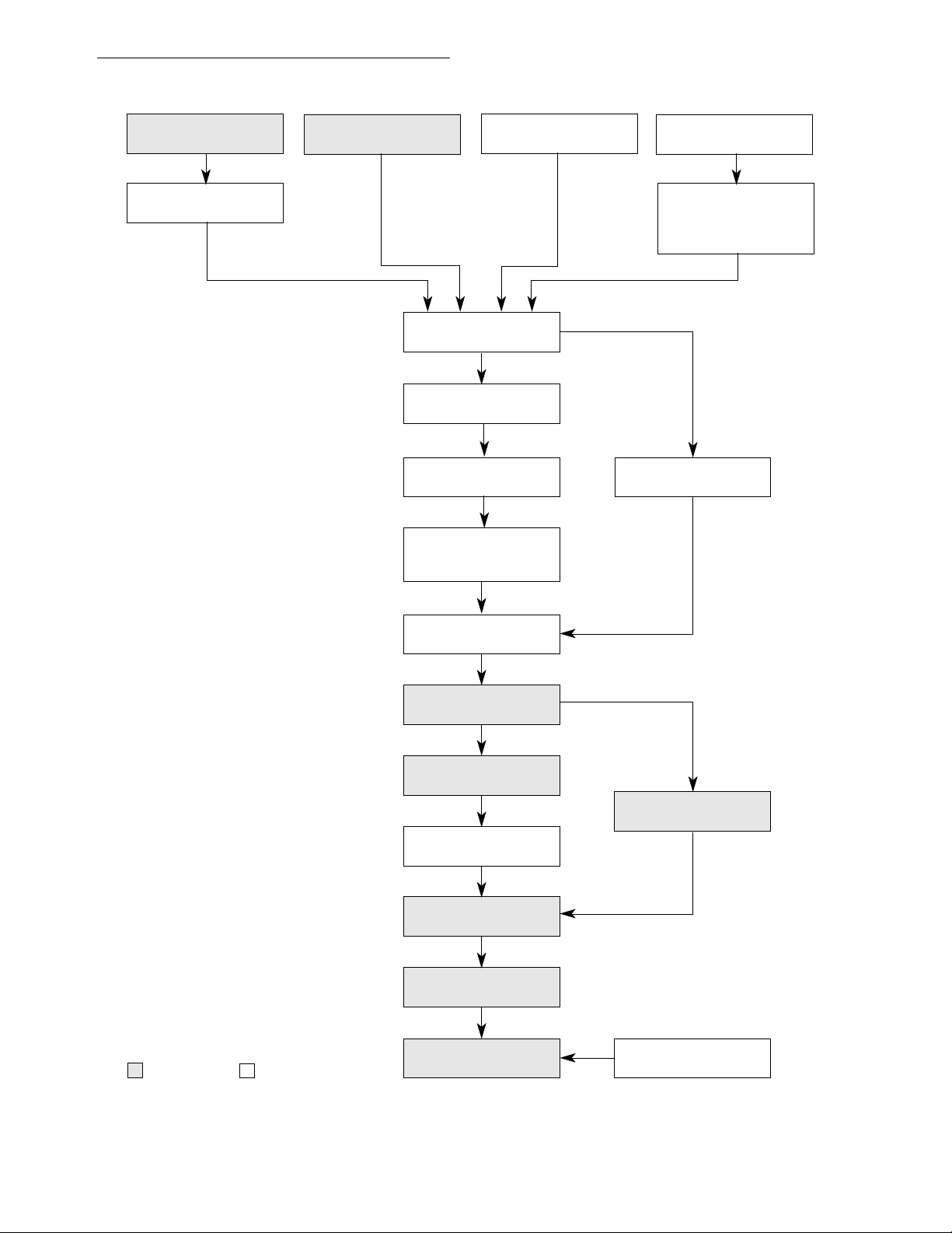
There are several steps that must be followed in order to create a FlexCore integrated microprocessor with an SCM68000. Figure 1-2 illustrates the standard cell design flow and the
tools required to complete each step. These steps include:
• Convert Design to Standard Cells Design—Begin by implementing the required system
functions with an SCM68000, peripherals, memory blocks, and cells from the Motorola
standard cell library.
• Capture Design on Workstation—Use the engineering workstation to capture the logic
schematic of cells and their interconnections.
• Logic Synthesis—The structural level description of the design is mapped to a more efficient structural description, which is accomplished by converting the Boolean equations for the design to a two-level sum of products representation and minimized.
• Generate Test Patterns—The stimulus and test patterns for the design are generated
for the functional simulation.
• Functional Simulation—Ensure that the logic of the schematic is functionally sound by
using Verilog, the encrypted C models and synthesis models provided by Motorola. No
timing information is yet associated with the simulations, and all propagation delays are
preset to 1 ns.
emiconduct
eescale S
Fr
• Calculate Node Delays— Motorola software (mdaDecal) calculates the estimated propagation delays of each node in the circuit. The design software estimates delays based
on the fanout, drive characteristics, and estimated interconnect capacitances of the
netlist and reveals potential timing problems.
• Path Delay Analysis—With path delay information from the Veritime software, the delays between the clocked elements of the circuit can be determined, and the critical
paths that limit the clock rate can be identified. Checking for setup, hold, and pulsewidth violations can also be accomplished.
• Perform Real-Time Simulation—The real-time simulation is run to verify full functionality
using the estimated propagation delays calculated by the design tools.
• Extract Test Vectors—The simulator records the input/output patterns generated during
the real-time simulation. The test vectors that Motorola will use to test the prototypes
are derived from these patterns.
• Automatic Place & Route—The circuit’s physical layout is created from the netlist using
automatic place and route software.
• Interconnect Analysis—After the cells are placed and routed, the interconnect capacitances are extracted. These capacitances replace those estimated earlier during the
calculation of the node delays.
• Re-Simulate—The circuit is re-simulated with Verilog to ensure no problems have arisen due to a change in load conditions. If changes have occurred or the simulation is different in any way, the test vectors must also be extracted again.
MOTOROLA
EC000 CORE PROCESSOR USER’S MANUAL
For More Information On This Product,
Go to: www.freescale.com
1-5
Page 19
Overview
Freescale Semiconductor, Inc.
nc...
, I
or
SYNTHESIS MODULES
LOGIC SYNTHESIS
(SYNOPSYS)
ENCRYPTED C
MODULES
GENERATE TEST PATTERNS
(STL/SYNOPSYS)
FUNCTIONAL SIMULATION
(VERILOG)
CALCULATE NODE DELAYS
(mdaDECAL)
PATH DELAY ANALYSIS
(VERITIME)
PERFORM REAL-TIME
SIMULATION
(VERILOG)
CONVERT DESIGN TO
STANDARD CELLS
CAPTURE DESIGN ON
WORKSTATION
(COMPOSER, VERILOG
HDL, VHDL)
PERFORM FAULT GRADING
(VERIFAULT)
emiconduct
eescale S
Fr
EXTRACT TEST VECTORS
(Summit Design)
AUTOMATIC PLACE & ROUTE
INTERCONNECT ANALYSIS
(mdaDECAL)
RE-SIMULATE
(VERILOG)
PATTERN, MASK AND
WAFER GENERATION
ASSEMBLY / TEST
NETLIST COMPARISON
(LVS)
1-6
MOTOROLA CUSTOMER
Figure 1-2. Standard Cell Design Flow
EC000 CORE PROCESSOR USER’S MANUAL
SHIP TESTED PROTOTYPES
For More Information On This Product,
Go to: www.freescale.com
FINAL TEST PROGRAM
MOTOROLA
Page 20
nc...
, I
or
emiconduct
eescale S
Fr
Freescale Semiconductor, Inc.
Overview
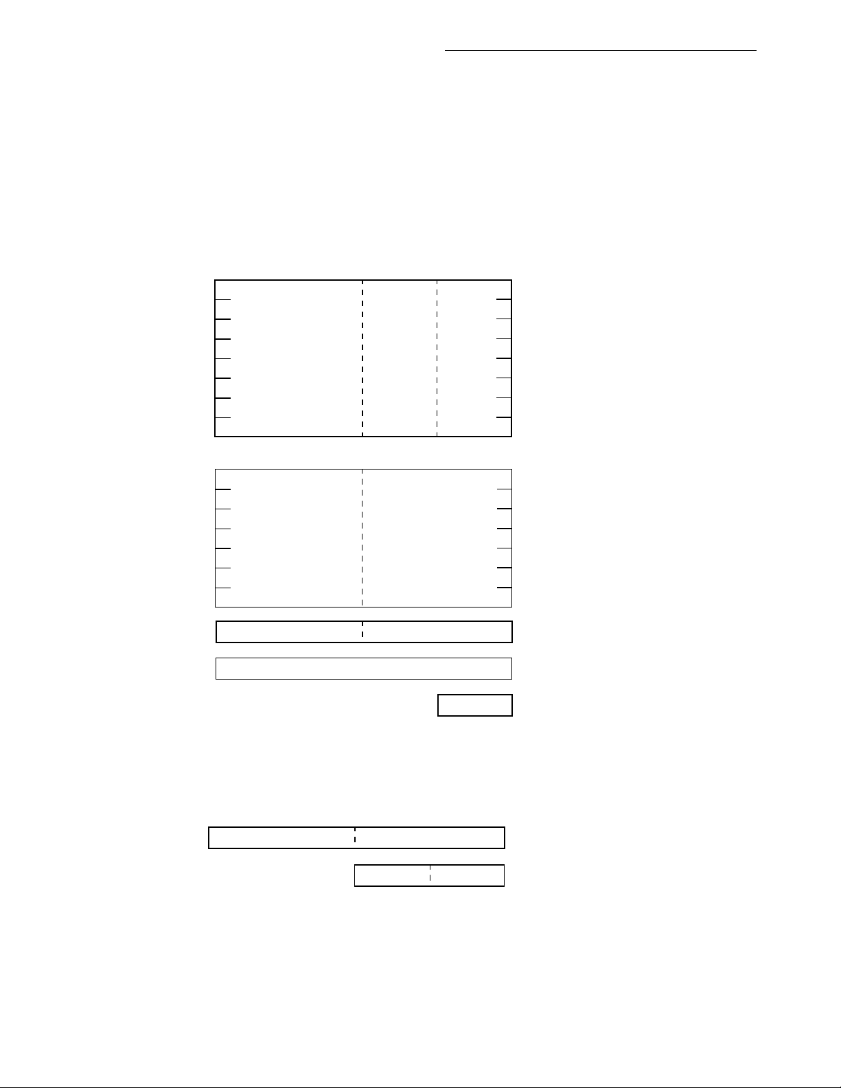
1.3 PROGRAMMING MODEL
The SCM68000 programming model is illustrated in Figure 1-3. It is separated into two
modes of access: user and supervisor. The user mode provides the execution environment
for the majority of application programs. The supervisor mode, which allows some additional
instructions and privileges, is used by the operating system and other system software.
Detailed information about the programming model can be found in the
grammer's Reference Manual
31 16 15 8 7 0
31 16 15
31
(M68000PM/AD).
(a) USER PROGRAMMING MODEL
D0
D1
D2
D3
EIGHT
DATA
D4
REGISTERS
D5
D6
D7
0
A0
A1
A2
SEVEN
A3
ADDRESS
REGISTERS
A4
A5
A6
A7
USER STACK
(USP) POINTER
0
70
PC
CCR
PROGRAM
COUNTER
CONDITION CODE
REGISTER
M68000 Family Pro-
MOTOROLA
31 16 15 0
15 8 7 0
CCR
(b) SUPERVISOR PROGRAMMING MODEL
Figure 1-3. Programming Model
EC000 CORE PROCESSOR USER’S MANUAL
For More Information On This Product,
Go to: www.freescale.com
A7'
SUPERVISOR STACK
(SSP)
POINTER
STATUS REGISTER
SR
1-7
Page 21
Overview
Freescale Semiconductor, Inc.
The user mode (see Figure 1-3(a)) provides access to 16 32-bit general-purpose registers
(D0–D7, A0–A7), a 32-bit program counter, and an 8-bit condition code register. The first
eight registers (D0–D7) are used as data registers for byte (8-bit), word (16-bit), and longword (32-bit) operations. The second set of seven registers (A0–A6) and the user stack
pointer (A7/USP) can be used as software stack pointers and base address registers. In
addition, the address registers can be used for word and long-word operations. All of the 16
registers can be used as index registers.
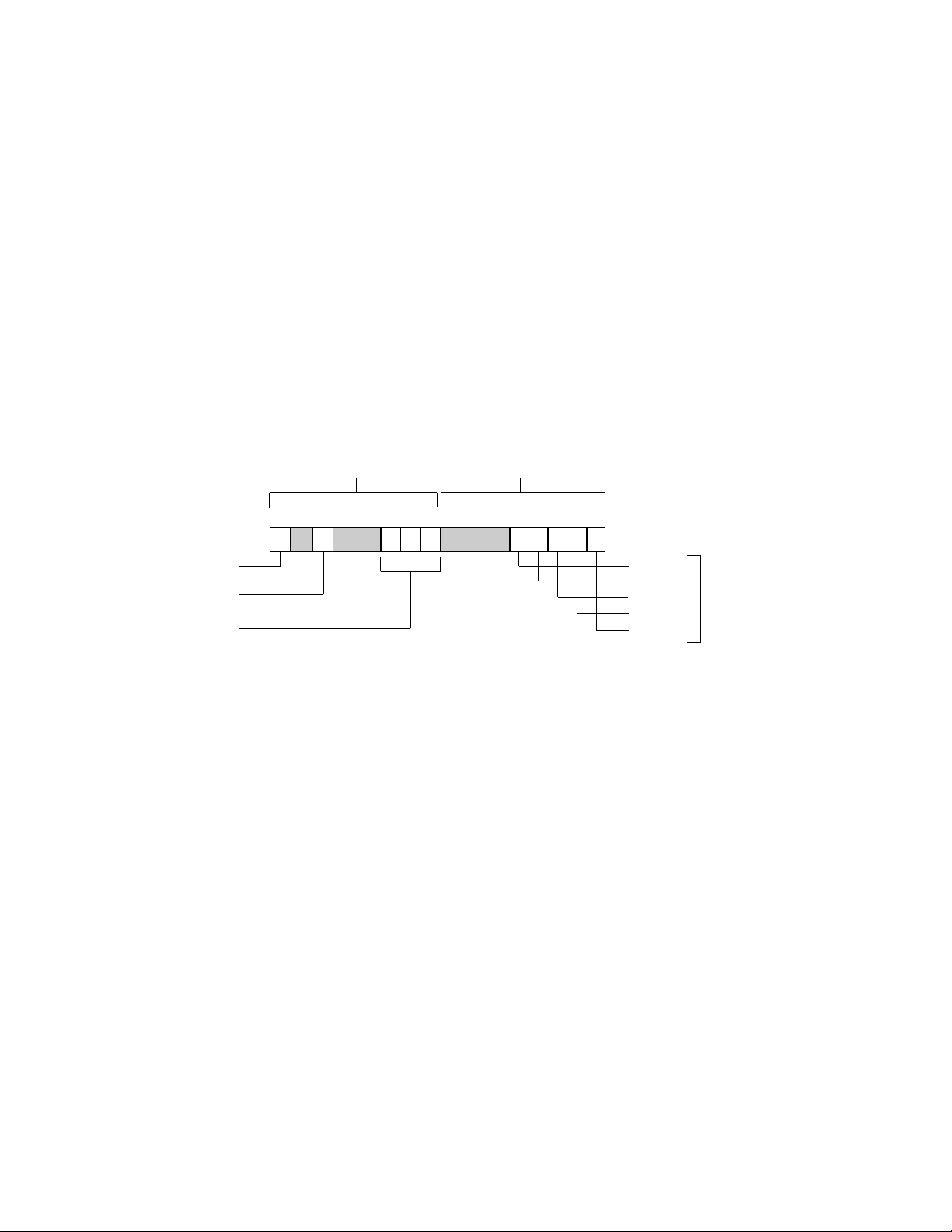
The supervisor mode (see Figure 1-3(b)) provides access to two supplementary registers,
the status register (high-order byte) and the supervisor stack pointer (A7'/SSP). The status
register (SR) (see Figure 1-4) contains the interrupt mask (eight levels available) and the
following condition codes: overflow (V), zero (Z), negative (N), carry (C), and extend (X).
Additional status bits indicate whether the SCM68000 is in the trace (T) mode and/or in the
supervisor (S) state. Bits 5, 6, 7, 11, 12, and 14 are undefined and reserved for future expansion.
nc...
, I
SYSTEM BYTE USER BYTE
or
emiconduct
eescale S
Fr
TRACE MODE
SUPERVISOR
STATE
INTERRUPT
MASK
15 13 10 8 4 0
S
T
III
210
XNZVC
Figure 1-4. Status Register
EXTEND
NEGATIVE
ZERO
OVERFLOW
CARRY
CONDITION
CODES
1-8
EC000 CORE PROCESSOR USER’S MANUAL
For More Information On This Product,
Go to: www.freescale.com
MOTOROLA
Page 22

Freescale Semiconductor, Inc.
Overview
1.4 DATA TYPES AND ADDRESSING MODES
Detailed information about the data types and addressing modes can be found in the
M68000 Family Programmer's Reference Manual
ports the five basic data types of the M68000 family:
1. Bit
2. Binary-Coded-Decimal (BCD) Digit (4 Bits)
3. Byte (8 Bits)
4. Word (16 Bits)
5. Long Word (32 Bits)
In addition, the instruction set supports operations on other data formats such as memory
addresses, status word, data, etc.
The SCM68000 also supports the basic addressing modes of the M68000 family. The register indirect addressing modes support postincrementing, predecrementing, offsetting, and
nc...
, I
indexing capabilities. The program counter relative mode also supports indexing and offsetting. Table 1-1 lists a summary of the data addressing modes for the SCM68000.
(M68000PM/AD). The SCM68000 sup-
or
emiconduct
eescale S
Fr
Table 1-1. Data Addressing Modes
Addressing Modes
Register Direct Addressing
Data Register Direct
Address Register Direct
Absolute Data Addressing
Absolute Short
Absolute Long
Program Counter Relative Addressing
Relative with Offset
Relative with Index and Offset
Register Indirect Addressing
Register Indirect
Postincrement Register Indirect
Predecrement Register Indirect
Register Indirect with Offset
Indexed Register Indirect with Offset
Immediate Data Addressing
Immediate
Quick Immediate
Implied Addressing
Implied Register
NOTES:
EA = Effective Address
Dn = Data Register
An = Address Register
( ) = Contents of
PC = Program Counter
d8= 8-Bit Offset (Displacement)
d
= 16-Bit Offset (Displacement)
16
N = 1 for byte, 2 for word, and 4 for long word. If An is the stack pointer and the
←
Xn = Address or Data Register Used as Index Register
SR = Status Register
USP = User Stack Pointer
SSP = Supervisor Stack Pointer
(xxx) = Absolute Address
operand size is byte, N = 2 to keep the stack pointer on a word boundary.
= Replaces
EA = Dn
EA = An
EA = (Next Word)
EA = (Next Two Words)
EA = (PC) + d
EA = (PC) + d8
EA = (An)
EA = (An), An ← An + N
An ← An – N, EA = (An)
EA = (An) + d
EA = (An) + (Xn) + d8
DATA = Next Word(s)
Inherent Data
EA = SR, USP, SSP, PC SR, USP, SSP, PC
Generation Syntax
Dn
An
(xxx).W
(xxx).L
16
16
(d16,PC)
(d8,PC,Xn)
(An)
(An)+
–(An)
(d16,An)
(d8,An,Xn)
#<data>
MOTOROLA
EC000 CORE PROCESSOR USER’S MANUAL
For More Information On This Product,
Go to: www.freescale.com
1-9
Page 23
Overview
Freescale Semiconductor, Inc.
1.5 DATA ORGANIZATION
The eight data registers support data operands of 1, 8, 16, or 32 bits. The seven address
registers and the active stack pointer support address operands of 32 bits.
1.5.1 Data Registers
Each data register is 32 bits wide. Byte operands occupy the low-order 8 bits, word operands, the low-order 16 bits, and long-word operands, the entire 32 bits. The least significant
bit is addressed as bit zero; the most significant bit is addressed as bit 31.
When a data register is used as either a source or a destination operand, only the appropriate low-order portion is changed; the remaining high-order portion is neither used nor
changed. For example, if 8 bits are to be moved into a data register, bits 0 through 7 will be
modified and bits 8 through 31 will not be changed.
1.5.2 Address Registers
nc...
, I
or
emiconduct
eescale S
Fr
Each address register (and the stack pointer) is 32 bits wide and holds a full 32-bit address.
Address registers do not support byte-sized operands. Therefore, when an address register
is used as a source operand, either the low-order word or the entire long-word operand is
used, depending upon the operation size. When an address register is used as the destination operand, the entire register is affected, regardless of the operation size. If the operation
size is word, operands are sign-extended to 32 bits before the operation is performed.
1.5.3 Data Organization In Memory
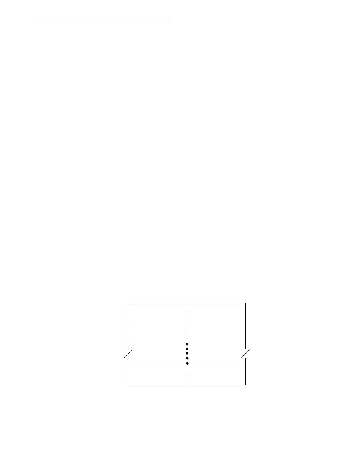
Bytes are individually addressable. As shown in Figure 1-5, the high-order byte of a word
has the same address as the word. The low-order byte has an odd address, one count
higher. Instructions and multibyte data are accessed only on word (even byte) boundaries.
If a long-word operand is located at address n (n even), then the second word of that operand is located at address n+2.
15 7 0141312111098 654321
ADDRESS
$000000
BYTE 000000 BYTE 000001
$000002
BYTE 000002 BYTE 000003
WORD 0
WORD 1
1-10
$FFFFFE
BYTE FFFFFE BYTE FFFFFF
WORD 7FFFFF
Figure 1-5. Word Organization in Memory
EC000 CORE PROCESSOR USER’S MANUAL
For More Information On This Product,
Go to: www.freescale.com
MOTOROLA
Page 24

Freescale Semiconductor, Inc.
The data types supported by the SCM68000 are bit data, integer data of 8, 16, and 32 bits,
32-bit addresses, and binary-coded-decimal data. Each data type is stored in memory as
shown in Figure 1-6.
Overview
1.6 INSTRUCTION SET SUMMARY
Table 1-2 lists the notational conventions used throughout this manual unless otherwise
specified. Table 1-3 lists the SCM68000 instruction set by opcode. In the syntax descriptions, the left operand is the source operand, and the right operand is the destination operand.
nc...
, I
or
emiconduct
eescale S
Fr
MOTOROLA
EC000 CORE PROCESSOR USER’S MANUAL
For More Information On This Product,
Go to: www.freescale.com
1-11
Page 25
Overview
Freescale Semiconductor, Inc.
nc...
, I
or
emiconduct
eescale S
Fr
BIT DATA:
INTEGER DATA:
MSB
n
n + 2
MSB
n
n + 2
n + 4
MSB
n
n + 2
n + 4
n + 6
n + 8
n + 10
ADDRESSES:
MSB
n
n + 2
n + 4
n + 6
n + 8
n + 10
MSB = MOST SIGNIFICANT BIT
LSB = LEAST SIGNIFICANT BIT
1 BYTE = 8 BITS
7
1 BYTE = 8 BITS
89101112131415
7
BYTE 0
BYTE 2 BYTE 3
LSB
1 WORD = 16 BITS
89101112131415
7
WORD 0
WORD 1
WORD 2
1 LONG WORD = 32 BITS
89101112131415
7
HIGH ORDER
LONG WORD 0
LOW ORDER
LONG WORD 1
LONG WORD 2
1 ADDRESS = 32 BITS
89101112131415
7
HIGH ORDER
ADDRESS 0
LOW ORDER
ADDRESS 1
ADDRESS 2
BYTE 1
LSB
LSB
LSB
0123456
0123456
n + 1
n + 3
0123456
0123456
0123456
1-12
DECIMAL DATA:
MSD LSD
MSD = MOST SIGNIFICANT DIGIT
LSD = LEAST SIGNIFICANT DIGIT
BCD 0 BCD 1
BCD 4 BCD 5
2 BINARY CODED DECIMAL DIGITS = 1 BYTE
Figure 1-6. Data Organization in Memory
EC000 CORE PROCESSOR USER’S MANUAL
For More Information On This Product,
Go to: www.freescale.com
89101112131415
7
BCD 2 BCD 3
BCD 6 BCD 7
0123456
MOTOROLA
Page 26

nc...
, I
or
emiconduct
eescale S
Fr
≠
×
÷
Λ
⊕
→
↔
Overview
Freescale Semiconductor, Inc.
Table 1-2. Notational Conventions
Single- and Double-Operand Operations
Not equal.
+ Arithmetic addition or postincrement indicator.
– Arithmetic subtraction or predecrement indicator.
Arithmetic multiplication.
Arithmetic division or conjunction symbol.
~ Invert; operand is logically complemented.
Logical AND
V Logical OR
Logical exclusive OR
Source operand is moved to destination operand.
Two operands are exchanged.
< Relational test; true if source operand is less than destination operand.
> Relational test; true if source operand is greater than destination operand.
<operand> Data used as an operand.
<operand> tested Operand is compared to zero and the condition codes are set appropriately.
<operand> sign-ex-
tended <operand>
<operand> shifted by
<count>
<operand> rotated by
<count>
bit number of <oper-
and>
TRAP
STOP Enter the stopped state, waiting for interrupts.
<operand>
If <condition>
then <operations>
else <operations>
#<xxx> or #<data>
10
An
Ax, Ay Source and destination address registers, respectively.
Dn Any Data Register n (example: D5 is data register 5)
Dx, Dy Source and destination data registers, respectively.
Rn Any Address or Data Register
Rx, Ry Any source and destination registers, respectively.
Xn Index Register—An, Dn, or suppressed.
<fmt>
( ) Identifies an indirect address in a register.
[ ] Identifies an indirect address in memory.
d
n
CCR
PC Program Counter
SR Status Register
All bits of the upper portion are made equal to the high-order bit of the lower portion.
The source operand is shifted by the number of count.
The source operand is rotated by the number of count.
Selects a single bit of the operand.
Other Operations
1 → S-bit of SR;
SSP – 4 → SSP; PC → (SSP); SSP – 2 → SSP;
SR → (SSP); Vector Address → PC
The operand is BCD; operations are performed in decimal.
Test the condition. If true, the operations after “then” are performed. If the condition is false and
the optional “else” clause is present, the operations after “else” are performed. If the condition
is false and "else" is omitted, the instruction performs no operation. Refer to the Bcc instruction
description as an example.
Register Specification
Any Address Register n (example: A3 is address register 3)
Data Format and Type
Operand Data Format: Byte (B), Word (W), Long (L)
Subfields and Qualifiers
Immediate data following the instruction word(s).
Displacement Value, n Bits Wide (example: d16 is a 16-bit displacement).
Register Names
Condition Code Register (lower byte of status register)
1-13
EC000 CORE PROCESSOR USER’S MANUAL
For More Information On This Product,
Go to: www.freescale.com
MOTOROLA
Page 27
nc...
, I
or
emiconduct
eescale S
Fr
Overview
Freescale Semiconductor, Inc.
Table 1-2. Notational Conventions (Continued)
Register Codes
C
cc Condition Codes from CCR
N Negative Bit in CCR
U Undefined, Reserved for Motorola Use
V Overflow Bit in CCR
X Extend Bit in CCR
Z Zero Bit in CCR
SP
SSP Supervisor (Master or Interrupt) Stack Pointer
USP User Stack Pointer
Í
<label> Assembly Program Label
<list> List of registers, for example D3–D0.
Carry Bit in CCR
Stack Pointers
Active Stack Pointer
Miscellaneous
Effective Address
Table 1-3. Instruction Set Summary
Opcode
ABCD
ADD Source + Destination → Destination
ADDA Source + Destination → Destination ADDA <ea>,An
ADDI Immediate Data + Destination → Destination ADDI # <data>,<ea>
ADDQ Immediate Data + Destination → Destination ADDQ # <data>,<ea>
ADDX Source + Destination + X → Destination
AND Source Λ Destination → Destination
ANDI Immediate Data Λ Destination → Destination ANDI # <data>, <ea>
ANDI to CCR Source Λ CCR → CCR ANDI # <data>, CCR
ANDI to SR
ASL, ASR Destination Shifted by <count> → Destination
Bcc
BCHG
BCLR
BKPT
BRA
BSET
BSR
BTST ~ (<bit number> of Destination) → Z;
CHK If Dn < 0 or Dn > Source then TRAP to CHK Instruction Vector CHK <ea>,Dn
CLR 0 → Destination CLR <ea>
CMP Destination – Source → cc CMP <ea>,Dn
Source10 + Destination10 + X → Destination
If supervisor state
then Source Λ SR → SR
else TRAP to Privilege Violation Trap
If (condition true) then PC + dn → PC
~ (<bit number> of Destination) → Z;
~ (<bit number> of Destination) → <bit number> of Destination
~ (<bit number> of Destination) → Z;
0 → <bit number> of Destination
Run breakpoint acknowledge cycle;
TRAP as illegal instruction
PC + dn → PC
~ (<bit number> of Destination) → Z;
1 → <bit number> of Destination
SP – 4 → SP; PC → (SP); PC + dn → PC
Operation Syntax
ABCD Dy,Dx
ABCD –(Ay), –(Ax)
ADD <ea>,Dn
ADD Dn,<ea>
ADDX Dy, Dx
ADDX –(Ay), –(Ax)
AND <ea>,Dn
AND Dn,<ea>
ANDI # <data>, SR
ASd Dx,Dy
ASd # <data>,Dy
ASd <ea>
Bcc <label>
BCHG Dn,<ea>
BCHG # <data>,<ea>
BCLR Dn,<ea>
BCLR # <data>,<ea>
BKPT # <data>
BRA <label>
BSET Dn,<ea>
BSET # <data>,<ea>
BSR <label>
BTST Dn,<ea>
BTST # <data>,<ea>
1-14
EC000 CORE PROCESSOR USER’S MANUAL
For More Information On This Product,
Go to: www.freescale.com
MOTOROLA
Page 28

nc...
, I
or
emiconduct
eescale S
Fr
Overview
Freescale Semiconductor, Inc.
Table 1-3. Instruction Set Summary (Continued)
CMPA Destination – Source → cc CMPA <ea>,An
CMPI Destination – Immediate Data → cc CMPI # <data>,<ea>
CMPM Destination – Source → cc CMPM (Ay)+, (Ax)+
DBcc
DIVS Destination ÷ Source → Destination DIVS.W <ea>,Dn32/16 → 16r:16q
DIVU Destination ÷ Source → Destination DIVU.W <ea>,Dn32/16 → 16r:16q
EOR Source ⊕ Destination → Destination EOR Dn,<ea>
EORI Immediate Data ⊕ Destination → Destination EORI # <data>,<ea>
EORI to CCR Source ⊕ CCR → CCR EORI # <data>,CCR
EORI to SR
EXG Rx ↔ Ry
EXT Destination Sign-Extended → Destination
ILLEGAL
JMP Destination Address → PC JMP <ea>
JSR
LEA <ea> → An LEA <ea>,An
LINK
LSL,LSR Destination Shifted by <count> → Destination
MOVE Source → Destination MOVE <ea>,<ea>
MOVEA Source → Destination MOVEA <ea>,An
MOVE to
CCR
MOVE from
SR
MOVE to SR
MOVE USP
MOVEM
MOVEP Source → Destination
MOVEQ Immediate Data → Destination MOVEQ # <data>,Dn
MULS Source × Destination → Destination MULS.W <ea>,Dn16 x 16 → 32
MULU Source × Destination → Destination MULU.W <ea>,Dn16 x 16 → 32
NBCD
NEG 0 – (Destination) → Destination NEG <ea>
NEGX 0 – (Destination) – X → Destination NEGX <ea>
NOP None NOP
NOT ~Destination → Destination NOT <ea>
OR Source V Destination → Destination
If condition false then (Dn – 1 → Dn;
If Dn ≠ –1 then PC + dn → PC)
If supervisor state
then Source ⊕SR → SR
else TRAP to Privilege Violation Trap
SSP – 4 → SSP; PC → (SSP);
SSP – 2 → SSP; SR → (SSP);
Illegal Instruction Vector Address → PC
SP – 4 → SP; PC → (SP)
Destination Address → PC
SP – 4 → SP; An → (SP)
SP → An, SP + dn → SP
Source → CCR MOVE <ea>,CCR
SR → Destination MOVE SR,<ea>
If supervisor state
then Source → SR
else TRAP to Privilege Violation Trap
If supervisor state
then USP → An or An → USP
else TRAP to Privilege Violation Trap
Registers → Destination;
Source → Registers
0 – (Destination10) – X → Destination
DBcc Dn,<label>
EORI # <data>,SR
EXG Dx,Dy
EXG Ax,Ay
EXG Dx,Ay
EXG Ay,Dx
EXT.W Dnextend byte to word
EXT.L Dnextend word to long word
ILLEGAL
JSR <ea>
LINK An, # <displacement>
LSd Dx,Dy
LSd # <data>,Dy
LSd Í
MOVE <ea>,SR
MOVE USP,An
MOVE An,USP
MOVEM <list>,<ea>
MOVEM <ea>,<list>
MOVEP Dx,(d16,Ay)
MOVEP (d16,Ay),Dx
NBCD <ea>
OR <ea>,Dn
OR Dn,<ea>
1-15 EC000 CORE PROCESSOR USER’S MANUAL MOTOROLA
For More Information On This Product,
Go to: www.freescale.com
Page 29

nc...
, I
or
emiconduct
eescale S
Fr
Overview
Freescale Semiconductor, Inc.
Table 1-3. Instruction Set Summary (Continued)
ORI Immediate Data V Destination → Destination ORI # <data>,<ea>
ORI to CCR Source V CCR → CCR ORI # <data>,CCR
ORI to SR
PEA Sp – 4 → SP; <ea> → (SP) PEA <ea>
RESET
ROL, ROR Destination Rotated by <count> → Destination
ROXL,
ROXR
RTE
RTR
RTS (SP) → PC; SP + 4 → SP RTS
SBCD
Scc
STOP
SUB Destination – Source → Destination
SUBA Destination – Source → Destination SUBA <ea>,An
SUBI Destination – Immediate Data → Destination SUBI # <data>,<ea>
SUBQ Destination – Immediate Data → Destination SUBQ # <data>,<ea>
SUBX Destination – Source – X → Destination
SWAP Register [31:16] ↔ Register [15:0] SWAP Dn
TAS
TRAP
TRAPV If V then TRAP to TRAPV Instruciton Vector TRAPV
TST Destination Tested → Condition Codes TST <ea>
UNLK An → SP; (SP) → An; SP + 4 → SP UNLK An
NOTE: d is direction, L or R.
If supervisor state
else TRAP to Privilege Violation Trap
If supervisor state
else TRAP to Privilege Violation Trap
Destination Rotated with X by <count> → Destination
If supervisor state
else TRAP to Privilege Violation Trap
(SP) → CCR; SP + 2 → SP;
(SP) → PC; SP + 4 → SP
Destination
If condition true
else 0s → Destination
If supervisor state
else TRAP to Privilege Violation Trap
Destination Tested → Condition Codes; 1 → bit 7 of
1 → S-bit of SR;
SSP – 4 → SSP; PC → (SSP); SSP – 2 → SSP;
SR → (SSP); Vector Address → PC
then Source V SR → SR
then Assert RESETOB Line
then (SP) → SR; SP + 2 → SP; (SP) → PC;
SP + 4 → SP;
restore state and deallocate stack according to (SP)
– Source
10
then 1s → Destination
then Immediate Data → SR; STOP
Destination
– X → Destination
10
ORI # <data>,SR
RESET
ROd Dx,Dy
ROd # <data>,Dy
ROd Í
ROXd Dx,Dy
ROXd # <data>,Dy
ROXd Í
RTE
RTR
SBCD Dx,Dy
SBCD –(Ax),–(Ay)
Scc <ea>
STOP # <data>
SUB <ea>,Dn
SUB Dn,<ea>
SUBX Dx,Dy
SUBX –(Ax),–(Ay)
TAS <ea>
TRAP # <vector>
1-16 EC000 CORE PROCESSOR USER’S MANUAL MOTOROLA
For More Information On This Product,
Go to: www.freescale.com
Page 30

Freescale Semiconductor, Inc.
SECTION 2
SIGNAL DESCRIPTION
nc...
, I
or
emiconduct
This section contains descriptions of the SCM68000 (EC000 core)
The input and output signals are shown in Figure 2-1. Table 2-1 lists the pins, signal names,
type, and whether they are three-stateable. The following paragraphs provide brief descriptions of the signals and references (where applicable) to other paragraphs that contain more
information about the signals.
NOTE
The terms
manual to avoid confusion when describing a mixture of "activelow" and "active-high" signals. The term
used to indicate that a signal is active or true, independently of
whether that level is represented by a high or low voltage. The
negate
term
tive or false.
assertion
or
negation
and
negation
is used to indicate that a signal is inac-
are used extensively in this
assert
1
input and output signals.
or
assertion
is
2.1 ADDRESS BUS (A31–A0)
This 32-bit, unidirectional, three-state bus is capable of addressing 4 Gbytes of address
space. This bus provides the address for bus operation during all cycles except interrupt
acknowledge cycles. During interrupt acknowledge cycles, address lines A1, A2, and A3
provide the level number of the interrupt being acknowledged, and address lines A31–A4
and A0 are driven to a logic high.
eescale S
Fr
2.2 DATA BUS (D15–D0)
This 16-bit, bidirectional, three-state bus is the general-purpose data-path. The data bus
transfers and accepts data in either word or byte length if the SCM68000 is operating in the
16-bit mode. If the SCM68000 is operating in the 8-bit mode, it drives the entire bus during
writes, but only the lower eight bits (D7–D0) contain valid data. In the 8-bit mode, the
SCM68000 ignores the data on data lines D15–D8 during read cycles. During an interrupt
acknowledge cycle, the external device supplies the vector number on data lines D7–D0.
2.3 CLOCK (CLKI, CLKO)
The CLKI input is internally buffered for development of the internal clocks needed by the
SCM68000. This clock signal is a constant-frequency square wave that requires no stretching or shaping. The clock signal must conform to minimum and maximum pulse-width times
1.
The SCM68000 is the name of the Verilog model for the EC000 core. The remainder of this section will
refer to the EC000 core as only the SCM68000.
MOTOROLA
EC000 CORE PROCESSOR USER’S MANUAL
For More Information On This Product,
Go to: www.freescale.com
2-1
Page 31

Signal Description
Freescale Semiconductor, Inc.
nc...
, I
or
RESETIB
HALTIB
CLKI
BRB
BGACKB
DTACKB
BERRB
MODE
AVECB
IPLB2–IPLB0
SCM68000
RESETOB
HALTOB
CLKO
BGB
ASB
UDSB
LDSB
DSB
RMCB
COEB
RWB
ERWB
SIZ1–SIZ0
FC2–FC0
A31–A0
AOEB
D15–D0
DOEB
TESTCLK
IPENDB
emiconduct
eescale S
Fr
TSCAE
TEST
DISB
REFILLB
STOP
STATUSB
Figure 2-1. Input/Output Signals
Table 2-1. Signal Summary
Hi-Z on
Signal Name
Address Bus
Address Output Enable AOEB Output Low STD No No
Address Strobe ASB Output Low TS No Yes
Autovector AVECB Input Low STD N/A N/A
Bus Error BERRB Input Low STD N/A N/A
Bus Grant BGB Output Low STD No No
Bus Grant Acknowledge BGACKB Input Low STD N/A N/A
Bus Request BRB Input Low STD N/A N/A
Clock In CLKI Input High STD N/A N/A
Clock Out CLKO Output High STD No No
Control Output Enable COEB Output Low STD No No
Data Bus D15–D0 Input/Output High TS Yes Yes
Disable Control DISB Input Low STD N/A N/A
Data Output Enable DOEB Output Low STD No No
Mnemonic Input/ Output
A31–A0 Output High TS No Yes
Active
State
Output
Circuit
HALTIB or
STOP
Instruction
Hi-Z on Bus
Relinquish
or RESETIB
2-2
EC000 CORE PROCESSOR USER’S MANUAL
For More Information On This Product,
Go to: www.freescale.com
MOTOROLA
Page 32

nc...
, I
or
emiconduct
Freescale Semiconductor, Inc.
Signal Description
Table 2-1. Signal Summary
Hi-Z on
Signal Name
Data Strobe
Data Transfer Acknowledge DTACKB Input Low STD N/A N/A
Early Read Write ERWB Output Low TS No Yes
Function Code FC2–FC0 Output High TS No Yes
Halt In HALTIB Input Low STD N/A N/A
Halt Out HALTOB Output Low STD No No
Interrupt Pending IPENDB Output Low STD No No
Interrupt Control IPLB2–IPLB0 Input Low STD N/A N/A
Lower Data Strobe LDSB Output Low TS No Yes
Mode MODE Input High STD N/A N/A
CPU Pipe Refill REFILLB Output Low STD No No
Reset In RESETIB Input Low STD N/A N/A
Reset Out RESETOB Output Low STD No No
Read-Modify-Write RMCB Output Low TS No Yes
Read/Write RWB Output Low TS No Yes
Data Transfer Size SIZ1, SIZ0 Output High TS No Yes
Microsequencer Status Indication STATUSB Output Low STD No No
Stop STOP Output High STD No No
Test TEST Input High STD N/A N/A
Test Clock TESTCLK Output High STD No No
Address Three-State Control TSCAE Output High STD No No
Upper Data Strobe UDSB Output Low TS No Yes
NOTE: TS = Three-State Output
STD = Standard CMOS Output
Mnemonic Input/ Output
DSB Output Low TS No Yes
Active
State
Output
Circuit
HALTIB or
STOP
Instruction
Hi-Z on Bus
Relinquish
or RESETIB
listed in the Section 7 Electrical Characteristics . The CLKO output follows CLKI to provide
a reference for testing.
2.4 ASYNCHRONOUS BUS CONTROL
eescale S
Fr
The following signals control asynchronous data transfers: address strobe, read/write, early
read/write, data strobe, upper data strobe, lower data strobe, read-modify-write, data transfer size, and data transfer acknowledge. These signals are described in the following paragraphs.
2.4.1 Address Strobe (ASB)
This active low, three-state signal indicates that the information on the address bus is a valid
address.
2.4.2 Read/Write (RWB) and Early Read/Write (ERWB)
The active-low, three-state RWB output signal defines the data bus transfer as a read or
write cycle. The active-low, three-state ERWB output signal indicates a write cycle one-half
clock cycle earlier than the read/write signal. Negation times are the same for both signals.
These signals relate to the data strobe signals described in the following paragraphs.
MOTOROLA
EC000 CORE PROCESSOR USER’S MANUAL
For More Information On This Product,
Go to: www.freescale.com
2-3
Page 33

Signal Description
Freescale Semiconductor, Inc.
2.4.3 Upper and Lower Data Strobes (UDSB, LDSB), and Data Strobe
(DSB)
These active-low, three-state signals and RWB control the flow of data on the data bus.
Table 2-2 lists the combinations of these signals and the corresponding data on the bus.
When the RWB line is a logic high, the SCM68000 reads from the data bus. When the RWB
line is a logic low, the SCM68000 writes to the data bus. In the case of an 8-bit write in 16bit mode, the same data will be on both D7–D0 and D15–D8.
Table 2-2. Upper and Lower Data Strobe Control of Data Bus
UDSB
High
Low Low High Valid Data Bits 15–8 Valid Data Bits 7–0
High Low High No Valid Data Valid Data Bits 7–0
Low High High Valid Data Bits 15–8 No Valid Data
Low Low Low Valid Data Bits 15-8 Valid Data Bits 7–0
High Low Low Valid Data Bits 7–0 Valid Data Bits 7–0
nc...
Low High Low Valid Data Bits 15–8 Valid Data Bits 15–8
LDSB RWB D15–D8 D7–D0
High — No Valid Data No Valid Data
, I
or
emiconduct
eescale S
Fr
In 8-bit mode, UDSB is always forced high and only the LDSB signal and RWB are used to
control the flow of data on the data bus. Table 2-3 lists the combinations of these signals
and the corresponding data on the bus. When the RWB line is a logic high, the SCM68000
reads from the data bus. When the RWB line is a logic low, the SCM68000 drives the data
bus.
Table 2-3. Lower Data Strobe Control of Data Bus
LDSB
High
Low High Read Cycle
Low Low Write Cycle
RWB Data Bus Operation
— No Valid Data
DSB is an active-low, three-state output signal that is asserted whenever LDSB or UDSB is
asserted.
2.4.4 Data Transfer Acknowledge (DTACKB)
This active-low input indicates the completion of the data transfer. When the SCM68000 recognizes DTACKB during a read cycle, data is latched and the bus cycle is terminated. When
DTACKB is recognized during a write cycle, the data bus enters a high-impedance state and
the bus cycle is terminated.
2.4.5 Data Transfer Size (SIZ1–SIZ0)
These active-high, three-state output signals provide information on the size of the operand
transfer. These outputs indicate the number of bytes to be transferred in the current bus
cycle. Table 2-4 indicates the size signal encoding.
2-4
EC000 CORE PROCESSOR USER’S MANUAL
For More Information On This Product,
Go to: www.freescale.com
MOTOROLA
Page 34

nc...
, I
or
Freescale Semiconductor, Inc.
Table 2-4. Data Transfer Size
SIZ1 SIZ0 Size
1
0 1 Word
Size Code Output
0 Byte
Signal Description
2.4.6 Read-Modify-Write (RMCB)
This active-low, three-state output line is logic low during read-modify-write cycles and indicates an indivisible bus sequence. This is described in
3.1.3 Read-Modify-Write Cycle .
2.5 BUS ARBITRATION CONTROL
The bus request, bus grant, and bus grant acknowledge signals form the bus arbitration control signals that determine which device will be the bus master device. There are two possible arbitration protocols: 2-wire and 3-wire. In the 2-wire protocol, BGACKB is not used and
must be negated.
2.5.1 Bus Request (BRB)
This active-low input is the combination of bus request signals from all other devices that
could be bus masters. This signal indicates to the SCM68000 that some other device needs
to become the bus master. Bus requests can be issued at any time during a cycle or
between cycles.
emiconduct
eescale S
Fr
2.5.2 Bus Grant (BGB)
This active-low output indicates to all other potential bus master devices that the SCM68000
will relinquish bus control at the end of the current bus cycle.
2.5.3 Bus Grant Acknowledge (BGACKB)—3-Wire Protocol Only
This active-low input indicates that some other device has become the bus master. This signal should not be asserted until the following four conditions are met:
1. A bus grant has been received.
2. Address strobe is negated, which indicates that the SCM68000 is not using the bus.
3. Data transfer acknowledge is negated, which indicates that neither memory nor peripherals are using the bus.
4. Bus grant acknowledge is negated, which indicates that no other device is still claiming
to be the bus master.
2.6 INTERRUPT CONTROL (IPLB2–IPLB0)
These active-low input signals indicate the encoded priority level of the device requesting
an interrupt. Level 7, which cannot be masked, has the highest priority; level 0 indicates that
no interrupts have been requested. IPLB0 is the least significant bit of the encoded level,
and IPLB2 is the most significant bit. For each interrupt request, these signals must maintain
the interrupt request level until the SCM68000 acknowledges the interrupt to guarantee that
MOTOROLA
EC000 CORE PROCESSOR USER’S MANUAL
For More Information On This Product,
Go to: www.freescale.com
2-5
Page 35

Signal Description
Freescale Semiconductor, Inc.
the interrupt is recognized. Table 2-5 lists the interrupt levels, the states of IPLB2–IPLB0 that
define each level, and the mask value that allows an interrupt at each level.
Table 2-5. Interrupt Levels and Mask Values
Requested
Interrupt Level
0
1 High High Low 0
2 High Low High 1–0
3 High Low Low 2–0
4 Low High High 3–0
5 Low High Low 4–0
6 Low Low High 5–0
7 Low Low Low 7–0
Control Line Status
IPLB2 IPLB1 IPLB0
High High High No Interrupt Is Requested
Interrupt Mask Level
Required for Recognition
2.7 SYSTEM CONTROL
nc...
, I
or
emiconduct
eescale S
Fr
The system control inputs are used to reset, halt, disable, and test the SCM68000 as well
as signal a bus error to the SCM68000 and choose either the 8-bit or 16-bit mode. The two
outputs reset the external devices in the system and signal to those devices when the
SCM68000 has stopped executing instructions because of an error. The system control signals are described in the following paragraphs.
2.7.1 Bus Error (BERRB)
This input signal indicates a problem in the current bus cycle. The problem may be the following:
1. No response from a device.
2. No interrupt vector number returned.
3. An illegal access request rejected by a memory management unit.
4. Some other application-dependent error.
The SCM68000 either retries the bus cycle or performs exception processing, as determined by interaction between the bus error signal and the halt signal.
2.7.2 Reset External/Internal (RESETIB, RESETOB)
The assertion of the active-low input, RESETIB can start a system initialization sequence by
resetting the SCM68000. The SCM68000 assertion of RESETOB (from executing a RESET
instruction) resets all external devices of a system without affecting the internal state of the
SCM68000. The interaction of RESETIB, RESETOB, and HALTIB is described in
Reset
.
4.3.1
2.7.3 Halt External/Internal (HALTIB, HALTOB)
Asserting the active-low input, HALTIB causes the SCM68000 to stop bus activity at the
completion of the current bus cycle. This operation places all control signals in the inactive
state and places the data bus in a high-impedance state (see Table 2-1).
2-6
EC000 CORE PROCESSOR USER’S MANUAL
For More Information On This Product,
Go to: www.freescale.com
MOTOROLA
Page 36

Freescale Semiconductor, Inc.
When the SCM68000 has stopped executing instructions (in the case of a double bus fault
condition, for example), the active-low output, HALTOB, is asserted by the SCM68000 to
indicate the condition to external devices.
Signal Description
2.7.4 Mode (MODE)
This input selects between the 8-bit and 16-bit operating modes. If this input is grounded
during reset, the SCM68000 comes out of reset in the 8-bit mode. If this input is tied to a
logic high during reset, the SCM68000 comes out of reset in the 16-bit mode. Changing this
input during normal operation may produce unpredictable results.
2.7.5 Disable Control (DISB)
This active-low signal is designed to place the SCM68000 into a quiescent state allowing
other sections of the circuit to be tested without interference from the SCM68000. When this
signal is asserted, the SCM68000 responds with the following with minimum gate delay if
the clock is stopped:
nc...
, I
or
emiconduct
eescale S
Fr
• All three-state outputs will be placed into a high-impedance state.
• The bus grant (BGB), clock output (CLKO), halt output (HALTOB), reset output (RESE-
TOB), microsequencer status (STATUSB), stop instruction indicator (STOP), and test
clock (TESTCLK) signals remain at the state they were in when the clock was stopped.
• The remaining outputs are disabled, forcing them into an inactive state.
If the clock is running, the SCM68000 responds with the following with minimum gate delay:
• All three-state outputs will be placed into a high-impedance state.
• The clock output (CLKO) continues to follow the clock input (CLKI).
• The microsequencer status (STATUSB) signal is forced to a logic low.
• The test clock (TESTCLK) signal is forced to a logic low.
• The remaining outputs are disabled, forcing them into their inactive states.
When DISB is asserted, it is internally gated with the internal SCM68000 reset and halt
signals after the input synchronizer. The user must ensure that the system is reset as discussed in
4.3.1 Reset .
2.7.6 Test Mode (TEST)
This active-high input signal allows the SCM68000 to enter the test mode. This permits
application of standard M68000 family test mode patterns to the SCM68000.
2.7.7 Test Clock (TESTCLK)
If the SCM680000 is properly reset during simulation, the TESTCLK signal will begin to
pulse. A single period of the test clock consists of ten SCM68000 clock periods (six clocks
low, four clocks high). This signal is generated by an internal ring counter that may come up
in any state. (At power-on, it is impossible to guarantee phase relationship of TESTCLK to
CLKI.) The TESTCLK signal is a free-running clock that runs regardless of the state of the
MPU bus. For more information on resetting the SCM68000 for simulation, see
tializing the SCM68000 for Simulation
MOTOROLA
EC000 CORE PROCESSOR USER’S MANUAL
For More Information On This Product,
Go to: www.freescale.com
.
4.3.1.2 Ini-
2-7
Page 37

nc...
, I
or
Signal Description
Freescale Semiconductor, Inc.
2.7.8 Autovector (AVECB)
This active-low input signal indicates that the SCM68000 should use automatic vectoring for
an interrupt during an interrupt acknowledge cycle. AVECB should be asserted only during
an interrupt acknowledge cycle or erratic controller operation may occur.
2.8 THREE-STATE CONTROL
The following signals are the enable signals to put SCM68000 signals into a high-impedence
state.
2.8.1 Address Output Enable (AOEB)
This active-low output signal is negated to put the address lines (A31–A0), function codes
(FC2–FC0), size codes (SIZ1–SIZ0), early read/write (ERWB), and read/write (RWB) into a
high-impedance state.
2.8.2 Control Output Enable (COEB)
This active-low output signal is negated to put the address strobe (ASB), data strobe (DSB),
lower data strobe (LDSB), read-modify-write (RMCB), and upper data strobe (UDSB) into a
high-impedance state.
emiconduct
eescale S
Fr
2.8.3 Data Output Enable (DOEB)
This active-low output signal is negated to put the data lines of the SCM68000 into a highimpedance state.
2.9 PROCESSOR STATUS
These signals are used to indicate pending interrupts and when the SCM68000 is between
bus cycles or at instruction boundaries. They also show when the instruction pipe is refilling
and when the processor has been stopped. The signals are described in the following paragraphs.
2.9.1 Function Codes (FC2–FC0)
These active-high, three-state function code outputs indicate the mode (user or supervisor)
and the address space currently being accessed as listed in Table 2-6. The function code
outputs are valid whenever ASB is active.
Table 2-6. Function Code Outputs
Function Code Output
FC2 FC1 FC0
Low Low Low (Undefined, Reserved)
Low Low High User Data
Low High Low User Program
Low High High (Undefined, Reserved)
High Low Low (Undefined, Reserved)
High Low High Supervisor Data
High High Low Supervisor Program
High High High Interrupt Acknowledge
Cycle Time
2-8
EC000 CORE PROCESSOR USER’S MANUAL
For More Information On This Product,
Go to: www.freescale.com
MOTOROLA
Page 38

Freescale Semiconductor, Inc.
Signal Description
2.9.2 Address Three-State Control (TSCAE)
This active-high output signal is asserted between bus cycle accesses of the SCM68000.
2.9.3 Stop Instruction Indicator (STOP)
This output line pulses at one fourth the rate of the CLKI signal with an active time of one
clock period when the STOP instruction is executed.
2.9.4 Interrupt Pending (IPENDB)
This active-low output signal indicates a valid interrupt has been recognized.
2.9.5 CPU Pipe Refill (REFILLB)
This active-low output signal is asserted for one clock period to indicate that a refill of the
CPU pipe is occurring due to a change in program flow. This is used for emulator support.
nc...
, I
or
emiconduct
eescale S
Fr
2.9.6 Microsequencer Status Indication (STATUSB)
This active-low output signal indicates microsequencer status and is used for emulator support. The number of clock cycles for which this signal is asserted indicates the status of the
SCM68000. When the SCM68000 approaches an instruction boundary, this signal is normally asserted for one clock cycle. Table 2-7 indicates exceptions that are indicated by the
assertion of this signal for more than one cycle.
Table 2-7. Status Indication Exceptions
Asserted For
One Clock Sequencer at instruction boundary - will begin execution of next instruction
Sequencer at instruction boundary - will not begin the next instruction immediately due to:
• Pending Interrupt Exception or
Two Clocks
Three Clocks
Continuously
• Pending Trace Exception or
• Illegal Instruction Exception or
• Pending Breakpoint Instruction Exception or
• Privileged Instruction Exception
Exception processing to begin for:
• Bus Error or
• Address Error or
• A-line Instruction or
• Spurious Interrupt or
• Illegal Instruction or
• Privileged Instruction or
• Auto vectored Interrupt or
• F-line Instruction
Core is:
• Halted
• Reset
Indicates
2.10 MULTIPLEXING PINS
When a design is implemented, certain pins need to be multiplexed to the pads for testing
purposes. Motorola recommends that all the pins on the SCM68000 be multiplexed to offer
a means for testing the processor with test vectors provided by Motorola. This will provide
maximum fault coverage. Varying degrees of fault coverage can be obtained depending on
which pins the user does or does not multiplex.
MOTOROLA
EC000 CORE PROCESSOR USER’S MANUAL
For More Information On This Product,
Go to: www.freescale.com
2-9
Page 39

nc...
, I
or
emiconduct
eescale S
Fr
Signal Description
Freescale Semiconductor, Inc.
All pins must be multiplexed according to the requirements in Table 2-8. However, it is necessary that the proper three-state control signal be used to control the three-state drivers as
stated in
2.8 Three-State Control . Table 2-8 shows a list of pins and the priority with which
they need to be multiplexed. The priority column has three possible responses: required,
required if used, not required, and internal. The “required if used” response means that the
pin must be muxed out if the pin is used in the current design. The "internal" response means
that the signal may be used internally and must not be muxed out.
Table 2-8. Pin Multiplexing Priority
Signal Name
Address Bus
Address Bus A23–A0 Output Required
Address Output Enable AOEB Output Internal
Address Strobe ASB Output Required
Bus Error BERRB Input Required
Bus Grant BGB Output Required
Bus Grant Acknowledge BGACKB Input Required
Bus Request BRB Input Required
Clock In CLKI Input Required
Clock Out CLKO Output Required If Used
Control Output Enable COEB Output Internal
Data Bus D15–D0 Input/Output Required
Disable Control DISB Input Internal
Data Output Enable DOEB Output Internal
Data Strobe DSB Output Required If Used
Data Transfer Acknowledge DTACKB Input Required
Test Clock TESTCLK Output Not Required
Early Read Write ERWB Output Required If Used
Function Code FC2–FC0 Output Required
Halt In* HALTIB Input Required
Halt Out* HALTOB Output Required
Interrupt Pending IPENDB Output Required If Used
Interrupt Control IPLB2–IPLB0 Input Required
Lower Data Strobe LDSB Output Required
Mode MODE Input Required
CPU Pipe Refill REFILLB Output Required If Used
Reset In* RESETIB Input Required
Reset Out* RESETOB Output Required
Read-Modify-Write RMCB Output Required If Used
Read/Write RWB Output Required
Data Transfer Size SIZ1, SIZ0 Output Required If Used
Microsequencer Status Indication STATUSB Output Required If Used
Stop STOP Output Required If Used
Test TEST Input Required
Address Three-State Control TSCAE Output Required If Used
Upper Data Strobe UDSB Output Required
Autovector AVECB Input Required
* HALTIB and HALTOB may share a single pin, HALTB, that is functionally equivalent to
the circuit in Figure 4-10.
RESETIB and RESETOB may share a single pin, RESETB, that is functionally
equivalent to the circuit in Figure 4-10.
Pin Name Input/Output Priority
A31–A24 Output Required If Used
2-10
EC000 CORE PROCESSOR USER’S MANUAL
For More Information On This Product,
Go to: www.freescale.com
MOTOROLA
Page 40

Signal Description
DISB must be negated by the pin multiplexing circuitry. If HALTOB and/or RESETOB are
multiplexed to a three-state output, the internal pin multiplexing circuitry must assert the
appropriate output enable.
Freescale Semiconductor, Inc.
nc...
, I
or
emiconduct
eescale S
Fr
2-11
EC000 CORE PROCESSOR USER’S MANUAL
For More Information On This Product,
Go to: www.freescale.com
MOTOROLA
Page 41

Signal Description
Freescale Semiconductor, Inc.
nc...
, I
or
emiconduct
eescale S
Fr
2-12 EC000 CORE PROCESSOR USER’S MANUAL MOTOROLA
For More Information On This Product,
Go to: www.freescale.com
Page 42

Freescale Semiconductor, Inc.
SECTION 3
BUS OPERATION
This section describes control signals and bus operation during data transfer operations,
bus arbitration, and bus error and halt conditions.
NOTE
nc...
, I
or
emiconduct
eescale S
The terms
manual to avoid confusion when describing a mixture of “activelow” and “active-high” signals. The term
used to indicate that a signal is active or true, independently of
whether that level is represented by a high or low voltage. The
negate
term
tive or false.
assertion
or
negation
and
negation
is used to indicate that a signal is inac-
are used extensively in this
assert
or
assertion
is
3.1 DATA TRANSFER OPERATIONS
Transfer of data between devices involves the following signals:
1. Address bus (A31–A0)
2. Data bus (D7–D0 and/or D15–D8)
3. Control signals
The address and data buses are separate parallel buses used to transfer data using an
asynchronous bus protocol. Control signals indicate the beginning and type of a bus cycle
as well as the address space and size of the transfer. The selected device then controls the
length of the cycle by terminating it using the control signals. In all bus cycles, the bus master
assumes responsibility for de-skewing the acknowledge and data signals from the slave
device.
Fr
1
The SCM68000 (EC000 core)
bit mode is selected by grounding the MODE pin while the 16-bit mode is selected by pulling
the MODE pin to a logic high (see
signal).
During operation in the 8-bit mode, all bus cycles use LDSB, and one byte of data is transferred on data bus bits D7 through D0. UDSB is never asserted, and data bus bits D15
through D8 are undefined. For word or long-word operations, data is transferred in two and
four bus cycles, respectively.
1.
The SCM68000 is the name of the Verilog model for the EC000 core. The remainder of this section will
refer to the EC000 core as only the SCM68000.
MOTOROLA
EC000 CORE PROCESSOR USER’S MANUAL
operates in either of two modes: 8-bit or 16-bit mode. The 8-
2.7.4 Mode (MODE) for more information on the MODE
For More Information On This Product,
Go to: www.freescale.com
3-1
Page 43

nc...
, I
or
Bus Operation
Freescale Semiconductor, Inc.
During operation in the 16-bit mode, byte operations can occur on either D15–D8 or D7–D0,
depending on A0. If A0 is zero, the upper byte is used and UDSB is asserted. If A0 is one,
the lower byte is used and LDSB is asserted. For word and long-word operations, A0 is
always zero, data bits D15 through D0 are used, and both LDSB and UDSB are asserted.
For long-word operations, data is transferred in two bus cycles with A1 indicating which half
of the long word is being transferred. The actual order of the long-word halves is instruction
and address-mode dependent.
The following paragraphs describe the read cycle, write cycle, read-modify-write cycle, and
CPU space cycle. The indivisible read-modify-write cycle allows interlocked multiprocessor
communications. A CPU space cycle is a special cycle used for interrupt acknowledge
cycles.
3.1.1 Read Cycle
During a read cycle, the SCM68000 receives data from memory or from a peripheral device.
When data is received, the SCM68000 correctly positions the byte internally.
The word read cycle flowchart is shown in Figure 3-1. The byte read cycle flowcharts for the
8-bit and 16-bit modes are shown in Figure 3-2 and Figure 3-3, respectively. The read cycle
and write cycle timing diagrams are shown in Figure 3-4 and Figure 3-5. The word and byte
read cycle timing diagram for operation in the 16-bit mode is shown in Figure 3-6.
emiconduct
eescale S
Fr
BUS MASTER
ADDRESS THE DEVICE
1) SET RWB AND ERWB TO READ
2) PLACE FUNCTION CODE ON FC2–FC0
3) PLACE ADDRESS ON A31–A0
4) ASSERT ADDRESS STROBE (ASB)
5) ASSERT UPPER DATA STROBE
(UDSB), LOWER DATA STROBE (LDSB),
AND DATA STROBE (DSB)
ACQUIRE THE DATA
1) LATCH DATA
2) NEGATE UDSB, LDSB, AND DSB
3) NEGATE ASB
START NEXT CYCLE
Figure 3-1. Word Read Cycle Flowchart for 16-Bit Mode
SLAVE
OUTPUT THE DATA
1) DECODE ADDRESS
2) PLACE DATA ON D15–D0
3) ASSERT DATA TRANSFER
ACKNOWLEDGE (DTACKB)
TERMINATE THE CYCLE
1) REMOVE DATA FROM D15–D0
2) NEGATE DTACKB
3-2
EC000 CORE PROCESSOR USER’S MANUAL
For More Information On This Product,
Go to: www.freescale.com
MOTOROLA
Page 44

Freescale Semiconductor, Inc.
Bus Operation
nc...
, I
or
BUS MASTER
ADDRESS THE DEVICE
1) SET RWB AND ERWB TO READ
2) PLACE FUNCTION CODE ON FC2–FC0
3) PLACE ADDRESS ON A31–A0
4) ASSERT ADDRESS STROBE (ASB)
5) ASSERT LOWER DATA STROBE (LDSB)
AND DATA STROBE (DSB)
ACQUIRE THE DATA
1) LATCH DATA
2) NEGATE LDSB AND DSB
3) NEGATE ASB
START NEXT CYCLE
Figure 3-2. Byte Read Cycle Flowchart for 8-Bit Mode
SLAVE
OUTPUT THE DATA
1) DECODE ADDRESS
2) PLACE DATA ON D7–D0
3) ASSERT DATA TRANSFER
ACKNOWLEDGE (DTACKB)
TERMINATE THE CYCLE
1) REMOVE DATA FROM D7–D0
2) NEGATE DTACKB
emiconduct
eescale S
Fr
BUS MASTER
ADDRESS THE DEVICE
1) SET RWB AND ERWB TO READ
2) PLACE FUNCTION CODE ON FC2–FC0
3) PLACE ADDRESS ON A31-A0
4) ASSERT ADDRESS STROBE (ASB)
5) ASSERT UPPER DATA STROBE (UDSB)
OR LOWER DATA STROBE (LDSB)
(BASED ON A0), AND DATA STROBE
(DSB)
ACQUIRE THE DATA
1) LATCH DATA
2) NEGATE UDSB, LDSB, AND DSB
3) NEGATE ASB
START NEXT CYCLE
Figure 3-3. Byte Read Cycle Flowchart for 16-Bit Mode
SLAVE
OUTPUT THE DATA
1) DECODE ADDRESS
2) PLACE DATA ON D7–D0 OR D15–D8
(BASED ON UDSB OR LDSB)
3) ASSERT DATA TRANSFER
ACKNOWLEDGE (DTACKB)
TERMINATE THE CYCLE
1) REMOVE DATA FROM D7–D0
OR D15–D8
2) NEGATE DTACKB
MOTOROLA
EC000 CORE PROCESSOR USER’S MANUAL
For More Information On This Product,
Go to: www.freescale.com
3-3
Page 45

Bus Operation
CLKI
FC2–FC0
A31–A0
ASB
LDSB
DSB
RWB
ERWB
S0 S1 S2 S3 S4 S5 S6 S7 S0 S1 S2 S3 S4 S5 S6 S7 S0 S1 S2 S3 S4 w w w w S5 S6 S7
Freescale Semiconductor, Inc.
nc...
, I
or
emiconduct
eescale S
Fr
DTACKB
D7–D0
AOEB
COEB
DOEB
RMCB
SIZ1–SIZ0
TSCAE
READ WRITE 2 WAIT STATE READ
Figure 3-4. Read and Write Cycle Timing Diagram for 8-Bit Mode
3-4
EC000 CORE PROCESSOR USER’S MANUAL
For More Information On This Product,
Go to: www.freescale.com
MOTOROLA
Page 46

CLKI
FC2–FC0
S0 S1 S2 S3 S4 S5 S6 S7 S0 S1 S2 S3 S4 S5 S6 S7 S0 S1 S2 S3 S4 w w w w S5 S6 S7
Freescale Semiconductor, Inc.
Bus Operation
nc...
, I
or
emiconduct
A31–A0
ASB
UDSB
LDSB
DSB
RWB
ERWB
DTACKB
D15–D8
D7–D0
AOEB
COEB
DOEB
RMCB
SIZ1–SIZ0
TSCAE
A0=0
READ
A0=0A0=0
WRITE 2 WAIT STATE READ
eescale S
Fr
MOTOROLA
Figure 3-5. Read and Write Cycle Timing Diagram for 16-Bit Mode
EC000 CORE PROCESSOR USER’S MANUAL
For More Information On This Product,
Go to: www.freescale.com
3-5
Page 47

Bus Operation
CLKI
FC2–FC0
Freescale Semiconductor, Inc.
S0 S1 S2 S3 S4 S5 S6 S7 S0 S1 S2 S3 S4 S5 S6 S7 S0 S1 S2 S3 S4 S5 S6 S7
nc...
, I
or
emiconduct
A31–A0
ASB
UDSB
LDSB
DSB
RWB
ERWB
DTACKB
D15–D8
D7–D0
AOEB
COEB
DOEB
RMCB
SIZ1–SIZ0
TSCAE
A0=0A0=1A0=0
eescale S
Fr
WORD READ ODD BYTE READ
EVEN BYTE READ
Figure 3-6. Word and Byte Read Cycle Timing Diagram for 16-Bit Mode
A bus cycle has a minimum of eight states. The various signals are asserted during specific
states of a read cycle, as follows:
STATE 0
The read cycle starts in state 0 (S0). The SCM68000 places valid function codes on FC2–
FC0, and a valid address on the address bus. RWB and ERWB are driven to logic highs
to identify a read cycle, and TSCAE is driven to a logic high to indicate that the SCM68000
is between bus cycles.
3-6
EC000 CORE PROCESSOR USER’S MANUAL
For More Information On This Product,
Go to: www.freescale.com
MOTOROLA
Page 48

Freescale Semiconductor, Inc.
STATE 1
Entering state 1 (S1), TSCAE is driven low to indicate the beginning of the bus cycle.
STATE 2
On the rising edge of state 2 (S2), the SCM68000 asserts ASB, UDSB, LDSB, and DSB.
STATE 3
During state 3 (S3), no bus signals are altered.
STATE 4
During state 4 (S4), the SCM68000 waits for a cycle termination signal (DTACKB or
BERRB) If neither termination signal is asserted before the falling edge at the end of S4,
the SCM68000 inserts wait states (full clock cycles) until either DTACKB or BERRB is asserted. See
of how DTACKB and BERRB interact.
3.7 The Relationship of DTACKB, BERRB, and HALTIB for a description
Bus Operation
nc...
, I
or
emiconduct
eescale S
Fr
CASE 1: DTACKB is received alone or with BERRB (see
).
tion
STATE 5
During state 5 (S5), no bus signals are altered.
STATE 6
Sometime between state 2 (S2) and state 6 (S6), data from the device is driven onto the
data bus.
STATE 7
On the falling edge of the clock entering state 7 (S7), the SCM68000 latches data from
the addressed device and negates ASB, UDSB, LDSB, and DSB. The device negates
DTACKB or BERRB at this time.
CASE 2: BERRB is received without DTACKB (see
STATE 5
During state 5 (S5), no bus signals are altered.
STATE 6
3.4 Bus Error and Halt Operation ).
3.4 Bus Error and Halt Opera-
During state 6 (S6), no bus signals are altered.
STATE 7
During state 7 (S7), no bus signals are altered.
STATE 8
During state 8 (S8), no bus signals are altered.
MOTOROLA
EC000 CORE PROCESSOR USER’S MANUAL
For More Information On This Product,
Go to: www.freescale.com
3-7
Page 49

Bus Operation
Freescale Semiconductor, Inc.
STATE 9
During state 9 (S9), ASB, UDSB, LDSB, and DSB are negated. The device negates
BERRB at this time.
3.1.2 Write Cycle
During a write cycle, the SCM68000 sends data to the memory or to a peripheral device.
The word write cycle flowchart is shown in Figure 3-7. The byte write cycle flowcharts for the
8-bit and 16-bit modes are shown in Figure 3-8 and Figure 3-9, respectively. The byte write
cycle timing diagram for the 8-bit mode of operation is shown in Figure 3-10. The word and
byte write cycle for the 16-bit mode of operation is shown in Figure 3-11.
nc...
, I
or
emiconduct
eescale S
BUS MASTER
ADDRESS THE DEVICE
1) PLACE FUNCTION CODE ON FC2–FC0
2) PLACE ADDRESS ON A31–A0
3) ASSERT ADDRESS STROBE (ASB)
4) SET RWB AND ERWB TO WRITE
5) PLACE DATA ON D15–D0
6) ASSERT UPPER DATA STROBE
(UDSB), LOWER DATA STROBE (LDSB),
AND DATA STROBE (DSB)
TERMINATE OUTPUT TRANSFER
1) NEGATE UDSB, LDSB, AND DSB
2) NEGATE ASB
3) REMOVE DATA FROM D15–D0
4) SET RWB AND ERWB TO READ
START NEXT CYCLE
Figure 3-7. Word Write Cycle Flowchart for 16-Bit Mode
SLAVE
INPUT THE DATA
1) DECODE ADDRESS
2) STORE DATA ON D15–D0
3) ASSERT DATA TRANSFER
ACKNOWLEDGE (DTACKB)
TERMINATE THE CYCLE
1) NEGATE DTACKB
Fr
3-8
EC000 CORE PROCESSOR USER’S MANUAL
For More Information On This Product,
Go to: www.freescale.com
MOTOROLA
Page 50

Freescale Semiconductor, Inc.
Bus Operation
nc...
, I
or
BUS MASTER
ADDRESS THE DEVICE
1) PLACE FUNCTION CODE ON FC2–FC0
2) PLACE ADDRESS ON A31–A0
3) ASSERT ADDRESS STROBE (ASB)
4) SET RWB AND ERWB TO WRITE
5) PLACE DATA ON D7–D0
6) ASSERT LOWER DATA STROBE (LDSB)
AND DATA STROBE (DSB)
TERMINATE OUTPUT TRANSFER
1) NEGATE LDSB AND DSB
2) NEGATE ASB
3) REMOVE DATA FROM D7–D0
4) SET RWB AND ERWB TO READ
START NEXT CYCLE
Figure 3-8. Byte Write Cycle Flowchart for 8-Bit Mode
SLAVE
INPUT THE DATA
1) DECODE ADDRESS
2) STORE DATA ON D7–D0
3) ASSERT DATA TRANSFER
ACKNOWLEDGE (DTACKB)
TERMINATE THE CYCLE
1) NEGATE DTACKB
emiconduct
eescale S
Fr
BUS MASTER
ADDRESS THE DEVICE
1) PLACE FUNCTION CODE ON FC2–FC0
2) PLACE ADDRESS ON A31–A0
3) ASSERT ADDRESS STROBE (ASB)
4) SET RWB AND ERWB TO WRITE
5) PLACE DATA ON D7–D0 OR D15–D8
(ACCORDING TO A0)
6) ASSERT UPPER DATA STROBE (UDSB)
OR LOWER DATA STROBE (LDSB) AND
DATA STROBE (DSB) (BASED ON A0)
TERMINATE OUTPUT TRANSFER
1) NEGATE UDSB, LDSB, AND DSB
2) NEGATE ASB
3) REMOVE DATA FROM D7–D0 OR
D15–D8
4) SET RWB AND ERWB TO READ
START NEXT CYCLE
Figure 3-9. Byte Write Cycle Flowchart for 16-Bit Mode
SLAVE
INPUT THE DATA
1) DECODE ADDRESS
2) STORE DATA ON D7–D0 IF LDSB IS
ASSERTED. STORE DATA ON D15–D8
IF UDSB IS ASSERTED
3) ASSERT DATA TRANSFER
ACKNOWLEDGE (DTACKB)
TERMINATE THE CYCLE
1) NEGATE DTACKB
MOTOROLA
EC000 CORE PROCESSOR USER’S MANUAL
For More Information On This Product,
Go to: www.freescale.com
3-9
Page 51

Bus Operation
CLKI
FC2–FC0
A31–A0
ASB
LDSB
DSB
RWB
ERWB
Freescale Semiconductor, Inc.
S0 S1 S2 S3 S4 S5 S6 S7 S0 S1 S2 S3 S4 S5 S6 S7 S0 S1 S2 S3 S4 S5 S6 S7
nc...
, I
or
emiconduct
eescale S
Fr
DTACKB
D7–D0
AOEB
COEB
DOEB
RMCB
SIZ1–SIZ0
TSCAE
EVEN BYTE WRITE ODD BYTE WRITE
EVEN BYTE WRITE
Figure 3-10. Write Cycle Timing Diagram for 8-Bit Mode
3-10
EC000 CORE PROCESSOR USER’S MANUAL
For More Information On This Product,
Go to: www.freescale.com
MOTOROLA
Page 52

CLKI
FC2–FC0
Freescale Semiconductor, Inc.
S0 S1 S2 S3 S4 S5 S6 S7 S0 S1 S2 S3 S4 S5 S6 S7 S0 S1 S2 S3 S4 S5 S6 S7
Bus Operation
nc...
, I
or
emiconduct
A31–A0
ASB
UDSB
LDSB
DSB
RWB
ERWB
DTACKB
D15–D8
D7–D0
AOEB
COEB
DOEB
RMCB
SIZ1–SIZ0
TSCAE
A0=0
A0=1
A0=0
eescale S
Fr
WORD WRITE ODD BYTE WRITE
EVEN BYTE WRITE
Figure 3-11. Word and Byte Write Cycle Timing Diagram for 16-Bit Mode
The descriptions of the eight states of a write cycle are as follows:
STATE 0
The write cycle starts in state 0 (S0). The SCM68000 places valid function codes on FC2–
FC0 and a valid address on the address bus. RWB and ERWB are driven to a logic high.
TSCAE is driven to a logic high to indicate that the SCM68000 is between bus cycles.
STATE 1
Entering state 1 (S1), the SCM68000 drives TSCAE and ERWB to logic lows.
MOTOROLA
EC000 CORE PROCESSOR USER’S MANUAL
For More Information On This Product,
Go to: www.freescale.com
3-11
Page 53

Bus Operation
STATE 2
On the rising edge of state 2 (S2), the SCM68000 asserts ASB and drives RWB to a logic
low.
STATE 3
During state 3 (S3), the data bus is driven out of the high-impedance state as data is
placed on the bus.
STATE 4
At the rising edge of state 4 (S4), the SCM68000 asserts DSB, and UDSB and/or LDSB.
The SCM68000 waits for a cycle termination signal (DTACKB or BERRB). If neither termination signal is asserted before the falling edge at the end of S4, the SCM68000 inserts
wait states (full clock cycles) until either DTACKB or BERRB is asserted. See
lationship of DTACKB, BERRB, and HALTIB
BERRB interact.
Freescale Semiconductor, Inc.
3.7 The Re-
for a description of how DTACKB and
nc...
, I
or
emiconduct
eescale S
Fr
CASE 1: DTACKB is received alone or with BERRB (see
).
tion
STATE 5
During state 5 (S5), no bus signals are altered.
STATE 6
During state 6 (S6), no bus signals are altered.
STATE 7
On the falling edge of the clock entering state 7 (S7), the SCM68000 negates ASB, UDSB,
LDSB, and DSB. As the clock rises at the end of S7, the SCM68000 places the data bus
in the high-impedance state and drives RWB and ERWB to a logic high. The device ne-
gates DTACKB or BERRB at this time.
CASE 2: BERRB is received without DTACKB (see
STATE 5
During state 5 (S5), no bus signals are altered.
STATE 6
3.4 Bus Error and Halt Operation ).
3.4 Bus Error and Halt Opera-
During state 6 (S6), no bus signals are altered.
STATE 7
During state 7 (S7), no bus signals are altered.
STATE 8
During state 8 (S8), no bus signals are altered.
3-12
EC000 CORE PROCESSOR USER’S MANUAL
For More Information On This Product,
Go to: www.freescale.com
MOTOROLA
Page 54

nc...
, I
or
emiconduct
eescale S
Fr
Freescale Semiconductor, Inc.
Bus Operation
STATE 9
During state 9 (S9), ASB, UDSB, LDSB, and DSB are negated. The device negates
BERRB at this time. At the end of S9, the data bus is placed in the high-impedance state,
and RWB and ERWB are driven to a logic high.
3.1.3 Read-Modify-Write Cycle
The read-modify-write cycle performs a read operation, modifies the data in the arithmetic
logic unit, and writes the data back to the same address. The address strobe (ASB) remains
asserted throughout the entire cycle, making the cycle indivisible. The test and set (TAS)
instruction uses this cycle to provide a signaling capability without deadlock between processors in a multiprocessing environment. The TAS instruction (the only instruction that
uses the read-modify-write cycle) only operates on bytes. Thus, all read-modify-write cycles
are byte operations. The read-modify-write flowchart is shown in Figure 3-12 and the timing
diagram is shown in Figure 3-13.
BUS MASTER
ADDRESS THE DEVICE
1) SET RWB AND ERWB TO READ
2) PLACE FUNCTION CODE ON FC2–FC0
3) PLACE ADDRESS ON A31–A0
4) ASSERT ADDRESS STROBE (ASB)
5) ASSERT UPPER DATA STROBE (UDSB)
OR LOWER DATA STROBE (LDSB)
AND DATA STROBE (DSB)
6) ASSERT RMCB
ACQUIRE THE DATA
1) LATCH DATA
1) NEGATE UDSB AND LDSB
2) START DATA MODIFICATION
START OUTPUT TRANSFER
1) SET RWB AND ERWB TO WRITE
2) PLACE DATA ON D7–D0 OR D15–D8
3) ASSERT UPPER DATA STROBE (UDSB)
OR LOWER DATA STROBE (LDSB)
AND DATA STROBE (DSB)
TERMINATE OUTPUT TRANSFER
1) NEGATE UDSB AND LDSB
2) NEGATE ASB
3) REMOVE DATA FROM D7–D0 OR
D15–D8
4) SET RWB AND ERWB TO READ
5) NEGATE RMCB
1) DECODE ADDRESS
2) PLACE DATA ON D7–D0 OR D15–D8
3) ASSERT DATA TRANSFER
ACKNOWLEDGE (DTACKB)
1) REMOVE DATA FROM D7–D0
OR D15–D8
2) NEGATE DTACKB
1) STORE DATA ON D7–D0 OR D15–D8
2) ASSERT DATA TRANSFER
ACKNOWLEDGE (DTACKB)
1) NEGATE DTACKB
SLAVE
OUTPUT THE DATA
TERMINATE THE CYCLE
INPUT THE DATA
TERMINATE THE CYCLE
MOTOROLA
START NEXT CYCLE
Figure 3-12. Read-Modify-Write Cycle Flowchart
EC000 CORE PROCESSOR USER’S MANUAL
For More Information On This Product,
Go to: www.freescale.com
3-13
Page 55

Bus Operation
CLKI
FC2–FC0
A31–A0
ASB
UDSB or LDSB
DSB
RWB
ERWB
Freescale Semiconductor, Inc.
S0 S1 S2 S3 S4 S5 S6 S7 S8 S9 S10 S11 S12 S13 S14 S15 S16 S17 S18 S19
nc...
, I
or
emiconduct
eescale S
Fr
DTACKB
D15–D8
D7–D0
AOEB
COEB
DOEB
RMCB
SIZ1–SIZ0
TSCAE
INDIVISIBLE CYCLE
Figure 3-13. Read-Modify-Write Cycle Timing Diagram
The descriptions of the read-modify-write cycle states are as follows:
STATE 0
The read cycle starts in state 0 (S0). The SCM68000 places valid function codes on FC2–
FC0 and a valid address on the address bus. RWB and ERWB are driven to a logic high
to identify a read cycle, and TSCAE is driven to a logic high to indicate that the SCM68000
is between bus cycles.
STATE 1
Entering state 1 (S1), TSCAE is driven low to indicate the beginning of the bus cycle, and
RMCB is driven low to indicate a read-modify-write cycle.
3-14
EC000 CORE PROCESSOR USER’S MANUAL
For More Information On This Product,
Go to: www.freescale.com
MOTOROLA
Page 56

Freescale Semiconductor, Inc.
STATE 2
On the rising edge of state 2 (S2), the SCM68000 asserts ASB, UDSB or LDSB, and DSB.
STATE 3
During state 3 (S3), no bus signals are altered.
STATE 4
During state 4 (S4), the SCM68000 waits for a cycle termination signal (DTACKB or
BERRB). If neither termination signal is asserted before the falling edge at the end of S4,
the SCM68000 inserts wait states (full clock cycles) until either DTACKB or BERRB is asserted. See
of how DTACKB and BERRB interact.
CASE READ 1: Only DTACK is received.
STATE 5
nc...
During state 5 (S5), no bus signals are altered.
3.7 The Relationship of DTACKB, BERRB, and HALTIB for a description
Bus Operation
, I
or
emiconduct
eescale S
Fr
STATE 6
During state 6 (S6), data from the device is driven onto the data bus.
STATE 7
On the falling edge of the clock entering state 7 (S7), the SCM68000 accepts data from
the device and negates UDSB or LDSB, and DSB. The device negates DTACKB at this
time.
STATES 8–11
The bus signals are unaltered during state 8 (S8)through state 11 (S11), during which the
arithmetic logic unit makes appropriate modifications to the data.
STATE 12
The write portion of the cycle starts in state 12 (S12). The valid function codes on FC2–
FC0, the address bus lines, ASB, RWB, and ERWB remain unaltered.
STATE 13
During state 13 (S13), ERWB is driven to a logic low.
STATE 14
On the rising edge of state 14 (S14), the SCM68000 drives RWB to a logic low.
STATE 15
During state 15 (S15), the data bus is driven out of the high-impedance state as data is
placed on the bus.
STATE 16
During state 16 (S16), the SCM68000 waits for a cycle termination signal (DTACKB or
BERRB). If neither termination signal is asserted before the falling edge at the end of S16,
MOTOROLA
EC000 CORE PROCESSOR USER’S MANUAL
For More Information On This Product,
Go to: www.freescale.com
3-15
Page 57

Bus Operation
the SCM68000 inserts wait states (full clock cycles) until either DTACKB or BERRB is asserted. Also, on the rising edge of S16, the SCM68000 asserts UDSB or LDSB, and DSB.
Freescale Semiconductor, Inc.
nc...
, I
or
CASE WRITE 1: DTACKB is received alone or with BERRB (see
Operation
STATE 17
During state 17 (S17), no bus signals are altered.
STATE 18
During state 18 (S18), no bus signals are altered.
STATE 19
On the falling edge of the clock entering state 19 (S19), the SCM68000 negates ASB,
UDSB or LDSB, and DSB. As the clock rises at the end of S19, the SCM68000 places the
data bus in the high-impedance state and drives RWB and ERWB to a logic high. The device negates DTACKB or BERRB at this time.
CASE READ 2: DTACKB and BERRB are received (see
).
tion
STATE 5
During state 5 (S5), no bus signals are altered.
).
3.4 Bus Error and Halt Opera-
3.4 Bus Error and Halt
emiconduct
eescale S
Fr
STATE 6
During state 6 (S6), no bus signals are altered and data from the device is ignored.
STATE 7
During state 7 (S7), UDSB or LDSB, and DSB are negated.
STATES 8–10
The bus signals are unaltered during state 8 (S8) through state 10 (S10).
STATE 11
During state 11 (S11), ASB, is negated. The cycle terminates without the write portion of
the cycle.
CASE READ 3: Only BERRB is received (see
STATES 5–8
The bus signals are unaltered during state 5 (S5) through state 8 (S8).
STATE 9
During state 9 (S9), UDSB or LDSB, and DSB are negated.
3.4 Bus Error and Halt Operation ).
STATE 10
During state 10 (S10), no bus signals are altered.
3-16
EC000 CORE PROCESSOR USER’S MANUAL
For More Information On This Product,
Go to: www.freescale.com
MOTOROLA
Page 58

Freescale Semiconductor, Inc.
STATE 11
During state 11 (S11), ASB, is negated. The cycle terminates without the write portion of
the cycle.
Bus Operation
nc...
, I
or
emiconduct
CASE WRITE 2: Only BERRB is received (see
STATES 17–20
The bus signals are unaltered during state 17 (S17) through state 20 (S20).
STATE 21
During state 21 (S21), the SCM68000 negates ASB, UDSB or LDSB, and DSB.
RMCB is driven to a logic high after ASB is negated and before the falling edge of S1 of the
next bus cycle. However, the value of RMCB is not guaranteed between bus cycles after
ASB is negated for the cases described in this section.
3.4 Bus Error and Halt Operation ).
3.2 BUS ARBITRATION
Bus arbitration is a technique used by bus master devices to request, to be granted, and to
acknowledge bus mastership. Bus arbitration consists of the following:
1. Asserting a bus mastership request
2. Receiving a grant indicating that the bus is available at the end of the current bus cycle
3. Acknowledging that mastership has been assumed (3-wire bus arbitration only)
There are two ways to arbitrate the SCM68000 bus, 3-wire and 2-wire bus arbitration. Figure
3-14 and Figure 3-16 show 3-wire bus arbitration and Figure 3-15 and Figure 3-17 show 2wire bus arbitration. BGACKB must be negated for 2-wire bus arbitration.
The timing diagram in Figure 3-16 shows that the bus request is negated within 1.5 clocks
of the time that an acknowledge is asserted. This situation occurs when just one external
device is requesting the bus. In systems having several devices that can be bus masters,
bus request lines from these devices can be ORed at the SCM68000, and more than one
bus request signal could occur.
eescale S
Fr
The bus grant signal is negated 1.5 to 3.5 clock cycles after the assertion of the bus grant
acknowledge signal. However, if bus request remains asserted (more than one device is
requesting the bus), the SCM68000 reasserts bus grant for another request a few clock
cycles after bus grant (for the previous request) is negated. In response to this additional
assertion of bus grant, external arbitration circuitry selects the next bus master before the
current bus master has completed the bus activity.
The timing diagram in Figure 3-17 shows just one external device requesting the bus. The
2-wire bus arbitration is best suited to systems with just one device, besides the CPU, capable of being bus master.
MOTOROLA
EC000 CORE PROCESSOR USER’S MANUAL
For More Information On This Product,
Go to: www.freescale.com
3-17
Page 59

Bus Operation
Freescale Semiconductor, Inc.
nc...
, I
or
PROCESSOR
GRANT BUS ARBITRATION
1) ASSERT BUS GRANT (BGB)
TERMINATE ARBITRATION
1) NEGATE BGB (AND WAIT FOR BGACKB
TO BE NEGATED)
REQUESTING DEVICE
REQUEST THE BUS
1) ASSERT BUS REQUEST (BRB)
ACKNOWLEDGE BUS MASTERSHIP
1) EXTERNAL ARBITRATION DETER MINES NEXT BUS MASTER
2) NEXT BUS MASTER WAITS FOR
CURRENT CYCLE TO COMPLETE
3) NEXT BUS MASTER ASSERTS BUS
GRANT ACKNOWLEDGE (BGACKB)
TO BECOME NEW MASTER
4) BUS MASTER NEGATES BRB
OPERATE AS BUS MASTER
1) PERFORM DATA TRANSFERS (READ
AND WRITE CYCLES) ACCORDING
TO THE SAME RULES THE PRO CESSOR USES
emiconduct
eescale S
Fr
RELEASE BUS MASTERSHIP
REARBITRATE OR RESUME
PROCESSOR OPERATION
1) NEGATE BGACKB
Figure 3-14. 3-Wire Bus Arbitration Cycle Flowchart
3.2.1 Requesting the Bus
External devices capable of becoming bus masters assert BRB to request the bus. This signal can be ORed (not necessarily constructed from open-collector devices) from any of the
devices in the system that can become bus master. The SCM68000, which is at a lower bus
priority level than the external devices, relinquishes the bus after it completes the current
bus cycle.
When no acknowledge is received before the bus request signal is negated, the SCM68000
continues to use the bus. Also, BGACKB allows arbitration time for another bus master to
be overlapped with bus cycles to lessen bus idle time.
3.2.2 Receiving the Bus Grant
After BRB is asserted, the SCM68000 asserts BGB immediately following internal synchronization. The exception to this is when the SCM68000 has made an internal decision to execute the next bus cycle but has not yet asserted ASB for that cycle. In this case, BGB is
delayed until ASB is asserted to indicate to external devices that a bus cycle is in progress.
3-18
EC000 CORE PROCESSOR USER’S MANUAL
For More Information On This Product,
Go to: www.freescale.com
MOTOROLA
Page 60

Freescale Semiconductor, Inc.
Bus Operation
nc...
, I
or
PROCESSOR
GRANT BUS ARBITRATION
1) ASSERT BUS GRANT (BGB)
ACKNOWLEDGE RELEASE OF
BUS MASTERSHIP
1) NEGATE BUS GRANT (BGB)
REQUESTING DEVICE
REQUEST THE BUS
1) ASSERT BUS REQUEST (BRB)
OPERATE AS BUS MASTER
1) EXTERNAL ARBITRATION DETER MINES NEXT BUS MASTER
2) NEXT BUS MASTER WAITS FOR
CURRENT CYCLE TO COMPLETE
3) PERFORM DATA TRANSFERS (READ
AND WRITE CYCLES) ACCORDING
TO THE SAME RULES THE PRO CESSOR USES
RELEASE BUS MASTERSHIP
1) NEGATE BUS REQUEST (BRB)
emiconduct
eescale S
Fr
REARBITRATE OR RESUME
PROCESSOR OPERATION
Figure 3-15. 2-Wire Bus Arbitration Cycle Flowchart
BGB can be routed through a daisy-chained network or through a specific priority-encoded
network. Any method of external arbitration that observes the protocol can be used.
3.2.3 Acknowledgment of Mastership (3-Wire Bus Arbitration Only)
Upon receiving BGB, the requesting device waits until ASB, DTACKB, and BGACKB are
negated before asserting BGACKB. The negation of ASB indicates that the previous bus
master has completed its cycle. (No device is allowed to assume bus mastership while ASB
is asserted.) The negation of BGACKB indicates that the previous master has released the
bus. The negation of DTACKB indicates that the previous slave has terminated the connection to the previous master. (In some applications, DTACKB might not be included in this
function; general-purpose devices would be connected using ASB only.) When BGACKB is
asserted, the asserting device is bus master until it negates BGACKB. BGACKB should not
be negated until after the bus cycle(s) is complete. A device relinquishes control of the bus
by negating BGACKB.
The bus request from the granted device should be negated after BGACKB is asserted. If
another bus request is pending, BGB is reasserted within a few clocks, as described in
Bus Arbitration Control
. The SCM68000 does not perform any external bus cycles before
reasserting BGB.
3.3
MOTOROLA
EC000 CORE PROCESSOR USER’S MANUAL
For More Information On This Product,
Go to: www.freescale.com
3-19
Page 61

Bus Operation
Freescale Semiconductor, Inc.
nc...
, I
or
CLKI
FC2–FC0
A31–A0
ASB
UDSB and/or LDSB
DSB
RWB
ERWB
DTACKB
D15–D8
D7–D0
S0 S6S2 S4 S0 S2 S4 S6 S0 S2 S4 S6 S0 S2 S4 S6
S0 S2 S4 S6 S0 S2 S4
emiconduct
eescale S
Fr
AOEB
COEB
DOEB
RMCB
SIZ1–SIZ0
TSCAE
BRB
BGB
BGACKB
PROCESSOR DMA DEVICE
PROCESSOR DMA DEVICE
Figure 3-16. 3-Wire Bus Arbitration Timing Diagram
3-20
EC000 CORE PROCESSOR USER’S MANUAL
For More Information On This Product,
Go to: www.freescale.com
MOTOROLA
Page 62

Freescale Semiconductor, Inc.
Bus Operation
nc...
, I
or
CLKI
FC2–FC0
A31–A0
ASB
UDSB and/or LDSB
DSB
RWB
ERWB
DTACKB
D15–D8
D7–D0
S0 S6S2 S4 S0 S2 S4 S6 S0 S2 S4 S6 S0 S2 S4 S6
S0 S2 S4 S6 S0 S2 S4
emiconduct
eescale S
Fr
AOEB
COEB
DOEB
RMCB
SIZ1–-SIZ0
TSCAE
BRB
BGB
PROCESSOR DMA DEVICE
PROCESSOR DMA DEVICE
Figure 3-17. 2-Wire Bus Arbitration Timing Diagram
MOTOROLA
EC000 CORE PROCESSOR USER’S MANUAL
For More Information On This Product,
Go to: www.freescale.com
3-21
Page 63

Bus Operation
Freescale Semiconductor, Inc.
3.3 BUS ARBITRATION CONTROL
The asynchronous bus arbitration signals are synchronized before being used internally.
See 3.5 Asynchronous Operation for more information on the synchronization of these
signals.
Bus arbitration control is implemented with a finite state machine. State diagram (a) in Figure
3-18 applies for 3-wire bus arbitration and state diagram (b) applies for 2-wire bus arbitration, in which BGACKB is permanently negated internally or externally. The same finite state
machine is used, but it is effectively a three-state machine because BGACKB is always
negated.
In Figure 3-18, input signals R (bus request internal) and A (bus grant acknowledge internal)
are the internally synchronized versions of BRB and BGACKB. The BGB output is shown as
G (bus grant), and the internal three-state control signal is shown as T (three-state control
to bus control logic). If T is true, the address, data, and control buses are placed in the highimpedance state when ASB is negated. All signals are shown in positive logic (active high),
nc...
, I
regardless of their true active voltage level. State changes (valid outputs) occur on the next
rising edge of the clock after the internal signal is valid.
or
emiconduct
eescale S
Fr
A timing diagram of the bus arbitration sequence during an SCM68000 bus cycle is shown
in Figure 3-19 and Figure 3-22. The bus arbitration timing while the bus is inactive (e.g., the
SCM68000 is performing internal operations for a multiply instruction) is shown in Figure 320 and Figure 3-23.
When a bus request is made after the SCM68000 has begun a bus cycle and before ASB
has been asserted (S0), the special sequence shown in Figure 3-21 and Figure 3-24
applies. Instead of being asserted on the next rising edge of clock, BGB is delayed until the
second rising edge following its internal assertion.
Figure 3-19, Figure 3-20, and Figure 3-21 apply for 3-wire bus arbitration. Figure 3-22, Figure 3-23, and Figure 3-24 apply for 2-wire bus arbitration.
3-22
EC000 CORE PROCESSOR USER’S MANUAL
For More Information On This Product,
Go to: www.freescale.com
MOTOROLA
Page 64

Freescale Semiconductor, Inc.
RA
Bus Operation
nc...
, I
or
RA
XX
1
RA
GT
RA
XA
GT
RA
RA
(a) 3-Wire Bus Arbitration
GT
GT
GT
RA
RA
RA
RA
R+A
XA
1
RA
GT
RX
GT
XX
R
emiconduct
eescale S
Fr
R = Bus Request Internal
A = Bus Grant Acknowledge Internal
G = Bus Grant
T = Three-State Control to Bus Control Logic
X = Don't Care
Figure 3-18. Bus Arbitration Unit State Diagrams
R
GT
X
GT
R
(b) 2-Wire Bus Arbitration
GT
R
NOTES:
1. State machine will not change if
the bus is S0 or S1. Refer to
3.3 BUS ARBITRATION CONTROL
2. The address bus will be placed in
the high-impedance state if T is
asserted and ASB is negated.
MOTOROLA EC000 CORE PROCESSOR USER’S MANUAL 3-23
For More Information On This Product,
Go to: www.freescale.com
Page 65

Bus Operation
1
Freescale Semiconductor, Inc.
nc...
, I
or
CLKI
BRB
BGB
BGACKB
FC2–FC0
A31–A0
ASB
UDSB and/or LSDB
DSB
RWB
BUS THREE-STATED
BGB ASSERTED
BRB VALID INTERNAL
BRB SAMPLED
BRB ASSERTED
S0 S1 S2 S3 S4 S5 S6 S7 S0 S1 S2 S3 S4 S5 S6 S7 S0 S
BUS RELEASED FROM THREE STATE AND
PROCESSOR STARTS NEXT BUS CYCLE
BGACKB NEGATED INTERNAL
BGACKB SAMPLED
BGACKB NEGATED
emiconduct
eescale S
Fr
ERWB
DTACKB
D15–D0
AOEB
COEB
DOEB
RMCB
SIZ1–SIZ0
TSCAE
PROCESSOR
ALTERNATE BUS MASTER PROCESSOR
Figure 3-19. 3-Wire Bus Arbitration Timing Diagram—SCM68000 Active
3-24 EC000 CORE PROCESSOR USER’S MANUAL MOTOROLA
For More Information On This Product,
Go to: www.freescale.com
Page 66

nc...
, I
or
CLKI
BRB
BGB
BGACKB
FC2–FC0
A31–A0
ASB
SB and/or LDSB
Freescale Semiconductor, Inc.
BUS RELEASED FROM THREE STATE AND PROCESSOR STARTS NEXT BUS CYCLE
BGACKB NEGATED
BGB ASSERTED AND BUS THREE STATED
BRB VALID INTERNAL
BRB SAMPLED
BRB ASSERTED
S0 S1 S2 S3 S4 S5 S6 S7 S0 S1 S2 S3 S4
Bus Operation
emiconduct
eescale S
Fr
DSB
RWB
ERWB
DTACKB
D15–D0
AOEB
COEB
DOEB
RMCB
SIZ1–SIZ0
TSCAE
PROCESSOR
BUS
INACTIVE
ALTERNATE BUS MASTER
PROCESSOR
Figure 3-20. 3-Wire Bus Arbitration Timing Diagram—Bus Inactive
MOTOROLA EC000 CORE PROCESSOR USER’S MANUAL 3-25
For More Information On This Product,
Go to: www.freescale.com
Page 67

Bus Operation
Freescale Semiconductor, Inc.
nc...
, I
or
CLKI
BRB
BGB
BGACKB
FC2–FC0
A31–A0
ASB
UDSB and/or LDSB
DSB
BUS THREE-STATED
BGB ASSERTED
BRB VALID INTERNAL
BRB SAMPLED
BRB ASSERTED
S0 S2 S4 S6 S0 S2 S4 S6 S0
BUS RELEASED FROM THREE STATE AND
PROCESSOR STARTS NEXT BUS CYCLE
BGACKB NEGATED INTERNAL
BGACKB SAMPLED
BGACKB NEGATED
emiconduct
eescale S
Fr
RWB
ERWB
DTACKB
D15–D0
AOEB
COEB
DOEB
RMCB
SIZ1–SIZ0
TSCAE
PROCESSOR
ALTERNATE BUS MASTER
Figure 3-21. 3-Wire Bus Arbitration Timing Diagram—Special Case
PROCESSOR
3-26 EC000 CORE PROCESSOR USER’S MANUAL MOTOROLA
For More Information On This Product,
Go to: www.freescale.com
Page 68

1
U
Freescale Semiconductor, Inc.
Bus Operation
nc...
, I
or
CLKI
BRB
BGB
BGACKB
FC2–FC0
A31–A0
ASB
DSB and/or LSDB
DSB
RWB
BUS THREE-STATED
BGB ASSERTED
BRB VALID INTERNAL
BRB SAMPLED
BRB ASSERTED
S0 S1 S2 S3 S4 S5 S6 S7 S0 S1 S2 S3 S4 S5 S6 S7 S0 S
BUS RELEASED FROM THREE STATE AND
PROCESSOR STARTS NEXT BUS CYCLE
BRB NEGATED INTERNAL
BRB SAMPLED
BRB NEGATED
ERWB
DTACKB
emiconduct
D15–D0
AOEB
COEB
DOEB
RMCB
eescale S
Fr
SIZ1–SIZ0
TSCAE
PROCESSOR
ALTERNATE BUS MASTER PROCESSOR
Figure 3-22. 2-Wire Bus Arbitration Timing Diagram—SCM68000 Active
MOTOROLA EC000 CORE PROCESSOR USER’S MANUAL 3-27
For More Information On This Product,
Go to: www.freescale.com
Page 69

Bus Operation
U
BUS RELEASED FROM THREE STATE AND PROCESSOR STARTS NEXT BUS CYCLE
BRB NEGATED
BGB ASSERTED AND BUS THREE STATED
BRB VALID INTERNAL
BRB SAMPLED
BRB ASSERTED
Freescale Semiconductor, Inc.
CLKI
BRB
BGB
BGACKB
FC2–FC0
A31–A0
S0 S1 S2 S3 S4 S5 S6 S7 S0 S1 S2 S3 S4
nc...
, I
ASB
or
emiconduct
eescale S
Fr
DSB and/or LDSB
DSB
RWB
ERWB
DTACKB
D15–D0
AOEB
COEB
DOEB
RMCB
SIZ1–SIZ0
TSCAE
PROCESSOR
BUS
INACTIVE
ALTERNATE BUS MASTER
PROCESSOR
Figure 3-23. 2-Wire Bus Arbitration Timing Diagram—Bus Inactive
3-28 EC000 CORE PROCESSOR USER’S MANUAL MOTOROLA
For More Information On This Product,
Go to: www.freescale.com
Page 70

Freescale Semiconductor, Inc.
Bus Operation
nc...
, I
or
CLKI
BRB
BGB
BGACKB
FC2–FC0
A31–A0
ASB
UDSB and/or LDSB
DSB
RWB
BUS THREE-STATED
BGB ASSERTED
BRB VALID INTERNAL
BRB SAMPLED
BRB ASSERTED
S0 S2 S4 S6 S0 S2 S4 S6 S0
BUS RELEASED FROM THREE STATE AND
PROCESSOR STARTS NEXT BUS CYCLE
BRB NEGATED INTERNAL
BRB SAMPLED
BRB NEGATED
emiconduct
eescale S
Fr
ERWB
DTACKB
D15–D0
AOEB
COEB
DOEB
RMCB
SIZ1–SIZ0
TSCAE
PROCESSOR
ALTERNATE BUS MASTER PROCESSOR
Figure 3-24. 2-Wire Bus Arbitration Timing Diagram—Special Case
MOTOROLA EC000 CORE PROCESSOR USER’S MANUAL 3-29
For More Information On This Product,
Go to: www.freescale.com
Page 71

nc...
, I
or
Bus Operation
Freescale Semiconductor, Inc.
3.4 BUS ERROR AND HALT OPERATION
In a bus architecture that requires a handshake from an external device, such as the asynchronous bus used in the SCM68000, the handshake may not always occur. A bus error
input is provided to terminate a bus cycle in error when the expected signal is not asserted.
Different systems and different devices within the same system require different maximum
response times. External circuitry can be provided to assert the bus error signal after the
appropriate delay following the assertion of address strobe.
3.4.1 Bus Error Operation
A bus error is recognized when HALTIB is negated and BERRB is asserted, either alone or
with DTACKB.
When the bus error condition is recognized, the current bus cycle is terminated in state 9
(S9) (only BERRB is asserted) or in state 7 (S7) (BERRB and DTACKB are asserted) for a
read cycle or a write cycle. The bus cycle is terminated in state 11 (S11) for the read portion
of a read-modify-write cycle. For the write portion of a read-modify-write cycle, the bus cycle
is terminated in state 21 (S21) (only BERRB is asserted) or in state 19 (S19) (BERRB and
DTACKB are asserted). As long as BERRB remains asserted, the data bus is in the highimpedance state. Figure 3-25 shows the timing for the normal bus error.
emiconduct
eescale S
Fr
After the aborted bus cycle is terminated and BERRB is negated, the SCM68000 enters exception processing for the bus error exception. During the exception processing sequence,
the following information is placed on the supervisor stack:
1. Status register
2. Program counter (two words, which may be up to five words past the instruction being
executed)
3. Error information
The first two items are identical to the information stacked by any other exception. The
SCM68000 stacks bus error information to help determine and to correct the error.
After the SCM68000 has placed the required information on the stack, the bus error exception vector is read from vector table entry 2 (offset $08) and placed in the program counter.
The SCM68000 resumes execution at the address in the vector, which is the first instruction
in the bus error handler routine.
3-30 EC000 CORE PROCESSOR USER’S MANUAL MOTOROLA
For More Information On This Product,
Go to: www.freescale.com
Page 72

Freescale Semiconductor, Inc.
Bus Operation
nc...
, I
or
CLKI
FC2–FC0
A31–A0
ASB
UDSB and/or LDSB
DSB
RWB
ERWB
DTACKB
D15–D0
BERRB
HALTIB
AOEB
S0 S2 S4 S6
wwww S8
emiconduct
eescale S
Fr
COEB
DOEB
RMCB
SIZ1–SIZ0
TSCAE
INITIATE
READ
RESPONSE
FAILURE
BUS ERROR
DETECTION
Figure 3-25. Bus Error Timing Diagram
INITIATE BUS
ERROR STACKING
MOTOROLA EC000 CORE PROCESSOR USER’S MANUAL 3-31
For More Information On This Product,
Go to: www.freescale.com
Page 73

Bus Operation
Freescale Semiconductor, Inc.
3.4.2 Retrying the Bus Cycle
The assertion of BERRB during a bus cycle in which HALTIB is also asserted by an external
device initiates a retry operation. Figure 3-26 is a timing diagram of the retry operation.
The SCM68000 terminates the bus cycle, then puts the data bus in the high-impedance
state. The SCM68000 remains in this state until HALTIB is negated. Then the SCM68000
retries the preceding cycle using the same function codes, address, and data (for a write
operation). BERRB should be negated at least one clock cycle before HALTIB is negated.
NOTE
To guarantee that the entire read-modify-write cycle runs correctly and that the write portion of the operation is performed
without negating the address strobe, the SCM68000 does not
retry a read-modify-write cycle. When BERRB is asserted during
a read-modify-write operation, a bus error operation is per-
nc...
formed whether or not HALTIB is asserted.
, I
or
emiconduct
eescale S
Fr
3.4.3 Halt Operation
HALTIB performs a halt/run/single-step operation similar to the halt operation of an
MC68000. When HALTIB is asserted by an external device, the SCM68000 halts and
remains halted as long as the signal remains asserted, as shown in Figure 3-27.
While the SCM68000 is halted, only the data bus is placed in the high-impedance state as
shown in Table 2-1. Bus arbitration is performed as usual. Should a bus error occur while
HALTIB is asserted, the SCM68000 performs the retry operation previously described.
The single-step mode is derived from correctly timed transitions of HALTIB. HALTIB is
negated to allow the SCM68000 to begin a bus cycle, then asserted to enter the halt mode
when the cycle completes. The single-step mode proceeds through a program one bus cycle
at a time for debugging purposes. The halt operation and the hardware trace capability allow
tracing of either bus cycles or instructions one at a time. These capabilities and a software
debugging package provide total debugging flexibility.
NOTE
Execution of the RESET instruction while using the HALTIB signal in the single-step mode can cause the SCM68000 to reset.
4.3.1 Reset has more detailed information about the RESET instruction.
3-32 EC000 CORE PROCESSOR USER’S MANUAL MOTOROLA
For More Information On This Product,
Go to: www.freescale.com
Page 74

Freescale Semiconductor, Inc.
Bus Operation
nc...
, I
or
CLKI
FC2–FC0
A31–A0
ASB
UDSB and/or LDSB
DSB
RWB
ERWB
DTACKB
D15–D0
BERRB
HALTIB
AOEB
S0 S2 S4 S6
S8 S0 S2 S4 S6
≥
1 CLOCK PERIOD
emiconduct
eescale S
Fr
COEB
DOEB
RMCB
SIZ1–SIZ0
TSCAE
READ
HALT
Figure 3-26. Retry Bus Cycle Timing Diagram
RETRY
MOTOROLA EC000 CORE PROCESSOR USER’S MANUAL 3-33
For More Information On This Product,
Go to: www.freescale.com
Page 75

Bus Operation
Freescale Semiconductor, Inc.
nc...
, I
or
CLKI
FC2–FC0
A31–A0
ASB
UDSB and/or LDSB
DSB
RWB
ERWB
DTACKB
D15–D0
HALTIB
AOEB
COEB
DOEB
S0 S2 S4 S6
S0 S2 S4 S6
emiconduct
eescale S
Fr
RMCB
SIZ1–SIZ0
TSCAE
READ HALT READ
Figure 3-27. Halt Operation Timing Diagram
3-34 EC000 CORE PROCESSOR USER’S MANUAL MOTOROLA
For More Information On This Product,
Go to: www.freescale.com
Page 76

nc...
, I
or
Freescale Semiconductor, Inc.
Bus Operation
3.4.4 Double Bus Fault
When a bus error exception occurs, the SCM68000 begins exception processing by stacking information on the supervisor stack. If another bus error occurs during exception processing (i.e., before execution of another instruction begins) the SCM68000 halts and
asserts HALTOB. This situation is a double bus fault. Only an external reset operation can
restart a SCM68000 halted due to a double bus fault.
A retry operation does not initiate exception processing; a bus error during a retry operation
does not cause a double bus fault. The SCM68000 can continue to retry a bus cycle indefinitely if external hardware requests.
A double bus fault occurs during a reset operation when a bus error occurs while the
SCM68000 is reading the vector table (before the first instruction is executed). The reset
operation is described in 4.3.1 Reset.
3.5 ASYNCHRONOUS OPERATION
All asynchronous input signals to the SCM68000 are synchronized before being used internally. As shown in Figure 3-28, synchronization requires a maximum of one cycle of the system clock, assuming that the asynchronous input setup time (spec #47, defined in Section
7 Electrical Characteristics) has been met. The input asynchronous signal is sampled on
the falling edge of the clock and is valid internally after the next rising edge. The asynchronous inputs are AVECB, RESETIB, HALTIB, DTACKB, BERRB, IPLB2–IPLB0, BRB, and
BGACKB.
emiconduct
eescale S
Fr
INTERNAL SIGNAL VALID
EXTERNAL SIGNAL SAMPLED
CLKI
BRB (EXTERNAL)
47
BRB (INTERNAL)
Figure 3-28. External Asynchronous Signal Synchronization
MOTOROLA EC000 CORE PROCESSOR USER’S MANUAL 3-35
For More Information On This Product,
Go to: www.freescale.com
Page 77

Bus Operation
Freescale Semiconductor, Inc.
To achieve clock frequency independence at a system level, the bus can be operated in an
asynchronous manner. Asynchronous bus operation uses the bus handshake signals to
control the transfer of data. The handshake signals are ASB, UDSB, LDSB, DSB, DTACKB,
BERRB, HALTIB, and AVECB. ASB indicates the start of the bus cycle, and UDSB, LDSB,
and DSB signal valid data for a write cycle. After placing the requested data on the data bus
(read cycle) or latching the data (write cycle), the slave device (memory or peripheral)
asserts DTACKB to terminate the bus cycle. If no device responds or if the access is invalid,
external control logic asserts BERRB, or BERRB and HALTIB, to abort or retry the cycle.
Figure 3-29 shows the use of the bus handshake signals in a fully asynchronous read cycle.
Figure 3-30 shows a fully asynchronous write cycle.
A31–A0
ASB
nc...
, I
or
emiconduct
eescale S
Fr
RWB
UDSB and/or LDSB
and DSB
D15–D0
DTACKB
A31–A0
ASB
RWB
UDSB and/or LDSB
and DSB
D15–D0
DTACKB
Figure 3-29. Fully Asynchronous Read Cycle
Figure 3-30. Fully Asynchronous Write Cycle
In the asynchronous mode, the accessed device operates independently of the frequency
and phase of the system clock. For example, the MC68681 dual universal asynchronous
receiver/transmitter (DUART) does not require any clock-related information from the bus
master during a bus transfer. Asynchronous devices are designed to operate correctly with
processors at any clock frequency when relevant timing requirements are observed.
3-36 EC000 CORE PROCESSOR USER’S MANUAL MOTOROLA
For More Information On This Product,
Go to: www.freescale.com
Page 78

nc...
, I
or
Freescale Semiconductor, Inc.
Bus Operation
A device can use a clock at the same frequency as the system clock, but without a defined
phase relationship to the system clock. This mode of operation is pseudo-asynchronous; it
increases performance by observing timing parameters related to the system clock frequency without being completely synchronous with that clock. A common example of a
pseudo-asynchronous device is a memory array designed to operate with the SCM68000 at
a certain frequency but is not driven by the SCM68000 clock.
The designer of a fully asynchronous system can make no assumptions about address
setup time, which could be used to improve performance. However, with the system clock
frequency known, the slave device can be designed to decode the address bus before recognizing an address strobe. Parameter #11 (refer to Section 7 Electrical Characteristics
for all parameters listed in this section) specifies the minimum time before address strobe
during which the address is valid.
In a pseudo-asynchronous system, timing specifications allow DTACKB to be asserted for
a read cycle (see Figure 3-31) before the data from a slave device is valid. The length of
time that DTACKB may precede data is specified as parameter #31 in Figure 3-31. This
parameter must be met to ensure the validity of the data latched into the SCM68000. No
maximum time is specified from the assertion of ASB to the assertion of DTACKB. During
this unlimited time, the SCM68000 inserts wait cycles in one-clock-period increments until
DTACKB is recognized. Figure 3-31 shows the important timing parameters for a pseudoasynchronous read cycle.
emiconduct
eescale S
Fr
A31–A0
ASB
RWB
UDSB and/or LDSB
and DSB
DATA
DTACKB
11
15
17
29
31
Figure 3-31. Pseudo-Asynchronous Read Cycle
13
28
During a write cycle (see Figure 3-32), after the SCM68000 asserts ASB but before driving
the data bus, the SCM68000 drives RWB to a logic low. Parameter #55 specifies the mini-
MOTOROLA EC000 CORE PROCESSOR USER’S MANUAL 3-37
For More Information On This Product,
Go to: www.freescale.com
Page 79

nc...
, I
or
Bus Operation
Freescale Semiconductor, Inc.
mum time between the transition of RWB and the driving of the data bus, which is effectively
the maximum turnoff time for any device driving the data bus.
After the SCM68000 places valid data on the bus, it asserts the data strobe signals. A data
setup time, similar to the address setup time previously discussed, can be used to improve
performance. Parameter #26 is the minimum time a slave device can accept valid data
before recognizing a data strobe. The slave device asserts DTACKB after it accepts the
data. Parameter #25 is the minimum time after negation of the strobes during which the valid
data remains on the address bus. Parameter #28 is the maximum time between the negation of the strobes by the SCM68000 and the negation of DTACKB by the slave device. If
DTACKB remains asserted past the time specified by parameter #28, the SCM68000 may
recognize it as being asserted early in the next bus cycle and may terminate that cycle prematurely. Figure 3-32 shows the important timing parameters for a pseudo-asynchronous
write cycle.
A31–A0
11
ASB
13
emiconduct
eescale S
Fr
17
28
25
RWB
UDSB and/or LDSB
and DSB
D15–D0
DTACKB
20A
22
55
26
Figure 3-32. Pseudo-Asynchronous Write Cycle
3.6 SYNCHRONOUS OPERATION
In some systems, external devices use the system clock to generate DTACKB and other
asynchronous input signals. This synchronous operation provides a closely coupled design
with maximum performance, appropriate for frequently accessed parts of the system. For
example, memory can operate in the synchronous mode, but peripheral devices operate
asynchronously. For a synchronous device, the designer uses explicit timing information
shown in Section 7 Electrical Characteristics. These specifications define the state of all
bus signals relative to a specific state of the SCM68000 clock.
The standard SCM68000 bus cycle consists of four clock periods (eight bus cycle states)
and, optionally, an integral number of clock cycles inserted as wait states. Wait states are
3-38 EC000 CORE PROCESSOR USER’S MANUAL MOTOROLA
For More Information On This Product,
Go to: www.freescale.com
Page 80

Freescale Semiconductor, Inc.
Bus Operation
inserted as required to allow sufficient response time for the external device. The following
state-by-state description of the bus cycle differs from those descriptions in 3.1.1 Read
Cycle and 3.1.2 Write Cycle by including information about the important timing parameters
that apply in the bus cycle states.
Figure 3-33 shows a synchronous read cycle and the important timing parameters that
apply. The timing for a synchronous write cycle, including relevant timing parameters, is
shown in Figure 3-34.
S0 S1 S2 S3 S4 S5 S6 S7 S0
CLKI
FC2–FC0
6A
6
nc...
, I
or
emiconduct
eescale S
Fr
A31–A0
ASB
UDSB and/or LDSB
and DSB
RWB
ERWB
DTACKB
D15–D0
TSCAE
9
18
47
47
27
C6
Figure 3-33. Synchronous Read Cycle
12
28
28
29
STATE 0
The bus cycle starts in S0, during which the clock is high. At the rising edge of S0, the
function code for the access is driven externally. Parameter #6A defines the delay from
this rising edge until the function codes are valid. The address of the accessed device is
driven externally with an assertion delay defined by parameter #6. The RWB and ERWB
signals are driven to logic high; parameter #18 defines the delay from the same rising
edge to the transition of RWB. The minimum value for parameter #18 applies to a read
MOTOROLA EC000 CORE PROCESSOR USER’S MANUAL 3-39
For More Information On This Product,
Go to: www.freescale.com
Page 81

Bus Operation
CLKI
Freescale Semiconductor, Inc.
S0 S1 S2 S3 S4 S5 S6 S7 S0
6A
nc...
, I
or
emiconduct
FC2–FC0
A31–A0
ASB
UDSB and/or LDSB
and DSB
RWB
ERWB
DTACKB
D15–D0
TSCAE
6
18
C6
9
C3
23
9
12
20
47
Figure 3-34. Synchronous Write Cycle
28
53
eescale S
Fr
cycle preceded by a write cycle; this value is the maximum hold time for a logic low on
RWB beyond the initiation of the read cycle. The TSCAE signal is driven to a logic high.
Parameter #C6 defines the delay from the rising edge of the clock to the assertion of
TSCAE.
STATE 1
Entering S1, a low period of the clock, TSCAE is driven to a logic low. During a write, the
ERWB signal is driven to a logic low with an assertion delay defined by parameter #C3.
STATE 2
On the rising edge of S2, a high period of the clock, ASB is asserted. During a read cycle,
UDSB, LDSB, and DSB are also asserted at this time. Parameter #9 defines the assertion
delay for these signals. For a write cycle, the RWB signal is driven to a logic low with a
delay defined by parameter #20.
3-40 EC000 CORE PROCESSOR USER’S MANUAL MOTOROLA
For More Information On This Product,
Go to: www.freescale.com
Page 82

nc...
, I
or
Freescale Semiconductor, Inc.
STATE 3
On the falling edge of the clock entering S3 during a write cycle, the data bus is driven out
of the high-impedance state with the data being written to the accessed device. Parameter
#23 specifies the data assertion delay. In a read cycle, no signal is altered in S3.
STATE 4
Entering the high clock period of S4 during a write cycle, UDSB, LDSB, and DSB are asserted on the rising edge of the clock. As in S2 for a read cycle, parameter #9 defines the
assertion delay from the rising edge of S4 for UDSB, LDSB, and DSB. In a read cycle, no
signal is altered by the SCM68000 during S4.
Until the falling edge of the clock at the end of S4 (beginning of S5), no response from any
external device except RESETIB is acknowledged by the SCM68000. If either DTACKB
or BERRB is asserted before the falling edge of S4 and satisfies the input setup time defined by parameter #47, the SCM68000 enters S5 and the bus cycle continues. If either
DTACKB or BERRB is asserted but without meeting the setup time defined by parameter
#47, the SCM68000 may recognize the signal and continue the bus cycle; the result is unpredictable. If neither DTACKB nor BERRB is asserted before the next falling edge of the
clock, the bus cycle remains in S4, and wait states (complete clock cycles) are inserted
until one of the bus cycle termination conditions is met.
Bus Operation
emiconduct
eescale S
Fr
STATE 5
S5 is a low period of the clock, during which the SCM68000 does not alter any signal.
STATE 6
S6 is a high period of the clock, during which data for a read operation is set up relative
to the falling edge (entering S7). Parameter #27 defines the minimum period by which the
data must precede the falling edge. For a write operation, the SCM68000 changes no signal during S6.
STATE 7
On the falling edge of the clock entering S7, the SCM68000 latches data and negates
ASB and UDSB, LDSB, and DSB during a read cycle. The hold time for these strobes from
this falling edge is specified by parameter #12. The hold time for data relative to the negation of ASB and UDSB, LDSB, and DSB is specified by parameter #29. For a write cycle, only ASB and UDSB, LDSB, and DSB are negated; timing parameter #12 also
applies.
During a write cycle, on the rising edge of the clock at the end of S7 (which may be the
start of S0 for the next bus cycle), the SCM68000 also places the data bus in the highimpedance state and drives RWB and ERWB to a logic high. External logic circuitry
should respond to the negation of the ASB and UDSB, LDSB, and DSB by negating
DTACKB and/or BERRB. Parameter #28 is the hold time for DTACKB, and parameter #30
is the hold time for BERRB.
A key consideration when designing in a synchronous environment is the timing for the
assertion of DTACKB and BERRB by an external device. To properly use external inputs,
the SCM68000 must synchronize these signals to the internal clock. The SCM68000 must
sample the external signal and determine whether to consider it high or low during the suc-
MOTOROLA EC000 CORE PROCESSOR USER’S MANUAL 3-41
For More Information On This Product,
Go to: www.freescale.com
Page 83

Bus Operation
ceeding clock period. The external signal has no defined phase relationship to the CPU
clock and may be changing at sampling time. Successful synchronization requires that the
internal machine receives a valid logic level (not a metastable signal), whether the input is
high, low, or in transition. Metastable signals propagating through synchronous machines
can produce unpredictable operation.
Parameter #47 of Section 7 Electrical Characteristics is the asynchronous input setup
time. Signals that meet parameter #47 are guaranteed to be recognized at the next falling
edge of the system clock. However, signals that do not meet parameter #47 are not guaranteed to be recognized. In addition, if DTACKB is recognized on a falling edge, valid data
is latched into the SCM68000 (during a read cycle) on the next falling edge, provided the
data meets the setup time required (parameter #27). When parameter #27 has been met,
parameter #31 may be ignored. If DTACKB is asserted with the required setup time before
the falling edge of S4, no wait states are incurred, and the bus cycle runs at its maximum
speed of four clock periods.
Freescale Semiconductor, Inc.
nc...
, I
or
emiconduct
eescale S
Fr
3.7 THE RELATIONSHIP OF DTACKB, BERRB, AND HALTIB
To properly control termination of a bus cycle for a retry or a bus error condition, DTACKB,
BERRB, and HALTIB should meet the setup and hold time to the falling edge of the
SCM68000 clock. Specification #48 (see Section 7 Electrical Characteristics), can be
ignored when DTACKB, BERRB, and HALTIB are stable at the falling edge of the
SCM68000 clock.
The possible bus cycle termination can be summarized as follows (case numbers refer to
Table 3-1):
• Normal Termination—DTACKB is asserted. BERRB and HALTIB remain negated (case
1).
• Halt Termination—HALTIB is asserted coincident with or preceding DTACKB, and
BERRB remains negated (case 2).
• Bus Error Termination—BERRB is asserted in lieu of, coincident with, or preceding
DTACKB (case 3). HALTIB remains negated, and BERRB is negated coincident with or
after DTACKB.
• Retry Termination—HALTIB and BERRB are asserted in lieu of, coincident with, or be-
fore DTACKB (cases 4, 5, and 6). BERRB is negated coincident with or after DTACKB.
HALTIB must be held at least one cycle after BERRB.
Table 3-1 shows the details of the resulting bus cycle termination for various combinations
of signal sequences.
3-42 EC000 CORE PROCESSOR USER’S MANUAL MOTOROLA
For More Information On This Product,
Go to: www.freescale.com
Page 84

nc...
, I
or
Freescale Semiconductor, Inc.
Table 3-1. DTACKB, BERRB, and HALTIB Assertion Results
Asserted on
Case
No.
1
2
3
4
5
6
LEGEND:
NA — Signal not asserted in this bus state
*The DTACKB, BERRB, and HALTIB signals are subject to the setup and hold time (spec
#47, defined in Section 7 Electrical Characteristics) before they are sampled on the
falling edge of the previous state. “Asserted” in this table refers to the time when the signals are valid internally. See 3.5 Asynchronous Operation for more details on external
asynchronous signal synchronization.
Control
Signal Input
DTACKB
BERRB
HALTIB
DTACKB
BERRB
HALTIB
DTACKB
BERRB
HALTIB
DTACKB
BERRB
HALTIB
DTACKB
BERRB
HALTIB
DTACKB
BERRB
HALTIB
N — The number of the current even bus state (e.g., S4, S6, etc.)
A — Signal asserted in this bus state
X — Don't care
S — Signal asserted in preceding bus state and remains asserted in this state
Rising Edge of
State
*
N N+2
A
NA
NA
A
NA
A/S
X
A
NA
NA
A
NA
X
A
A
NA
NA
A
S
X
X
S
X
S
X
S
NA
X
S
A
X
S
S
X
A
S
Result
Normal cycle terminate and continue.
Normal cycle terminate and halt. Continue
when HALTIB negated.
Terminate and take bus error trap.
Terminate and retry when HALTIB negated.
Terminate and retry when HALTIB negated.
Terminate and retry when HALTIB negated.
Bus Operation
emiconduct
eescale S
Fr
The negation of BERRB and HALTIB under several conditions is shown in Table 3-2.
DTACKB is assumed to be negated normally in all cases. For reliable operation, both
DTACKB and BERRB should be negated when address strobe is negated.
Table 3-2 shows when BERRB and HALTIB should be negated with respect to when they
were asserted to produce various results. The first column describes which case in Table 31 is being used for asserting the signals. The third column shows the current bus state and
the fourth column shows the following bus state. The last column describes what will happen
in the next bus cycle given the conditions described in the previous columns.
MOTOROLA EC000 CORE PROCESSOR USER’S MANUAL 3-43
For More Information On This Product,
Go to: www.freescale.com
Page 85

nc...
, I
or
Bus Operation
Freescale Semiconductor, Inc.
Table 3-2. BERRB and HALTIB Negation Results
Negated on
Conditions of
Termination in Table 3-1
Normal
(cases 1 and 2)
Normal
(cases 1 and 2)
Normal
(cases 1 and 2)
Normal
(cases 1 and 2)
Bus Error
(case 3)
Rerun
(cases 4, 5, and 6)
Rerun
(cases 4, 5, and 6)
Rerun
(cases 4, 5, and 6)
LEGEND:
N — The number of the current even bus state (e.g., S4, S6, etc.)
• — Signal is negated in this bus state.
none — Signal was not asserted.
*The BERRB and HALTIB signals are subject to the setup and hold time (spec #47, defined in Section 7 Electrical
Characteristics) before they are sampled on the falling edge of the previous state. “Negated” in this table refers to the
time when the signals are valid internally. See 3.5 Asynchronous Operation for more details on the external
asynchronous signal synchronization.
Control
Signal Input
BERRB
HALTIB
BERRB
HALTIB
BERRB
HALTIB
BERRB
HALTIB
BERRB
HALTIB
BERRB
HALTIB
BERRB
HALTIB
BERRB
HALTIB
Rising Edge of
State
*
N N+2
•
•
•
•
•
none
•
none
•
•
•
•
•
•
•
•
Results—Next Cycle
May lengthen next cycle.
May lengthen next cycle.
If next cycle is started, it will be terminated as a bus error.
If next cycle is started, it will be terminated as a bus error.
Takes bus error trap.
Illegal sequence; usually traps to vector number 0.
Illegal sequence; usually traps to vector number 0.
Reruns the bus cycle.
emiconduct
eescale S
Fr
EXAMPLE A:
A system uses a watchdog timer to terminate accesses to unused address space. The timer
asserts BERRB after timeout (case 3).
EXAMPLE B:
A system uses error detection on random-access memory (RAM) contents. The system designer may:
1. Delay DTACKB until the data is verified. If data is invalid, return BERRB and HALTIB
simultaneously to retry the error cycle (case 5).
2. Delay DTACKB until the data is verified. If data is invalid, return BERRB at the same
time as DTACKB to take a bus error trap (case 3).
3-44 EC000 CORE PROCESSOR USER’S MANUAL MOTOROLA
For More Information On This Product,
Go to: www.freescale.com
Page 86

Freescale Semiconductor, Inc.
SECTION 4
EXCEPTION PROCESSING
nc...
, I
or
emiconduct
This section describes operations of the SCM68000 (EC000 core)
cessing associated with the execution of instructions. The functions of the bits in the supervisor portion of the status register are described: the supervisor/user bit, the trace enable
bit, and the interrupt priority mask. Finally, the sequence of memory references and actions
taken by the SCM68000 for exception conditions are described in detail.
The SCM68000 is always in one of three processing states: normal, exception, or halted.
The normal processing state is associated with instruction execution; the memory references are to fetch instructions and operands and to store results. A special case of the normal state is the stopped state, resulting from the execution of a STOP instruction. In this
state, no further memory references are made.
The exception processing state is associated with interrupts, trap instructions, tracing, and
other exceptional conditions. The exception may be internally generated by an instruction or
by an unusual condition arising during the execution of an instruction. Externally, exception
processing can be forced by an interrupt, a bus error, or a reset. Exception processing provides an efficient context switch so that the SCM68000 can handle unusual conditions.
The halted processing state is an indication of catastrophic hardware failure. For example,
if during the exception processing of a bus error another bus error occurs, the SCM68000
assumes the system is unusable and halts. Only an external reset can restart the halted
SCM68000. Note that the stopped state is not the same as the halted state.
1
outside the normal pro-
eescale S
Fr
4.1 PRIVILEGE MODES
The SCM68000 operates in one of two levels of privilege: the supervisor mode or the user
mode. The privilege mode determines which operations are legal. The mode is optionally
used by an external memory management device to control and translate accesses. The
mode is also used to choose between the supervisor stack pointer (SSP) and the user stack
pointer (USP) in instruction references.
The privilege mode is a mechanism for providing security in a computer system. Programs
should access only their own code and data areas and should be restricted from accessing
information that they do not need and must not modify. The operating system executes in
the supervisor mode, allowing it to access all resources required to perform the overhead
tasks for the user mode programs. Most programs execute in user mode, in which the
accesses are controlled and the effects on other parts of the system are limited.
1.
The SCM68000 is the name of the V erilog model for the EC000 Core. The remainder of this section will
refer to the part as only the SCM68000
MOTOROLA
EC000 CORE PROCESSOR USER’S MANUAL
For More Information On This Product,
Go to: www.freescale.com
4-1
Page 87

nc...
, I
or
Exception Processing
Freescale Semiconductor, Inc.
4.1.1 Supervisor Mode
The supervisor mode has the higher level of privilege. The mode of the SCM68000 is determined by the S-bit of the status register; if the S-bit is set, the SCM68000 is in the supervisor
mode. All instructions can be executed in the supervisor mode. The bus cycles generated
by instructions executed in the supervisor mode are classified as supervisor references.
While the SCM68000 is in the supervisor mode, those instructions that use either the system
stack pointer implicitly or address register seven explicitly access the SSP.
4.1.2 User Mode
The user mode has the lower level of privilege. If the S-bit of the status register is clear, the
SCM68000 is executing instructions in the user mode.
Most instructions execute identically in either mode. However, some instructions having
important system effects are designated privileged. For example, user programs are not
permitted to execute the STOP instruction or the RESET instruction. To ensure that a user
program cannot enter the supervisor mode except in a controlled manner, the instructions
that modify the entire status register are privileged. To aid in debugging system software,
the move to user stack pointer (MOVE to USP) and move from user stack pointer (MOVE
from USP) instructions are privileged.
emiconduct
eescale S
Fr
The bus cycles generated by an instruction executed in user mode are classified as user
references. Classifying a bus cycle as a user reference allows an external memory management device to control access to protected portions of the address space. While the
SCM68000 is in the user mode, those instructions that use either the system stack pointer
implicitly or address register seven explicitly access the USP.
4.1.3 Privilege Mode Changes
The transition from supervisor to user mode can be accomplished by any of four instructions:
return from exception (RTE), move to status register (MOVE to SR), AND immediate to status register (ANDI to SR), and exclusive OR immediate to status register (EORI to SR). The
RTE instruction fetches the new status register and program counter from the supervisor
stack and loads each into its respective register. Next, it begins the instruction fetch at the
new program counter address in the privilege mode determined by the S-bit of the new contents of the status register.
Once the SCM68000 is in the user mode and is executing instructions, only exception processing can change the privilege mode. During exception processing, the current state of
the S-bit of the status register is saved, and the S-bit is set, putting the SCM68000 in the
supervisor mode. Therefore, when instruction execution resumes at the address specified
to process the exception, the SCM68000 is in the supervisor privilege mode.
The MOVE to SR, ANDI to SR, and EORI to SR instructions fetch all operands in the supervisor mode, perform the appropriate update to the status register, and then fetch the next
instruction at the next sequential program counter address in the privilege mode determined
by the new S-bit. The instruction following the MOVE/ANDI/EORI SR instruction will be
fetched twice, once from the old FC space and again from the new FC space (even if the S-
4-2
EC000 CORE PROCESSOR USER’S MANUAL
For More Information On This Product,
Go to: www.freescale.com
MOTOROLA
Page 88

nc...
, I
or
Freescale Semiconductor, Inc.
Exception Processing
bit was not modified). External memory management hardware should not treat the access
in the old FC space as an error.
4.1.4 Reference Classification
When the SCM68000 makes a reference, it classifies the reference according to the encoding of the three function code output lines. This classification allows external translation of
addresses, control of access, and differentiation of special SCM68000 states, such as CPU
space (used by interrupt acknowledge cycles). Table 4-1 lists the classification of references.
Table 4-1. Reference Classification
Function Code Output
FC2 FC1 FC0
0
0
0 1 0 User Program
0 1 1
1
1
1 1 0 Supervisor Program
1 1 1 CPU Space
*
Address space 3 is reserved for user definition, while 0 and
4 are reserved for future use by Motorola.
0 0
0 1 User Data
0 0
0 1 Supervisor Data
Address Space
(Reserved)
(Undefined)
(Reserved)
*
*
*
emiconduct
eescale S
Fr
4.1.5 CPU Space Cycle
A CPU space cycle, indicated when the function codes are all high, is a special cycle. Bits
A19–A16 of the address bus identify sixteen types of CPU space cycles. The interrupt
acknowledge cycle, in which A19–A16 are high, is currently the only defined CPU space
cycle for the SCM68000. Other configurations of A19–A16 are reserved by Motorola to
define other types of CPU cycles used in other M68000 Family microprocessors. Figure 41 shows the encoding of CPU space addresses.
FUNCTION
CODE
2 0 31 19 16 0
INTERRUPT
ACKNOWLEDGE
1111111111111111111111111111111
Figure 4-1. CPU Space Address Encoding
4.1.5.1 INTERRUPT ACKNOWLEDGE CYCLE. The interrupt acknowledge cycle places
the level of the interrupt being acknowledged on address bits A3–A1 and drives all other address lines high. For a vectored interrupt, the interrupt acknowledge cycle reads a vector
number when the interrupting device places a vector number on the data bus and asserts
DTACKB to acknowledge the cycle. The timing diagram for a vectored interrupt is shown in
Figure 4-2.
ADDRESS BUS
31
LEVEL 1
CPU SPACE
TYPE FIELD
MOTOROLA
EC000 CORE PROCESSOR USER’S MANUAL
For More Information On This Product,
Go to: www.freescale.com
4-3
Page 89

Exception Processing
IPLB2–IPLB0 VALID INTERNALLY
IPLB2–IPLB0 SAMPLED
IPLB2–IPLB0 TRANSITION
S0 S1 S2 S3 S4 S5 S6 S7
CLKI
Freescale Semiconductor, Inc.
S0 S1S7S0 S1 S2 S3 S4 S5 S6
nc...
, I
or
emiconduct
eescale S
FC2–FC0
A31–A4
A3–A1
ASB
UDSB
LDSB
DSB
RWB
ERWB
DTACKB
D15–D8
D7–D0
DOEB
AOEB
COEB
RMCB
SIZ1–SIZ0
FCx = $5
A0
Fr
4-4
TSCAE
IPLB2–IPLB0
LAST BUS CYCLE OF INSTRUCTION
(READ OR WRITE)
INTERNAL
OPERATIONS
STACK LOW
WORD OF PC
ON SSP
Figure 4-2. Interrupt Acknowledge Cycle Timing Diagram (Sheet 1 of 3)
EC000 CORE PROCESSOR USER’S MANUAL
For More Information On This Product,
Go to: www.freescale.com
MOTOROLA
Page 90

CLKI
Freescale Semiconductor, Inc.
S0 S1 S2 S3 S4 S5 S6 S7 S7S0 S1 S2 S3 S4 S5 S6S7
Exception Processing
S7S0 S1 S2 S3 S4 S5 S6
S0
nc...
, I
or
emiconduct
FC2–FC0
A31–A4
A3–A1
A0
ASB
UDSB
LDSB
DSB
RWB
ERWB
DTACKB
D15–D8
D7–D0
DOEB
AOEB
COEB
RMCB
FCx = $5
FCx = $5
eescale S
Fr
SIZ1–SIZ0
TSCAE
IPLB2–IPLB0
*During an IACK cycle, although a vector number is one byte, both data strobes are asserted due to the microcode used for exception processing.
The processor does not recognize anything on D15–D8 at this time.
Figure 4-2. Interrupt Acknowledge Cycle Timing Diagram (Sheet 2 of 3)
MOTOROLA
IACK CYCLE*
JUSTIFY
VECTOR NUMBER
ACQUISITION
EC000 CORE PROCESSOR USER’S MANUAL
STACK STATUS
REGISTER
ON SSP
For More Information On This Product,
Go to: www.freescale.com
STACK UPPER
WORD OF PC
ON SSP
4-5
Page 91

Exception Processing
Freescale Semiconductor, Inc.
nc...
, I
or
CLKI
FC2–FC0
A31–A4
A3–A1
A0
ASB
UDSB
LDSB
DSB
RWB
ERWB
DTACKB
S7S6 S7S0 S1 S2 S3 S4 S5 S6
FCx = $5
FCx = $5
S7S0 S1 S2 S3 S4 S5 S6 S7S0 S1 S2 S3 S4 S5 S6
FCx = $6
EXCEPTION
VECTOR
emiconduct
eescale S
Fr
D15–D8
D7–D0
DOEB
AOEB
COEB
RMCB
SIZ1–SIZ0
TSCAE
IPLB2–IPLB0
READ UPPER WORD
OF EXCEPTION
VECTOR
READ LOWER WORD
OF EXCEPTION
VECTOR
RESUME INSTRUCTION
EXECUTION IN
INTERRUPT HANDLER
Figure 4-2. Interrupt Acknowledge Cycle Timing Diagram (Sheet 3 of 3)
4-6
EC000 CORE PROCESSOR USER’S MANUAL
For More Information On This Product,
Go to: www.freescale.com
MOTOROLA
Page 92

nc...
, I
or
Freescale Semiconductor, Inc.
Although the timing diagram in Figure 4-2 is for the 16-bit mode, the following list describes
the sequence of events executed by the processor for a vectored and autovectored interrupt
in either mode.
1. Make an internal copy of the current status register.
2. In the status register, set the S bit, clear the T bit, and replace the interrupt mask with
the level of the interrupt that was recognized. No bus activity occurs during the six
clocks required to complete steps 1 and 2.
3. Stack the lower word of the program counter on the supervisor stack.
4. Run an interrupt acknowledge bus cycle for vector number acquisition. This step takes
four clock cycles with no wait states. For an autovectored interrupt, this step takes ten
to eighteen clock cycles.
5. Justify the vector number for vector acquisition. No bus activity occurs during the four
clock periods that are required for this step.
6. Stack the status register that was saved in step 1 on the supervisor stack.
7. Stack the upper word of the program counter on the supervisor stack.
8. Read the upper word of the exception vector.
9. Read the lower word of the exception vector.
Exception Processing
emiconduct
eescale S
Fr
10.Fetch the first word of the first instruction of the interrupt handler routine.
11.Continue fetching instructions and executing as normal until the interrupt handling routine is complete.
4.1.5.2 AUTOVECTORED INTERRUPT ACKNOWLEDGE CYCLE. An interrupt acknowl-
edge cycle can be autovectored if AVECB is asserted instead of DTACKB in state 4 (S4).
For an autovectored interrupt, the vector number is internally generated to be $18 plus the
interrupt level. The autovector capability provides vectors for each of the six maskable interrupt levels and for the nonmaskable interrupt level. The timing diagram for an autovectored
interrupt acknowledge cycle is shown in Figure 4-3.
After recognizing AVECB, the processor waits until the test clock (TESTCLK) signal is low.
Figure 4-4 shows the best-case timing of an autovectored interrupt acknowledge cycle,
while Figure 4-5 shows the worst-case timing. The cycle length is entirely dependent on the
relationship of the assertion of AVECB to the test clock.
When AVECB is recognized on the falling edge of S4 no extra wait states are inserted. The
only wait states inserted are those required to synchronize AVECB with the test clock. The
synchronization delay is an integral number of system clock cycles within the following extremes:
1. Best Case—the assertion of AVECB is recognized on the falling edge of the system
clock that occurs three clock cycles before TESTCLK rises (or three clock cycles after
TESTCLK falls).
2. Worst Case—the assertion of AVECB is recognized on the falling edge of the system
clock that occurs two clock cycles before TESTCLK rises (or four clock cycles after
TESTCLK falls).
MOTOROLA
EC000 CORE PROCESSOR USER’S MANUAL
For More Information On This Product,
Go to: www.freescale.com
4-7
Page 93

nc...
, I
or
Exception Processing
S2
S6S0
S0 S2 S4S4S6 S6 S8 S12 S16 S20
Freescale Semiconductor, Inc.
CLKI
FC2–FC0
A3–A1
A31–A4
A0
ASB
UDSB
LDSB
DSB
RWB
ERWB
DTACKB
D15–D8
emiconduct
eescale S
Fr
D7–D0
IPLB2–IPLB0
DOEB
AOEB
COEB
RMCB
SIZ1–SIZ0
TSCAE
AVECB
STACK LOW
WORD OF
PC ON SSP
Although both UDSB and LDSB are asserted, no data is read from the bus during the
NOTE:
autovector cycle. The vector number is generated internally.
An autovector operation will take between 10 and 18 clock cycles. See the best
*
and worst case examples on the following pages.
AUTOVECTOR *
OPERATION
Figure 4-3. Autovector Operation Timing Diagram
The bus cycle ends in S7 when the SCM68000 negates the address and data strobes, and
the test clock goes low. The AVECB signal must be removed within one clock cycle after the
negation of address strobe.
Data transfer acknowledge (DTACKB) must not be asserted while AVECB is asserted. The
state machine in the processor looks for DTACKB to identify an asynchronous bus cycle and
4-8
EC000 CORE PROCESSOR USER’S MANUAL
For More Information On This Product,
Go to: www.freescale.com
MOTOROLA
Page 94

CLKI
FC2–FC0
A3–A1
A31–A4
A0
ASB
LDSB
UDSB
DSB
Freescale Semiconductor, Inc.
S0
S2
S4 S6 S8
S10
S14 S16 S18
S12
Exception Processing
nc...
, I
or
emiconduct
eescale S
Fr
RWB
ERWB
DTACKB
DATA OUT
DATA IN
AOEB
COEB
DOEB
RMCB
SIZ1–SIZ0
TSCAE
TESTCLK
AVECB
NOTE:
Although both UDSB and LDSB are asserted, no data is read from the bus during the
autovector cycle. The vector number is generated internally.
Figure 4-4. Autovector Operation Timing Diagram—Best Case
for AVECB to identify an autovectored interrupt acknowledge cycle. If both signals are
asserted, the operation of the state machine is unpredictable.
MOTOROLA
EC000 CORE PROCESSOR USER’S MANUAL
For More Information On This Product,
Go to: www.freescale.com
4-9
Page 95

Exception Processing
FC2–FC0
CLKI
A3–A1
A31–A4
A0
ASB
LDSB
UDSB
DSB
Freescale Semiconductor, Inc.
S0
S2 S4
S36S32S28S24S20S16S12S8S6
nc...
, I
or
emiconduct
eescale S
Fr
RWB
ERWB
DTACKB
DATA OUT
DATA IN
AOEB
COEB
DOEB
RMCB
SIZ1–SIZ0
TSCAE
TESTCLK
AVECB
NOTE:
Although both UDSB and LDSB are asserted, no data is read from the bus during the
autovector cycle. The vector number is generated internally.
4-10
Figure 4-5. Autovector Operation Timing Diagram—Worst Case
EC000 CORE PROCESSOR USER’S MANUAL
For More Information On This Product,
Go to: www.freescale.com
MOTOROLA
Page 96

Freescale Semiconductor, Inc.
Exception Processing
4.2 EXCEPTION PROCESSING DESCRIPTION
The processing of an exception occurs in four steps, with variations for different exception
causes:
1. Make a temporary copy of the status register and set the status register for exception
processing.
2. Obtain the exception vector.
3. Save the current SCM68000 context.
4. Obtain a new context and resume instruction processing.
4.2.1 Exception Vectors
An exception vector is a memory location from which the SCM68000 fetches the address of
a routine to handle an exception. Each exception type requires a handler routine and a
unique vector. All exception vectors are two words in length (see Figure 4-6) and reside in
the supervisor data space, except for the reset vector, which is four words long and resides
nc...
in the supervisor program space.
, I
or
emiconduct
eescale S
Fr
EVEN BYTE (A0 = 0) ODD BYTE (A0 = 1)
WORD 0
WORD 1
NEW PROGRAM COUNTER (HIGH)
NEW PROGRAM COUNTER (LOW)
A1 = 0
A1 = 1
Figure 4-6. Exception Vector Format
A vector number is an 8-bit number that is multiplied by four to obtain the address of an
exception vector. The SCM68000 forms the vector address by left-shifting the vector number two bit positions and zero-filling the upper-order bits to obtain a 32-bit long-word vector
address (see Figure 4-7).
A31 A10 A9 A8 A7 A6 A5 A4 A3 A2 A1 A0
ALL ZEROES V7 V6 V5 V4 V3 V2 V1 V0 0 0
Figure 4-7. Address Translated from 8-Bit Vector Number
The vector numbers can be found in the vector table (see Table 4-2) which is 512 words long
(1024 bytes), starting at address 0 and proceeding through address 1023 (decimal). The
vector table provides 255 unique vectors, some of which are reserved for trap and other system function vectors. Of the 255 vectors, 192 are reserved for user interrupt vectors. However, the first 64 entries are not protected, so user interrupt vectors may overlap at the
discretion of the system designer.
MOTOROLA
EC000 CORE PROCESSOR USER’S MANUAL
For More Information On This Product,
Go to: www.freescale.com
4-11
Page 97

nc...
, I
or
emiconduct
eescale S
Fr
Exception Processing
Vectors Numbers
Hex Decimal Dec Hex
0 0 0 000 SP
1
2
3 3 12 00C SD Address Error
4 4 16 010 SD Illegal Instruction
5 5 20 014 SD Divide-by-Zero
6 6 24 018 SD CHK Instruction
7 7 28 01C SD TRAPV Instruction
8 8 32 020 SD Privilege Violation
9 9 36 024 SD Trace
A 10 40 028 SD Line 1010 Emulator
B 11 44 02C SD Line 1111 Emulator
C
D
E
F 15 60 03C SD Uninitialized Interrupt Vector
10–17
18 24 96 060 SD
19
1A 26 104 068 SD Level 2 Interrupt Autovector
1B 27 108 06C SD Level 3 Interrupt Autovector
1C 28 112 070 SD Level 4 Interrupt Autovector
1D 29 116 074 SD Level 5 Interrupt Autovector
1E 30 120 078 SD Level 6 Interrupt Autovector
1F 31 124 07C SD Level 7 Interrupt Autovector
20–2F 32–47
30–3F
40–FF 64–255
NOTES:
1.Vector numbers 12–14, 16–23, and 48–63 are reserved for future enhancements by
Motorola. No user peripheral devices should be assigned these numbers.
2.Reset vector (0) requires four words, unlike the other vectors which only require two
words, and is located in the supervisor program space.
3.The spurious interrupt vector is taken when there is a bus error indication during
interrupt processing.
4.TRAP #n uses vector number 32+ n (decimal).
5.SP denotes supervisor program space, and SD denotes supervisor data space.
Freescale Semiconductor, Inc.
Table 4-2. Exception Vector Assignment
Address
1 4 004 SP
2 8 008 SD Bus Error
1
12
1
13
1
14
16–23
25 100 064 SD Level 1 Interrupt Autovector
48–63
1
128 080
188
192
1
255 0FF
256 100
1020 3FC
48
52
56
64
92 05C
030 SD (Unassigned, Reserved)
034 SD (Unassigned, Reserved)
038 SD (Unassigned, Reserved)
040
0BC
0C0
5
Space
Reset: Initial SSP
Reset: Initial PC
SD (Unassigned, Reserved)
Spurious Interrupt
SD
SD (Unassigned, Reserved)
SD User Interrupt Vectors
TRAP Instruction Vectors
Assignment
2
2
3
4
4-12
EC000 CORE PROCESSOR USER’S MANUAL
For More Information On This Product,
Go to: www.freescale.com
MOTOROLA
Page 98

nc...
, I
or
Freescale Semiconductor, Inc.
Exception Processing
4.2.2 Kinds of Exceptions
Exceptions are generated internally or externally, depending on the reason for the exception. The external exceptions are generated by interrupts, bus errors, and a reset. The interrupts are requests from peripheral devices for SCM68000 action. For interrupt requests, the
peripheral must provide an 8-bit vector number on data bus lines D7-D0 (see Figure 4-8).
The bus error and reset inputs are used for access control and SCM68000 restart.
D15 D8 D7 D6 D5 D4 D3 D2 D1 D0
IGNORED V7 V6 V5 V4 V3 V2 V1 V0
Where V7 is the MSB of the vector number and v0 is the LSB of the vector number.
Figure 4-8. Interrupt Vector Number Format
The internal exceptions are generated by instructions, address errors, or tracing. The trap
(TRAP), trap on overflow (TRAPV), check register against bounds (CHK), and divide (DIV)
instructions can generate exceptions as part of their instruction execution. In addition, illegal
instructions, word access to odd addresses, and privilege violations initiate exceptions.
Tracing is similar to a very high priority interrupt which is internally generated following each
instruction.
emiconduct
eescale S
Fr
4.2.3 Multiple Exceptions
These paragraphs describe the processing that occurs when multiple exceptions arise
simultaneously. Exceptions can be grouped by their occurrence and priority. Group 0 exceptions are reset, bus error, and address error. These exceptions cause the instruction currently being executed to abort and the exception processing to commence within two clock
cycles. Group 1 exceptions are trace and interrupt, privilege violations, and illegal instructions. Trace and interrupt exceptions allow the current instruction to execute to completion,
but pre-empt the execution of the next instruction by forcing exception processing to occur.
A privilege-violating instruction or an illegal instruction is detected when it is the next instruction to be executed. Group 2 exceptions occur as part of the normal processing of instructions. TRAP, TRAPV, CHK, and divide-by-zero exceptions are in this group. For these
exceptions, normal execution of an instruction may lead to exception processing.
Group 0 exceptions have the highest priority and group 2 exceptions have the lowest priority. Within group 0, reset has the highest priority, followed by address error and then bus
error. Within group 1, trace has priority over external interrupts, which in turn takes priority
over illegal instruction and privilege violation. Since only one instruction can be executed at
a time, no priority relationship applies within group 2.
The priority relationship between two exceptions determines which is taken, or taken first, if
the conditions for both arise simultaneously. Therefore, if a bus error occurs during a TRAP
instruction, the bus error takes precedence, and TRAP instruction processing is aborted. In
another example, if an interrupt request occurs during the execution of an instruction while
the T-bit is asserted, the trace exception has priority and is processed first. Before instruction execution resumes, however, the interrupt exception is also processed, and instruction
MOTOROLA
EC000 CORE PROCESSOR USER’S MANUAL
For More Information On This Product,
Go to: www.freescale.com
4-13
Page 99

nc...
, I
or
Exception Processing
Freescale Semiconductor, Inc.
processing finally commences in the interrupt handler routine. A summary of exception
grouping and priority is given in Table 4-3.
Table 4-3. Exception Grouping and Priority
Group Exception Processing
0
1
2
Reset
Address Error
Bus Error
Trace
Interrupt
Illegal
Privilege
TRAP, TRAPV
CHK
Divide-by-Zero
Exception Processing Begins as Soon as the Bus Cycle Is Terminated
Exception Processing Begins Before the Next Instruction
Exception Processing Is Started by Normal Instruction Execution
As an example, consider trap, trace, and interrupt exceptions that occurred simultaneously
and are pending. The exception processing for the trap occurs first, followed immediately by
exception processing for the trace, and then for the interrupt. When the SCM68000 resumes
normal instruction execution, it is in the interrupt handler, which returns to the trace handler,
which returns to the trap execution handler. The reset exception handler is always executed
first because it clears all other exceptions.
4.2.4 Exception Stack Frames
emiconduct
eescale S
Fr
Exception processing saves the most volatile portion of the current SCM68000 context on
the top of the supervisor stack. This context is organized in a format called the exception
stack frame. Although this information varies with type of exception, it always includes the
status register and program counter of the SCM68000 when the exception occurred.
The amount and type of information saved on the stack are determined by the exception
type. Exceptions are grouped by type according to priority of the exception.
Of the group 0 exceptions, the reset exception does not stack any information. The information stacked by a bus error or address error exception is described in
4.3.7 Bus Error and
is shown in Figure 4-14.
The groups 1 and 2 exception stack frame is shown in Figure 4-9. Only the program counter
and status register are saved. The program counter points to the next instruction to be executed after exception processing.
4.2.5 Exception Processing Sequence
In the first step of exception processing, an internal copy is made of the status register. After
the copy is made, the S-bit of the status register is set, putting the SCM68000 into the supervisor mode. Also, the T-bit is cleared, which allows the exception handler to execute unhindered by tracing. For the reset and interrupt exceptions, the interrupt priority mask is also
updated appropriately.
In the second step, the vector number of the exception is determined. For interrupts, the vector number is obtained by an SCM68000 bus cycle classified as an interrupt acknowledge
4-14
EC000 CORE PROCESSOR USER’S MANUAL
For More Information On This Product,
Go to: www.freescale.com
MOTOROLA
Page 100

nc...
, I
or
SSP
Freescale Semiconductor, Inc.
7070
EVEN BYTE ODD BYTE
STATUS REGISTER
PROGRAM COUNTER HIGH
PROGRAM COUNTER LOW
Exception Processing
015
HIGHER
ADDRESS
Figure 4-9. Groups 1 and 2 Exception Stack Frame
cycle. For all other exceptions, internal logic provides the vector number. This vector number
is then used to calculate the address of the exception vector.
The third step, except for the reset exception, is to save the current SCM68000 status. (The
reset exception does not save the context and skips this step.) The current program counter
value and the saved copy of the status register are stacked using the SSP. The stacked program counter value usually points to the next unexecuted instruction. However, for bus error
and address error, the value stacked for the program counter is unpredictable and may be
incremented from the address of the instruction that caused the error. Group 1 and 2 exceptions use a short format exception stack frame. Additional information defining the current
context is stacked for the bus error and address error exceptions.
emiconduct
eescale S
Fr
The last step is the same for all exceptions. The new program counter value is fetched from
the exception vector. The SCM68000 then resumes instruction execution at the address
provided by the exception vector, and normal instruction decoding and execution is started.
4.3 PROCESSING OF SPECIFIC EXCEPTIONS
The exceptions are classified according to their sources, and each type is processed differently. The following paragraphs describe in detail the types of exceptions and the processing
of each type.
4.3.1 Reset
The reset exception corresponds to the highest exception level. The processing of the reset
exception is performed for system initiation and recovery from catastrophic failure. If the
SCM68000 is currently executing a bus cycle, it will start processing at state 5 (S5) immediately after the internal reset signal is valid. The bus cycle will end at state 7 (S7) and the
current instruction being executed will be canceled. The SCM68000 is forced into the supervisor state, and the trace state is forced off. The interrupt priority mask is set to level seven.
The vector number is internally generated to reference the reset exception vector at location
zero in the supervisor program space. Because no assumptions can be made about the
validity of register contents, in particular the SSP, neither the program counter nor the status
register is saved. The address in the first two words of the reset exception vector is fetched
as the initial SSP, and the address in the last two words of the reset exception vector is
MOTOROLA
EC000 CORE PROCESSOR USER’S MANUAL
For More Information On This Product,
Go to: www.freescale.com
4-15
 Loading...