

Page 1

C24 Hardware Interface Manual
Applicant: Motorola, INC
FCC ID: IHDP56JE1
Version 0.3
C24
Hardware Interface Manual
C24 CDMA 1X Module
Nov 14, 2008
Version 0.3
Page 2

C24 Hardware Interface Manual
Applicant: Motorola, INC
FCC ID: IHDP56JE1
Version 0.3
Table of Contents
REVISION HISTORY....................................................................................................................................3
1 REGULATORY REQUIREMENT...........................................................................................................4
1.1 SAFETY STATEMENT AND REQUIREMENTS ..............................................................................................4
1.2 ANTENNA AND TRANSMISSION SAFETY PRECAUTIONS.............................................................................5
2 HARDWARE INTERFACE DESCRIPTION...........................................................................................7
2.1 OPERATING MODES ...............................................................................................................................7
2.2 POWER SUPPLY.....................................................................................................................................8
2.2.1 POWER CONSUMPTION........................................................................................................................ 8
2.3 POWER ON/OFF OPERATION..................................................................................................................9
2.3.1 TURNING THE MODULE ON ...................................................................................................................9
2.3.2 TURNING THE MODULE OFF...............................................................................................................10
2.4 LOW POWER MODE .............................................................................................................................12
2.4.1 ACTIVATING LOW POWER MODE ........................................................................................................12
2.4.2 SERIAL INTERFACE DURING LOW POWER MODE .................................................................................13
2.4.3 TERMINATING LOW POWER MODE ....................................................................................................... 13
2.5 REAL TIME CLOCK...............................................................................................................................16
2.6 SERIAL INTERFACES ............................................................................................................................17
2.6.1 PRIMARY UART (UART1)................................................................................................................. 17
2.6.2 SECONDARY UART (UART2) ...........................................................................................................18
2.6.3 USB INTERFACE ...............................................................................................................................19
2.7 REMOVABLE-USER IDENTIFY MODULE (R-UIM) INTERFACE...................................................................20
2.8 AUDIO INTERFACE................................................................................................................................21
2.8.1 HANDSET MICROPHONE PORT ........................................................................................................... 21
2.8.2 HEADSET MICROPHONE PORT ...........................................................................................................22
2.8.3 SPEAKER PORT.................................................................................................................................23
2.8.4 HEADSET DETECTION........................................................................................................................ 24
2.8.5 ALERT LOUDSPEAKER PORT .............................................................................................................. 24
2.8.6 DIGITAL AUDIO INTERFACE ................................................................................................................25
2.8.7 AUDIO OPERATING MODES ................................................................................................................26
2.8.8 AUDIO PROGRAMMING INTERFACE .....................................................................................................27
2.9 A/D INTERFACE ...................................................................................................................................30
2.9.1 POWER SUPPLY A/D ......................................................................................................................... 30
2.9.2 BATTERY TEMPERATURE A/D ............................................................................................................30
2.9.3 GENERAL PURPOSE A/D ...................................................................................................................31
2.10 CONTROL AND INDICATORS INTERFACE ..............................................................................................32
2.10.1 RESET............................................................................................................................................32
2.10.2 VREF REFERENCE REGULATOR......................................................................................................32
2.10.3 WAKE-UP OUT................................................................................................................................33
2.10.4 ANTENNA DETECTION...................................................................................................................... 34
2.10.5 CDMA NW DETECTION .................................................................................................................. 35
2.10.6 TRANSMISSION INDICATOR............................................................................................................... 35
2.10.7 GENERAL PURPOSE I/O ..................................................................................................................35
2.11 ANTENNA INTERFACE.........................................................................................................................36
Motorola General Business Use
Page 2 of 36
Page 3

C24 Hardware Interface Manual
Applicant: Motorola, INC
FCC ID: IHDP56JE1
Revision History
Version Date Author
0.01 17-Oct-07 Carlos Dyk,
Initial Draft
0.02 25-Dec-07 Nimrod Zarmi
Parameters spec updated, Audio updated
0.03 21-Feb-08 David Alfi
Updating following fianl review
0.1 5-Oct-08 Nimrod Zarmi
Updating Regulatory approvals requirements
0.2 11-Nov-08 Udi Hadar
Update max output power to 25dBm
Update VSWR to 2.5:1
0.3 14-Nov-08 Steve Gump
Update maximum allowable gain at 1900 MHz to maximum of 4.2 dBi
Version 0.3
Motorola General Business Use
Page 3 of 36
Page 4

C24 Hardware Interface Manual
Applicant: Motorola, INC
FCC ID: IHDP56JE1
Version 0.3
1 Regulatory Requirement
The C24 module is compliant with applicable FCC and IC requirements.
The integrated system incorporating the C24 module may be subject to further regulations and standards.
Motorola strongly recommends that the system integrator seeks professional advice regarding the
regulations and standards that apply to their product. The Federal Communications Commission (FCC)
requires application for certification of digital devices in accordance with CFR Title 47, Part 2 and Part 15.
This includes Electromagnetic
Energy Exposure (EME) testing. As the C24 modem is not a standalone transceiver but is an integrated
module, the C24 cannot be tested by itself for EME certification. It is, however, the integrator’s
responsibility to have the completed device tested for EME certification.
The C24 module is compliant to FCC and IC requirements allowing use within North America. Use in
other regions may require regional "type approvals" which the manufacturer of the final product
integration or reseller will be responsible for procuring. Many regional type approvals are based upon
compliance to FCC and other standards that the C24 is compliant with. It is strongly recommended that
professional advice be sought before placing the finished integrated product on the market to establish
local approval and marking requirements.
1.1 Safety Statement and Requirements
Certain safety precautions must be observed during all phases of the operation, usage, service or repair
of any cellular terminal or mobile incorporating the C24 module. The integrator is advised to consider the
following general cautions in the context of their integrated system incorporating the C24 module, and to
provide the end user with the applicable warnings and advice of safe operation of the equipment. Failure
to comply with these precautions violates safety standards of design, manufacture and intended use of
the product. Motorola assumes no liability for customer failure to comply with these precautions.
• The C24 must be operated at the voltages described in the technical documentation
• The C24 must not be mechanically nor electrically changed. Use of connectors should follow the
guidance of the technical documentation
• The integrated product incorporating the C24 moduel must be evaluated for SAR under intended use
conditions, and suitable text and SAR values be provided to the end user
• No wireless device can guarantee operation at all times due to network or interference conditions, A
user should never rely on a wireless device as the sole means of making emergency calls
• The C24 module complies with all applicable standards and directives, this does not guarantee that the
product it is integrated into complies, expert advice should be sought to identify the applicable
regulations and show compliance Suitable warning statements regarding the use of RF energy in the
integrated host system should be given in the end user documentation.
Motorola General Business Use
Page 4 of 36
Page 5

C24 Hardware Interface Manual
Applicant: Motorola, INC
FCC ID: IHDP56JE1
Version 0.3
1.2 Antenna and Transmission Safety Precautions
User Operation
The C24 module is normally supplied without an antenna, and is compliant with SAR requirements
provided the following conditions are observed.
Do not operate your unit when a person is within 8 inches (20 centimeters) of the antenna. A person or
object within 8 inches (20 centimeters) of the antenna could impair call quality and may cause the phone
to operate at a higher power level than necessary.
Important: The unit must be installed in a manner that provides a minimum separation distance of 20 cm
or more between the antenna and persons and must not be co-located or operate in conjunction with any
other antenna or transmitter to satisfy FCC RF exposure requirements for mobile transmitting devices.
Important: To comply with the FCC RF exposure limits and satisfy the categorical exclusion
requirements for mobile transmitters, the requirements described in the following section, “Antenna
Installation” , must be met.
Antenna Installation
• The antenna installation must provide a minimum separation distance of 20 cm from users and nearby
persons and must not be co-located or operating in conjunction with any other antenna or transmitter.
• The combined cable loss and antenna gain must not exceed +5.3 dBi (800 band). The combined cable
loss and antenna gain must not exceed +4.2 dBi and total system output must not exceed 2.0W EIRP in
the PCS (1900) band in order to comply with the EIRP limit of 24.232 (b). OEM installers must be
provided with antenna installation instruction and transmitter operating conditions for satisfying RF
exposure compliance.
• For system integrations requiring higher antenna gain, or position closer than 20cm from the body, SAR
compliance testing of the completed product will be required. It is strongly recommended that the
system integrator seeks the advice of a suitably accredited test laboratory to develop a test plan and
carry out necessary testing.
CFR 47 Part 15.19 specifies label requirements
The following text may be on the product, user's manual, or container.
This device complies with Part 15 of the FCC Rules. Operation is subject to the following two conditions:
(1) this device may not cause harmful interference, and
(2) this device must accept any interference received, including interference that may cause undesired
operation.
CFR 47 Part 15.21 Information to user
The user's manual or instruction manual for an intentional or unintentional radiator shall caution the user
that changes or modifications not expressly approved by the party responsible for compliance could void
the user's authority to operate the equipment. In cases where the manual is provided only in a form other
than paper, such as on a computer disk or over the Internet, the information required by this section may
be included in the manual in that alternative form, provided the user can reasonably be expected to have
the capability to access information in that form.
CFR 47 Part 15.105 Information to the user
(b) For a Class B digital device or peripheral, the instructions furnished the user shall include the following
or similar statement, placed in a prominent location in the text of the manual:
Note: This equipment has been tested and found to comply with the limits for a Class B digital device,
pursuant to Part 15 of the FCC Rules. These limits are designed to provide reasonable protection against
harmful interference in a residential installation. This equipment generates, uses and can radiate radio
Motorola General Business Use
Page 5 of 36
Page 6

C24 Hardware Interface Manual
Applicant: Motorola, INC
FCC ID: IHDP56JE1
Version 0.3
frequency energy and, if not installed and used in accordance with the instructions, may cause harmful
interference to radio communications. However, there is no guarantee that interference will not occur in a
particular installation. If this equipment does cause harmful interference to radio or television reception,
which can be determined by turning the equipment off and on, the
user is encouraged to try to correct the interference by one or more of the following measures:
- Reorient or relocate the receiving antenna.
- Increase the separation between the equipment and receiver.
- Connect the equipment into an outlet on a circuit different from that to which the receiver is connected.
- Consult the dealer or an experienced radio/TV technician for help.
Motorola General Business Use
Page 6 of 36
Page 7

C24 Hardware Interface Manual
Applicant: Motorola, INC
FCC ID: IHDP56JE1
Version 0.3
2 Hardware Interface Description
The following sections describe in detail the Hardware Interface requirements and operation modes of the
C-Lite Module.
2.1 Operating Modes
The module should incorporate several operating modes. Each operating mode is different in the active
features and interfaces.
The following table summarizes the general characteristics of the module operating modes and provides
general guidelines for operation.
TABLE 1 – Module Operating Modes
Mode Description Features
Not Powered VCC supply is disconnected
Valid VCC supply,
RTC Mode
RESET_N signal is enabled
(low).
RESET_N signal is disabled
Idle Mode communicate.
(high),
CTS_N and DSR_N signals
are enabled (low).
Low power Mode The application interfaces are disabled,
RESET_N signal is high,
CTS_N signal is disabled
Module is Off.
The interface signals are tri-stated.
The Module interface is tri-stated.
Only the internal RTC timer is active.
The module is fully active and ready to
This is the default power-up mode.
The module is in low power mode.
but it continues to monitor the network.
A voice or data call is in progress.
CSD or Data
RESET_N signal is high, When the call terminates, The Module
TXEN_N signal is Low.
will return to the last operating state
(Idle or Sleep).
Motorola General Business Use
Page 7 of 36
Page 8

C24 Hardware Interface Manual
Applicant: Motorola, INC
FCC ID: IHDP56JE1
Version 0.3
2.2 Power Supply
The Module power supply must be a single external DC voltage source of 3.0V to 4.4V.
TABLE 2 – Power supply signals
Pin (s) Signal Name Description
1-4 GND Main ground connection for the module.
DC supply input for the module.
5-8 VCC
VIN = 3.0 V to 4.4 V
I
≤ 600 mA at TX/RX
MAX
2.2.1 Power Consumption
The following table specifies typical current consumption ratings of the module in various operating
modes. The current ratings refer to the overall current consumption through the VCC supply.
TABLE 3 – Current ratings (VCC = 3.6 V)
Parameter Description Conditions Min Typ Max Unit
I
OFF
I
Idle mode Registered 20 mA
IDLE
RTC mode 30 uA
- SCI2
- TBR = 30 minutes
I
Low power mode 2.5 mA
SLEEP
Legend
• SCI2: Paging slots every 5.12 seconds
• TBR: Timer Base Registration
I
Max TX/RX current 600 mA
MAX
Motorola General Business Use
Page 8 of 36
Page 9

C24 Hardware Interface Manual
Applicant: Motorola, INC
FCC ID: IHDP56JE1
Version 0.3
2.3 Power On/Off Operation
The Module power on and off process includes two primary phases, which are indicated at the interface
connector by the hardware output signals RESET_N and CTS_N.
The RESET_N signal indicates whether the module is powered on or off.
When this signal is enabled (low), the module is powered-off. When it is disabled (high), the module is
powered-on.
The CTS_N signal indicates the serial communications interface (UART) status.
When this signal is high, the module serial interface is tri-stated. When it is low, the serial interface is
enabled, and the module is ready to communicate.
These same conditions apply to the CTS2_N signal with respect to the second serial interface (UART2).
TABLE 4 – On-Off control signals
Pin (s) Signal Name Description
51 IGN On - Off Logic level control
53 ON_N On - Off toggle control
2.3.1 Turning the module On
When the module power supply is stable above the minimum operating level and it is powered off, it
operates in RTC mode, with only the internal RTC timer active.
The C-lite consist of two HW models: basic (without charger), and charger.
The basic module will power on when the ON_N signal or IGN signal is asserted.
The ON_N and IGN signals will be active and responding only after the power supply to the module is
stable at operating level.
The charger module will power on when the ON_N signal or valid charger input voltage level is asserted
(see “Charger Connectivity” section).
The ON_N (IGN signal is used as Charger input voltage) signal will be active and responding only after
the power supply to the module is stable at operating level.
2.3.1.1 Turning on the module using ON_N
An internal pull-up resistor sets the ON_N input signal high whenever a power supply is applied to the
module.
Asserting the ON_N signal low for a minimum of 200 milliseconds (0.2 seconds) will cause the module to
turn-on.
The following figure illustrates the power-on process using the ON_N signal.
Motorola General Business Use
Page 9 of 36
Page 10
C24 Hardware Interface Manual
V
V
Applicant: Motorola, INC
FCC ID: IHDP56JE1
Version 0.3
FIGURE 4 – ON_N power-on timings
CC
200ms min
ON_N
<5000ms
CTS_N
RESET_N
2.3.1.2 Turning on the module using IGN
This section applies only for the C-Lite standard model (without charger).
To turn on the module this signal must be set high. The IGN signal must remain high for the duration of
the module’s operation. The module powers down when the IGN signal is returned to its low state.
The following figure illustrates the power-on process using the IGN signal.
FIGURE 5 – IGN power-on timings
CC
IGN
CTS_N
RESET_N
<5000ms
A typical IGN implementation is shortening IGN to VCC. In this method applying power to the module,
shall also turn on the module simultaneously.
2.3.2 Turning the Module Off
There are several ways to turn the module off:
Asserting the ON_N signal low for a minimum of 1.5 seconds.
Setting the IGN signal low
Low power automatic shut down
AT command
Motorola General Business Use
Page 10 of 36
Page 11

C24 Hardware Interface Manual
V
Applicant: Motorola, INC
FCC ID: IHDP56JE1
Version 0.3
2.3.2.1 Turning off the module using ON_N
The ON_N signal is set high through an internal pull up resistor when power is applied to the module.
Asserting the ON_N signal low for a minim
ormal power-off process, which includes disabling of all applications interfaces (UART, SIM card, audio,
n
etc.) and closing the network connection.
he following figure illustrates the power-off timings when using the ON_N signal.
T
FIGURE 6 – ON_N power off timings
CC
1500ms min
ON_N
CTS_N
<50000m
RESET_N
um of 1.5 seconds will turn the module off. This will initiate a
2.3.2.2 Turning off the module using IGN
This section applies only to the C-Lite standard model (without charger).
The IGN signal may be used to power off the module only if it was also used to power it on. When the
IGN signal is set low the module will turn off. This will initiate a normal power-off process, which includes
disabling of all applications interfaces (UART, SIM card, audio, etc.) and closing the network connection.
The IGN signal wil
This delay mechanism is implemented to protect the module from unexpected tr
during power up.
The following figure illustrates the power-off
FIGURE 7 – IGN power off timings
VCC
IGN
CTS_N
RESET_N
l not power off the module before 30 seconds have elapsed since it was powered-on.
ansients on the IGN line
timings when using the IGN signal.
<5000ms
Motorola General Business Use
Page 11 of 36
Page 12

C24 Hardware Interface Manual
Applicant: Motorola, INC
FCC ID: IHDP56JE1
Version 0.3
2.3.2.3 Turning off the module using AT+MRST
The AT+MRST command initiates a system reset operation, which powers off the module. This command
emulates the ON_N signal operation for power off.
2.3.2.4 Power Loss shut down
A low power shut down occurs when the module senses the external power supply is below the minimal
operating level of 3.0V. The module will respond by powering down automatically.
2.4 Low Power Mode
The module incorporates an optional low power mode, sleep mode, in which it operates in minimum
functionality, and therefore draws significantly less current. In low power mode the module network
connection is not lost. It continues to monitor the network constantly for any incoming calls or data.
During low power mode, all the module interface signals are inactive and are kept in their previous state,
prior to activating low power mode. To save power, the module’s internal clocks and circuits are shut
down, and therefore serial communications is limited.
The module will not enter low power mode in any case when there is data present on the serial interface
or incoming from the network or an internal system task is running. Only when processing of any external
or internal system task has completed, the module will enter low power mode according to the ATS24
command settings.
2.4.1 Activating Low Power Mode
By default, the module powers on in Idle mode. In this mode the module interfaces and features are
functional and the module is fully active.
Low power mode is activated by the ATS24 command. The value set by this command determines the
duration of inactivity, in seconds, the module will take before switching to low power mode.
For example:
ATS24 = 1 activates low power mode within 1 second of inactivity.
ATS24 = 5 activates low power mode within 5 seconds of inactivity.
ATS24 = 0 disables low power mode (default).
The following image illustrates the ATS24 command operation:
FIGURE 9 – ATS24 Operation
Motorola General Business Use
Page 12 of 36
Page 13

C24 Hardware Interface Manual
A
Applicant: Motorola, INC
FCC ID: IHDP56JE1
Version 0.3
TS24
Module
CTS_N
TXD_N or
RXD_N
Sleep
Idle
Disabled
Enabled
2.4.2 Serial Interface during Low Power Mode
During low power mode the serial interfaces are inactive.
The module wakes up periodically from low power mode to page the network for any incoming calls or
data. After this short paging is completed, it returns to low power mode. During this short awake period,
the serial interfaces are enabled and communications with the module is possible.
The CTS_N signal is alternately enabled and disabled synchronously with the network paging cycle.
CTS_N is enabled whenever the module awakes to page the network. This indicates the serial interfaces
are active.
FIGURE 10 – CTS signal during Sleep mode
Module
Sleep
Idle
CTS_N
Disabled
Enabled
The periodical enabling and disabling of the CTS_N signal during low power mode can be controlled by
the AT+MSCTS command.
Setting AT+MSCTS=1 permanently disables the serial interface during low power mode, even during a
network page. The CTS_N signal is disabled, and therefore the serial interfaces are blocked.
2.4.3 Terminating low power mode
Terminating the low power mode, or wake-up, is defined as the transition of the module operating state
from Sleep mode to Idle mode. There are several ways to wake-up the module from low power mode, as
described below.
During low power mode the module’s internal clocks and circuits are disabled, in order to minimize power
consumption. When terminating low power mode, and switching to Idle mode, the module requires a
minimal delay time to reactivate and stabilize its internal circuits before it can respond to application data.
This delay is maximum 15 milliseconds long, and is also indicated by the CTS_N signal inactive (high)
state. The delay guarantees that data on the serial interface is not lost or misinterpreted.
2.4.3.1 Temporary Termination of Low Power Mode
Motorola General Business Use
Page 13 of 36
Page 14

C24 Hardware Interface Manual
A
Applicant: Motorola, INC
FCC ID: IHDP56JE1
Version 0.3
Temporary termination of low power mode occurs when the module switches from Sleep mode to Idle
mode for a defined period, and then returns automatically to Sleep mode.
Using the WKUPI_N signal
The WKUPI_N signal is an active low input, which is set high by default. By asserting this signal low the
application can wake-up the module from low power mode and switch to Idle mode.
The module will remain in Idle mode, awake and fully active, as long as WKUPI_N signal remains low.
When this signal is set high again, the module will return to Sleep mode automatically, according to the
ATS24 settings.
FIGURE 11 – WKUPI_N signal operation
WKUPI_N
Module
15ms
Sleep
Idle
TS24
CTS_N
Disabled
Enabled
The WKUPI_N signal must be used to wake up the module from low power mode if the serial interface
has been disabled by the AT+MSCTS command.
Incoming Network Data
During low power mode the module continues to monitor the network for any incoming data, message or
voice call.
When the module receives an indication from the network that an incoming voice call, message or data is
available, it automatically wakes up from low power mode to alert the application. When it wakes up to
Idle mode all the interfaces are enabled.
Depending on the type of network indication and the application settings, the module may operate several
methods, which are configurable by AT commands, to alert the application of the incoming data:
Enable the WKUPO_N signal to wake-up the application from low power.
Send data to the application over the serial interface.
Enable the serial interface’s Ring Indicator (RI_N) signal.
Data on the Serial interface
During low power mode, serial communications is limited to short periods, while the module is paging the
network. When the serial interface is active, data can be exchanged between the application and the
module.
The module will not return to low power mode until the serial interface transmission is completed and all
the data is processed.
Only when the serial interface transfer is completed and the data is processed, The module will return to
low power mode automatically, according to the ATS24 settings.
FIGURE 12 – Serial Interface data
Motorola General Business Use
Page 14 of 36
Page 15

C24 Hardware Interface Manual
A
Applicant: Motorola, INC
FCC ID: IHDP56JE1
Version 0.3
TS24
Module
CTS_N
Sleep
Idle
Disabled
Enabled
TXD_N or
RXD_N
2.4.3.2 Permanent termination of Low Power Mode
The module low power mode is enabled and disabled by the ATS24 command.
To permanently terminate the low power mode, the ATS24 = 0 command must be used. Setting ATS24 =
0 disables the currently active low power mode and switches the module to Idle mode.
The module will not return to low power mode until an ATS24 > 0 commands is set again.
Motorola General Business Use
Page 15 of 36
Page 16

C24 Hardware Interface Manual
Applicant: Motorola, INC
FCC ID: IHDP56JE1
Version 0.3
2.5 Real Time Clock
The module incorporates a Real Time Clock (RTC) mechanism that performs many internal functions,
one of which is keeping time and alarm operation. The RTC subsystem is embedded in the module and
operates in all the different operating modes (Off, Idle, Sleep), as long as power is supplied above the
minimum operating level.
The module time and date can be set by the following methods:
• Automatically retrieved from the network.
In case the module is operated in a network that supports automatic time zone updating, it will
update the RTC with the local time and date upon connection to the network. The RTC will
continue to keep the time from that point.
• Using the AT+CCLK command.
Setting the time and date manually by this AT commands overrides the automatic network
update. Once the time and date are manually updated, the RTC timer will keep the time and date
synchronized regardless of the module operating state.
When the power supply is disconnected from the module, the RTC timer will reset and the current time
and date will be lost. On the next module power-up the time and date will need to be set again
automatically or manually
Motorola General Business Use
Page 16 of 36
Page 17

C24 Hardware Interface Manual
Applicant: Motorola, INC
FCC ID: IHDP56JE1
Version 0.3
2.6 Serial Interfaces
The module includes 3 completely independent serial communications interfaces, which may be used by
the application for several purposes.
TABLE 5 – Serial Interfaces signals
Pin (s) Signal Name Description
9 RTS_N Primary UART “Ready -To - Send” signal
11 RXD_N Primary UART “Receive Data” signal
13 DSR_N Primary UART “Data - Set - Ready” signal
15 CTS_N Primary UART “Clear -To - Send” signal
17 DCD_N Primary UART “Carrier Detect” signal
19 DTR_N Primary UART “Data - Terminal - Ready” signal
21 TXD_N Primary UART “Transmit Data” signal
23 RI_N Primary UART “Ring Indicator” signal
29 RXD2 Secondary UART “Receive Data” signal
31 TXD2 Secondary UART “Transmit Data” signal
33 RTS2 Secondary UART “Ready -To - Send” signal
35 CTS2 Secondary UART “Clear -To - Send” signal
10 USB_VBUS USB bus power
12 USB_DP USB bus differential serial data (positive)
14 USB_DN USB bus differential serial data (negetive)
2.6.1 Primary UART (UART1)
The module’s primary UART is a standard 8-signal bus. The primary UART is used for all the
communications with the module – AT commands interface, Data Calls and CSD data, programming and
software upgrades.
The UART signals are active low CMOS level signals. For standard RS232 communications with a PC, an
external transceiver is required.
The module is defined as a DCE device, and the user application is defined as the DTE device. These
definitions apply for the UART signals naming conventions, and the direction of data flow, as described in
the following figure.
Motorola General Business Use
Page 17 of 36
Page 18

Applicant: Motorola, INC
FCC ID: IHDP56JE1
FIGURE 13 – UART1 interface signals
DTE
UART
TXD
RXD
RTS
CTS
DTR
DSR
DCD
RI
21
11
9
15
19
13
17
23
TXD_N
RXD_N
RTS_N
CTS_N
DTR_N
DSR_N
DCD_N
RI_N
C24 Hardware Interface Manual
Version 0.3
Module
DCE
The primary UART supports the baud rates 300, 600, 1200, 2400, 4800, 9600, 19200, 38400, 57600, and
115200 bps.
Auto baud rate detection is not supported. Default baud rate is 1115200 bos.
All flow control handshakes are supported: hardware, software, or none.
Parity bit and Stop bit definitions are also supported.
The UART default port configuration is 8 data bits, 1 stop bit and no parity, with hardware flow control and
auto baud rate detect enabled.
2.6.2 Secondary UART (UART2)
The module’s secondary UART is a standard 4-signal bus, which only provides data and flow control
signals. The secondary UART is used for all the communications with the module – AT commands
interface, Data Calls and CSD data, programming and software upgrades.
The UART signals are active low CMOS level signals. For standard RS232 communications with a PC, an
external transceiver is required.
The module is defined as a DCE device, and the user application is defined as the DTE device. These
definitions apply for the UART signals naming conventions, and the direction of data flow, as described in
the following figure.
FIGURE 14 – UART2 interface signals
The secondary UART supports the baud rates 300, 600, 1200, 2400, 4800, 9600, 19200, 38400, 57600,
and 115200 bps.
Auto baud rate detection is not supported. Default baud rate is 115200 bps.
All flow control handshakes are supported: hardware, software, or none.
Parity bit and Stop bit definitions are also supported
Motorola General Business Use
Page 18 of 36
Page 19

C24 Hardware Interface Manual
Applicant: Motorola, INC
FCC ID: IHDP56JE1
Version 0.3
2.6.3 USB Interface
The module incorporates a standard Universal Serial Bus (USB) interface.
The USB electrical interface and protocol conform to the USB 2.0 full-speed specifications. The module is
defined as a USB device on the USB bus and does not support hub or host functionality.
USB may be used for standard communications with the module, as done through the UART interfaces.
When USB is active, the module’s low power mode cannot be operated.
FIGURE 15 – USB interface signals
HOST
USB
VBUS
D+
D-
10
12
14
VBUS
DP
DN
Module
USB
DEVICE
Motorola General Business Use
Page 19 of 36
Page 20

C24 Hardware Interface Manual
Applicant: Motorola, INC
FCC ID: IHDP56JE1
2.7 Removable-User Identify Module (R-UIM) Interface
The module incorporates a standard Removable-User Identify Module (R-UIM) interface.
TABLE 6 – R-UIM interface signals
Pin Signal Name Description
48
UIM_PWR
Card supply voltage
Version 0.3
44
52 Data I/O
46 Card clock
50
UIM_RESET
UIM_DATA
UIM_CLK
UIM_CR_DET
Card reset
Card detect
Motorola General Business Use
Page 20 of 36
Page 21

2.8 Audio Interface
Applicant: Motorola, INC
FCC ID: IHDP56JE1
The module supports the following audio devices:
Two single-ended biased analog microphone inputs for use in a variety of modes.
Two differential mono analog speaker outputs for use in a variety of modes.
A digital serial interface using PCM coding.
TABLE 7 – Audio Interface signals
Pin (s) Signal Name Description
55 HDST_INT_N Headset detection signal
C24 Hardware Interface Manual
Version 0.3
57
HDST_MIC
Headset microphone signal / Differential Microphone
(positive)
59 AGND Audio Ground
61 MIC
Handset microphone signal / Differential Microphone
(negative)
63 ALRT_N Differential Loud speaker (negative)
65 ALRT_P Differential Loud speaker (positive)
67 SPKR_N Handset differential speaker (negative)
69 SPKR_P Handset differential speaker (positive)
18 PCM_DIN Digital audio receive
20 PCM_DOUT Digital audio transmit
22 PCM_CLK Digital audio clock
24 PCM_FS Digital audio frame sync.
2.8.1 Handset Microphone Port
The handset microphone port is the module’s power-up default active audio input for voice calls. It is
located on pin 61 at the interface connector, named MIC.
It is designed as a single-ended input and should be referenced to the module analog ground.
The microphone input includes all the necessary circuitry to support a direct connection to an external
microphone device. It incorporates an internal bias voltage of 1.8V through a 2.2KΩ resistor, and has an
impedance of 1KΩ.
Motorola General Business Use
Page 21 of 36
Page 22

TABLE 8 – Microphone Port Specifications
Applicant: Motorola, INC
FCC ID: IHDP56JE1
Parameter Conditions Min
C24 Hardware Interface Manual
Version 0.3
Typ Max Units
Input Voltage No load 1.58 V
PP
Gain Programmable in 1 dB steps 0 31 dB
AC Input
Impedance
Bias voltage 1.7 1.8 1.9 V
1 KΩ
R
= 2 KΩ
BIAS
I
≤ 1 mA
BIAS
Bias Current 1 mA
2.8.2 Headset Microphone Port
The headset microphone port is designed for use with, but not limited to, a headset audio device. It is
located at pin 57 on the interface connector, named HDST_MIC.
It is designed as a single-ended input and should be referenced to the module analog ground.
The microphone input includes all the necessary circuitry to support a direct connection to a headset
microphone device. It incorporates an internal bias voltage of 1.8V through a 2.2KΩ resistor, and has an
impedance of 1KΩ.
TABLE 9 – Headset Microphone Port Specifications
Parameter Conditions Min
Typ Max Units
Input Voltage No load 1.58 V
Gain 0 31 dB
AC Input
Impedance
Bias voltage 1.7 1.8 1.9 V
Programmable in 1 dB steps
1 KΩ
R
= 2 KΩ
BIAS
I
≤ 1 mA
BIAS
PP
Bias Current 1 mA
Motorola General Business Use
Page 22 of 36
Page 23

C24 Hardware Interface Manual
Applicant: Motorola, INC
FCC ID: IHDP56JE1
Version 0.3
2.8.3 Speaker Port
The analog speaker port is the module’s power-up default active output for voice calls and DTMF tones. It
is located at pins 67 and 69 on the interface connector, named SPKR_N and SPKR_P respectively.
It is designed as a differential output with 32Ω impedance, but may also be used as a single-ended output
referenced to the module’s analog ground.
The speaker output is used for both the handset and the headset audio paths.
TABLE 10 – Speaker Port Specifications
Parameter Conditions Min
Typ Max Units
Output
Voltage
No load 2 V
PP
Programmable in 3 dB steps
Gain
AC Output
Impedance
Handset mode
Headset mode
(See table 17)
32 Ω
-35.8 -14.8
-28.8
dB
-7.8
DC voltage 1 V
THD 32Ω load 0.15 %
Isolation Speech, f > 4 KHz 60 dB
Motorola General Business Use
Page 23 of 36
Page 24

C24 Hardware Interface Manual
Applicant: Motorola, INC
FCC ID: IHDP56JE1
Version 0.3
2.8.4 Headset Detection
The module operates by default in the basic audio mode with the handset audio path, for DTMF tones
and speech, and the alert loudspeaker device, for rings and alert tones, active.
The headset path is an alternate audio path in basic mode. It is designed for, but not limited to, a personal
hands-free audio device, a headset, using the headset microphone input device and the speaker output
device. When this path is selected all the audio sounds are passed through to the headset path.
The HDST_INT_N signal is used to switch between handset and headset audio paths in basic audio
mode. This signal is set high by default at power up. Asserting the HDST_INT_N signal low enables the
headset audio path and disables the handset and alert paths. Setting this signal high will disable the
headset path and enable the handset and alert audio paths.
The module supports dynamic switching between the handset and headset audio paths, during operation
and call handling.
The HDST_INT_N signal does not operate in advanced audio mode. This signal’s functionality is
overridden by the AT+MAPATH command settings.
2.8.5 Alert Loudspeaker Port
The alert loudspeaker is the module’s default power-up ringer. It is used for, but not limited to, sounding
the module’s alerts, melodies, and rings. It is located at pins 63 and 65 on the interface connector, named
ALRT_N and ALRT_P respectively.
It is designed with an internal amplifier supplied directly from VCC, which supplies up to 0.5W to the audio
device. It may also be used as a single-ended output referenced to the module’s analog ground.
TABLE 11 – Alert Port Specifications
Parameter Conditions Min
Output
Voltage
No load 2.8 V
Gain Programmable in 5dB steps -16 12 dB
AC Output
Impedance
8 Ω
DC voltage VCC/2 V
THD 8Ω load 2 %
Isolation 45 dB
Typ Max Units
PP
Motorola General Business Use
Page 24 of 36
Page 25

C24 Hardware Interface Manual
K
Applicant: Motorola, INC
FCC ID: IHDP56JE1
Version 0.3
2.8.6 Digital Audio Interface
The module’s digital audio interface is a serial Pulse Code Modulation (PCM) bus, which uses linear 2’s
compliment coding. The module is the PCM bus master, supplying the clock and sync signals to the
application.
The module’s digital interface is a 4 signal PCM bus, which includes a bit clock output signal for the bus
timing, a frame sync output signal for audio sampling timing, and serial data input and output signals.
The digital audio interface supports Voiceband audio – Intended for speech during voice calls and for
mono rings and alerts.
The PCM bus configuration is defined by the audio data format that is sounded through the digital audio
path, as described in the following table.
TABLE 12 – Digital Audio modes
Audio Mode
Frame-Sync
Sampling
Voice 8 KHz
Bit Clock
2048 kHz
AT+CRTT tones
Mono tones 8 KHz
2048 kHz
This digital voice audio format is used for speech during voice calls and for mono rings and alerts.
The PCM bus signal’s configuration for voiceband audio is:
• PCM_CLK – 2048 KHz serial clock
• PCM_FS – 8 KHz bit-wide frame-sync
• PCM_DOUT – 13-bit linear audio data output
• PCM_DIN – 13-bit linear audio data input
The analog audio is sampled at an 8 KHz rate and converted to linear 16-bit serial PCM audio data. The
serial data is transferred on the PCM bus in 16-bit word format,.
The 16-bit serial data is transferred in both directions after each sync signal’s falling edge. The sync
signal pulse duration is one clock period, after which the serial data is transferred in both directions for 16
consecutive clock periods.
Following the 16-bit data transfer, the serial input and output data signals inactivate until the next sync
pulse, which occurs every 125 uS (8 KHz). It is recommended the serial data signals will be High-Z during
the inactive period. The bus clock and sync output signals remain active all the time.
FIGURE 22 – Voiceband mode PCM bus coding format
PCM_FS
PCM_CL
PCM_DOUT
PCM_DIN
Motorola General Business Use
Page 25 of 36
Page 26

C24 Hardware Interface Manual
Applicant: Motorola, INC
FCC ID: IHDP56JE1
Version 0.3
2.8.7 Audio Operating Modes
The module’s audio interface includes 2 modes of operation. Each operating mode defines the audio
input and output devices to be used for each audio sound type and their programmable settings.
2.8.7.1 Basic Mode
Basic audio mode is the module’s default power-up audio configuration. Several audio paths are available
in this mode, and their settings can be programmed through the AT command set.
The following table describes the available audio paths in Basic mode.
TABLE 13 – Basic mode audio paths
Audio Path Input Signal Output Signal Description
Handset MIC
Headset HDST_MIC Enable by setting HDST_INT_N
SPKR_N, Default audio path for speech and DTMF
SPKR_P tones.
SPKR_N,
SPKR_P
Alternate path for headset device.
interface signal low.
Alert
Digital PCM_DIN PCM_DOUT
ALRT_N, Default alert and ringer loudspeaker
ALRT_P output device.
Enable digital path by
AT+MADIGITAL=1
2.8.7.2 Advanced Mode
An expanded AT command set enables to define a specific audio path and setting, which are not part of
the default configuration, for each type of audio sound (speech, DTMF tones, rings and alerts).
The following table describes the advanced mode audio programming features. These features are only a
part of the complete advanced audio AT command set.
Motorola General Business Use
Page 26 of 36
Page 27

Applicant: Motorola, INC
FCC ID: IHDP56JE1
TABLE 14 – Advanced mode commands
Command Description
Sets the input device for voice, and the output
AT+MAPATH
devices for voice, DTMF tones, rings and
alerts.
Enables and disables the speech processing
AT+MAFEAT
algorithms – Echo suppression, noise
suppression and sidetone.
C24 Hardware Interface Manual
Version 0.3
AT+MAVOL
AT+MMICG
AT+MADIGITAL
Sets the gain (amplification) level of the
selected analog output device.
Sets the gain (amplification) level of the
selected analog input device.
Switches between analog and digital audio
paths.
2.8.8 Audio Programming Interface
The module incorporates an audio programming interface, through AT commands, which controls the
following audio features:
Audio Path – Defines the input and output devices for speech, DTMF tones, rings and alerts.
Audio Gain – Defines the amplification (gain) level for input and output audio devices.
Audio Algorithm – Defines the speech processing features for voice calls.
2.8.8.1 Audio Algorithms
The module’s audio interface support speech processing algorithms for echo suppression, noise
suppression and side-tone feedback
Enabling or disabling the algorithms can be configured separately for each audio path and operating
mode through the AT command interface.
The module supports the following speech coding algorithms:
Motorola General Business Use
Page 27 of 36
Page 28

C24 Hardware Interface Manual
Applicant: Motorola, INC
FCC ID: IHDP56JE1
Version 0.3
TABLE 15 – Speech processing features
Feature Description
AT command
Basic Advancd
Default
Setting
Echo
Suppression
Noise
ATS96 AT+MAFEAT Disabled
Controls the echo and
noise suppression.
Suppression
Sidetone ATS94 AT+MAFEAT Enabled Controls the sidetone.
2.8.8.2 Gain Control
The amplification (gain) level for each input and output device can be configured through AT commands.
Both basic and advanced audio modes provide AT commands to set the desired gain levels for each
audio path and audio sound type.
TABLE 16 – Gain Control Features
Device Description
Gain Command
Basic Advanced
Microphone 3
AT+MMICG AT+MMICG
Headset Sets input speech gain
Microphone level.
Default
Gain
Sets input speech gain
level.
3
Speaker AT+CLVL 4
Sets voice and DTMF
gain.
AT+MAVOL
Alert Speaker AT+CRSL 4
Sets rings and alerts
gain.
The gain levels for the input and output devices, which correspond to the values set by the AT
commands, are described in the following tables.
Motorola General Business Use
Page 28 of 36
Page 29

Applicant: Motorola, INC
FCC ID: IHDP56JE1
TABLE 17 – Rx port Gains
C24 Hardware Interface Manual
Version 0.3
AT
Command
Value
Handset Vs. 0dBm0 Headset Vs. 0dBm0
0dBm0
gain level
(dB)
0dBm0
output level
(mV
RMS
)
0 -35.8 12 -28.6 29
1 -32.9 17.5 -25.7 40
2 -29.8 25 -22.8 55.9
3 -27 34.5 -19.8 79.4
4 -23.8 50 -16.8 111.5
5 -20.8 70 -13.8 158
6 -17.8 100 -10.7 226
7 -14.8 140 -7.7 316.8
TABLE 18 – Microphone and Headset-Microphone port Gains
0dBm0 0dBm0
gain level output level
(dB) (mV
RMS
)
AT Command
Value
0dBm0 Input Maximum Input
Level Level
(mV
) (mV
RMS
RMS
)
0 87 350
… … …
3 63 250
… … …
16 15 55
… … …
31 4 11
Motorola General Business Use
Page 29 of 36
Page 30

C24 Hardware Interface Manual
Applicant: Motorola, INC
FCC ID: IHDP56JE1
Version 0.3
2.8.8.3 Analog Ground
The module’s interface incorporates a dedicated analog ground contact, AGND pin 61, which is internally
connected to the module’s ground. The AGND signal is intended to provide a separate ground connection
for the application’s external audio devices and circuits.
This signal provides an isolated ground connection directly from the module, which is separated from the
noisy digital ground of the customer application.
2.9 A/D Interface
The module includes 4 Analog to Digital Converter (ADC) signals with 8-bit resolution, for environmental
and electrical measurements.
The A/D signals operation and reporting mechanism is defined by the AT+MMAD command.
The following section describes A/D interface
TABLE 19 – A/D Interface signals
Pin (s) Signal Name Description
- VCC Power supply A/D
37 ADC1 General Purpose A/D
43 ADC2 General Purpose A/D
47 ADC3 General Purpose A/D / Battery Temperature A/D
2.9.1 Power Supply A/D
The main power supply (VCC) is sampled internally by the module through a dedicated A/D port, which is
not accessible on the interface connector.
TABLE 20 – Supply A/D Specifications
Parameter Conditions Min
Sampling
Range
Operating range 3.0 4.4 V
Resolution 10 mV
Typ Max Units
The module incorporates a dedicated A/D port for battery thermistor measurements. This feature is
implemented only in the charger model version.
2.9.2 Battery Temperature A/D
TABLE 21 – Temperature A/D Specifications
Motorola General Business Use
Page 30 of 36
Page 31

C24 Hardware Interface Manual
Applicant: Motorola, INC
FCC ID: IHDP56JE1
Version 0.3
Parameter Conditions Min
Temperature
Range
Operating range -30 85 °C
Typ Max Units
Tolerance 5 %
Resolution 1 °C
2.9.3 General Purpose A/D
The module provides 3 additional general purpose A/D (GPAD) signals for customer application use.
Each A/D signal can monitor a separate external voltage and report its measured level independently to
the application, through the AT command interface. The A/D Signals are available at the connector in the
following pins: 37, 43 and 47.
The GPAD signals can sense a DC voltage level of 0 – 2.3 V, which is converted internally to a 10-bit
digital value.
TABLE 22 – GPAD Specifications
Parameter Conditions Min
Typ Max Units
Input Voltage 0 2.9 V
Sampling
Range
0.05 2.5 V
Resolution 10 mV
Motorola General Business Use
Page 31 of 36
Page 32

C24 Hardware Interface Manual
Applicant: Motorola, INC
FCC ID: IHDP56JE1
2.10 Control and Indicators Interface
The module incorporates several interface signals for controlling and monitoring its operation. The
following section describes these signals and their operation.
TABLE 23 – Controls and Indicators
Connector
Pin
Signal Name Description
Version 0.3
25 RESET_N
27 VREF
System reset output indicator.
When high, the module is operating.
2.8V regulated output.
Supplies external circuits up to 150mA.
26 WKUPO_N Host application wake-up signal indicator.
41 ANT_DET Antenna physical connection detect indicator.
49 CDMA Network status indicator.
39 TXEN_N Transmission burst indication.
28, 30, 32,
34, 36, 38, GPIO 1-8 General purpose IO signals for customer use.
40, 42
2.10.1 Reset
The RESET_N output signal indicates the module’s operating status. This signal is set high after power
up, when the module is operating. It is set low when the module is powered off.
When the RESET_N signal is low, the module’s application interface signals are disabled and do not
represent any valid data or state. Once the unit is turned-on, this signal must be disabled (high) for all SW
modes (including modes as re-programming, sleep etc.)
The module incorporates a regulated voltage output, VREF. The regulator provides a 2.8V output for use
by the customer application. This regulator can source up to 150 mA of current to power any external
digital circuits.
TABLE 24 – VREF Specifications
2.10.2 VREF Reference Regulator
Parameter Conditions Min
Motorola General Business Use
Page 32 of 36
Typ Max Units
Page 33

C24 Hardware Interface Manual
Applicant: Motorola, INC
FCC ID: IHDP56JE1
Version 0.3
Parameter Conditions Min
V
I
OUT
I
mA
OUT
≤ 150 mA -2% 2.8 +2% V
OUT
Typ Max Units
150
Load regulation 0.65 mV/mA
Line regulation 5.6 mV
PSRR 20 Hz – 20 KHz 45 dB
The VREF regulator incorporates 3 operating modes that are controlled by the AT+MVREF
command. These modes define the regulator operating state relative to the module's operating mode.
The following figure sows the VREF power-up timing.
• OFF Mode
In this mode the VREF regulator is disabled and its output drops to 0V, regardless of the module's
operating state.
• Standby Mode
The Standby operating mode is the default mode when module powers on. In this mode VREF
follows the module's operating state.
When the module is in low power mode, Sleep mode, the VREF regulator is also in a low power
state. In this state the VREF regulated output is limited to providing only 1mA of current
maximum, while maintaining the 2.8V output level.
When module is in Idle mode, or wakes up temporarily from low power mode, the VREF regulator
returns to full operation, supplying up to 150 mA.
• Active Mode
In this mode the VREF regulator is always fully active while module is operating, regardless of the
module operating mode.
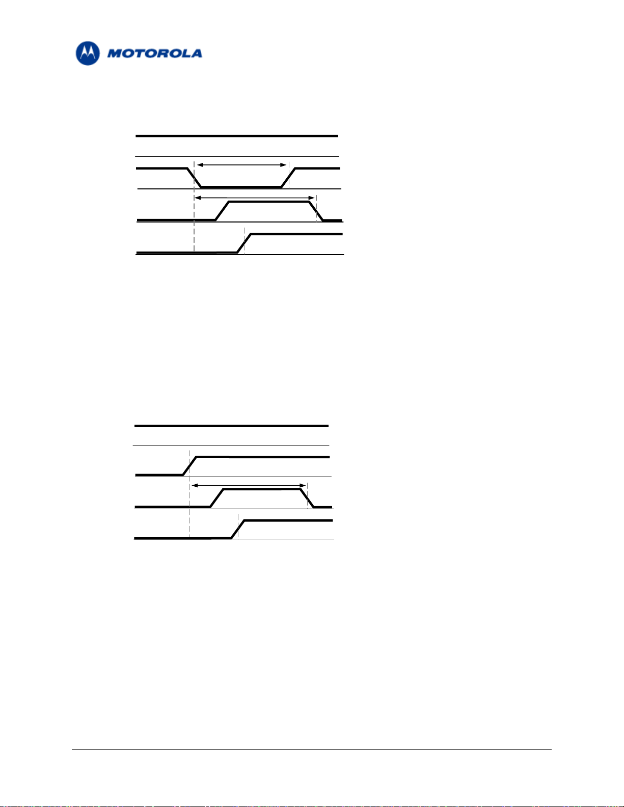
2.10.3 Wake-Up Out
The wakeup-out (WKUPO_N) signal is an active low output, which is designed to support a low
power mode feature in the host application. This signal is used by the module to indicate that it
requires to communicate with the host application through the serial interface, due to an incoming
call or data, or an unsolicited event.
The wakeup out mechanism, using the WKUPO_N signal, is controlled by 2 AT commands:
• ATS102 - Defines the delay time in milliseconds that the module will wait, after asserting the
WKUPO_N signal low, before sending data on the serial interface. This delay is required to
allow the application enough time to reactivate from low power mode and switch to normal
Motorola General Business Use
Page 33 of 36
Page 34

C24 Hardware Interface Manual
A
A
A
Applicant: Motorola, INC
FCC ID: IHDP56JE1
mode. If ATS102=0, which is the default value, the WKUPO_N signal and mechanism is
disabled.
In case the serial interface incorporates hardware flow control signals, the data will be sent
according to their state, after the ATS102 delay time has expired.
• ATS100 - Defines the application minimal wakeup duration, in Seconds, for a single wakeup
event. This time definition is required to avoid frequent unnecessary wakeup events and
consequent ATS102 delays.
The application may return to low power mode after the serial interface has been inactive for
the duration set by ATS100. This duration is measured from the last data sent or received on
the serial interface.
The following guidelines apply to the wakeup-out mechanism:
• The module will set the WKUPO_N signal low to indicate that in has data to send through the
serial interface.
• The module will start sending the data to the application after the delay defined by ATS102.
• The WKUPO_N signal will remain low while data is being sent to the host application.
• The host application should keep its serial interface active, and not switch to low power mode,
while the WKUPO_N signal is low.
• The module will set the WKUPO_N signal high when it has completed sending the data.
• The application serial interface must stay active, and not switch to low power mode, for the
duration set by ATS100, after WKUPO_N is set high.
• The module will not set the WKUPO_N signal low if it needs to send additional data during the
ATS100 delay time.
• The application may switch to low power mode after the WKUPO_N signal is set high and the
serial interface has been inactive for the duration set by ATS100.
FIGURE 25 – WKUPO_N operation
WKUPO_N
pplication
TS102
Sleep
Idle
TS100
Version 0.3
RXD_N
2.10.4 Antenna Detection
The module incorporates an internal antenna detection circuit, which senses the physical connection and
removal of an antenna or antenna circuit on the module’s antenna connector. The antenna detection state
is reported to the application through the ANT_DET output signal, and may also be queried by the ATS97
command.
The detection circuit senses DC resistance to ground on the module’s antenna connector.
A DC resistance below 100KΩ (± 5%) is defined as a valid antenna connection, and the ANT_DET output
signal is set high.
A DC resistance above 100KΩ (± 5%) is defined as an antenna disconnection, and the ANT_DET output
is set low.
Motorola General Business Use
Page 34 of 36
Page 35

C24 Hardware Interface Manual
Applicant: Motorola, INC
FCC ID: IHDP56JE1
Version 0.3
2.10.5 CDMA NW Detection
The CDMA output signal indicates the network CDMA connection status. When module is
connected to a CDMA network, this signal is enabled. When module is not connected to the
module network this signal is disabled.
2.10.6 Transmission Indicator
The TXEN_N output signal indicates when the module is transmitting over the CDMA network. This signal
follows the module’s transmit bursts. This signal is set low during transmission, and set high when no
transmission is in progress.
2.10.7 General Purpose I/O
The module incorporates 8 general purpose IO signals for the user application. Each GPIO signal may be
configured and controlled by AT command. These signals may be used to control or set external
application circuits, or to receive indications from the external application.
Each GPIO shall have internal pull-up resistor of 6KΩ (± 5%
Motorola General Business Use
Page 35 of 36
Page 36

C24 Hardware Interface Manual
Applicant: Motorola, INC
FCC ID: IHDP56JE1
Version 0.3
2.11 Antenna Interface
The module’s antenna connector is the RF interface to the network.
The antenna interface is terminated by an MMCX connector type, which is 50Ω impedance matched at
the relevant frequencies.
The antenna or antenna application must be installed properly to achieve best performance.
TABLE 25 – Antenna Interface Specifications
Parameter Conditions Specifications
1900 MHz
Sensitivity
800 MHz
RF output
power
1900 MHz
800 MHz
Gain 0 dBi (unity) gain or greater
Impedance 50Ω
VSWR Less than 2.5:1
-106dBm
-106dBm
Max Average Power Max Peak Power
25dBm 30dBm
25dBm 30dBm
Motorola General Business Use
Page 36 of 36
 Loading...