MOTOROLA NCP566ST25T3G, NCP566 Datasheet

NCP566
1.5 A Low Dropout
Linear Regulator
The NCP566 low dropout linear regulator will provide 1.5 A at a
fixed output voltage. The fast loop response and low dropout voltage
make this regulator ideal for applications where low voltage and good
load transient response are important. Device protection includes
current limit, short circuit protection, and thermal shutdown.
Features
• Ultra Fast Transient Response (t1.0 ms)
• Low Ground Current (1.5 mA @ Iout = 1.5 A)
• Low Dropout Voltage (0.9 V @ Iout = 1.5 A)
• Low Noise (37 mVrms)
• 1.2 V, 1.8 V, 2.5 V Fixed Output Versions.
Other Fixed Voltages Available on Request
• Current Limit Protection
• Thermal Shutdown Protection
• These are Pb−Free Devices
Typical Applications
• Servers
• ASIC Power Supplies
• Post Regulation for Power Supplies
• Constant Current Source
• DTV
• LCD Monitors
• Networking Equipment
• Battery Powered Systems
• Motherboards
• Peripheral Cards
• Set Top Boxes
• Medical Equipment
• Notebook Computers
http://onsemi.com
MARKING
DIAGRAMS
SOT−223
CASE 318E
xx = Voltage Rating
12 = 1.2 V
18 = 1.8 V
25 = 2.5 V
A = Assembly Location
Y = Year
M = Date Code
G = Pb−Free Package
(Note: Microdot may be in either location)
PIN CONNECTIONS
V
1
in
2
GND
V
3
out
See detailed ordering and shipping information in the package
dimensions section on page 9 of this data sheet.
ORDERING INFORMATION
AYM
566xx G
G
1
GND
© Semiconductor Components Industries, LLC, 2007
March, 2007 − Rev. 1
1 Publication Order Number:
NCP566/D

NCP566
PIN DESCRIPTION
Pin No. Symbol Description
1
2, Tab
3
MAXIMUM RATINGS
Input Voltage (Note 1) V
Output Pin Voltage V
Thermal Characteristics (Notes 2, 3)
Thermal Resistance, Junction−to−Ambient
Thermal Resistance, Junction−to−Pin
Operating Junction Temperature Range T
Operating Ambient Temperature Range T
Storage Temperature Range T
Stresses exceeding Maximum Ratings may damage the device. Maximum Ratings are stress ratings only. Functional operation above the
Recommended Operating Conditions is not implied. Extended exposure to stresses above the Recommended Operating Conditions may affect
device reliability.
1. This device series contains ESD protection and exceeds the following tests:
Human Body Model JESD 22−A114−B
Machine Model JESD 22−A115−A
2. The maximum package power dissipation is:
3. As measured using a copper heat spreading area of 50 mm2, 1 oz copper thickness.
T
P
+
D
J(max)
R
qJA
* T
A
V
in
Ground
V
out
Positive Power Supply Input Voltage
Power Supply Ground
Regulated Output Voltage
Rating Symbol Value Unit
in
out
9.0 V
−0.3 to Vin + 0.3 V
°C/W
R
q
JA
R
q
JP
J
A
stg
107
12
−40 to 150 °C
−40 to 125 °C
−55 to 150 °C
C
in
Voltage
Reference
V
Block
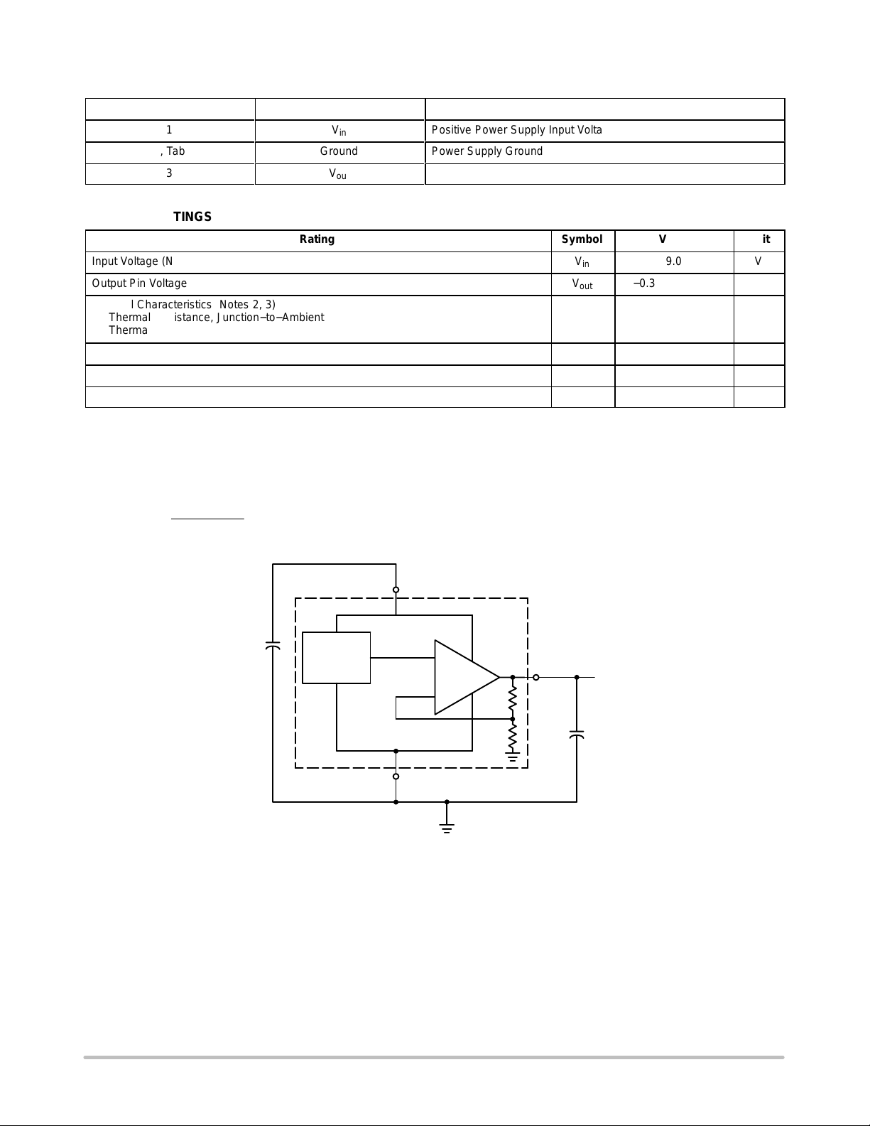
Cin − 4.7 mF to 150 mF recommended
C
− 2.2 mF to 150 mF recommended
out
See more details in Applications Information section
Figure 1. Typical Schematic
= 0.9 V
ref
V
in
GND
Output
Stage
GND
R1
R2
V
out
C
out
http://onsemi.com
2

NCP566
ELECTRICAL CHARACTERISTICS (V
+ 1.6 V, for typical values TJ = 25°C, for min/max values TJ = −40°C to +125°C,
in = Vout
(Note 4) unless otherwise noted.)
Characteristic
Output Voltage (10 mA < I
1.2 V version
Output Voltage (10 mA < I
1.2 V version
Output Voltage (10 mA < I
1.8 V version
Output Voltage (10 mA < I
1.8 V version
Output Voltage (10 mA < I
2.5 V version
Output Voltage (10 mA < I
2.5 V version
Line Regulation (I
out
Load Regulation (10 mA < I
Dropout Voltage (I
out
< 1.5 A; 2.8 V < Vin < 9.0 V; TJ = −10 to 105°C)
out
< 1.5 A; 2.8 V < Vin < 9.0 V; TJ = −40 to 125°C)
out
< 1.5 A; 3.4 V < Vin < 9.0 V; TJ = −10 to 105°C)
out
< 1.5 A; 3.4 V < Vin < 9.0 V; TJ = −40 to 125°C)
out
< 1.5 A; 4.1 V < Vin < 9.0 V; TJ = −10 to 105°C)
out
< 1.5 A; 4.1 V < Vin < 9.0 V; TJ = −40 to 125°C)
out
= 10 mA) Reg
< 1.5 A) Reg
out
= 1.5 A) (Note 5) Vdo − 0.9 1.3 V
Current Limit I
Ripple Rejection (120 Hz; I
Ripple Rejection (1 kHz; I
= 1.5 A) RR − 85 − dB
out
= 1.5 A) RR − 75 − dB
out
Symbol Min Typ Max Unit
V
out
V
out
V
out
V
out
V
out
V
out
load
lim
line
1.176
(−2%)
1.164
(−3%)
1.764
(−2%)
1.746
(−3%)
2.450
(−2%)
2.425
(−3%)
1.2 1.224
(+2%)
1.2 1.236
(+3%)
1.8 1.836
(+2%)
1.8 1.854
(+3%)
2.5 2.550
(+2%)
2.5 2.575
(+3%)
− 0.02 − %
− 0.04 − %
1.6 3.5 − A
Thermal Shutdown − 160 − °C
Ground Current (I
Output Noise Voltage (f = 100 Hz to 100 kHz, I
= 1.5 A) Iq − 1.5 3.0 mA
out
= 1.5 A) V
out
n
− 37 −
4. Refer to Application Information section for capacitor details.
5. Dropout voltage is a measurement of the minimum input/output differential at full load.
V
V
V
V
V
V
mVrms
http://onsemi.com
3
 Loading...