

MOTOROLA NCP1560HDR2 Datasheet
NCP1560
Full Featured Voltage Mode
PWM Controller
The NCP1560 PWM controller contains all the features and
flexibility needed to implement voltage-mode control in high
performance single ended DC/DC converters. This device cost
effectively reduces system part count with the inclusion of a high
voltage start-up regulator that operates over a wide input range of
21.5 V to 150 V. The NCP1560 provides two control outputs, OUT1
which controls the main PWM switch and OUT2 with adjustable
over-lap delay, which can control a synchronous rectifier switch or an
active clamp/reset switch. Other distinctive features include: two
mode over current protection, line under/over voltage lockout, fast
line feedforward, soft start and a maximum duty cycle limit.
Features
• Minimum Operating Voltage of 21.5 V
• Internal High Voltage Start-up Regulator
• Dual Control Outputs with Adjustable Overlap Delay
• Single Resistor Oscillator Frequency Setting
• Fast Line Feedforward
• Line Under/Over Voltage Lockout
• Dual Mode Over Current Protection
• Programmable Maximum Duty Cycle Control
• Maximum Duty Cycle Proportional to Line Voltage
• Programmable Soft Start
• Precision 5.0 V Reference
http://onsemi.com
MARKING
DIAGRAM
16
SO-16
16
1
ORDERING INFORMATION
Device Package Shipping
NCP1560HDR2 SO-16 2500/Tape & Reel
D SUFFIX
CASE 751B
NCP1560 = Device Code
A = Assembly Location
WL = Wafer Lot
Y = Year
WW = Work Week
NCP1560
AWLYWW
1
T ypical Applications
• Telecommunication Power Converters
• Industrial Power Converters
• High Voltage Power Modules
• +42 V Automotive Systems
• Control Driven Synchronous Rectifier Power Converters
Semiconductor Components Industries, LLC, 2003
January, 2003 - Rev. 5
1 Publication Order Number
NCP1560/D

NCP1560
UV/OV
CSKIP
DC
MAX
V
CS
R
FF
High Voltage
in
Start-up
Regulator
5.0 V
Reference
UV
Fault
Detection
T
Modulator
Delay
Logic
Output
Drivers
Oscillator
V
AUX
V
REF
OUT1
OUT2
t
D
V
EA
SS
GND
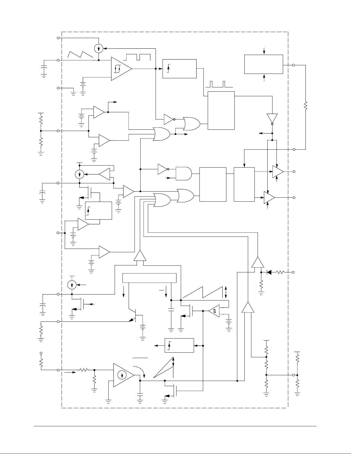
Figure 1. Simplified Block Diagram
http://onsemi.com
2
V
in
V
in
V
AUX
C
AUX
GND
UV/OV
CSKIP
C
CSKIP
CS
C
SS
R
T
R
FF
V
16
14
2
5
SS
R
FF
1
6
9
4
in
7
T
1.49 V
11 A
V
+
1.3 V*
-
I
FF
13.8 mA
+
11 V/7 V
-
+
+
-
-
+
3.6 V
-
V
REF
Disable
One Shot
Pulse
(600 ns)
+
-
+
0.6 V
-
+
0.5 V
-
REF
Disable_ss
STOP
* Trimmed during
manufacturing to obtain
1.3 V with RT = 101 k
5.3 k
6.7 k
NCP1560
Disable
One Shot
Pulse
(250 ns)
Disable_V
REF
S
Monotonic
Dominant)
Start
Latch
(Reset
Q
R
+
STOP
Disable_ss
-
+
Clock
-
+
+
2 V
-
+
+
-
Soft Start
Comparator
S
Output
Latch
(Reset
Dominant)
R
Q
Delay
Logic
CURRENT MIRROR
Oscillator Ramp
I
2 V
1
2
10 pF
One Shot
Pulse
FF Ramp
(Adjustable)
+
2 V
2 V
+
-
I
1
+
-
Clock
V
I
125 k
+
+
V
-
-
10 pF
C
FF
V
AUX
5.0 V Reference
DIS
Disable_V
V
AUX
Comparator
+
-
20 k
Max DC
+
Comparator
-
2 V
+
V
DC(inv)
-
REF
V
AUX
DIS
PWM
40 k
32 k
27 k
DIS
2 k
10
V
12
t
15
13
11
D
V
REF
R
OUT2
V
REF
8
D
OUT1
EA
R
MDP
DC
MAX
R
P
Figure 2. NCP1560 Functional Block Diagram
http://onsemi.com
3

NCP1560
PIN DESCRIPTION
Pin Name Application Information
1 V
in
2 UV/OV Input supply voltage is scaled down and sampled by means of a resistor divider. The supply voltage must
3 NC Not Connected.
4 FF An external resistor between Vin and this pin adjusts the amplitude of the FF Ramp in proportion to Vin. By
5 CS Over current sense input. If the CS voltage exceeds 0.48 V or 0.57 V, the converter enters the Cycle by
This pin is connected to the bulk DC input voltage supply. A constant current source supplies current from
this pin to the capacitor connected on the V
range is 21.5 V to 150 V.
pin. The charge current is typically 13.8 mA. Input voltage
AUX
be scaled down between 1.52 V and 3.61 V within the specified input voltage range.
varying the feedforward ramp amplitude in proportion to the input voltage, changes in loop bandwidth are
eliminated.
Cycle or Cycle Skip current limit mode, respectively.
6 CSKIP The capacitor connected between this pin and ground sets the Cycle Skip period. A soft start sequence
follows at the conclusion of the fault period.
7 R
8 DC
T
MAX
A single external resistor between this pin and GND sets the oscillator fixed frequency.
An external resistor between this pin and GND sets the voltage on the Max DC Comparator inverting in-
put. The duty cycle is limited by comparing the voltage on the Max DC Comparator inverting input to the
Feedforward Ramp.
9 SS An internal 6.2 A current source charges the external capacitor connected to this pin. The duty cycle is
limited during start-up by comparing the voltage on this pin to the Oscillator Ramp.
10 V
EA
The error signal from an external error amplifier is fed into this input and compared to the Feedforward
Ramp. A series diode and resistor offset the voltage on this pin before it is applied to the PWM Compara-
tor inverting input.
11 V
12 t
REF
D
Precision 5.0 V reference output. Maximum output current is 6 mA.
An external resistor between V
tions.
and this pin sets the overlap delay between OUT1 and OUT2 transi-
REF
13 OUT2 Output of the PWM controller with leading and trailing edge overlap delay. OUT2 can be used to drive a
synchronous rectifier topology, an active clamp/reset switch, or both.
14 GND Control circuit ground.
15 OUT1 Main output of the PWM controller.
16 V
AUX
Positive input supply voltage. This pin is connected to an external capacitor for energy storage. An inter-
nal current supplies current from Vin to this pin. Once the voltage on V
source turns OFF. It turns ON again once V
the IC via this pin, by means of an auxiliary winding.
falls to 7 V. During normal operation, power is supplied to
AUX
reaches 11 V, the current
AUX
http://onsemi.com
4

NCP1560
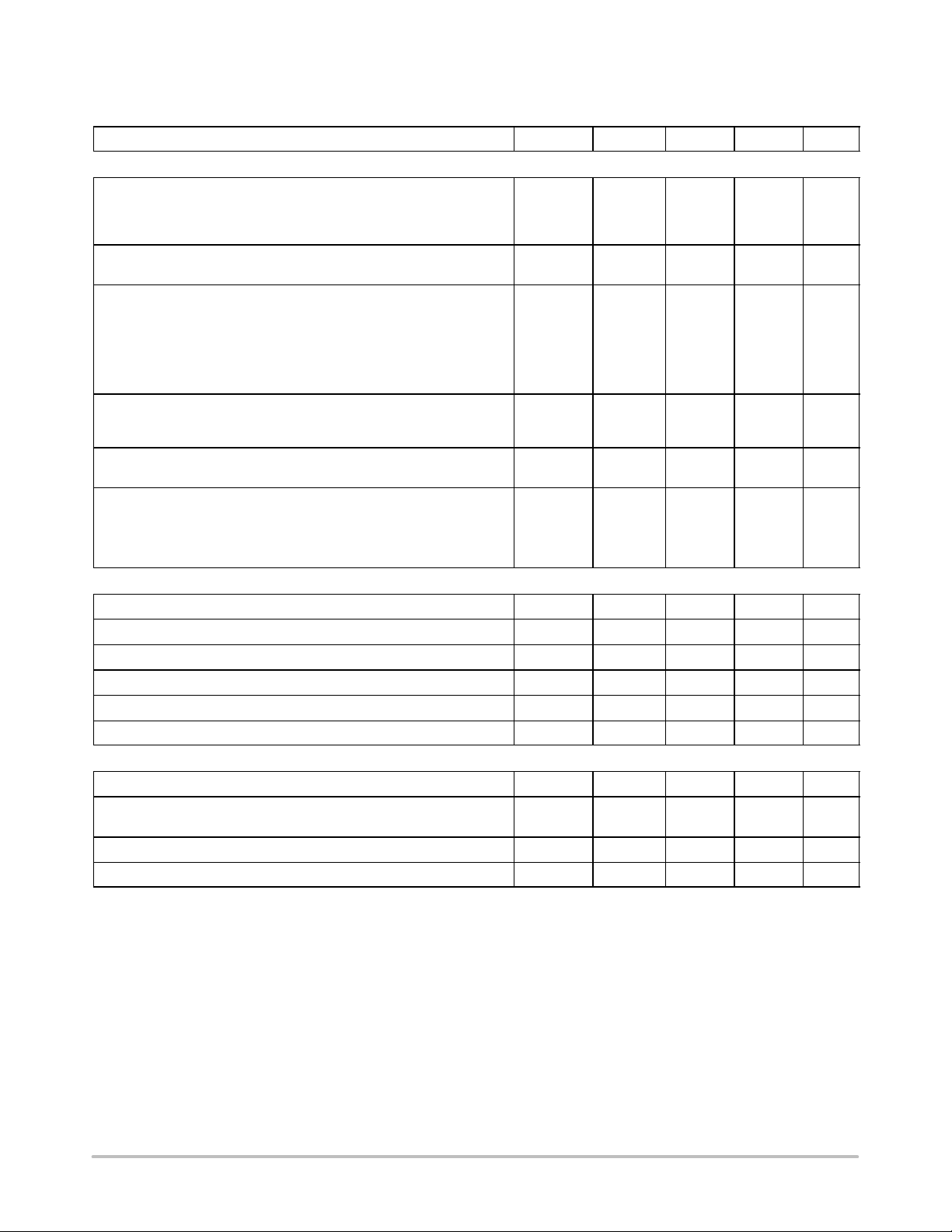
MAXIMUM RATINGS (Note 1)
Rating
Input Line Voltage V
Auxiliary Supply Voltage V
Auxiliary Supply Input Current I
OUT1 and OUT2 Voltage V
OUT1 and OUT2 Output Current I
5.0 V Reference Voltage V
5.0 V Reference Output Current I
All Other Inputs/Outputs Voltage V
All Other Inputs/Outputs Current I
Operating Junction Temperature T
Storage Temperature Range T
Power Dissipation at TA = 25°C P
Thermal Resistance, Junction to Ambient R
1. Maximum Ratings are those values beyond which damage to the device may occur. Exposure to these conditions or conditions beyond those
indicated may adversely affect device reliability. Functional operation under absolute maximum-rated conditions is not implied. Functional
operation should be restricted to the Recommended Operating Conditions.
A.This device series contains ESD protection and exceeds the following tests:
Pin 1 is the HV start-up of the device and is rated to the max rating of the part, or 150 V.
Machine Model Method 150 V.
Pins 2-16: Human Body Model 4000 V per MIL-STD-883, Method 3015.
Machine Model Method 200 V.
Symbol Value Unit
in
AUX
AUX
OUT
OUT
REF
REF
IO
IO
stg
D
J
JA
-0.3 to 150 V
-0.3 to 16 V
35 mA
-0.3 to (V
+ 0.3 V) V
AUX
10 mA
-0.3 to 6.0 V
6.0 mA
-0.3 to V
REF
10 mA
-40 to 125 °C
-55 to 150 °C
0.77 W
130 °C/W
V
http://onsemi.com
5
NCP1560
ELECTRICAL CHARACTERISTICS (V
R
= 60.4 k, RFF = 432 k, for typical values TJ = 25°C, for min/max values, TJ = -40°C to 125°C, unless otherwise noted)
D
Characteristic
START-UP CONTROL AND V
Regulation
V
AUX
Start-up Threshold/V
Minimum Operating V
Hysteresis
AUX
AUX
Minimum Start-up Voltage (Pin 1)
I
START
= 1.0 mA, V
AUX
= V
Start-up Circuit Output Current
V
= 0 V
AUX
T
= 25°C
J
T
= -40°C to 125°C
J
= V
V
AUX
TJ = 25°C
T
= -40°C to 125°C
J
AUX(on)
- 0.2 V
Start-up Circuit Off-State Leakage Current (Vin = 150 V)
TJ = 25°C
T
= -40°C to 125°C
J
Start-up Circuit Breakdown Voltage (Note 2)
I
START(off)
= 50A, TJ = 25°C
Auxiliary Supply Current After V
Outputs Disabled
V
= 0 V
EA
= 0.7 V
V
UV/OV
Outputs Enabled
REGULATOR
AUX
Regulation Peak (V
Valley Voltage After Turn-On
- 0.2 V
AUX(on)
Turn-On
AUX
= 48 V, V
in
AUX
= 12 V, VEA = 2 V, RT = 101 k, C
AUX
Symbol Min Typ Max Unit
increasing)
V
V
V
START(min)
I
START(off)
AUX(on)
AUX(off)
V
I
START
V
(BR)DS
I
AUX1
I
AUX2
I
AUX3
= 6800 pF,
CSKIP
10.5
6.6
H
-
11.0
7.0
4.0
- 19.3 21.5
13
10
10
8
-
-
17.5
-
13.8
-
23
-
150 - - V
-
-
-
2.7
1.3
4.6
LINE UNDER/OVERVOLTAGE DETECTOR
Undervoltage Threshold (V
Increasing) V
in
Undervoltage Hysteresis V
Overvoltage Threshold (Vin Increasing) V
Overvoltage Hysteresis V
Undervoltage Propagation Delay to Output t
Overvoltage Propagation Delay to Output t
UV
UV(H)
OV
OV(H)
UV
OV
1.40 1.52 1.64 V
0.080 0.098 0.120 V
3.47 3.61 3.75 V
- 0.145 - V
- 250 - ns
- 160 - ns
CURRENT LIMIT
Cycle by Cycle Threshold Voltage
Propagation Delay to Output (VEA = 2.0 V)
VCS = I
to 2.0 V, measured when V
LIM1
reaches 0.5 V
OUT
OH
Cycle Skip Threshold Voltage I
Cycle Skip Charge Current (V
= 0 V) I
CSKIP
I
LIM1
t
ILIM
LIM2
CSKIP
0.44 0.48 0.52 V
- 90 150 ns
0.54 0.57 0.62 V
8.0 12.3 15 A
2. Guaranteed by design only.
11.5
V
7.4
V
mA
21
25
17
19
A
50
100
mA
5.0
2.5
6.5
http://onsemi.com
6
 Loading...