NCP1205
Single Ended PWM
Controller Featuring QR
Operation and Soft
Frequency Foldback
The NCP1205 combines a true Current Mode Control modulator
and a demagnetization detector to ensure full Discontinuous
Conduction Mode in any load/line conditions and minimum drain
voltage switching (Quasi–Resonant operation, also called critical
conduction operation). With its inherent Variable Frequency Mode
(VFM), the controller decreases its operating frequency at constant
peak current whenever the output power demand diminishes.
Associated with automatic multiple valley switching, this unique
architecture guarantees minimum switching losses and the lowest
power drawn from the mains when operating at no–load conditions.
Thus, the NCP1205 is optimal for applications targeting the newest
International Energy Agency (IEA) recommendations for standby
power.
The internal High–Voltage current source provides a reliable
charging path for the VCC capacitor and ensures a clean and short
start–up sequence without deteriorating the efficiency once off.
The continuous feedback signal monitoring implemented with an
Over–Current fault Protection circuitry (OCP) makes the final design
rugged and reliable. An internal Over Voltage Protection (OVP) circuit
continuously monitors the VCC pin and stops the IC whenever its level
exceeds 36 V. The DIP14 offers an adjustable version of the OVP
threshold via an external resistive network.
Features
• Natural Drain Valley Switching for Lower EMI and Quasi–Resonant
Operation (QR)
• Smooth Frequency Foldback for Low Standby and Minimum Ripple
at Light–Load
• Adjustable Maximum Switching Frequency
• Internal 200 ns Leading Edge Blanking on Current Sense
• 250 mA Sink and Source Driver
• Wide Operating Voltages: 8.0 to 36 V
• Wide UVLO Levels: 7.2 to 15 V Typical
• Auto–Recovery Internal Short–Circuit Protection (OCP)
• Integrated 3.0 mA Typ. Start–Up Source
• Current Mode Control
• Adjustable Over–Voltage Level
• Available in DIP8 and DIP14 Package
http://onsemi.com
MARKING
DIAGRAMS
8
1
1
14
NCP1205P2
1
NCP1205P
YYWW
AWLYYWW
PDIP–8
8
1
14
1
ORDERING INFORMATION
Device Package Shipping
NCP1205P PDIP–8 50 Units/Rail
NCP1205P2 PDIP–14 25 Units/Rail
N SUFFIX
CASE 626
PDIP–14
P SUFFIX
CASE 646
A = Assembly Location
WL = Wafer Lot
YY = Year
WW = Work Week
AWL
Applications
• High Power AC/DC Adapters for Notebooks, etc.
• Offline Battery Chargers
• Power Supplies for DVD, CD Players, TVs, Set–Top Boxes, etc.
• Auxiliary Power Supplies (USB, Appliances, etc.)
Semiconductor Components Industries, LLC, 2002
April, 2002 – Rev. 2
1 Publication Order Number:
NCP1205/D
NCP1205
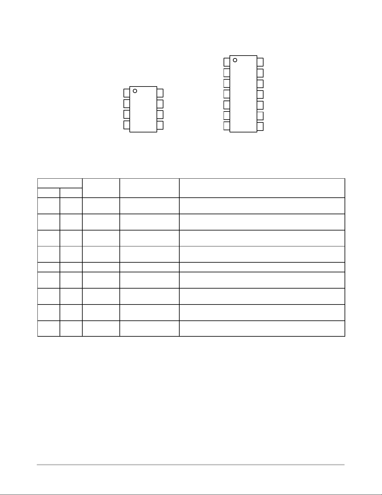
PIN CONNECTIONS
HV
Demag
FB
Ct
1
2
3
4
PDIP–8
8
7
6
5
V
CC
Drive
Isense
GND
HV
NC
Demag
FB
Ct
OVP
NC
1
2
3
4
5
6
7
PDIP–14
14
13
12
11
10
9
8
NC
V
CC
Drive
Isense
GND
NC
NC
PIN FUNCTION DESCRIPTION
Pin No.
DIP8 DIP14
1 1 HV Start–up rail Connected to the rectified HV rail, this pin provides a charging path to
2 3 Demag Zero primary–current
3 4 FB Feedback signal to
4 5 Ct Timing capacitor By adding a capacitor from Ct to the ground, the user selects the
5 10 Gnd The IC’s ground –
NA 6 OVP Overvoltage input By applying a 2.8 V typical level on this pin, the IC is permanently
6 11 Isense The primary–current
7 12 Drv This pin drives the
8 13 V
1. DIP14 has different pinouts. Please see Pin Connections.
2. Pin 2, 7, 8, 9 and 14 are nonconnected on DIP14.
Pin Name Function Description
V
bulk capacitor.
CC
This pin ensures the re–start of the main switcher when operating in
detection
free–run.
This level modulates the peak current level in free–running operation
control the PWM
and modulates the frequency in VFM operation.
minimum/maximum operating frequency.
latched–off until V
falls below UVLOL.
CC
This pin senses the primary current via an external shunt resistor.
sensing pin
The IC is able to deliver or absorb 250 mA peak currents while
CC
external switcher
Powers the IC A positive voltage up to 40 V
delivering a clamped driving signal.
typical
can be applied upon this pin
before the IC stops.
http://onsemi.com
2
4x1N4007
R5
15
Universal Input
+
C1
10 µF
R8
22 k
* R10
15 k
1
2
NCP1205P
3
4
NCP1205
R2
150
+
C14
22 µF
8
7
6
5
R4
10
D2
1N4148
M2
MTD1N60E
D6
1N5819
IC4
C10
470 µF
10 V
D7
5.1 V
L2
10 µH
++
C11
100 µF
10 V
5 V
4x1N4007
R5
15
Universal Input
C12
R6
1 nF
4.7 k
* Please refer to the application information section regarding this element.
R3
3.3
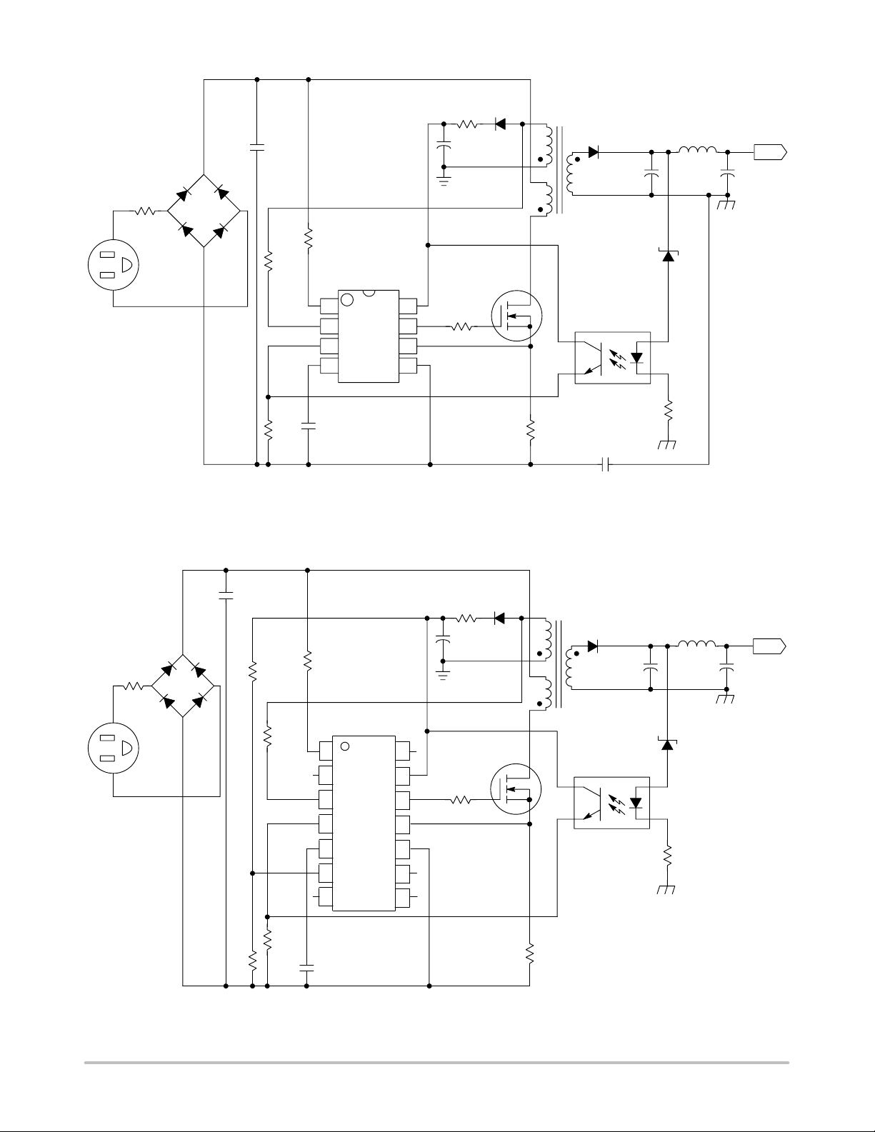
Figure 1. Typical Application Example for DIP8 Version
+
C1
10 µF
R8
22 k
* R10
15 k
NCP1205P2
1 14
2
3
4
5
6
7
13
12
11
10
9
8
D2
R2
1N4148
15
+
C14
33 µF/35 V
M2
MTD1N60E
R4
6.8
SFH6156–2
C13
1.5 nF Y1
D6
1N5819
C10
470 µF
10 V
IC4
SFH6156–2
R1
560
L2
10 µH
D7
4.3 V
R1
560
++
C11
47 µF
10 V
5 V
R6
2.7 k
C12
ROVPL ROVPU
* Please refer to the application information section regarding this element.
1 nF
Figure 2. Typical Application Example for DIP14 Version
http://onsemi.com
3
R3
3.3
NCP1205
Startup
HV
Demag
FB
Ct
1
2
Protection (V
> 40 V)
CC
Last Pulse of Demag
after 4 µs
DEMAG ?
Internal V
CC
Internal Regulator
Rf
V
Max = 3 V
err
V
Min = 10 mV
Over Voltage
Ri
3
–
+
+
2.5 V
–
4 5
err
1/3
Current Comparator
–
+
250 mV – 1 V
Max Setpoint
Clock
Flip–Flop
RQ
D
UVLO
= 15 V
H
UVLO
= 7.2 V
L
Internal Clamp
Driver
200 ns L.E.B
Over Current
Protection (OCP)
V(–) < 1.5 V
+
–
Lasts more than 128 ms?
––> Protection Circuitry
1 V
250 mV Clamp
V
Pin 8
CC
err
VCO Feedback
T
= f (V
off
err
= f (Ct)
Max T
off
)
35 V Zener
V
+
OVP
–
18 k
+
2.8 V
–
8
V
CC
7
DRV
6
I
sense
Gnd
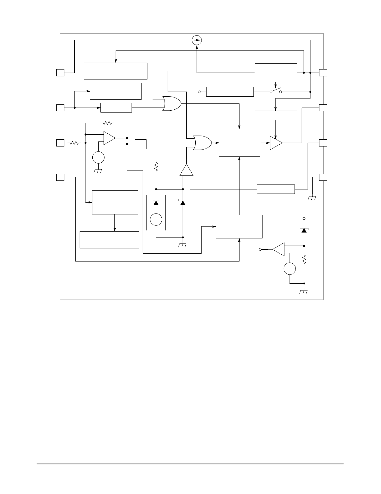
Figure 3. Internal Circuit Architecture for DIP8 Version
http://onsemi.com
4
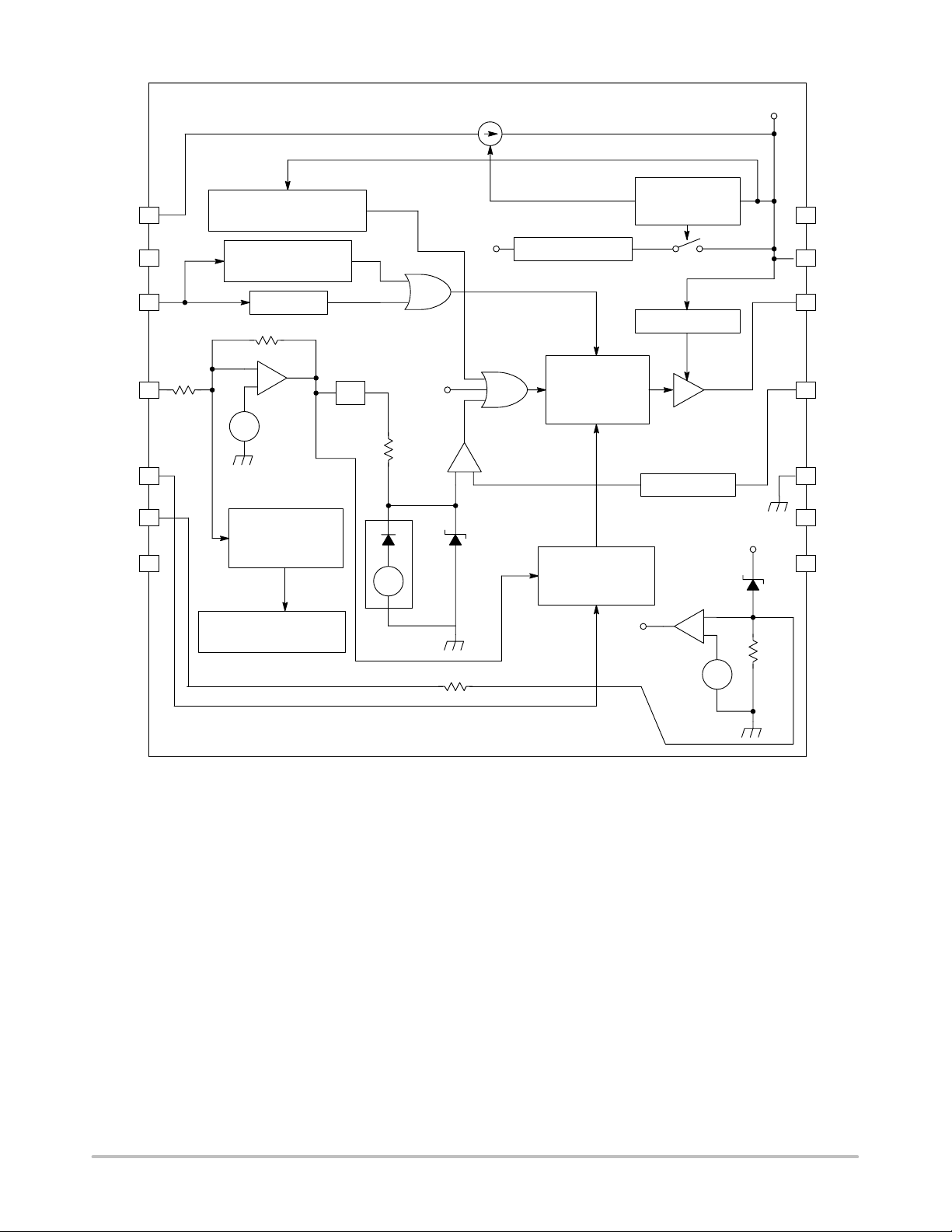
HV
NC
NCP1205
V
Pin 13
CC
Startup
UVLO
= 15 V
1
2
Protection (V
Last Pulse of Demag
after 4 µs
> 40 V)
CC
Internal V
CC
Internal Regulator
Over Voltage
UVLO
H
= 7.2 V
L
14
13
V
CC
Demag
FB
OVP
NC
Ct
3
Ri
4
5
6
7
Lasts more than 128 ms?
––> Protection Circuitry
DEMAG ?
Rf
–
+
+
2.5 V
–
Over Current
Protection (OCP)
V(–) < 1.5 V
Max = 3 V
V
err
V
Min = 10 mV
err
1/3
+
–
OVP
Current Comparator
–
+
250 mV – 1 V
Max Setpoint
1 V
250 mV Clamp
2.0 k
Internal Clamp
Clock
Flip–Flop
RQ
D
Driver
200 ns L.E.B
V
Pin 13
CC
err
VCO Feedback
T
= f (V
off
err
= f (Ct)
Max T
off
)
35 V Zener
V
+
OVP
–
18 k
+
2.8 V
–
12
11
10
DRV
I
sense
Gnd
NC
9
NC
8
Figure 4. Internal Circuit Architecture for DIP14 Version
http://onsemi.com
5
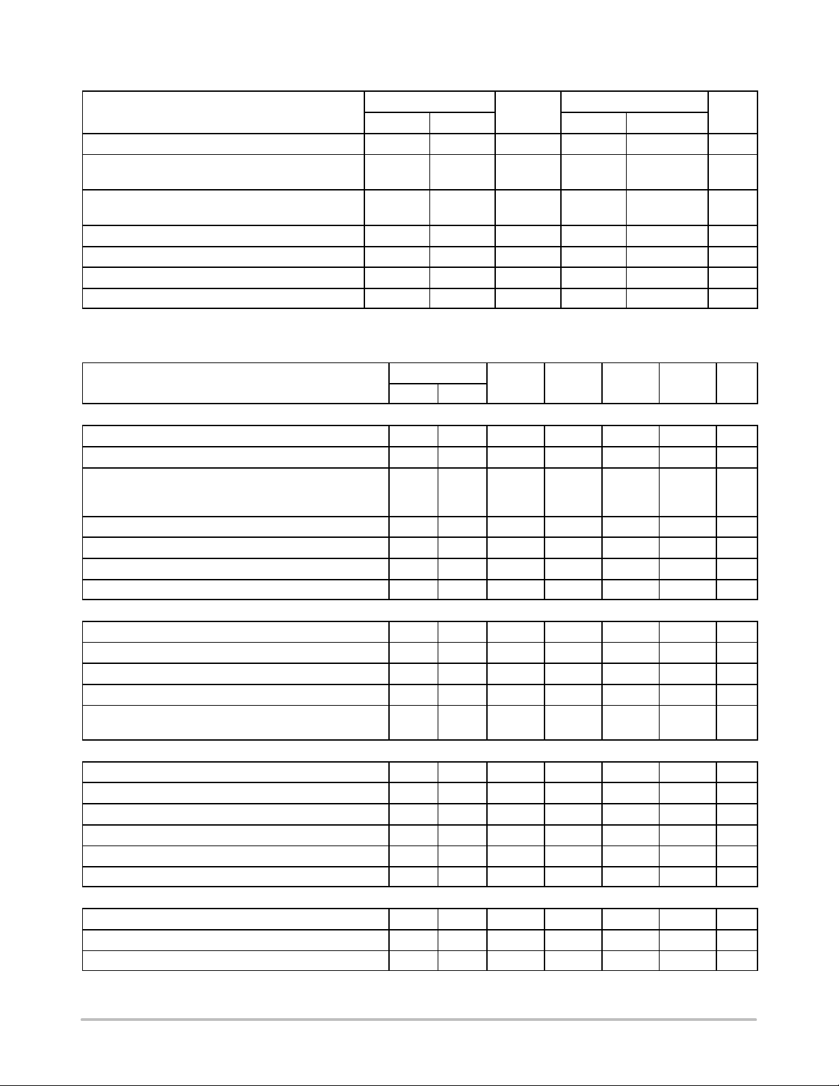
NCP1205
MAXIMUM RATINGS
Pin No.
Rating
Power Supply Voltage 8 13 V
Thermal Resistance Junction–to–Air DIP8
DIP14
Operating Junction Temperature Range
Maximum Junction Temperature
Storage Temperature Range – – T
ESD Capability, HBM Model All Pins All Pins
ESD Capability, Machine Model All Pins All Pins
DIP8 DIP14
–
–
–
–
–
–
–
–
Symbol
in
R
JA
T
J
T
Jmax
stg
–
–
Demagnetization Pin Current 3 3 – – 5.0 mA
Value
Min Max
– 45 V
–
–
–
–
100
100
–25 to +125
150
– –60 to +150 °C
– 2.0 kV
– 200 V
Unit
°C/W
°C
°C
ELECTRICAL CHARACTERISTICS (For typical values T
V
= 12 V unless otherwise noted.)
CC
= 25°C, for min/max values TJ = –25°C to +125°C, Max TJ = 150°C,
A
Pin No.
Characteristics
DIP8 DIP14
Symbol Min Typ Max Unit
Demagnetization Block
Input Threshold Voltage (V
Hysteresis (V
decreasing) 2 3 V
pin2
Input Clamp Voltage
High State (I
Low State (I
= 3.0 mA)
pin2
= –3.0 mA)
pin2
increasing) 2 3 Vth 50 65 85 mV
pin2
H
– 30 – mV
2 3
VC
VC
H
L
8.0
–0.9
10
–0.7
12
–0.5
Demag Propagation Delay – – – 100 300 350 ns
No Demag Signal Activation – – – – 4.0 8.0 µs
Internal Input Capacitance at 1.0 V 2 3 C
pin2
– 10 – pF
Demag Propagation Delay with 22 kΩ External Resistor 2 3 – 100 370 480 ns
Feedback Path
Input Impedance at V
Internal Error Amplifier Closed Loop Gain 3 4 AV
Internal Built–In Offset Voltage for Error Detection – – V
= 3.0 V 3 4 Zin – 50 – kΩ
FB
CL
ref
– –3.0 – –
2.2 2.5 2.8 V
Error Amplifier Level of VCO Take Over – – – – 1.0 – V
Internal Divider from Internal Error Amp, Pin to Current
– – – – 3.0 – –
Setpoint
V
Fault Detection Circuitry
Internal Over Current Level
– – WL
L
– 1.5 – V
Fault Time Duration to Latch Activation @ Ct = 1.0 ηF – – – – 128 – ms
Over Current Latch–Off Phase @ Ct = 1.0 ηF – – – – 1.0 – s
Hysteresis when VFB goes back into Regulation – – – – 100 – mV
VCC (Pin 8) Over Voltage Protection 8 13 OVP1 36 40 43 V
Over Voltage Protection Threshold for DIP14 Version 6 6 OVP2 2.5 2.8 3.1 V
Current Sense Comparator
Input Bias Current @ 1.0 V
Maximum Current Setpoint 6 11 V
Minimum Current Setpoint 6 11 V
6 11 I
IB
min
– 0.02 – µA
cl
0.9 1.0 1.1 V
225 250 285 mV
http://onsemi.com
6
 Loading...