

Page 1

MVME2600 Series
Single Boar d Computer
Installation and Use
V2600A/IH3
July 2001 Edition
Page 2

© Copyright 1998, 2001 Motorola, Inc.
All rights reserved.
Printed in the United States of America.
®
Motorola
AIX
PowerPC
SNAPHAT
and the Motorola symbol are registered trademarks of Motorola, Inc.
®
is a registered trademark of International Business Machines Corporation.
®
is a registered trademark of International Business Machines.
®
, TIMEKEEPER®, and ZEROPOWER® are registered trademar ks of
STMicroelectronics.
All other products ment io ned i n this document are trademarks or registered trade ma rk s of
their respective holders.
Page 3

Safety Summary
The following general safety precautions must be observed during all phases of operation, service, and repair of this
equipment. Failure to comply with these precautions or with specific warnings elsewhere in this manual could result
in personal injury or damage to the equipment.
The safety precautions listed below represent warnings of certain dangers of which Motorola is aware. You, as the user
of the product, shoul d foll ow these warni ngs and al l other sa fety pr ecauti ons nece ssary fo r the safe ope ration of the
equipment in your operating environment.
Ground the Instrument.
To minimize shock hazard, the equipment chassis and enclosure must be connected to an electrical ground. If the
equipment is su pplied wi th a three-c onductor A C power ca ble, the po wer cable m ust be plug ged into an a pproved
three-contact electrical outlet, with the grounding wire (green/yellow) reliably connected to an electrical ground
(safety ground) at the power outlet. The power jack and mating plug of the power cable meet International
Electrotechnical Commission (IEC) safety standards and local electrical regulatory codes.
Do Not Operate in an Explosive Atmosphere.
Do not operate the equipment in any explosive atmosphere such as in the presence of flammable gases or fumes.
Operation of any electrical equipment in such an environment could result in an explosion and cause injury or damage.
Keep Away From Live Circuits Inside the Equipment.
Operating personnel must not remove equipment covers. Only Factory Authorized Service Personnel or other
qualified service personnel may remove equipment covers for internal subassembly or component replacement or any
internal adjust ment. Service pe rsonnel should n ot replace compon ents with power c able connected. Under certain
conditions, dangero us voltages may exist even with the power cable remo ved. T o avoid inju ries, such pers onnel should
always disconnect power and discharge circuits before touching components.
Use Caution When Exposing or Handling a CRT.
Breakage of a Cathode-Ray Tube (CRT) causes a high-velocity scattering of glass fragments (implosion). To prevent
CRT implosion, do not handl e the CRT and avoid rough handling o r jarring of t he equipment . Handling o f a CRT
should be done only by qualified service personnel using approved safety mask and gloves.
Do Not Substitute Parts or Modify Equipment.
Do not install substitute parts or perform any unauthorized modification of the equipment. Contact your local
Motorola representative for service and repair to ensure that all safety features are maintained.
Observe Warnings in Manual.
W arn ings , such as th e exa mple be low, preced e pote ntia lly da nger ous pro cedure s thro ugh out th is manual . In struc tion s
contained in the warnings m ust be follow ed. You should also employ all ot her safety precautions w hich you dee m
necessary for the operation of the equ i pm ent in your operating environment.
To prevent serious injury or death from dangerous voltages, use extreme
caution when handling, testing, and adjusting this equipment and its
Warning
components.
Page 4

Flammability
All Motorola PWBs (printed wiring boards ) are manufactured with a flammability rating
of 94V-0 by UL-recognized manufacturers.
EMI Caution
This equipment ge ner ates, uses a nd can radi ate el ectro magne tic energy . It
!
Caution
This product contains a lithium battery to power the clock and calendar circuitry.
!
Caution
may cause or be susceptible to electromagnetic interference (EMI) if not
installed and used with adequate EMI protection.
Lithium Battery Caution
Danger of explosion if battery is re placed incorrect ly. Replace battery only
with the same or equivalent type recommended by the equipment
manufacturer. Dispose of used batteries according to the manufacturer’s
instructions.
!
Attention
!
Vorsicht
Il y a danger d’explosion s’il y a remplacement incorrect de la batterie.
Remplacer uniquement avec une batterie du même type ou d’un type
équivalent recommandé par le constructeur. Mettre au rebut les batteries
usagées conformément aux instructions du fabricant.
Explosionsgefahr bei unsachgemäßem Austausch der Ba tterie. Ersatz nur
durch denselben ode r einen vom Herstel ler empfohle nen Typ. Entsorgu ng
gebrauchter Batterien nach Angaben des Herstellers.
Page 5

CE Notice (European Community)
Motorola Compute r Group pro ducts wi th the CE mar king co mply with the EMC Dir ective
(89/336/EEC). Compliance with this directive implies conformity to the following
European Norms:
EN55022 “Limits and Methods of Meas urement of Radio Int erferen ce Chara cteri stic s
of Information Technology Equipment”; this product tested to Equipment Class B
EN50082-1:1997 “Electromag netic Compatibi lit y—Gener ic Im munity St andard , Part
1. Residential, Commercial and Light Industry”
System products al so fulf ill EN60950 ( product saf ety) which i s essenti ally the r equirement
for the Low Voltage Directive (73/23/EEC).
Board products are tested in a representative system to show compliance with the above
mentioned requirements. A proper installation in a CE-marked system will maintain the
required EMC /safety performance.
In accordance with European Community directives, a “Declaration of Conformity” has
been made and is on file within the European Union. The “Declaration of Conformity” is
available on request. Please contact your sales representative.
Notice
While reasonable efforts have been made to assure the accuracy of this document,
Motorola, Inc. a ssumes n o lia bility r esulti ng from any omissio ns in this docu ment, or from
the use of the information obtained therein. Motorola reserves the right to revise th is
document and to ma ke c hanges from time to ti me in the content hereof wi thout obligation
of Motorola to notify any person of such revision or changes.
Electronic versions of this material may be read online, downloaded for personal use, or
referenced in another document as a URL to the Motorola Computer Group website. The
text itself may not b e published commerci ally in print o r electronic for m, edited, transla ted,
or otherwise altered without the permission of Motorola, Inc.
It is possible th at t hi s publication may contain r eference to or information about Motorola
products (machines and pr ograms), progra mming, or services that are not av ailable in your
country. Such references or information must not be construed to mean that Motorola
intends to announce such Motorola products, programming, or services in your country.
Page 6

Limited and Restricted Rights Legend
If the documentation contained herein is supplied, directly or indirectly, to the U.S.
Government, the following notice shall apply unless otherwise agreed to in writing by
Motorola, Inc.
Use, duplication, or disclosure by the Government is subject to restrictions as set forth in
subparagraph (b)(3) of t he Rig hts i n Technical Data clause at DFARS 252.227-7013 (Nov .
1995) and of the Rights in Noncommerc ial Computer Software and Docume ntation c lause
at DFARS 252.227-7014 (Jun. 1995).
Motorola, Inc.
Computer Group
2900 South Diablo Way
Tempe, Arizona 85282
Page 7

Contents
About This Manual
Summary of Changes...............................................................................................xviii
Overview of Contents..............................................................................................xviii
Comments and Suggestions.......................................................................................xix
Conventions Used in This Manual..............................................................................xx
CHAPTER 1 Hardware Preparation and Installation
Introduction ................................................................................................................1-1
Equipment Required ..................................................................................................1-3
Overview of Startup Procedure..................................................................................1-3
Unpacking Instructions..............................................................................................1-5
Hardware Configuration ............................................................................................1-5
MVME2603/2604 Base Board Preparation...............................................................1-6
Cache Mode Control (J3)....................................................................................1-7
Flash Bank Selection (J10).................................................................................1-7
Serial Port 4 Receive Clock Configuration (J16)...............................................1-8
Serial Port 4 Transmit Clock Configuration (J17)............................................1-10
Serial Port 4 Transmit Clock Receiver Buffer Control (J20)............................1-11
Serial Port 3 Transmit Clock Configuration (J18)............................................1-12
System Controller Selection (J22)....................................................................1-13
Remote Status and Control...............................................................................1-14
MVME712M Transition Module Preparation .........................................................1-14
Serial Ports 1-4 DCE/DTE Configuration........................................................1-17
Serial Port 4 Clock Configuration ....................................................................1-17
P2 Adapter Preparation.....................................................................................1-24
MVME761 Transition Module Preparation.............................................................1-25
Serial Ports 1 and 2...........................................................................................1-27
Configuration of Serial Ports 3 and 4...............................................................1-27
P2 Adapter Preparation (Three-Row)...............................................................1-32
P2 Adapter Preparation (Five-Row).................................................................1-33
Hardware Installation...............................................................................................1-35
RAM200 Memory Mezzanine Installation.......................................................1-35
PMC Module Installation..................................................................................1-37
PMC Carrier Board Installation........................................................................1-40
MVME2603/2604 VME Module Installation...................................................1-42
vii
Page 8

MVME712M Transition Module Installation .................................................. 1-44
MVME761 Transition Module Installation......................................................1-48
System Considerations ............................................................................................1-50
MVME2603/2604 VME Module.....................................................................1-51
CHAPTER 2 Operating Instructions
Introduction ...............................................................................................................2-1
Applying Power.........................................................................................................2-1
ABORT Switch (S1)...........................................................................................2-3
RESET Switch (S2)............................................................................................2-3
Front Panel Indicators (DS1 – DS6)...................................................................2-4
Memory Maps......................................................................... ...................................2-5
Processor Memory Map ....................................................... ...... ........................2-5
Default Processor Memory Map.................................................................2-6
PCI Local Bus Memory Map.............................................................................2-7
VMEbus Memory Map .................................. ..... ...... ........................................ .2-7
Programming Considerations....................................................................................2-8
PCI Arbitration.................................................................................................2-10
Interrupt Handling............................................................................................2-11
DMA Channels.................................................................................................2-13
Sources of Reset...............................................................................................2-13
Endian Issues....................................................................................................2-15
Processor/Memory Domain ............................... ...... .................................2-15
PCI Domain...............................................................................................2-15
VMEbus Domain .............................. ...... ....................................... ...........2-16
CHAPTER 3 Functional Description
Introduction ...............................................................................................................3-1
Features......................................................................................................................3-1
General Description...................................................................................................3-3
Block Diagram...........................................................................................................3-4
SCSI Interface ....................................................................................................3-5
SCSI Termination........................................................................................3-5
Ethernet Interface...............................................................................................3-6
PCI Mezzanine Interface....................................................................................3-7
VMEbus Interface ............................................... ........................................ .......3-8
ISA Super I/O Device (ISASIO)........................................................................3-8
Asynchronous Serial Ports..........................................................................3-9
Parallel Port.................................................................................................3-9
viii
Page 9

Disk Drive Controller................................................................................3-10
Keyboard and Mouse Interface..................................................................3-10
PCI-ISA Bridge (PIB) Controller.....................................................................3-10
Real-Time Clock/NVRAM/Timer Function.....................................................3-11
Programmable Timers.......................................................................................3-12
Interval Timers ..........................................................................................3-12
16-Bit Timers.............................................................................................3-13
Serial Communications Interface......................................................................3-13
Z8536 CIO Device.....................................................................................3-14
Base Module Feature Register..........................................................................3-14
P2 Signal Multiplexing.....................................................................................3-15
ABORT Switch (S1).........................................................................................3-16
RESET Switch (S2)..........................................................................................3-16
Front Panel Indicators (DS1 – DS6).................................................................3-17
Polyswitches (Resettable Fuses).......................................................................3-18
I/O Power...................................................................................................3-18
Speaker Control................................................................................................3-19
PM603/604 Processor.......................................................................................3-19
Flash Memory............................................................................................3-20
RAM200 Memory Module...............................................................................3-20
MVME712M Transition Module......................................................................3-21
MVME761 Transition Module .........................................................................3-22
Serial Interface Modules............................................................................3-22
CHAPTER 4 Connector Pin Assignments
MVME2603/2604 Connectors...................................................................................4-1
Common Connectors .................................................................................................4-3
LED Mezzanine Connector J1............................................................................4-3
Debug Connector J2............................................................................................4-4
Floppy/LED Connector J4..................................................................................4-7
PCI Expansion Connector J5..............................................................................4-8
Keyboard and Mouse Connectors J6, J8...........................................................4-11
DRAM Mezzanine Connector J7......................................................................4-12
PCI Mezzanine Card Connectors......................................................................4-15
VMEbus Connector P1......................... ........................................ ....................4-18
MVME712M-Compatible Versions.........................................................................4-19
VMEbus Connector P2......................... ........................................ ....................4-19
SCSI Connector ................................................................................................4-21
Serial Ports 1-4..................................................................................................4-22
Parallel Connector.............................................................................................4-23
ix
Page 10

Ethernet AUI Connector................................................................................... 4-24
MVME761-Compatible Versions............................................................................4-25
VMEbus Connector P2.....................................................................................4-25
Serial Ports 1 and 2...........................................................................................4-26
Serial Ports 3 and 4...........................................................................................4-27
Parallel Connector............................................................................................4-28
Ethernet 10BaseT/100BaseTX Connector.......................................................4-29
CHAPTER 5 PPCBug
Overview ...................................................................................................................5-1
Memory Requirements................................................................................ .......5-2
PPCBug Implementation....................................................................................5-2
Using the Debugger...................................................................................................5-3
Debugger Commands.........................................................................................5-4
Diagnostic Tests..................................................................................................5-8
CHAPTER 6 CNFG and ENV Commands
Overview ...................................................................................................................6-1
CNFG – Configure Board Information Block...........................................................6-2
ENV – Set Environment............................................................................................6-3
Configuring the PPCBug Parameters.................................................................6-3
Configuring the VMEbus Interface..................................................................6-12
APPENDIX A Specifications
Specifications............................................................................................................A-1
Cooling Requirements..............................................................................................A-2
FCC Compliance ......................................................................................................A-3
APPENDIX B Serial Interconnections
Introduction .............................................................................................................. B-1
Asynchronous Serial Ports................................................................................ B-1
Synchronous Serial Ports................................................................................... B-1
EIA-232-D Connections........................................................................................... B-2
Interface Characteristics....................................................................................B-5
EIA-530 Connections...............................................................................................B-6
Interface Characteristics....................................................................................B-8
Proper Grounding.....................................................................................................B-9
x
Page 11

APPENDIX C Troubleshooting CPU Boards: Solving Startup Problems
Introduction............................ ...................................................................................C-1
APPENDIX D Related Documentation
Motorola Computer Group Documents....................................................................D-1
Manufacturers’ Documents.......................................................................................D-2
Related Specifications...............................................................................................D-5
xi
Page 12

Page 13

List of Figures
Figure 1-1. MVME2603/2604 Base Board Block Diagram......................................1-2
Figure 1-2. MVME2603/2604 Switches, Headers, Connectors, Fuses, LEDs..........1-9
Figure 1-3. MVME712M Connector and Header Locations...................................1-16
Figure 1-4. J15 Clock Line Configuration...............................................................1-17
Figure 1-5. MVME712M Serial Port 1 DCE/DTE Configuration ..........................1-18
Figure 1-6. MVME712M Serial Port 2 DCE/DTE Configuration ..........................1-19
Figure 1-7. MVME712M Serial Port 3 DCE Configuration ...................................1-20
Figure 1-8. MVME712M Serial Port 3 DTE Configuration....................................1-21
Figure 1-9. MVME712M Serial Port 4 DCE Configuration ...................................1-22
Figure 1-10. MVME712M Serial Port 4 DTE Configuration..................................1-23
Figure 1-11. MVME712M P2 Adapter Component Placement...............................1-24
Figure 1-12. MVME761 Connector and Header Locations.....................................1-26
Figure 1-13. MVME761 Serial Ports 1 and 2 (DCE Only)......................................1-29
Figure 1-14. MVME761 Serial Ports 3 and 4 DCE Configuration..........................1-30
Figure 1-15. MVME761 Serial Ports 3 and 4 DTE Configuration..........................1-31
Figure 1-16. MVME761 P2 Adapter (Three-Row) Component Placement............1-33
Figure 1-17. MVME761 P2 Adapter (Five-Row) Component Placement ..............1-34
Figure 1-18. RAM200 Placement on MVME2603/2604.........................................1-37
Figure 1-19. PMC Module Placement on MVME2603/2604..................................1-39
Figure 1-20. PMC Carrier Board Placement on MVME2603/2604........................1-41
Figure 1-21. MVME712M/MVME2603/2604 Cable Connections.........................1-47
Figure 1-22. MVME761/MVME2603/2604 Cable Connections ............................1-49
Figure 2-1. PPCBug System Startup..........................................................................2-2
Figure 2-2. VMEbus Master Mapping.......................................................................2-9
Figure 2-3. MVME2603/MVME2604 Interrupt Architecture.................................2-12
Figure 3-1. MVME2603/2604 Block Diagram ..........................................................3-4
xiii
Page 14

Page 15

List of T ables
T ab le 1-1. Startup Overview................................... ...... .............................................1-3
Table 1-2. MVME712M Port/Jumper Correspondence...........................................1-17
Table 2-1. Processor Default View of the Memory Map...........................................2-6
T ab le 2-2. PCI Arbitration Assignments........................................ ...... ....................2-10
Table 2-3. IBC DMA Channel Assignments ...........................................................2-13
Table 2-4. Classes of Reset and Effectiveness.........................................................2-14
T ab le 3-1. MVME2603/2604 Features........................................................... ...........3-1
Table 3-2. P2 Multiplexing Sequence......................................................................3-15
T ab le 3-3. Fuse Assignments................................................... ...... ..........................3-18
Table 3-4. SIM Type Identification..........................................................................3-23
Table 4-1. LED Mezzanine Connector ......................................................................4-3
T ab le 4-2. Debug Connector................................... ...... ........................................ .....4-4
T ab le 4-3. Floppy/LED Connector......... ...... ...... ....................................... .................4-7
Table 4-4. PCI Expansion Connector.........................................................................4-8
T ab le 4-5. Keyboard Connector...............................................................................4-11
T ab le 4-6. Mouse Connector....................................................................................4-11
Table 4-7. DRAM Mezzanine Connector................................................................4-12
Table 4-8. PCI Mezzanine Card Connector.............................................................4-15
Table 4-8. PCI Mezzanine Card Connector (Continued).........................................4-16
Table 4-9. VMEbus Connector P1...........................................................................4-18
Table 4-10. VMEbus Connector P2 (MVME712M I/O Mode)...............................4-19
T ab le 4-11. SCSI Connector (MVME712M)...........................................................4-21
Table 4-12. Serial Connections—MVME712M Ports 1-4.......................................4-22
Table 4-13. Parallel I/O Connector (MVME712M).................................................4-23
Table 4-14. Ethernet AUI Connector (MVME712M) .............................................4-24
Table 4-15. VMEbus Connector P2 (MVME761 I/O Mode) ..................................4-25
Table 4-16. Serial Connections—Ports 1 and 2 (MVME761).................................4-26
Table 4-17. Serial Connections—Ports 3 and 4 (MVME761).................................4-27
Table 4-18. Parallel I/O Connector (MVME761)....................................................4-28
Table 4-19. Ethernet 10BaseT/100BaseTX Connector (MVME761)......................4-29
T ab le 5-1. Debugger Command s........................................ .......................................5-4
Table 5-2. Diagnostic Test Groups.............................................................................5-8
Table A-1. MVME2603/2604 Specifications ..........................................................A-1
Table B-1. EIA-232-D Interconnect Signals ............................................................B-3
xv
Page 16

Table B-2. EIA-232-D Interface Transmitter Characteristics .................................B-5
Table B-3. EIA-232-D Interface Receiver Characteristics ...................................... B-5
Table B-4. MVME761 EIA-530 Interconnect Signals ............................................B-6
Table B-5. EIA-530 Interface Transmitter Characteristics .....................................B-8
Table B-6. EIA-530 Interface Receiver Characteristics ..........................................B-9
Table C-1. Troubleshooting MVME2603/2604 Boards ..........................................C-1
xvi
Page 17

About This Manual
This manual provides general information, hardware preparation and
installation instructions, operating instructions, and a functional
description of the MVME2603/2604 family of single board computers.
As of the publication date , the information presented in t his manual applies
to the following MVME2603 and MVME2604 models:
Model Number Description
MVME2603-112 1C to
MVME2603-1161C
MVME2603-3121 to
MVME2603-3161
MVME2603-4121 to
MVME2603-4151
MVME2603-5121 to
MVME2603-5131
MVME2604-1321 to
MVME2604-1361
MVME2604-4321 to
MVME2604-4361
MVME2604-1401 to
MVME2604-1471
MVME2604-3321 to
MVME2604-3361
MVME2604-3401 to
MVME2604-3471
MVME2604-4401 to
MVME2604-4471
200 MHz MPC603, 16MB–256MB ECC DRAM,
9MB Flash
200 MHz MPC603, 16MB–256MB ECC DRAM,
9MB Flash
200 MHz MPC603, 16MB–128MB ECC DRAM,
9MB Flash
200 MHz MPC603, 16MB–32MB ECC DRAM,
9MB Flash
333 MHz MPC604, 16MB–256MB ECC DRAM,
9MB Flash
333 MHz MPC604, 16MB–256MB ECC DRAM,
9MB Flash
400 MHz MPC604, 0–512MB ECC DRAM, 9MB
Flash
400 MHz MPC604, 16MB–256MB ECC DRAM,
9MB Flash
400 MHz MPC604, 0–512MB ECC DRAM, 9MB
Flash
400 MHz MPC604, 0–512MB ECC DRAM, 9MB
Flash
xvii
Page 18
Summary of Changes
This is the third edition of the Installation and Use manual. It supersedes
the May 1998 edition and incorporates the following updates.
Date Changes Replaces
July 2001 All data referring to the VME CSR Bit Set Register
(VCSR_SET) and VME CSR Bit Clear Register
(VCSR_CLR) has been deleted. These registers of
the Universe II are unavailable for implementation
as intended by the MVME materials and the
Universe II User Manual.
Overview of Contents
Chapter 1, Hardware Preparation and Installation, provides general
information, hard wa re pr eparation and instal la tion instructions, operating
instructions, and a f unctional description of the MVME2603/2604 famil y
of single board computers.
Chapter 2, Operating Instructions, supplies information for use of the
MVME2603/2604 family of single board computers in a system
configuration.
V2600A/IH2
xviii
Chapter 3, Functio nal Description , describes the MVME2603/26 04 single
board computer on a block diagram level.
Chapter 4, Connector Pin Assignments, provides pin assignments for the
interconnect signals for the MVME2603/2604 family of single board
computers.
Chapter 5, PPCBug, describes the basics of PPCBug and its architecture,
describes the monitor (interactive command portion of the firmware) in
detail, and gives information on act ual ly us ing the PPCBug debugger and
the special commands.
Chapter 6, CNFG and ENV Commands, contains information about the
CNFG and ENV commands. These two commands are used to change
configuration information and command parameters interactively.
Page 19

Appendix A, Specifications, lists the general specifications for
MVME2603/2604 base boards.
Appendix B, Serial Interconnections, describes the MVME2603/2604
serial communications interfaces.
Appendix C, Troubleshooting CPU Boards: Solving Startup Problems,
supplies the user with troubleshooting tips before having to call for help.
Appendix D, Related Doc umentation, lists all docum entation related to the
MVME2603/2604 single board computer.
Comments and Suggestions
Motorola welcomes and appreciates your comments on its doc umentation.
We want to know what y ou think about our manuals and how we can make
them better. Mail comments to:
Motorola Computer Group
Reader Comments DW164
2900 S. Diablo Way
Tempe, Arizona 85282
You can also submit comments to the following e-mail address:
reader-comments@mcg.mot.com
In all your corres pondence , plea se li st your name, po siti on, and c ompan y.
Be sure to include the title and par t number of the manual and tell how you
used it. Then tell us your feelings about its strengths and weaknesses and
any recommendations for improvements.
xix
Page 20

Conventions Used in This Manual
The following typographical conventions are used in this document:
bold
is used for user inpu t that you t ype just as i t appears ; it is al so used for
commands, options and arguments to commands, and names of
programs, directories and files.
italic
is used for names of variables to which you assign values. Italic is also
used for comments in screen dis plays and examples, and to intr odu ce
new terms.
courier
is used for system output (for example, screen displays, reports),
examples, and system prompts.
<Enter>, <Return> or <CR>
<CR> represents the carriage return or Enter key.
Ctrl
xx
represents the Control key. Execute control characters by pressing the
Ctrl key and the letter simultaneously, for example, Ctrl-d.
Page 21

1Hardware Preparation and
Introduction
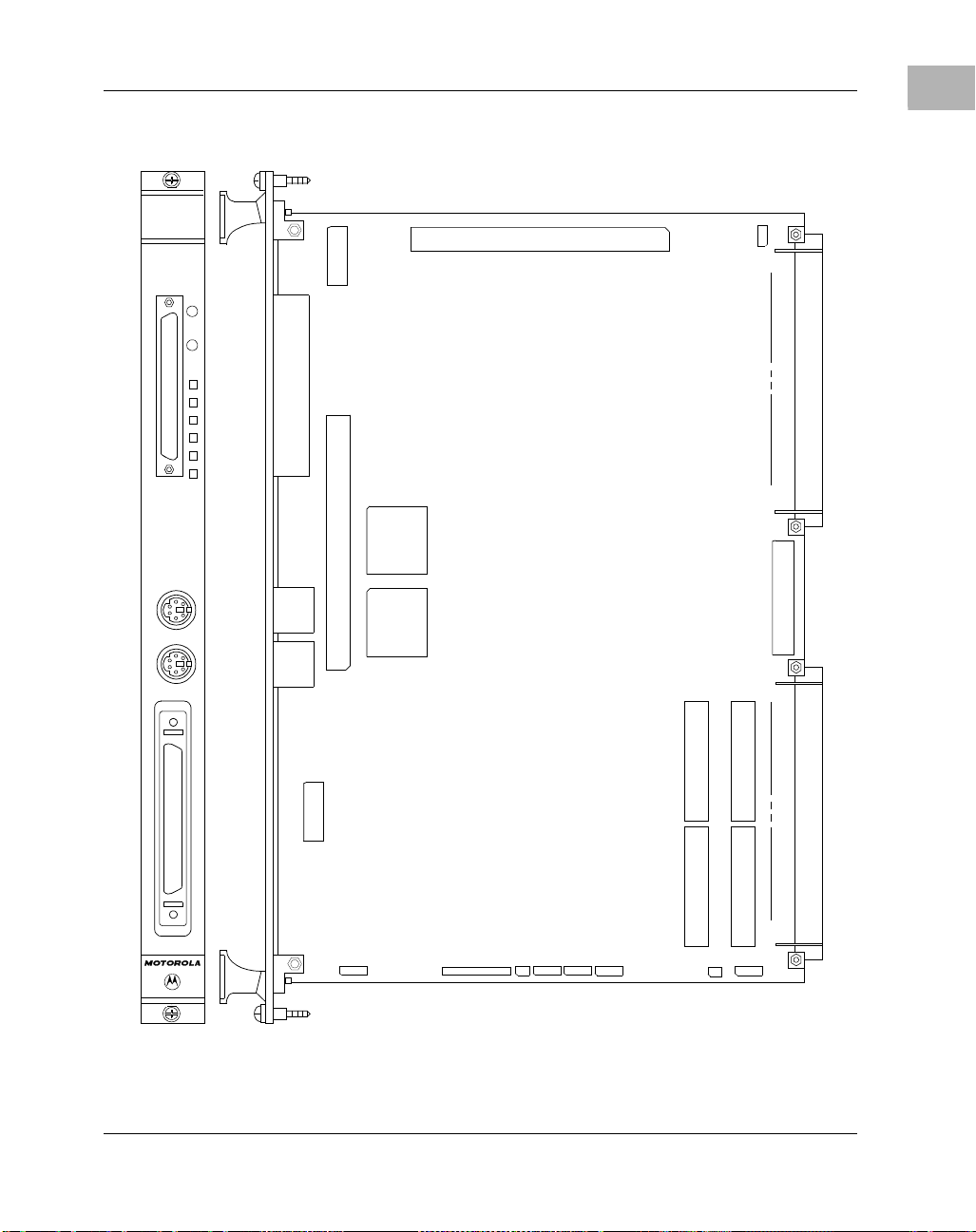
The MVME2603/2604 is a single-slot VME module equipped with a
PowerPC
PowerPC 603
microprocessor. 256KB L2 cache (level 2 secondary cache memory) is
available as an option on all versions.
The complete MVME2603/2604 consists of the base board plus:
❏ An ECC DRAM module (RAM200) for memory
❏ An optional PCI mezzanine card (PMC) for additional versatility
❏ An optional carrier board for additional PCI expansion
The block diagram in Figure 1-1 illustrates the architecture of the
MVME2603/2604 base board.
Installation
®
Series microprocessor. The MVME2603 is equipped with a
™
microprocessor; the MVME2604 has a PowerPC 604™
1
1-1
Page 22
1
Hardware Preparation and Installation
CLOCK
GENERATOR
PHB & MPIC
RAVEN ASIC
64-BIT PMC SLOT
L2 CACHE
256K
PROCESSOR
MPC603/604
REGISTERS
ISA
FLASH
1MB
MEMORY CONTROLLER
66MHz MPC604 PROCESSOR BUS
33MHz 32 /64-BIT PCI LOCAL BUS
PIB
W83C553
ISA BUS
ETHERNET
DEC21140
AUI/10BT/100BTX
RTC/NVRAM/WD
MK48T59
FALCON CHIPSET
MEMORY EXPANSION CONNECTORSDEBUG CONNECTOR
SCSI
53C825A
FLASH
4MB or 8MB
SYSTEM
REGISTERS
VME BRIDGE
UNIVERSE
BUFFERS
PCI EXPANSION
MOUSE KBD FLOPPY & LED
PMC FRONT I/O SLOT
SUPER I/O
PC87308
PARALLEL
FRONT PANEL
ESCC
85230
SERIAL
712/761 P2 I/O OPTIONS
VME P2 VME P1
CIO
Z8536
Figure 1-1. MVME2603/2604 Base Board Block Diagram
1-2 Computer Group Literature Center Web Site
Page 23
Equipment Required
The following equipment is required to complete an MVME2603/2604
system:
❏ VME system enclosure
❏ System console terminal
❏ Operating system (and/or application software)
❏ Disk drives (and/or other I/O) and controllers
❏ Transition module (MVME712M or MVME761) and connecting
cables
MVME2603/2604 VME modules are factory -configur ed for I/O handli ng
via either MVME712M or MVME761 transition modules.
Overview of Startup Procedure
Equipment Required
1
The following table li sts the th ings you will need to do bef ore you can use
this board and t ells where to find the infor mation you n eed to perform e ach
step. Be sure to rea d this entire c hapter, incl uding all Caution and Warning
notes, before you begin.
Table 1-1. Startup Overview
What you need to do... Refer to...
Unpack the hardware. Unpacking Instructions on page 1-5
Configure the hardware by setting
jumpers on the boards and transition
modules.
Ensure memory mezzanines are
properly installed on t h e bas e board.
Install the MVME2603/2604 VME
module in the chassis.
http://www.motorola.com/computer/literature 1-3
MVME2603/2604 Base Board Preparation on page 1-6
and MVME712M Transition Module Preparation on
page 1-14 or MVME761 Transition Module Preparation
on page 1-25
RAM200 Memory Mezzanine Installation on page 1-35
MVME2603/2604 VME Module Installation on page
1-42
Page 24
1
Hardware Preparation and Installation
Table 1-1. Startup Overview (Continued)
What you need to do... Refer to...
Install the transition module in the
chassis.
Connect a console terminal. System Considerations on page 1-50, MVME2603/2604
Connect any other equipment you
will be using.
Power up the system. Applying Power on page 2-1
Note that the debugger initializes
the MVME2603/ 2604.
Initialize the system clock. Using the Debugger on pag e 5-3, Debugger Commands,
Examine and/or change
environmental parameters.
Program the board as needed for
your applications.
MVME712M Transition Module Installation on page
1-44 or MVME761 Transition Module Installa tion on
page 1-48
VME module
Chapter 4, Connector Pin Assignments
For more information on optional devices and
equipment, refer to the documentation provided with the
equipment.
Appendix C, Troubleshooting CPU Boards: Solving
Startup Probl ems
Using the Debugger on pag e 5-3
You may also wish to obtain the PPCBug Firmware
Package User’s Manual, listed in Appendix D, Related
Documentation.
the SET command
Chapter 6, CNFG and ENV Commands
MVME2600 Series Single Board Computer
Programmer’s Reference Guide, listed in Appendix D,
Related Documentation.
1-4 Computer Group Literature Center Web Site
Page 25

Unpacking Instructions
Note If the shipping carton is damaged upon receipt, request that the
carrier’s agent be presen t during the unpa cking and in spection of
the equipment.
Unpack the equipment from the shipping carton. Refer to the packing list
and verify that al l items are present . Sa ve t he packing material for storing
and reshipping of equipment.
Unpacking Instructions
1
!
Caution
Avoid touching areas of integrated circuitry; static discharge can damage
circuits.
Hardware Configuration
To produce the desired configuration and ensure proper operation of the
MVME2603/2604, you may need to carry out certain hardware
modifications before installing the module.
The MVME2603/2604 provides software control over most options: by
setting bits in c ontrol re gisters after ins tallin g the modul e in a syste m, you
can modify its configurati on. (The MVME2603/2604 con trol regist ers are
described in Chapter 3, Functional Description, and/or in the MVME2600
Series Single Board Computer Programmer’s Reference Gui de, as listed in
Appendix D, Related Documentation.)
Some options, however, are not sof tware-programmabl e. Such options are
controlled through manual installation or removal of header jumpers or
interface modules on the base board or the associated transition module.
http://www.motorola.com/computer/literature 1-5
Page 26

1
Hardware Preparation and Installation
MVME2603/2604 Base Board Preparation
Figure 1-2 on page 1-9 illustrates the placement of the switches, jumper
headers, connectors, and LED indicators on the MVME2603/2604.
Manually configurable items on the base board include:
❏ Cache mode control (J3)
❏ Flash bank selection (J10)
❏ Serial Port 4 receive clock configuration (J16)
❏ Serial Port 4 transmit clock configuration (J17)
❏ Serial Port 4 transmit cl ock receiver buffer cont rol (J20)
❏ Serial Port 3 transmit clock configuration (J18)
❏ System controller selection (J22)
In conjunction with the serial port settings on the base board, serial ports
on the associated MVME712M or MVME761 transition module are also
manually configurable. For a discussion of the configurable items on the
transition module, refer to MVME712M Transition Module Preparation
on page 1-14, MVME761 Transition Mod ule Preparat ion on page 1- 25, or
to the respective user’s manuals for the transition modu les (listed in
Appendix D, Related Documentation) as necessary.
The MVME2603/2604 is factory tested and shipped with the
configurations described in the following sections. The
MVME2603/2604’s required and factory-installed debug monitor,
PPCBug, operates with those factory settings.
1-6 Computer Group Literature Center Web Site
Page 27
Cache Mode Control (J3)
256KB of L2 cache memory is available on the MVME2603/2604. L2
cache operation is transparent to users, but its write-through mode is
configurable via header J3 on older boards. On newer MVME2603/2604
boards, header J3 is not provided. With a jumper installed on J3, cache
write-through is under CPU control. With the jumper removed, cache
write-through occurs in all cases.
MVME2603/2604 Base Board Preparation
1
J3
1212
Cache Write-Through under CP U Con tro l
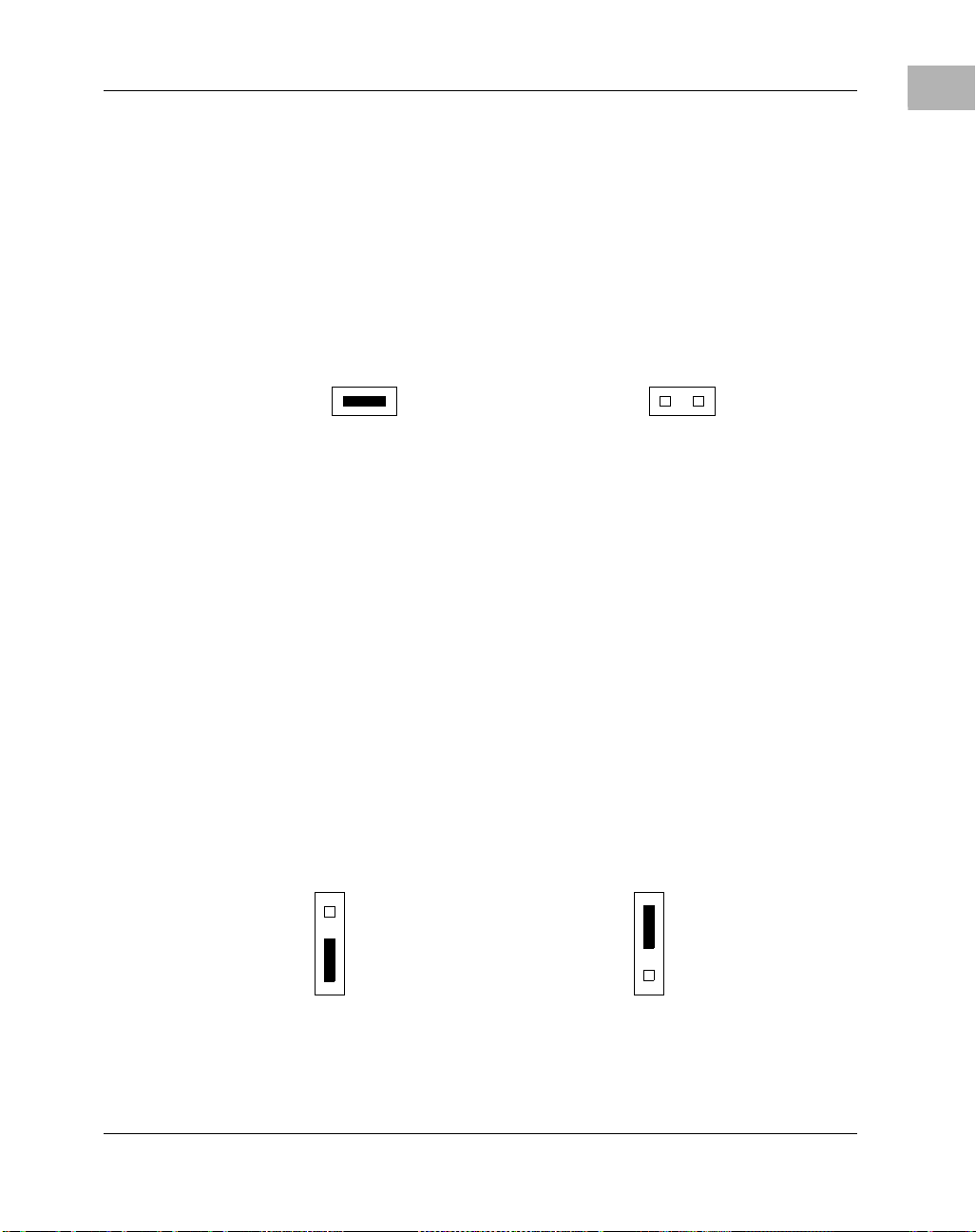
Flash Bank Selection (J10)
The MVME2603/2604 base board has provision for 1MB of 16-bit Flash
memory. The RAM200 memory mezzanine accommodat es 4MB or 8MB
of additional 64-bit Flash memory.
The Flash memory is organized in either one or two banks, each bank
either 16- or 64-bits wide. Both banks contain the onboard debugger,
PPCBug.
To enable Flash bank A (4MB or 8MB of firmware resident on solderedin devices on the RAM200 mezzani ne) , pl ace a jumper across header J10
pins 1 and 2. To enable Flas h bank B (1MB of firmware located in socket s
on the base board), place a jumper across header J10 pins 2 and 3.
J10
J3
Cache Write-Through Always
(factory configuration)
J10
3
2
1
Flash Bank A Enabled (4MB/8MB, Soldered)
(factory configuration)
Flash Bank B Enabled (1MB, Sockets)
3
2
1
http://www.motorola.com/computer/literature 1-7
Page 28
1
Hardware Preparation and Installation
Serial Port 4 Receive Clock Configuration (J16)
In synchronous seri al commun ications , you can configure Serial Port 4 on
the MVME2603/2604 to use the c lock sign als provi ded by the Rx C signal
line. On MVME712M-compatible versions of the base board, header J16
configures port 4 to either dri ve or recei ve RxC. The factory c onfiguratio n
has port 4 set t o receive RxC. J1 6 remains open o n MVME761-compatible
versions.
To complete the configura tion of Ser ial Port 4, you mus t set the f ollowing
configuration headers as well:
❏ J17 (Serial Port 4 transmit clock configuration)
❏ J20 (Serial Port 4 transmit clock receiver buffer control)
❏ J15 on the MVME712M transition modu le or J3 on the MVME761
transition module (Serial Port 4 clock configuration)
Figure 1-9 and Figure 1-10 (for the MVME712M) and Figure 1-14 and
Figure 1-15 (for the MVME761) diagram the overall jumper settings
required on the MVME2603/2604 and tran si ti on module for a Seri al Port
4 DCE or DTE configuration.
For additional details on the configuration of those headers, refer to
MVME712M Transition Module Preparation on page 1-14, MVME761
Transition Module Preparation on page 1-25, or to the respective user’s
manuals for the transition modules (listed in Appendix D, Related
Documentation) as necessary.
J16J16
3
2
1
Drive RxC
1-8 Computer Group Literature Center Web Site
3
2
1
Receive RxC
(factory configuration)
Page 29
MVME2603/2604 Base Board Preparation
1
2
1
J1
25
ABT
RST
FLOPPY/LED
CHS
BFL
CPU
PCI
FUS
SYS
244950
J4
27
2
26
1
J2
J3
A1B1C1
D1
P1
A32
B32
C32
D32
11517.00 9608
J7
KEYBOARD MOUSE
PCI MEZZANINE CARD
65
4213
J6
65
4213
J8
2
1
J9
16
15
XU1 XU2
J5
A1B1C1
2
1
2
1
J12
J11
P2
2
1
2
1
J14
J13
A32
B32
C32D1D32
64
64
J10
J15
J16
J23
J18
J17
J22
J20
Figure 1-2. MVME2603/2604 Switches, Headers, Connectors, Fuses, LEDs
http://www.motorola.com/computer/literature 1-9
Page 30
1
Hardware Preparation and Installation
Serial Port 4 Transmit Clock Configuration (J17)
In synchronous seri al commun ications , you can configure Serial Port 4 on
the MVME2603/2604 to use the clock si gnals provi ded by the TxC signa l
line. Header J17 configures port 4 to either drive or receive TxC. The
factory configuration has port 4 set to receive TxC.
To complete the configura tion of Ser ial Port 4, you mus t set the f ollowing
configuration headers as well:
❏ J16 (Serial Port 4 receive clock configuration)
❏ J20 (Serial Port 4 transmit clock receiver buffer control)
❏ J15 on the MVME712M transition modu le or J3 on the MVME761
transition module (Serial Port 4 clock configuration)
Figure 1-9 and Figure 1-10 (for the MVME712M) and Figure 1-14 and
Figure 1-15 (for the MVME761) diagram the overall jumper settings
required on the MVME2603/2604 and tran si ti on module for a Seri al Port
4 DCE or DTE configuration.
For additional details on the configuration of those headers, refer to
MVME712M Transition Module Preparation on page 1-14, MVME761
Transition Module Preparation on page 1-25, or to the respective user’s
manuals for the transition modules (listed in Appendix D, Related
Documentation) as necessary.
J17
3
2
1
Drive TxC
1-10 Computer Group Literature Center Web Site
J17
3
2
1
Receive TxC
(factory configuration)
Page 31

MVME2603/2604 Base Board Preparation
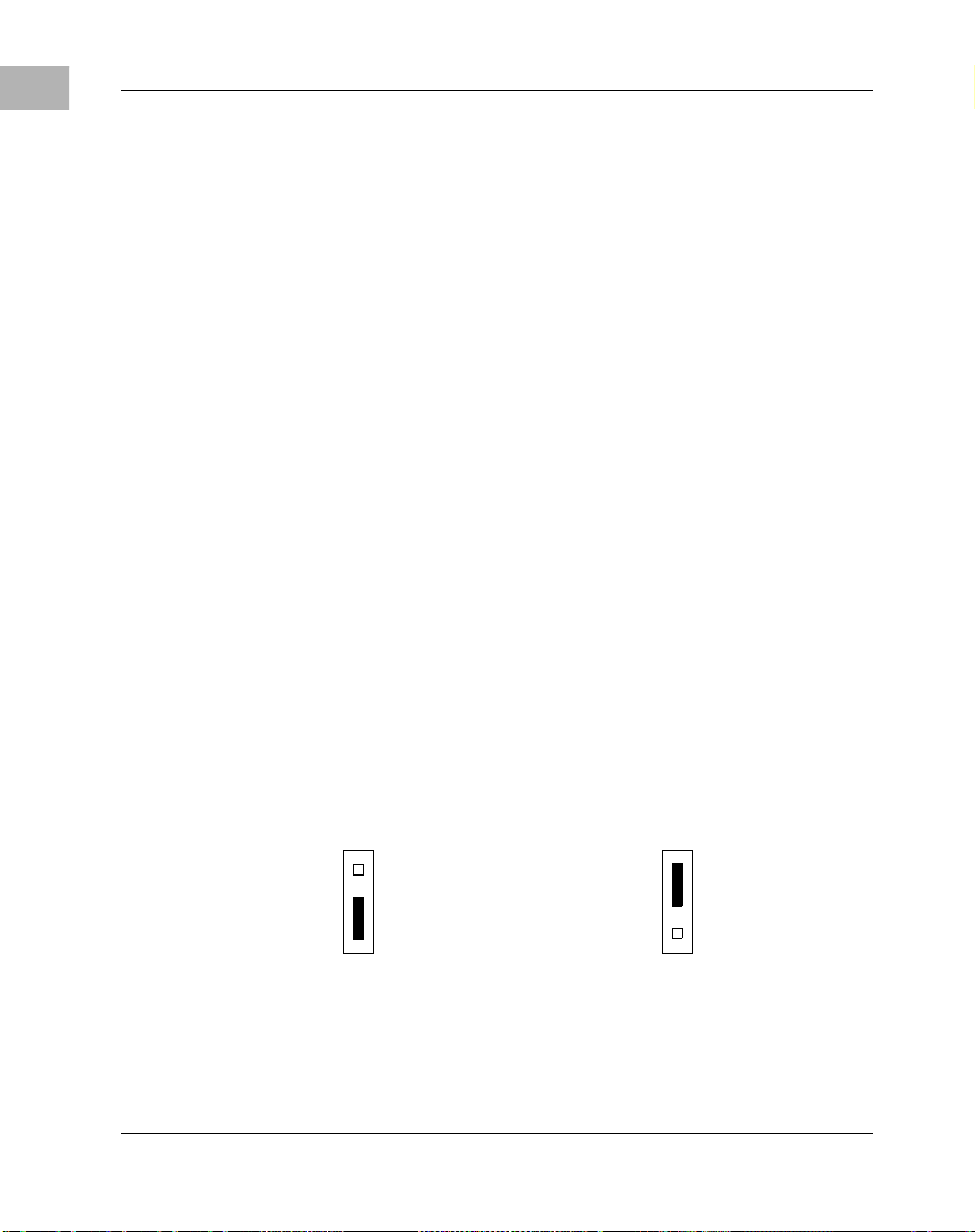
Serial Port 4 Transmit Clock Receiver Buffer Control (J20)
As described in other sections, a complete configuration of Serial Port 4
requires that you set the following jumper headers on the
MVME2603/2604 or the transition module:
❏ J16 (Serial Port 4 receive clock configuration) on MVME712M-
compatible versions of the base board
❏ J17 (Serial Port 4 transmit clock configuration)
❏ J20 (Serial Port 4 transmit clock receiver buffer control) on
MVME712M-compatible versions of the base board
❏ J15 on the MVME712M transition modu le or J3 on the MVME761
(Serial Port 4 clock configuration)
A transmit clock receiver buffer (controlled by header J20) is associated
with Serial Port 4. Inst alling a jumper on J20 enabl es the buffer. Removing
the jumper disables the buffer. The factory configuration has the Serial
Port 4 buffer enabled.
J20 remains open on MVME761-compatible versions. On MVME712Mcompatible versions, J20 is set in tandem with J17 to configure the Serial
Port 4 transmit clock. If one deviates from the factory configuration, so
must the other.
1
Figure 1-9 and Figure 1-10 (for the MVME712M) and Figure 1-14 and
Figure 1-15 (for the MVME761) diagram the overall jumper settings
required on the MVME2603/2604 and tran si ti on module for a Seri al Port
4 DCE or DTE configuration.
http://www.motorola.com/computer/literature 1-11
Page 32

1
Hardware Preparation and Installation
For additional details on the configuration of those headers, refer to
MVME712M Transition Module Preparation on page 1-14, MVME761
Transition Module Preparation on page 1-25, or to the respective user’s
manuals for the transition modules (listed in Appendix D, Related
Documentation) as necessary.
J20
2
1
Buffer Enabled
(factory configuration)
J20
2
1
Buffer Disabled
Serial Port 3 Transmit Clock Configuration (J18)
In synchronous serial communications using the MVME761 transition
module, you can configure Serial Port 3 on the MVME2603/2604 to use
the clock signals provided by the TxC signal line. On MVME761-
compatible versions of the base board, header J18 configures port 3 to
either drive or receive TxC. The factory configuration has port 3 set to
receive TxC. J18 remains open on MVME712M-compatible versions.
To complete the configuration of Serial Port 3, you must set J2 on the
MVME761 transition module (Serial Port 3 clock configuration) as well.
Figure 1-7 and Figure 1-8 (for the MVME712M) and Figure 1-14 and
Figure 1-15 (for the MVME761) diagram the overall jumper settings
required on the MVME2603/2604 and tran si ti on module for a Seri al Port
3 DCE or DTE configuration.
1-12 Computer Group Literature Center Web Site
Page 33

MVME2603/2604 Base Board Preparation
For additional de tails on the confi guration of the MVME76 1 headers, refer
to MVME761 Transition Module Preparation on page 1-25 or to the user’s
manual for the module (listed in Appendix D, Related Doc umentation).
J18J18
1
3
2
1
Drive TxC
System Controller Selection (J22)
The MVME2603/2604 is factory-configured as a VMEbus system
controller by jumper header J22. If you select the “automatic” system
controller function by placing a jumper on J22 pins 2 and 3, the
MVME2603/2604 determines whether it is the system controller by its
position on t he bus. If the board is in the first slot from the left, it
configures its elf as the s ystem controll er. If the MVME26 03/2604 is n ot to
be system controller under any circumstances, place the jumper on J22
pins 1 and 2. When the board is func tioning as system controll er, the
LED is turned on.
J22
3
2
3
2
1
Receive TxC
(factory configuration)
SCON
J22
3
2
J22
3
2
1
Not System Controller
1
Auto System Controller
(factory configuration)
1
System Controller
http://www.motorola.com/computer/literature 1-13
Page 34

1
Hardware Preparation and Installation
Remote Status and Control
The MVME2603/2604 front panel LEDs and switches are mounted on a
removable mezzanine board. Removing the LED mezzanine makes the
mezzanine connector (J 1, a keyed double -row 14-pin co nnector) avai lable
for service as a remot e status and control c onnector. In this ap plicati on, J1
can be connected to a user-supplied external cable to carry the Reset and
Abort signals and the LED lines to a control panel located apart from the
MVME2603/2604. Maximum cable length is 15 feet.
Table 4-1 in Chapter 4, Connector Pin Assignments lists the pin numbers
and signal mnemonics for J1.
MVME712M Transition Module Preparation
The MVME712M transition module (Figure 1-3) and P2 adapter board are
used in conjunction with the MVME2603/2604 base board.
The features of the MVME712M include:
❏ A parallel printer port
❏ An Ethernet interface supporting AUI connections
❏ One synchronous/asynchronous, and three asynchronous only,
EIA-232-D multiprotocol serial ports
❏ An SCSI interface (via P 2 adapter) for connection to both internal
and external devices
❏ Socket-mounted SCSI terminating resistors for end-of-cable or
middle-of-cable config ura ti ons
❏ Provision for modem connection
❏ Green LED for SCSI terminator power; yellow LED for Ethernet
transceiver power
The features of the P2 adapter board include:
❏ A 50-pin connector for SCSI c abling to the MVME7 12M and/or to
other SCSI devices
1-14 Computer Group Literature Center Web Site
Page 35

MVME712M Transition Module Preparation
❏ Socket-mounted SCSI terminating resistors for end-of-cable or
middle-of-cable config ura ti ons
❏ Fused SCSI terminator power developed from the +5VDC present
at connector P2
❏ A 64-pin DIN connector to interf ace the EIA-232-D, parallel, SCSI,
and Ethernet signals to the MVME712M
1
http://www.motorola.com/computer/literature 1-15
Page 36

1
Hardware Preparation and Installation
MVME712M
2
SERIAL PORT 3
SERIAL PORT 4
SERIAL PORT 1 / CONSOLE
132513
25
J7
J9
14
1141
1
13
1
J15
1
212
13
SERIAL PORT 2 / TTY01
132513
25
J10
J8
14
1141
PRIMARY SIDE
1
11
13
1
13
2
1
J1
J11
14
14
13
2
2
1
J13
J14
2
14
2
J16
14
2
J18
14
1
14
13
2
1
J20
J17
14
13
2
1
13
20
19
J19
16
J21
14
ETHERNET
INTERFACE
SCSI
J6
DS2DS1
A1
915
18
49
50
R49
81
18 1
36
PRINTER
J4
R50
C1 C32
2
1
C1 C2 C3
J2
J3
81
R51
19
81
1
2
J5
A32
50
49
Figure 1-3. MVME712M Connector and Header Locations
1-16 Computer Group Literature Center Web Site
Page 37

MVME712M Transition Module Preparation
Serial Ports 1-4 DCE/DTE Configuration
Serial ports 1 thr ough 4 are config urable as modems (DCE) for connection
to terminals , or as terminal s (DTE) for connection to mode ms. The
MVME712M is shipped with the serial ports configured for DTE
operation. Serial port DCE/DTE configuration is accomplished by
positioning jumpers on one of two headers per port. The following table
lists the serial ports with their corresponding jumper headers.
Table 1-2. MVME712M Port/Jumper Correspondence
1
Serial Port Board
Connector
Port 1 J7 SERIAL PORT 1/ CONSOLE J1/J11
Port 2 J8 SERIAL PORT 2/ TTY J16/J17
Port 3 J9 SERIAL PORT 3 J13/J14
Port 4 J10 SERIAL PORT 4 J18/J19
Panel Connector Jumper
The next six figures illustrate the MVME2603/2604 base board and
MVME712M transition module with the interconnections and jumper
settings for DCE/DTE configuration on each serial port.
Serial Port 4 Clock Configuration
Port 4 can be configured via J15 (Figure 1-4)to use the TrxC4 and RtxC4
signal lines. Part of the configuration is done with headers J16, J17, and
J20 on the MVME2603/2604 (Figure 1-9 and Figure 1-10).
J15
31 957 11
Header
TRXC4 TO PORT 4 PIN 15
TRXC4 TO PORT 4 PIN 17
TRXC4 TO PORT 4 PIN 24
RTXC4 TO PORT 4 PIN 24
RTXC4 TO PORT 4 PIN 17
RTXC4 TO PORT 4 PIN 15
Figure 1-4. J15 Clock Line Configuration
http://www.motorola.com/computer/literature 1-17
Page 38

1
Hardware Preparation and Installation
DCE
MVME2603/2604 P2 ADAPT ER
PC87308
SOUT1
RTS1#
DTR1#
SIN1
CTS1#
DCD1#
DSR1#
NC
BOARD
64-PIN
CABLE
MVME712M
MODULE
+12V
+12V
RXD
CTS
DCD
TXD
RTS
DSR
GND
DB9
3
5
8
2
4
6
7
DTE
R11#
MVME2603/2604 P2 ADAPT ER
+5V
PC87308
SOUT1
RTS1#
DTR1#
SIN1
CTS1#
DCD1#
DSR1#
R11#
NC
+5V
BOARD
64-PIN
CABLE
MVME712M
MODULE
+12V
11551.00 9609 (1-8)
DB9
TXD
RTS
DTR
RXD
CTS
GND
11551.00 9609 (2-8)
2
4
20
3
5
7
Figure 1-5. MVME712M Serial Port 1 DCE/DTE Configuration
1-18 Computer Group Literature Center Web Site
Page 39

DCE
MVME712M Transition Module Preparation
1
MVME2603/2604 P2 ADAPTER
PC87308
SOUT2
RTS2#
DTR2#
SIN2
CTS2#
DCD2#
DSR2#
R12#
+5V
BOARD
64-PIN
CABLE
MVME712M
MODULE
+12V
RXD
CTS
DCD
TXD
RTS
DTR
DSR
GND
11551.00 9609 (3-8)
DB9
3
5
8
2
4
20
6
7
MVME2603/2604 P2 ADAPTER
BOARD
64-PIN
CABLE
MVME712M
MODULE
DB9
PC87308
TXD
RTS
DTR
RXD
CTS
DCD
GND
2
4
20
3
5
8
7
DTE
SOUT2
RTS2#
DTR2#
SIN2
CTS2#
DCD2#
DSR2#
R12#
+5V
11551.00 9609 (4-8)
Figure 1-6. MVME712M Serial Port 2 DCE/DTE Configuration
http://www.motorola.com/computer/literature 1-19
Page 40

1
Hardware Preparation and Installation
DCE
MVME2603/2604 64-PIN
Z85230
TXDA
RTSA#
DCDA#
RXDA
CTSA#
TRXCA#
RTXCA#
Z8536
DTR3#
LLB3#
RLB3#
DSR3#
R13#
TM3#
+5V
+5V
+5V
+5V
+5V
+5V
P2
ADAPTER
CABLE
MVME712M
MODULE
+12V
RXD
CTS
DTR
TXD
RTS
DCD
DSR
GND
DB9
3
5
20
2
4
8
6
7
NOTE: J18 OPEN
11551.00 9609 (5-8)
Figure 1-7. MVME712M Serial Port 3 DCE Configuration
1-20 Computer Group Literature Center Web Site
Page 41

MVME712M Transition Module Preparation
1
DTE
MVME2603/2604 64-PIN
Z85230
TXDA
RTSA#
DCDA#
RXDA
CTSA#
TRXCA#
RTXCA#
Z8536
DTR3#
LLB3#
RLB3#
DSR3#
+5V
+5V
+5V
+5V
P2
ADAPTER
CABLE
MVME712M
MODULE
TXD
RTS
DCD
RXD
CTS
DTR
DB25
2
4
8
3
5
20
R13#
TM3#
NOTE: J18 OPEN
+5V
+5V
GND
7
11551.00 9609 (6-8)
Figure 1-8. MVME712M Serial Port 3 DTE Configuration
http://www.motorola.com/computer/literature 1-21
Page 42

1
Hardware Preparation and Installation
DCE
MVME2603/2604 64-PIN
Z85230
TXDB
RTSB#
DCDB#
RXDB
CTSB#
J20
TRXCB
RTXCB
Z8536
DTR4#
LLB4#
RLB4#
DSR4#
R14#
TM4#
J17
J16
+5V
+5V
+5V
+5V
P2
ADAPTER
CABLE
MVME712M
MODULE
+12V
RXD
CTS
DTR
TXD
RTS
TXCI
RXCI
TXCO
DCD
DSR
GND
DB25
3
5
20
2
4
15
17
24
8
6
7
NOTE: J20 OPEN
J16 1-2
J17 1-2
11551.00 9609 (7-8)
Figure 1-9. MVME712M Serial Port 4 DCE Configuration
1-22 Computer Group Literature Center Web Site
Page 43

MVME712M Transition Module Preparation
1
DTE
MVME2603/2604 64-PIN
Z85230
TXDB
RTSB#
DCDB#
RXDB
CTSB#
J20
TRXCB
RTXCB
Z8536
DTR4#
LLB4#
RLB4#
DSR4#
J17
J16
+5V
+5V
P2
ADAPTER
CABLE
MVME712M
MODULE
TXD
RTS
DCD
RXD
CTS
TXCI
RXCI
TXCO
DCD
DB25
2
4
8
3
5
15
17
24
20
R14#
TM4#
NOTE: J20 1-2
J16 2-3
J17 2-3
+5V
+5V
GND
7
11551.00 9609 (8-8)
Figure 1-10. MVME712M Serial Port 4 DTE Configuration
http://www.motorola.com/computer/literature 1-23
Page 44

1
Hardware Preparation and Installation
P2 Adapter Preparation
Preparation of the P2 adapter f or the MVME712M consists of removing or
installing the SCSI terminating resistors. Figure 1-11 illustrates the
location of the resistors, fuse, and connectors.
For further infor mation on the prepara tion of the trans ition module and the
P2 adapter, refer to the user’s manual for the MVME712M (listed in
Appendix D, Related Documentation) as necessary.
J2
A1
B1
C1
C1
B1
A1
J3
2
1
1
C1 C2 C3 F1
R2 R3R1
CR1
P2
A32
B32
C32
50
49
C32
B32
A32
1
2
Figure 1-11. MVME712M P2 Adapter Component Placement
cb211 9212
1-24 Computer Group Literature Center Web Site
Page 45

MVME761 Transition Module Preparation
MVME761 Transition Module Preparation
The MVME761 transition mod ule ( Figu re 1-12) and P2 adapt er board are
used in conjunction with the MVME2603/2604 base board.
The features of the MVME761 include:
❏ A parallel printer port (IEEE 1284-I compliant)
❏ An Ethernet interface supportin g 10BaseT/100 BaseTX connect ions
❏ Two EIA-232-D asynchrono us serial port s (ide ntif ied as COM1 and
COM2 on the front panel)
❏ Two synchronous serial ports (SERIAL 3 and SERIAL 4 on the front
panel), configurable for EIA-232-D, EIA-530, V.35, or X.21
protocols
❏ Two 60-pin Serial Interface Module (SIM) connectors, used on
configuring serial ports 3 and 4
The features of the P2 adapter board for the MVME761 include:
1
❏ A 50-pin connector for SCSI cabling to SCSI devices
❏ Jumper-selectable SCSI terminating resistors
❏ Fused SCSI terminator power develope d from the +5V DC present
at connector P2
❏ A 64-pin 3M connector to the MVME761
http://www.motorola.com/computer/literature 1-25
Page 46

1
Hardware Preparation and Installation
MVME
761-001
J5
DTE
DCE
J6
J2
1
3
1910 9609
SERIAL 3COM1 COM2 PARALLEL
10/100 BASETSERIAL
60
59
J7
60
59
J8
DTE
1 3
DCE
J1
J12
J3
J4
2
1
2
1
P2
J9
Figure 1-12. MVME761 Connector and Header Locations
1-26 Computer Group Literature Center Web Site
Page 47

MVME761 Transition Module Preparation
Serial Ports 1 and 2
On MVME761-compatible models of the MVME2603/2604 base board,
the asynchronous serial ports (Serial Ports 1 and 2) are configured
permanently as data circuit-terminating equipment (DCE). The port
configuration is illustrated in Figure 1-13 on page 1-29.
Configuration of Serial Ports 3 and 4
The synchronous serial ports, Serial Port 3 and Serial Port 4, are
configurable throug h a combin at ion of serial interface module (SI M)
selection and ju mper settings. The following table l ists the SIM conn ectors
and jumper headers corre spondi ng to eac h of t he sync hronous seria l po rts.
1
Synchronous
Port
Port 3 J7 J1 J2
Port 4 J8 J12 J3
Board
Connector
SIM
Connector
Jumper
Header
Port 3 is routed to board connector J7. Port 4 is available at board
connector J8. Eight serial interface modules are available:
❏ EIA-232-D (DCE and DTE)
❏ EIA-530 (DCE and DTE)
❏ V.35 (DCE and DTE)
❏ X.21 (DCE and DTE)
You can configure Ser ial Ports 3 and 4 for any of the above seri al protocols
by installing the appropriate serial interface module and setting the
corresponding jumper. SIMs can be ordered separately as required.
http://www.motorola.com/computer/literature 1-27
Page 48

1
Hardware Preparation and Installation
Headers J2 and J3 are used to configure Serial Port 3 and Serial Port 4,
respectively, in tandem with SIM selection. With the jumper in position
1-2, the port is configured as a DTE. With the jumper in position 2-3, the
port is configured as a DCE. The jumper setting of the port should match
the configuration of the corresponding SIM module.
J2
123
DCE DTE
J3
123
DCE DTE
J2
Serial Port 3 jumper settings
123
J3
Serial Port 4 jumper settings
123
When installing the SIM modules, note that the headers are keyed for
proper orientation.
For further information on the preparation of the transition module, refer
to the user’s manual for the MVME761 (listed in Appendix D, Related
Documentation) as necessary.
The next three figures illustrate the MVME2603/2604 base board and
MVME761 transition module with the interconnections and jumper
settings for DCE/DTE configuration on each serial port.
1-28 Computer Group Literature Center Web Site
Page 49

MVME761 Transition Module Preparation
1
MVME2603/2604
SOUT1
MVME761
DB9
3
DCE
RTS1#
DTR1#
SIN1
CTS1#
DSR1#
DCD1#
RI1#
PC87308 P2/P2MX
SOUT2
RTS2#
DTR2#
SIN2
CTS2#
DSR2#
DCD2#
RI2#
7
4
2
COM1
8
6
1
9
5
3
7
4
2
COM2
8
6
1
9
5
DB9
11552.00 9609 (1-3)
Figure 1-13. MVME761 Serial Ports 1 and 2 (DCE Only)
http://www.motorola.com/computer/literature 1-29
Page 50

1
Hardware Preparation and Installation
DCE
MVME3600 SERIES
Z85230 SCC
TXD
RTS#
RXD
CTS#
DCD#
TRXC
RTXC
Z8536 CIO
DTR#
LLB#
RLB#
DSR#
RI#
J15
3
2
1
P2/P2MX
J2/J3
3
2
1
MVME761
EIA232-DCE SIM
HD26
3
5
2
4
20
15
17
24
8
25
22
6
21
TM#
11552.00 9802 (2-5)
18
7
Figure 1-14. MVME761 Serial Ports 3 and 4 DCE Configuration
1-30 Computer Group Literature Center Web Site
Page 51

MVME761 Transition Module Preparation
1
DTE
MVME3600 SERIES
Z85230 SCC
TXD
RTS#
RXD
CTS#
DCD#
TRXC
RTXC
Z8536 CIO
DTR#
LLB#
RLB#
DSR#
RI#
J15
3
2
1
P2/P2MX
J2/J3
3
2
1
MVME761
EIA232-DTE SIM
HD26
2
4
3
5
8
24
15
17
20
18
21
6
22
TM#
11552.00 9802 (4-5)
25
7
Figure 1-15. MVME761 Serial Ports 3 and 4 DTE Configuration
http://www.motorola.com/computer/literature 1-31
Page 52

1
Hardware Preparation and Installation
P2 Adapter Preparation (Three-Row)
The P2 adapter for the MVME761 transition module routes the
synchronous and asynchr onous seri al, para llel, and Et hernet sig nals to the
MVME761. The P2 adapter also has a 50-pin female connector (J2) that
carries 8-bit SCSI signals from the MVME2603/2604. To run SCSI
devices, you may install an additional transition module that is equipped
with a SCSI port, such as the MVME712B.
Preparation of the P2 adapter for the MVME761 consists of installing a
jumper on header J1 to en abl e the SCSI t ermina ting resistor s if nece ssa ry.
Figure 1-16 illustrates the location of the jumper header, resistors, fuse,
and connectors.
J1
2
1
SCSI Enabled
(factory configuration)
J1
2
1
SCSI Disabled
1-32 Computer Group Literature Center Web Site
Page 53

MVME761 Transition Module Preparation
For further infor mation on the prepara tion of the trans ition module and the
P2 adapter, refer to the user’s manual for the MVME761 (listed in
Appendix D, Related Documentation) as necessary.
1
J2
2
1
J3
2
1
C1
R1
1
U1
9
J1
1 32
C
B
A
CR1
25
17
C2
R2
P1
C3
C4
C5
U2
C6
50
49
64
63
C7
++
C
B
A
Figure 1-16. MVME761 P2 Adapter (Three-Row) Component Placement
P2 Adapter Preparation (Five-Row)
The MVME761 transition module uses a five-row P2 adapter to transfer
the synchronous and asyn chronous ser ial, pa rallel , and Ethernet signals to
and from the MVME2600 series VME module. The P2 adapter has a
68-pin female connector (J1) that carries 16-bit SCSI signals from the
MVME2600. (To run SCSI devices, you may install an optional front
panel extension, MVME761EXT, next to the MVME761. The panel
extension supplies both 8- and 16-bit SCSI.) The P2 adapter for the
MVME761 also supports PMC I/O via connectors J3 and J4.
1933 9610
Preparation of the P2 adapter for the MVME761 consists of installing a
jumper on header J5 to en able the SCSI ter minati ng res istors if n ece ssary .
Figure 1-17 illustrates the location of the jumper header and connectors.
http://www.motorola.com/computer/literature 1-33
Page 54

1
Hardware Preparation and Installation
For further infor mation on the prepara tion of the trans ition module and the
P2 adapter, refer to the user’s manual for the MVME761 (listed in
Appendix D, Related Documentation) as necessary.
133
J3
2
1
2
1
J4
1
9
1 32
D
C
B
A
Z
25
U1
17
J1
64
63
64
63
J5
1
9
25
U2
17
P1
C9
U3
C8
+
+
CR1
R4
D
C
B
A
Z
1999 9701
Figure 1-17. MVME761 P2 Adapter (Five-Row) Component Placement
1-34 Computer Group Literature Center Web Site
Page 55

Hardware Installation
The following sections discuss the placement of mezzanine cards on the
MVME2603/2604 base board, the installation of the complete
MVME2603/2604 VME module assembly and transition module into a
VME chassis, and the system considerations relevant to the installation.
Before installing th e MVME2603/2604, e nsure that the serial ports and all
header jumpers are configured as desired.
In most cases, the mezzanine cards—the RAM200 ECC DRAM module,
the optional PCI mezzanine (if applicable), and the optional carrier boa rd
for additional PCI expansion (if applicable)—are already in place on the
MVME2603/2604. The user-conf igurable jumpers ar e accessible with the
mezzanines installed.
Should it be neces sary to instal l mezzani nes on t he base board, r efer t o the
following sections for a brief description of the installation procedure.
Hardware Installation
1
Use ESD
Wrist Strap
Motorola strongly recommends that you use an a ntistatic wrist stra p and a
conductive foam pad when installing or upgrading a system. Electronic
components, such as d isk dr ives, c omputer boards , and memor y modules ,
can be extremely sensitive to electrostatic discharge (E SD). After
removing the component from its protective wrapper or from the system,
place the componen t flat on a grounded, static -free surface (an d, in the case
of a board, component side up). Do not slide the component over any
surface.
If an ESD station is not available, you can avoid damage resulting from
ESD by wearing an antistatic wrist strap (available at electronics stores)
that is attached to an active electrical ground. Note that a system chassis
may not be grounded if it is unplugged.
RAM200 Memory Mezzanine Installation
The RAM200 DRAM mezzanine mounts on top of the MVME26 03/2604
base board. To upgrade or install a RAM200 mezzanine, refer to
Figure 1-18 and proceed as follows:
http://www.motorola.com/computer/literature 1-35
Page 56

1
Hardware Preparation and Installation
1. Attach an ESD strap to your wri st. Att ach the o ther en d of the ESD
strap to the chassis as a ground. The ESD strap must be secured to
your wrist and to ground throughout the procedure.
2. Perform an operating system shutdown. Turn the AC or DC power
off and remove the AC cord or DC power lines from the system.
Remove chassis or system cover(s) as necessary for access to the
VME modules.
Inserting or removing modules with power applied may result in damage
!
Caution
!
Warning
to module components.
Dangerous voltages, capable of causing death, are present in this
equipment. Use extreme caution when handling, testing, and adjusting.
3. Carefully remove th e MVME2603/2604 fr om its VMEbus ca rd slot
and lay it flat, with connectors P1 and P2 facing you.
Avoid touching areas of integrated circuitry; static discharge can damage
!
Caution
1-36 Computer Group Literature Center Web Site
these circuits.
4. Place the RAM200 mezzanine module on top of the base board.
Connector J9 on the underside of the RAM200 should connect
smoothly with the corresponding connector J7 on the
MVME2603/2604.
Page 57

Hardware Installation
Figure 1-18. RAM200 Placement on MVME2603/2604
1
11661.00 9611 (2-3)
5. Insert the four short Phi llips s crews thr ough the holes at the corn ers
of the RAM200, into the standoffs on the MVME2603/2604.
Tighten the screws.
6. Reinstall the MVME2603/2604 assembl y in its proper card sl ot. Be
sure the module is well seated in the backplane connectors. Do not
damage or bend connector pins.
7. Replace the chassis or syst em cover( s), reco nnect the sys tem to the
AC or DC power source, and turn the equipment power on.
PMC Module Installation
PCI mezzanine card (PMC) modules mount beside the RAM200
mezzanine on top of the MVME2603/2604 base board. To install a PMC
module, refer to Figure 1-19 and proceed as follows:
http://www.motorola.com/computer/literature 1-37
Page 58

1
Hardware Preparation and Installation
1. Attach an ESD strap to your wri st. Att ach the o ther en d of the ESD
strap to the chassis as a ground. The ESD strap must be secured to
your wrist and to ground throughout the procedure.
2. Perform an operating system shutdown. Turn the AC or DC power
off and remove the AC cord or DC power lines from the system.
Remove chassis or system cover(s) as necessary for access to the
VME modules.
Inserting or removing modules with power applied may result in damage
!
Caution
!
Warning
to module components.
Dangerous voltages, capable of causing death, are present in this
equipment. Use extreme caution when handling, testing, and adjusting.
3. Carefully remove th e MVME2603/2604 fr om its VMEbus ca rd slot
and lay it flat, with connectors P1 and P2 facing you.
Avoid touching areas of integrated circuitry; static discharge can damage
!
Caution
1-38 Computer Group Literature Center Web Site
these circuits.
Page 59

4. Remove th e PCI filler from the front panel.
Hardware Installation
1
11661.00 9611 (3-3)
Figure 1-19. PMC Module Placement on MVME2603/2604
5. Slide the edge connector of the PMC module into the front panel
opening from behind and pl ace the PMC module on top of the bas e
board. The four connectors on the underside of the PMC module
should then connect smoothly with the corresponding connectors
(J11/12/13/14) on the MVME2603/2604.
6. Insert the two short Phi llips screws t hrough the holes at the forward
corners of the PMC module, into the standoffs on the
MVME2603/2604. Tighten the screws.
7. Reinstall the MVME2603/2604 assembl y in its proper card sl ot. Be
sure the module is well seated in the backplane connectors. Do not
damage or bend connector pins.
8. Replace the chassis or syst em cover( s), reco nnect t he system t o the
AC or DC power source, and turn the equipment power on.
http://www.motorola.com/computer/literature 1-39
Page 60

1
Hardware Preparation and Installation
PMC Carrier Board Installation
PCI mezzanine card (PMC) carrier boards mount above the RAM200
mezzanine and (if installed) PMC module on the MVME2603/2604 base
board. To install a PMC carrier board for additional PCI expansion, refer
to Figure 1-20 and proceed as follows:
1. Attach an ESD strap to your wri st. Att ach the o ther en d of the ESD
strap to the chassis as a ground. The ESD strap must be secured to
your wrist and to ground throughout the procedure.
2. Perform an operating system shutdown. Turn the AC or DC power
off and remove the AC cord or DC power lines from the system.
Remove chassis or system cover(s) as necessary for access to the
VME modules.
Inserting or removing modules with power applied may result in damage
!
Caution
to module components.
Dangerous voltages, capable of causing death, are present in this
!
Warning
!
Caution
1-40 Computer Group Literature Center Web Site
equipment. Use extreme caution when handling, testing, and adjusting.
3. Carefully remove th e MVME2603/2604 fr om its VMEbus ca rd slot
and lay it flat, with connectors P1 and P2 facing you.
Avoid touching areas of integrated circuitry; static discharge can damage
these circuits.
4. If PMC mod ules are to be installed on the carrier board, install the
modules at this point.
Page 61

Hardware Installation
1
11661.00 9611 (1-3)
Figure 1-20. PMC Carrier Board Placement on MVME2603/2604
5. Remove the LED module scre w located at the upp er front corner of
the base board. Install a short (0.394 inch) standoff in its place.
http://www.motorola.com/computer/literature 1-41
Page 62

1
Hardware Preparation and Installation
6. At the other three co rners of the base boar d, install long (0 .737 inch)
standoffs.
7. Place the PMC carrier board on top of the base boar d. The connector
on the underside of th e carr ie r board s hould co nnect smoo thl y with
the corresponding connec tor J5 (loc ated betwee n P1 and P2) on the
MVME2603/2604.
8. Insert the four short Phi llips s crews thr ough the holes at the corn ers
of the carrier board, into the standoffs on the MVME2603/2604.
Tighten the screws.
9. Reinstall the MVME2603/2604 assembl y in its proper card sl ot. Be
sure the module is well seated in the backplane connectors. Do not
damage or bend connector pins.
10. Replace the chassis or syst em cover( s), reco nnect t he system t o the
AC or DC power source, and turn the equipment power on.
MVME2603/2604 VME Module Installation
With mezzanine board(s) installed and headers properly configured,
proceed as follows to install the MVME2603/2604 in the VME chassis:
1. Attach an ESD strap to your wri st. Att ach the o ther en d of the ESD
strap to the chassis as a ground. The ESD strap must be secured to
your wrist and to ground throughout the procedure.
2. Perform an operating system shutdown. Turn the AC or DC power
off and remove the AC cord or DC power lines from the system.
Remove chassis or system cover(s) as necessary for access to the
VME modules.
Inserting or removing modules with power applied may result in damage
!
Caution
1-42 Computer Group Literature Center Web Site
to module components.
Page 63

!
Warning
!
Caution
Hardware Installation
1
Dangerous voltages, capable of causing death, are present in this
equipment. Use extreme caution when handling, testing, and adjusting.
3. Remove the filler panel from the card slot where you are going to
install the MVME2603/2604.
– If you intend to use the MVME260 3/2 604 as system controller,
it must occupy the left-most card slot (Slot 1). The system
controller must be in Slot 1 to correctly in itiate the bus-grant
daisy-chain and to ensure proper operation of the IACK daisychain driver.
– If you do not intend to use the MVME2603/2604 as system
controller, it can occupy any unused double-height card slot.
4. Slide the MVME2603/2604 into the selected card slot. Be sure the
module is well seated in t he P1 and P2 connector s on the backplane.
Do not damage or bend connector pins.
Avoid touching areas of integrated circuitry; static discharge can damage
these circuits
5. Secure the MVME2603/2604 in the chassis with the screws
provided, making good contact wi th the transverse mounting rail s to
minimize RF emissions.
6. On the chassis backplane, remove the
(IACK) and
slot occupied by the MVME2603/2604.
Note Some VME backplanes (for example, those used in Motorola
"Modular Chassis" systems) have an auto-jumpering feature for
automatic propagatio n of th e IACK and BG signals. Step 6 does
not apply to such backplane designs.
http://www.motorola.com/computer/literature 1-43
BUS GRANT (BG) jumpers from the header for t he card
INTERRUPT ACKNOWLEDGE
Page 64

1
Hardware Preparation and Installation
7. If necessary, install an MVME712M or MVME761 transition
module and cable it to the MVME2603/2604 as described in the
following sections of this document.
8. Replace the chassis or system cover(s), cable peripherals to the
panel connectors as appropriate, reconnect the system to the AC or
DC power source, and turn the equipment power o n.
MVME712M Transition Module Installation
This section applies to MVME712M-compatible models of the
MVME2603/2604 VME module. With the MVME2603/2604 installed,
refer to Figure 1-21 and proceed as follows to install an MVME712M
transition module:
1. Attach an ESD strap to your wri st. Att ach the o ther en d of the ESD
strap to the chassis as a ground. The ESD strap must be secured to
your wrist and to ground throughout the procedure.
2. Perform an operating system shutdown. Turn the AC or DC power
off and remove the AC cord or DC power lines from the system.
Remove chassis or system cover(s) as necessary for access to the
VME modules.
The MVME2600, MVME712-compatible models will be damaged if
!
Caution
!
Caution
1-44 Computer Group Literature Center Web Site
mistakenly connect ed to the MVME761 trans it ion modules instead of the
correct MVME712 family of boards.
Note In models of the MVME2603/2604 that are configured for
MVME712M I/O mode, the pin assignments of VMEbus
connector P2 are fully compatible with other transition modules
of the MVME712 series.
Inserting or removing modules with power applied may result in damage
to module components.
Page 65

!
Warning
!
Caution
Hardware Installation
1
Dangerous voltages, capable of causing death, are present in this
equipment. Use extreme caution when handling, testing, and adjusting.
3. Remove the filler panel(s) from the appropriate card slot(s) at the
front or rear of the cha ssis. (You may nee d to shift other modules in
the chassis to allow spa ce for the MVME712M, which has a doub lewide front panel.)
4. Attach the P2 adapter b oard to the P2 backplane c onnector at the slot
occupied by the MVME2603/2604 VME module.
5. Route the 64-conductor cab le furnished with the MVME712M from
J2 on the P2 adapter board to J2 on the tran sition module. Be sure to
orient cable pin 1 with connector pin 1.
Avoid touching areas of integrated circuitry; static discharge can damage
these circuits
6. Secure the MVME712M in the chassis with the screws provided,
making good contact wi th the transverse mou nting rails to minimize
RF emissions.
7. Referring to the user’s manual for the MVME712M (listed in
Appendix D, Related Document ation), route the 50-c onductor cable
to the internal or external SCSI devices as appropriate to your
system configuration. Be sure to orient cable pin 1 with connector
pin 1.
Note The SCSI cabling can be configured in a number of ways to
accommodate various device and system configurations. Figure
1-21 shows a possible configuration for use with internal SCSI
devices. For more detailed information on installing the P2
adapter board and the MVME712M transition module, refer to
the user’s m anual (listed in Appendix D, Related
Documentation).
http://www.motorola.com/computer/literature 1-45
Page 66

1
Hardware Preparation and Installation
8. Replace the chassis or system cover(s), making sure no cables are
pinched. Cable the peripherals to the panel connectors, reconnect
the system to the AC or DC power source, and turn the equipment
power on.
Note Not all peripheral cables are provided wi th the MVME712M; you
may need to fabricate or purchase certain cables. (To minimize
radiation, Motorola recommends shielded cable for peripheral
connections where possible.)
1-46 Computer Group Literature Center Web Site
Page 67

Hardware Installation
1
TERMINATORS
INSTALLED
MVME712M
J9
J7
J10
J8
J6
J2
J4
J5
TERMINATORS
REMOVED
J3
T
50-CONDUCTOR
CABLE
64-CONDUCTOR
CABLE
P2 ADAPTER
J2
TERMINATORS
INSTALLED
SCSI
DEVICE
SCSI
DEVICE
MVME2600
P1
J3
P2
P2
ENCLOSURE BOUNDARY
cb2349301
Figure 1-21. MVME712M/MVME2603/2604 Cable Connections
http://www.motorola.com/computer/literature 1-47
Page 68

1
Hardware Preparation and Installation
MVME761 Transition Module Installation
This section applies to MVME761-compatible models of the
MVME2603/2604 VME module. With the MVME2603/2604 installed,
refer to Figure 1-22 and proceed as follows to install an MVME761
transition module:
1. Attach an ESD strap to your wri st. Att ach the o ther en d of the ESD
strap to the chassis as a ground. The ESD strap must be secured to
your wrist and to ground throughout the procedure.
2. Perform an operating system shutdown. Turn the AC or DC power
off and remove the AC cord or DC power lines from the system.
Remove chassis or system cover(s) as necessary for access to the
VME modules.
The MVME2600, MVME761-compatible models will be damaged if
!
Caution
mistakenly connected to the MVME712 family of boards instead of the
correct MVME761 transition modules.
Note In MVME761-compatible models, certain signals are
multiplexed through P2 for additional I/O capacity. Refer to
P2 Signal Multiplexing on page 3-15 for details.
Inserting or removing modules with power applied may result in damage
!
Caution
!
Warning
1-48 Computer Group Literature Center Web Site
to module components.
Dangerous voltages, capable of causing death, are present in this
equipment. Use extreme caution when handling, testing, and adjusting.
3. Remove the filler panel(s) from the appropriate card slot(s) at the
front or rear of the cha ssis. (You may nee d to shift other modules in
the chassis to allow space for the cabling to the MVME761.)
Page 69

Hardware Installation
4. Attach the P2 adapter b oard to the P2 backplane c onnector at the slot
occupied by the MVME2603/2604 VME module.
1
MVME761-001
P1
64-CONDUCTOR
CABLE
P2 ADAPTER
J2
P2
ENCLOSURE BOUNDARY
P2
J3
P2
MVME2600/MVME3600
11635.00 9610
Figure 1-22. MVME761/MVME2603/2604 Cable Connections
5. Route the 64-conductor cable furnished with the MVME761 from
J3 on the P2 adapter board to P2 on the transition module. Be sure
to orient cable pin 1 with connector pin 1.
Avoid touching areas of integrated circuitry; static discharge can damage
!
these circuits
Caution
http://www.motorola.com/computer/literature 1-49
Page 70

1
Hardware Preparation and Installation
6. Secure the MVME761 in the chassis with the screws provided,
making good contact wi th the transverse mou nting rails to minimize
RF emissions.
Note The cabling can be configured in a number of ways to
accommodate various device and system configurations.
Figure 1-22 shows one possi ble configura tion. For more de tailed
information on installing the P2 adapter board and the
MVME761 transition module, refer to the user’s manual (listed
in Appendix D, Related Documentation ).
7. Replace the chassis or system cover(s), making sure no cables are
pinched. Cable the peripherals to the panel connectors, reconnect
the system to the AC or DC power source, and turn the equipment
power on.
Note Not all peripheral cables are provided with the MVME761; you
may need to fabricate or purchase certain cables. (To minimize
radiation, Motorola recommends shielded cable for peripheral
connections where possible.)
System Considerations
The MVME2603/2604 draws power from VMEbu s backplane c onnectors
P1 and P2. P2 is also use d f or t he upper 16 bits of data in 32- bit transfers,
and for the upper eight address lines in extended addressing mode. The
MVME2603/2604 may not function properly without its main board
connected to VMEbus backplane connectors P1 and P2.
Whether the MVME2603/2604 operates as a VMEbus master or as a
VMEbus slave, it is configured for 32 bits of address and 32 bits of data
(A32/D32). However, it handles A16 or A24 device s in the add ress ranges
indicated in Chapte r 2, Operating Instructions. D8 and/or D16 devices in
the system must be handle d by th e Power P C proc es sor sof twar e. Ref er to
the memory maps in Chapter 2, Operating Instructions.
1-50 Computer Group Literature Center Web Site
Page 71

System Considerations
The MVME2603/2604 contains shared onboard DRAM (and, optionally,
secondary cache memory) whose base address is software -selectable. Both
the onboard processo r and offboard VMEb us devices see this local DRAM
at base physical addre ss $00000000, as programmed by the firmware. This
may be changed via software to any other base address. Refer to the
MVME2600 Series Single Board Computer Programmer’s Reference
Guide, listed in Appendix D, Related Documentation, for more
information.
If the MVME2603/2604 t ries to access offboard reso urces in a none xistent
location and is not system controller, and if the system does not have a
global bus timeout, the MVME2603/2604 waits forever for the VMEbus
cycle to complete. This will cause the syste m to lock up. There is only one
situation in which th e syste m might lack th is gl obal bus timeou t: when t he
MVME2603/2604 is not the system controller and there is no global bus
timeout el sewhere in th e system.
Multiple MVME2603/2604s may be insta lled in a single VME cha ssis. In
general, hardware multiprocessor features are supported.
Other MPUs on the VMEbus can interrupt, disable, communicate with,
and determine the opera tional status of the proc essor(s). One registe r of the
GCSR (global control/st atus register) set in cludes four bits that functi on as
location monitors to al low one MVME2603/2604 processor to broadcast a
signal to any other MVME2603/2604 processors. All eight registers are
accessible from any local processor as well as from the VMEbus.
1
The MVME2603/2604 VME module draws +5V DC, +12V DC, and
–12V DC power from the VMEbus backplane through con nect or s P1 and
P2. The 3.3V DC and the processor core voltage power i s s uppl ie d by the
on-board +5V DC.
MVME2603/2604 VME Module
The MVME2603/2604 VME module furnishes +12V DC and (in
MVME761 I/O mode) –12V DC power to the transition module through
polyswitches (resettable fuses) R34 and R28 respectively. These voltage
sources power the seri al po rt d river s and any LAN tra nsceiv ers connect ed
to the transition module. Fused +5V DC power is supplied to the base
board’s keyboard and mouse connectors through polyswitch R30 and to
http://www.motorola.com/computer/literature 1-51
Page 72

1
Hardware Preparation and Installation
the 14-pin combine d LED-mezzanine/remote-r eset connector, J1. Th e FUS
LED (DS5) on the MVME2603/2604 front panel illuminates when all
three voltages are available.
In MVME712M I/O mode, the MVME2603/2604 supplies SCSI
terminator power t hr ough a 1A fuse (F1) loca te d on the P2 adapter board.
If the fuse is blown, the SCSI device(s) may function erratically or not at
all. With the P2 adapter board cabled to a transition module and with an
SCSI bus connected to the transition module, the green
module illuminates when SCSI terminator power is available. If the
LED on the transition module flickers during SCSI bus operation, check
fuse F1 on the P2 adapter board.
SCSI LED on the
SCSI
Note Because any device on the SCSI bus can provide the
signal, and because the MVME260 3/2604
FUS LED monitors the
TERMPWR
status of several volta ges, the LED does not dir ectly indi cate the
condition of any single fuse. If the
FUS LED flickers or go es out,
check all the fuses (polyswitches).
In MVME761 I/O mode, the MVME2603/2604 supplies SCSI termin ator
power through a polyswitch (resettable fuse) located on the P2 adapter
board.
The MVME2603/2604 base b oard supplies a
SPEAKER_OUT signal to the
14-pin combined LED-mezza nine/ remote- rese t conne ctor, J 1. When J1 i s
used as a remote reset connector with the LED mezzanine removed, the
SPEAKER_OUT signal can be cabled to an external speaker. For the pin
assignments of J1, refer to Table 4-1 on page 4-3.
On the MVME2603/2604 base board, the standard serial console port
COM1) serves as the PPCBug debugger console port. The firmware
(
console should be set up as follows:
❏ Eight bits per character
❏ One stop bit per character
❏ Parity disabled (no parity)
❏ Baud rate of 9600 baud
1-52 Computer Group Literature Center Web Site
Page 73

System Considerations
9600 baud is the power-up default for serial ports on MVME2603/2604
boards. After power-up you can reconfigure the baud rate if you wish,
using the PPCBug PF (Port Format) command via the command line
interface. Whatever the bau d rate , some t ype of h ardwar e handsh aking —
either XON/OFF or via the RTS/CTS line — is desirable if the system
supports it.
1
http://www.motorola.com/computer/literature 1-53
Page 74

Page 75

2Operating Instructions
Introduction
This chapter suppl ies infor mation for u se of the MVME2603/260 4 fami ly
of Single Board Computers in a system configuration. Here you will find
the power-up procedure and descriptions of the switches and LEDs,
memory maps, and software initialization.
Applying Power
After you have verified that all necessary hardware preparation has been
done, that all connections have been made correctly, and that the
installation is complete, you can power up the system. The MPU,
hardware, and firmware initialization process is performed by the
PowerPC PPCBug power-up or system reset. The firmware initializes the
devices on the SBC module in preparation for booting the operating
system.
2
The firmware is shipped from the factory with an appropriate set of
defaults. In most cases there is no need to mo dify the firmware
configuration before you boot the operating system.
The following flowchart shows the basic initialization process that takes
place during PowerPC system startup.
For further information on PPCBug, refer to Chapter 5, PPCBug; to
Appendix C, Troubleshooting CPU Boa rds: Solving Start up Problems; or
to the PPCBug Firmware Package User’s Manual, listed in Append ix D,
Related Documentation.
2-1
Page 76

Operating Instructions
2
STARTUP
SYSTEM
INITIALIZATION
CONSOLE
DETECTION
RUN SELFTESTS
(IF ENABLED)
AUTOBOOT
(IF ENABLED)
OPERATING
SYSTEM
1173 4. 00 9702
Figure 2-1. PPCBug System Startup
The MVME2603/2604 front panel ha s
LED (light-emitting diode) status indicators (
SYS). The switches and LEDs are mounted on an LED mezzanine board
ABORT and RESET switches and six
CHS, BFL, CPU, PCI, FUS,
that plugs into the base board.
2-2 Computer Group Literature Center Web Site
Page 77

Applying Power
ABORT Switch (S1)
When activated by software, the ABORT switch can gene ra te an int errupt
signal from the ba se board to the processor at a user-progra mmab le level.
The interrupt is normally used to abort program execution and return
control to the debugger firmware located in the MVME2603/2604 ROM
and Flash memory. The int er rup t s ign al reaches the processor module vi a
ISA bus interrupt line IRQ8
Z8536 CIO device, which handles various status signals, serial I/O lines,
and counters.
The interrupter connected to the
filtered to remove switch bounce.
RESET Switch (S2)
The RESET switch resets all onboard devices; it also drives a SYSRESET∗
signal if the MVME2603/2604 is the system controller.
The Universe ASIC includes both a global and a local reset driver. When
the Universe operates as the VMEbus system controller, the reset driver
provides a global s ystem reset by assert ing the VMEbus signal
SYSRESET∗ signal may be generated by the RESET switch, a power-up
A
reset, a watchdog time out, or by a control bi t in the Miscella neous Control
Register (MISC_CTL) in the Unive rse ASIC.
for at least 200 ms, as required by the VMEbus specification.
2
∗. The signal is al so available at pin PB7 of the
ABORT switch is an edge-sensitive circuit,
SYSRESET∗.
SYSRESET∗ remains assert ed
Similarly, the Universe ASIC sup pli es an inpu t si gnal and a control bit to
initiate a local reset operation. By setting a control bit, software can
maintain a board in a reset state, disabling a faulty board from participating
in normal system operation. The local reset driver is enabled even when
the Universe ASIC i s not syst em controll er. Local rese ts may be g enerated
RESET switch, a power-up reset, a watchdog timeout, a VMEbus
by the
SYSRESET∗, or a control bit in the MISC_CTL register.
http://www.motorola.com/computer/literature 2-3
Page 78

Operating Instructions
2
Front Panel Indicators (DS1 – DS6)
There are six LEDs on the MVME260 3/2604 f ront panel: CHS, BFL, CPU,
PCI, FUS, and SYS.
❏ CHS (DS1, yellow). Checkstop; driven by the MPC603/604 status
lines on the MVME2603/2604. Lights when a halt condition from
the processor is detected.
❏ BFL (DS2, yellow). Board Failur e; li ghts wh en the BRDFAIL∗ signal
line is active.
❏ CPU (DS3, green). CPU activity; lights when the DBB∗ (Data Bus
Busy) signal line on the processor bus is active.
❏ PCI (DS4, green). PCI activity; lights when t he IRDY∗ (Initiator
Ready) signal line on the PCI bus is active. This indicates that the
PCI mezzanine (if installed) is active.
❏ FUS (DS5, green). Fuse OK; lights when +5V DC, +12V DC, and
–12V DC power is available from the base board to the transition
module and remote devices.
Note Because the
FUS LED monitors the status of several voltages on
the MVME2603/2604, it does no t dir ectly indica te th e condi tion
of any single fuse. If the LED flickers or goes out, check all the
fuses (polyswitches).
❏ SYS (DS6, green). System Controller; lights when the Universe
ASIC in the MVME2603/2604 is the VMEbus system controller.
2-4 Computer Group Literature Center Web Site
Page 79

Memory Maps
Memory Maps
There are three points of view for memory maps:
❏ The mapping of all resou rces as vi ewed by t he proce ssor (MPU bus
memory map)
❏ The mapping of onboard resources as viewed by PCI local bus
masters (PCI bus memory map)
❏ The mapping of onboard resources as viewed by VMEbus masters
(VMEbus memory map)
The following sectio ns give a general description of the MVME 2603/2604
memory organization from the above three points of view. Detailed
memory maps can be found in the MVME2600 Series Single Board
Computer Programmer’s Referen ce Guide , list ed i n Appendix D, Re lated
Documentation.
Processor Memory Map
The processor memory map configuration is under the control of the
Raven bridge control ler ASI C and the Fal con me mory c ont roll er chip set.
The Raven and Falcon devices adjust system mapping to suit a given
application via pro grammable map de coder register s. At system powe r-up
or reset, a default processor memory map takes over.
2
http://www.motorola.com/computer/literature 2-5
Page 80

Operating Instructions
2
Default Processor Memory Map
The default processor memory map that is valid at power-up or reset
remains in effe ct until reprogra mmed for specific applications. Table 2-1
defines the entire default map ($00000000 to $FFFFFFFF). Table 2-2
further defines the map for the local I/O devices (accessible through the
PCI/ISA I/O Space).
Table 2-1. Processor Default View of the Memory Map
Processor Address Size Definition Notes
Start End
00000000 7FFFFFFF 2GB Not Mapped
80000000 8001FFFF 128KB PCI/ISA I/O Space 1
80020000 FEF7FFFF 2GB-16MB-
640KB
FEF80000 FEF8FFFF 64KB Falcon Registers
FEF90000 FEFEFFFF 384KB Not Mapped
FEFF0000 FEFFFFFF 64KB Raven Registers
FF000000 FFEFFFFF 15MB Not Mapped
FFF00000 FFFFFFFF 1MB ROM/Flash Bank A or
Not Mapped
2
Bank B
Notes
1. Default map for PCI/ISA I/O space. Allows software to dete rmine
whether the s ystem is MPC105-based or Fa lcon/Raven-based by
examining either the PHB Device ID or the CPU Type register.
2. The first 1MB of ROM/Flash bank A (soldered 4MB or 8MB
ROM/Flash) appears in this range after a reset if the rom_b_rv
control bit in the Falcon’s ROM B Base/Size regi ster is cleared. If
the rom_b_rv control bit is set, this ad dress range map s to
ROM/Flash bank B (socketed 1MB ROM/Flash).
2-6 Computer Group Literature Center Web Site
Page 81

Memory Maps
For detailed processor memory maps, including suggested CHRP- and
PREP-compatible memory maps, refer to the MVME2600 Series Single
Board Computer Programmer’s Reference Guide, listed in Appendix D,
Related Documentation.
PCI Local Bus Memory Map
The PCI memory map is controlled by the Raven MPU/PCI bus bridge
controller ASIC and by the Universe PCI/VME bus bridge ASIC. The
Raven and Universe devices adjust system mapping to suit a given
application via programmable map decoder registers.
No default P CI memory map exi sts. Resetting the system tur ns the PCI
map decoders off, and they must be reprogrammed in software for the
intended application.
For detailed PCI memory maps, including suggested CHRP- and PREPcompatible memory maps, refer to the MVME2600 Series Single Board
Computer Programmer’s Referen ce Guide, listed in Appendix D, Relat ed
Documentation.
VMEbus Memory Map
2
The VMEbus is programmable. Like ot her pa rts of the MVME260 3/2604
memory map, the mapping of local resources as viewed by VMEbus
masters varies among applications.
The Universe PCI/VME bus bridge ASIC includes a user-programmable
map decoder for the VMEbus-to-local-bus interface. The address
translation ca pabi l it ies of the Univers e e nable the processor to access any
range of addresses on the VMEbus.
Recommendations for VMEbus mapping, including suggested CHRP- and
PREP-compatible memory maps, can be found in the MVME2600 Series
Single Board Computer Programmer’s Reference Guide, list ed in
Appendix D, Related Documentation. Figure 2-2 on page 2-9 shows the
overall mapping approach from the standpoint of a VMEbus master.
http://www.motorola.com/computer/literature 2-7
Page 82

Operating Instructions
2
Programming Considerations
Good programming practice dictates that only one MPU at a time have
control of the MVME2603/2604 control registers. Of particular note are:
❏ Registers that modify the address map
❏ Registers that require two cycles to access
❏ VMEbus in terrupt request registers
2-8 Computer Group Literature Center Web Site
Page 83

Programming Considerations
ONBOARD
MEMORY
PCI MEMORY
SPACE
PCI/ISA
MEMORY SPACE
PCI
I/O SPACE
NOTE 1
NOTE 1
PCI MEMORYPROCESSOR
NOTE 2
NOTE 3
VMEBUS
PROGRAMMABLE
SPACE
VME A24
VME A16
VME A24
VME A16
VME A24
VME A16
VME A24
VME A16
2
MPC
RESOURCES
1. Programmable m apping done by Raven ASIC.
NOTES:
2. Programmable m apping performed via PCI Slave images in Universe ASIC.
3. Programmable m apping performed via Special Slave image (SLSI) in Universe ASIC.
11553.00 9609
Figure 2-2. VMEbus Master Mapping
http://www.motorola.com/computer/literature 2-9
Page 84

Operating Instructions
2
PCI Arbitration
There are seven potent ial PCI bus masters on t he MVME2603/2604 singl e
board computer:
❏ Raven ASIC (MPU/PCI bus bridge controller)
❏ Winbond W83C553 PIB (PCI/ISA bus bridge controller)
❏ DECchip 21140 Ethernet controller
❏ SYM53C825A SCSI controller
❏ Universe ASIC (PCI/VME bus bridge controller)
❏ PMC Slot 1 (PCI mezzanine card)
❏ PMC Slot 2 (PCI expansion)
The Winbond W83C553 PIB device supplies the PCI arbitration support
for these seven types of devices. The PIB supports flexible arbitration
modes of fixed priority, rotating priority, and mixed priority, as
appropriate in a g iven appl ication. Det ails on P CI arbit ration c an be foun d
in the MVME2600 Series Single Board Computer Programmer’s
Reference Guide, listed in Appendix D, Related Documentation.
The arbitration assignments for the MVME2603/2604 are shown in the
following table.
Table 2-2. PCI Arbitration Assignments
PCI Bus Request PCI Master(s)
PIB (Internal) PIB
CPU Secondary Ethernet
Secondary SCSI
Raven ASIC
Request 0 PMC Slot 2 (PCIX)
Request 1 PMC Slot 1
Request 2 Ethernet
Request 3 SCSI
Request 4 VMEbus (Universe ASIC)
2-10 Computer Group Literature Center Web Site
Page 85

Programming Considerations
Interrupt Handling
The Raven ASIC, which controls PHB ( PCI Hos t Bri dge) MPU/l oca l bu s
interface function s on the MVME260 3/2604, pe rforms interrupt handli ng
as well. Sources of interrupts may be any of the following:
❏ The Raven ASIC itself (timer interrupts or transfer error interrupts)
❏ The processor (processor self-interrupts)
❏ The Falcon chip set (memory error interrupts)
❏ The PCI bus (interrupts from PCI devices)
❏ The ISA bus (interrupts from ISA devices)
Figure 2-3 illustrates interrupt architecture on the MVME2603/2604. For
details on interrup t handling, re fer to the MVME2600 Series Si ngle Board
Computer Programmer’s Referen ce Guide, l isted i n Appen dix D, Related
Documentation.
2
http://www.motorola.com/computer/literature 2-11
Page 86

Operating Instructions
2
INT
INT_
PIB
(8529 Pair)
Processor
MCP_
RavenMPIC
SERR_& PERR_
PCI Interrupts
ISA Interrupts
1155 9. 00 9609
Figure 2-3. MVME2603/MVME2604 Interrupt Architecture
2-12 Computer Group Literature Center Web Site
Page 87

Programming Considerations
DMA Channels
The PIB supports seven DMA channels. Channels 0 through 3 support
8-bit DMA devices. Channels 5 through 7 are dedicated to 16-bit DMA
devices. The channels are allocated as follows:
Table 2-3. IBC DMA Channel Assignments
IBC
Priority
1 Channel 0 DMA1 Serial Port 3 Receiver (Z85230 Port A Rx)
2 Channel 1 Serial Port 3 Transmitter (Z85230 Port A
3 Channel 2 Floppy Drive Controller
4 Channel 3 Parallel Port
5 Channel 4 DMA2 Not available — Cascaded from DMA1
6 Channel 5 Serial Port 4 Receiver (Z85230 Port B Rx)
7 Channel 6 Serial Port 4 Transmitter (Z85230 Port B
8 Channel 7 Not Used
IBC
Label
2
Controller DMA Assignment
Tx)
Tx)
Sources of Reset
The MVME2603/2604 SBC has eight potential sources of reset:
1. Power-on reset
RESET switch (resets the VMEbus when the MVME2603/2604 is
2.
system controller)
3. Watchdog timer Reset function controlled by the SGS-Thomson
MK48T559 timekeeper device (resets the VMEbus when the
MVME2603/2604 is system controller)
http://www.motorola.com/computer/literature 2-13
Page 88

Operating Instructions
2
(resets the VMEbus when the MVME2603/2604 is system
controller)
5. PCI/ISA I/O Reset functio n controlled by the Clock Divi sor register
in the PIB
4. ALT_RST∗ function controlled by the Port 92 register in the PIB
6. The VMEbus
SYSRESET∗ signal
7. VMEbus Reset sources from the Universe ASIC (PCI/VME bus
bridge controller): the System Software reset and Local Software
Reset.
The following table shows which de vices are a ffected by the various types
of resets. For detai ls on using res ets, refer t o the MVME2600 Series Si ngle
Board Computer Programmer’s Reference Guide, listed in Appendix D,
Related Documentation.
Table 2-4. Classes of Reset and Effectiveness
Device Affected Processor Raven
ASIC
Reset Source
Power-On reset √ √√√√√
Falcon
Chip
Set
PCI
Devices
ISA
Devices
VMEbus
(as system
controller
Reset switch √ √√√√√
Watchdog reset √ √√√√√
VME
SYSRESET∗signal
VME System SW reset √ √√√√√
VME Local SW reset √√√√√
Hot reset (Port 92) √√√√√
PCI/ISA reset √√
√ √√√√√
2-14 Computer Group Literature Center Web Site
Page 89

Programming Considerations
Endian Issues
The MVME2603/2604 supports both little-endian (for example,
Windows NT) and big-endian (for exa mple, AIX) software . The PowerPC
processor and the VMEbus ar e inherently bi g-endian, while the PCI bus is
inherently little-endian. The following sections summarize how the
MVME2603/2604 handles soft ware and hardware difference s i n big- and
little-endian operati ons. For fu rther de tails o n endia n consider ations, refer
to the MVME2600 Series Single Board Computer Programmer’s
Reference Guide, listed in Appendix D, Related Documentation.
Processor/Memory Domain
The MPC603/604 processor can operate in both big-endian and
little-endian mode. Howev er, it always tr eats the external
processor/memory bus as big-endian by performing address
rearrangement and reordering when running in little-endian mode. The
MPC registers in the Raven MPU/PCI bus bridge con troller ASIC and the
Falcon memory controller chip set, as well as DRAM, ROM/Flash, and
system registers, always appear as big-endian.
Role of the Raven ASIC
Because the PCI bus is litt le-endian, the Raven performs byte swap ping in
both directions (from PCI to memory and from the processor to PCI) to
maintain address invariance while programmed to operate in big-endian
mode with the processor and the memory subsystem.
2
In little-endian mode, the Raven reverse-rearranges the address for PCIbound accesses and rearranges the address for memory-bound accesses
(from PCI). In this case, no byte swapping is done.
PCI Domain
The PCI bus is inherently little-endian. All devices connected directly to
the PCI bus operate in little-endian mode, regardless of the mode of
operation in the processor’s domain.
http://www.motorola.com/computer/literature 2-15
Page 90

Operating Instructions
2
PCI and SCSI
SCSI is byte-stream-oriented; the byte having the lowest address in
memory is the first one to be tra nsferred regardless of the endian mode.
Since the Raven ASIC maintains address invariance in both little-endian
and big-endian modes, no endian issues should arise for SCSI data.
Big-endian software must still take the byte-swapping effect into account
when accessing the registers of the PCI/SCSI device, however.
PCI and Ethernet
Ethernet is also byte-stream-oriented; the byte having the lowest address
in memory is t he firs t one to b e t ransf erre d rega rd less of th e endian mode.
Since the Raven maintains address invariance in both little-endian and
big-endian mode, no endian issues should arise for Ethernet data.
Big-endian software must still take the byte-swapping effect into account
when accessing the registers of the PCI/Ethernet device, however.
Role of the Universe ASIC
Because the PCI bus is li ttle-endian w hile the VME bus is big-endian, the
Universe PCI/VME bus bridge ASIC performs byte swapping in both
directions (from PCI to VMEbus and from VMEbus to PCI) to maintain
address invariance , regard les s of the mode of ope ra tion in th e proces sor’s
domain.
VMEbus Domain
The VMEbus is inherently big-endian. All devices connected directly to
the VMEbus must operate in big-endian mode, regardless of the mode of
operation in the processor’s domain.
In big-endian mode, byte-swapping is performed first by the Universe
ASIC and then by the Raven. The result is transparent to big-endian
software (a desirable effect).
In little-endian mode, however, software must take the byte-swapping
effect of the Un iverse ASI C and th e addres s revers e-rea rranging effect of
the Raven into account.
2-16 Computer Group Literature Center Web Site
Page 91

3Functional Description
Introduction
This chapter describes the MVME2603/2604 single board computer on a
block diagram level. The Gen eral Description provides an overview of the
MVME2603/2604, followed by a detai led des cription of severa l blocks of
circuitry. Figure 3-1 shows a block diagram of the overall board
architecture.
Detailed descriptions of other MVME2603/2604 blocks, including
programmable registe rs in the ASICs and peripheral c hips, can be f ound in
the Programmer’s Reference Guide, listed in Appendix D, Rel ate d
Documentation. Refer to it for a functional description of the
MVME2603/2604 in greater depth.
Features
3
The following table summarizes the features of the MVME2603/2604
single board computers.
Table 3-1. MVME2603/2604 Features
Feature Description
Microprocessor MPC603 PowerPC
MPC604 PowerPC
ECC DRAM 16MB-256MB on RAM200 module
L2 cache memory (Optional) 256KB on base board
Flash Memory T wo 32-pin PL CC sockets (1MB 16-b it Flash) on base board ; two banks
(4MB or 8MB 64-bit Flash) on RAM200 module
Real-time clock 8KB NVRAM with RTC and battery backup (SGS-Thomson
M48T59/T559)
Switches
Status LEDs Six: CHS, BFL, CPU, PCI, FUS, and SYS
RESET and ABORT
processor (MVME2603-n1n1 models)
processor (MVME2604-n1n1 models)
3-1
Page 92

Functional Descr iption
Table 3-1. MVME2603/2604 Features (Continued)
Feature Description
3
Tick timers Four programmable 16-bit timers (one in S82378ZB ISA bridge; three
in Z8536 CIO device)
Watchdog timer Provided in SGS-Thomson M48T59
Interrupts Software interrup t handl ing vi a Raven ( PCI-MPU brid ge) and Winbond
(PCI-ISA bridge) controllers
VME I/O VMEbus P2 connector
Serial I/O MVME712M-compatible models: 3 async ports, 1 sync/async port via
P2 and transition module
MVME761-compatible models: 2 async ports, 2 sync/async ports via
P2 and transition module
Parallel I/O M VME712M-compatible models: Centronics parallel port (PC87308
SIO) via P2 and transition module
MVME761-compatible models: IEEE 1284 bidirectional parallel port
(PC87308 SIO) via P2 and transition module
SCSI I/O MVME712M-compatible models: 8-bit/16-bit single-ended fast SCSI-2
interface (SYM53C825A) via P2 and transition module
MVME761-compatible models: 8-bit/16-bit single-ended fast SCSI-2
interface (SYM53C825A) via P2
Ethernet I/O MVME712M-compatible models: AUI connections via P2 and
transition module
MVME761-compatible models: 10BaseT/100BaseTX connections via
P2 and transition module
PCI interface One IEEE P1386.1 PCI Mezzanine Card (PMC) slot; one 114-pin
Mictor connector for additional PMC carrier board
Keyboard/mouse
interface
Floppy disk
controller
Support for keyboard and mouse input (PC87308 SIO) via front panel
Support for floppy disk drive (PC87308 SIO) via front panel connector
3-2 Computer Group Literature Center Web Site
Page 93

Table 3-1. MVME2603/2604 Features (Continued)
Feature Description
VMEbus system controller functions
VMEbus-to-local-bus interface (A24/A32, D8/D16/D32/block transfer
[D8/D16/D32/D64])
Local-bus-to-VMEbus interface (A16/A24/A32, D8/D16/D32)
VMEbus interface
VMEbus interrupter
VMEbus interrupt handler
Global control/status register for interprocessor communications
DMA for fast local memory/VMEbus transfers (A16/A24/A32,
D16/D32/D64)
General Description
The MVME2603/2604 is a VME module singl e board computer eq uipped
with a PowerPC Series micro processor. The MVME2603 is equi pped with
a PowerPC 603 microprocessor; the MVME2604 has a PowerPC 604.
256KB L2 cache (level 2 secondary cache memory) is available as an
option on all versions.
General Description
3
As shown in the Features section, The MVME2603/2604 offers many
standard features desirable in a computer system—such as synchronous
and asynchronous seria l ports, parall el port, boot ROM and DRAM, SCSI,
Ethernet, support for an external disk drive, and keyboard and mouse
support—in a single-slot VME package. Its flexible mezzanine
architecture allows relatively easy upgrades in memory and functionality.
A key feature of the MVME2603/2604 family is the PCI (Peripheral
Component Interconnect) bus. In addition to the on-board local bus
peripherals, the PCI bus supports an industry-standard mezzanine
interface, IEEE P1386.1 PMC (PCI Mezzanine Card). PMC modules off er
a variety of possibilities for I/O expansion through FDDI (Fiber
Distributed Data Interface), ATM (Asynchronous Transfer Mode),
graphics, Ethernet, or SCSI ports. The base board supports PMC front
panel I/O. There is also provision for additional expansion via a PMC
carrier board.
http://www.motorola.com/computer/literature 3-3
Page 94

Functional Descr iption
)
Block Diagram
Figure 3-1 is a block diagram of the MVME2603/2604’s overall
3
architecture.
PS/2 Floppy
Dram
FLASH
Sys CSR
Processor L2 Cache
60X System Bus
Falcon
Falcon
33MHz 32/64-BIT PCI Local Bus
Raven
NVRAM
RTC
Parallel
Keyboard
Mouse
Async Serial
Sync SerialISA SIO
ISA Local Resource Bus
ISA CSRPIB
Slot 1 Slot 2
PMC/PCIXPMC
EthernetSCSIVME
11540.00 96111 (3-3
Figure 3-1. MVME2603/2604 Block Diagram
3-4 Computer Group Literature Center Web Site
Page 95

SCSI Interface
The MVME2603/2604 VME module supports mass storage subsystems
through the industry-standard SCSI bus. These subsystems may include
hard and floppy dis k drives, streaming tape drives, and other ma ss storag e
devices. The SCSI interf ace is i m ple ment ed us in g the Symbios 53C825A
SCSI I/O controller at a clock speed of 40 MHz. The SCSI I/O controller
connects directly to the PCI local bus.
The MVME2603/2604 routes its SCSI lines through the P2 connector to
the MVME712M transition module (as il lus tr at ed in Figure 1-21 on page
1-47). The SCSI contro l line s ha ve fil ter n etworks to minimize th e effe cts
of VMEbus signal noise at P2.
The SCSI bus is 16-bits wide in syst ems that support the VME64 extension
(that is, those e quippe d with 5-row, 160-pi n VME back plane connect ors) .
The SCSI bus is 8-bits wide in VME systems that do not support the
extension. Refer to the MVME712M User’s Manual, listed in Appendix D,
Related Documentation, for the pin assignments of the SCSI connectors
used on the transit ion module. Refer t o the Symbios 53C825A data man ual
for detailed programming informati on, also listed in Appendix D, Related
Documentation.
Block Diagram
3
SCSI Termination
The individual configuring the system must ensure that the SCSI bus is
properly terminated at both ends.
In MVME712M I/O mode, the MVME2603/2604 base board uses the
sockets provided for SCSI bus terminators on the P2 adapter board used
with the MVME712M. If the SCSI bus ends at the adapter board,
termination resistors must be installed there. +5V DC power to the SCSI
TERMPWR signal and termination resistors is supplied through a fuse
bus
located on the adapter board.
In MVME761 I/O mode, the P2 adapter board used with the MVME761
has a jumper to enable/d isable SCSI bus terminato r s. +5V DC power for
SCSI termination is supplied through a polyswitch located on the adapter
board.
http://www.motorola.com/computer/literature 3-5
Page 96

Functional Descr iption
Ethernet Interface
The MVME2603/2604 VME module uses Digital Equipment’s DECchip
3
21140 PCI Fast Ethernet LAN controller to implement an Ethernet
interface that supports both AUI (via MVME712M) and
10BaseT/100BaseTX (via MVME761) connections. The balanced
differential transceiver lines are coupled via on-board transformers.
The MVME2603/2604 routes its AUI and 10BaseT/100BaseTX lines
through the P2 connector to th e transi ti on module (as illus trate d in Fig ure
1-21 on page 1-47 and Figure 1- 22 on page 1-49). The MVME712M f ront
panel has an industry-standard DB-15 connector for an AUI connection.
The MVME761 supports 10BaseT/100BaseTX connections.
Every MVME2603/2604 is assigned an Ethernet station address. The
address is $08003E2xxxxx, where xxxxx is the unique 5-nibble number
assigned to the board ( tha t is , every board has a different value for xxxxx ).
Each MVME2603/2604 displays its Ethernet station address on a label
attached to the base board in the PMC connector kee pout are a just beh ind
the front panel. In addition, the six bytes including the Ethernet station
address are stored in an SROM off the DECchip Ethernet controller, that
is, the value 08003E2xxxxx is st ored in SROM. At an offset of $1F2C, the
upper four bytes (08003 E2x) can be read. At an of fset of $ 1F30, the lowe r
two bytes (xxxx) can be read. The MVME2603/2604 debugger, PPCBug,
has the capability to retrieve or set the Ethernet station address via the
CNFG command.
Note The unique Ethernet address is set at the factory and should not
be changed. Any attempt to change thi s address may cre ate node
or bus contention and thereby render the board inoperable.
If the data in SROM is lost , use the number on the label in the PMC
connector keepout area to restore it.
For the pin assignments of the transition module AUI or
10BaseT/100BaseTX connector, refer to the user’s manual for the
MVME712M or MVME761 (listed in Appendix D, Related
Documentation) respectively. Refer to the BBRAM/TOD Clock memory
3-6 Computer Group Literature Center Web Site
Page 97

map description in the MVME2600 Series Single Board Computer
Programmer’s Reference Guide, listed in Appendix D, Related
Documentation, for detailed programming information.
PCI Mezzanine Interface
A key feature of the MVME2603/2604 family is the PCI (Peripheral
Component Interconnect) bus. In addition to the on-board local bus
devices (SCSI, Ethern et , gra phi cs, e tc . ), t he PCI bus supports an industrystandard mezzanine inter face, IEEE P1386.1 PMC (PCI Mezzan ine Card).
PMC modules offer a variety of possibilities for I/O expansion through
FDDI (Fiber Distributed Data Interface), ATM (Asynchronous Transfer
Mode), graphics, Ethernet, or SCSI ports. The base board supports PMC
front panel and rear P2 I/O. There is also provision for stacking a PMC
carrier board on the base board for additional expansion.
The MVME2603/2604 supports one PMC slot. Four 64-p in connectors on
the base board (J11, J12, J13, an d J14) inter face with 32 -bit IEEE P1386 .1
PMC-compatible mezzanines to add any desirable function. The PCI
Mezzanine Card slot has the following characteristics:
Block Diagram
3
Mezzanine Type PMC (PCI Mezzanine Card)
Mezzanine Size S1B: Single width, standard depth (75mm x 150mm)
with front panel
PMC Connectors J11 and J12 (32/64-bit PCI with front and rear I/O)
Signaling Voltage V
= 5.0V DC
io
The PMC carrier board connector (J5) is a 114-pin Mictor connector.
Refer to Chapter 4, Connector Pin Assignments fo r the pin assi gnments of
the PMC connectors. For detailed programming information, refer to the
PCI bus descriptions in the MVME2603/2604 Programmer’s Reference
Guide, listed in Appendix D, Related Documentation, and to the user
documentation for the PMC modules you intend to use.
http://www.motorola.com/computer/literature 3-7
Page 98

Functional Descr iption
VMEbus Interface
The VMEbus interface is implemented with the CA91C042 Universe
3
ASIC. The Universe chip interfaces the 32/64-bit PCI local bus to the
VMEbus.
The Universe ASIC provides:
❏ The PCI-bus-to-VMEbus interface
❏ The VMEbus-to-PCI-bus interface
❏ The DMA controller functions of the local VMEbus
The Universe chip includes Universe Control and Status Registers
(UCSRs) for interprocessor communications. It can provide the VMEbus
system controller functions as well. For detailed programming
information, refer to the Universe User’s Manual and to th e discussion s in
the MVME2603/2604 Programmer's Reference Guide, listed in Appendix
D, Related Documentation.
ISA Super I/O Device (ISASIO)
The MVME2603/2604 uses a PC87308 ISASIO chip from National
Semiconductor to implement certain segments of the P2 and front-panel
I/O:
❏ Two asynchronous serial ports (COM1 and COM2) via P2 and
transition module
❏ Parallel port via P2 and transition module:
– Centronics printer port in MVME712M-compatible models
– IEEE1284 bidirectional parallel port in MVME761-compatible
models
❏ Floppy disk drive support via drive/power connector J4
❏ Keyboard and mouse interface via circular DIN connectors J6 and
J8
3-8 Computer Group Literature Center Web Site
Page 99

Asynchronous Serial Ports
The two asynchronous ports provided by the ISASIO device employ
TTL-level signals that are buffered through EIA-232-D drivers and
receivers and routed to the P2 connector.
Hardware initializes the t wo serial ports as COM1 and COM2 with ISA
I/O base addresses of $3F8 and $2F8 respectively. This default
configuration also assigns COM1 to PIB (PCI/ISA Bridge Controller)
interrupt request line IRQ4 and COM2 to IRQ3. You can change the
default configuration by reprogramming the ISASIO device. For detailed
programming information, refer to the PCI and ISA bus discussions in the
MVME2603/2604 Programmer’s Reference Guide, listed in Appendix D,
Related Documentation, an d to t he ve ndor do cumentat ion f or t he ISASI O
device.
Parallel Port
The parallel port is a Centronics printer interface in MVME712Mcompatible models, and a full IEEE1284 bidirectional parallel port in
MVME761-compatible models. Both versions are implemented with the
ISASIO device. All parallel I/O interface signals are r outed to P2 through
series damping resistors.
Block Diagram
3
Hardware initiali zes the parallel port as PPT1 with an ISA IO base ad dress
of $3BC. This default configuration also assigns the parallel port to PIB
(PCI/ISA Bridge Controll er) i nterr upt req uest l ine IRQ7. You can chan ge
the default configuration by reprogramming the ISASIO device. For
detailed programming information, refer to the PCI and ISA bus
discussions in the MVME2603/2604 Programmer’s Reference Guide,
listed in Appendix D, Related Documentation, and to the vendor
documentation for the ISASIO device.
http://www.motorola.com/computer/literature 3-9
Page 100

Functional Descr iption
Disk Drive Controller
The ISASIO device incorpor ates a PS/2-comp atible low- and high- density
disk drive control ler for use with an o ptional extern al disk drive. The drive
3
interfaces with the ISASI O contr ol le r via base board connector J4, which
relays both power and control signals.
The ISASIO disk drive controller is compatible with the DP8473, 765A,
and N82077 devices commonly use d to implement floppy di sk controllers.
Software written for those devic es may be used wi thout ch ange to opera te
the ISASIO controller . The IS ASIO devi ce may be used t o suppor t any of
the followin g devices:
1
❏ 3
/2-inch 1.44MB floppy disk drive
1
❏ 5
/4-inch 1.2MB floppy disk drive
❏ Standard 250kbps to 2Mbps tape drive system
Keyboard and Mouse Interface
The National Semiconductor PC87308 ISASIO chip used to implement
certain segments of the P2 and front-panel I/O provides ROM-based
keyboard and mouse interface control. The front panel of the
MVME2603/2604 board has two 6-pin circular DIN connectors for the
keyboard and mouse connectio ns.
PCI-ISA Bridge (PIB) Controller
The MVME2603/2604 uses a Winbond W83C553 bridge controller to
supply the interfac e between the PCI l ocal bus and t he ISA system I /O bus
(diagrammed in Figure 1-1 in Chapter 1, Hardware Preparation and
Installation).
3-10 Computer Group Literature Center Web Site
 Loading...