

Page 1

MVME2400-Series
Single Board Computer
Installation and Use
V2400A/IH1
Page 2

Notice
While reasonable efforts have been made to assure the accuracy of this document,
Motorola, Inc. a ssumes n o lia bility r esulti ng from any omissio ns in this docu ment, or from
the use of the information obtained therein. Motorola reserves the right to revise this
document and to ma ke c hanges from time to ti me in t he content hereof witho ut o bligation
of Motorola to notify any person of such revision or changes.
No part of this material may be reproduce d or copied in any tangi ble medium, or stored in
a retrieval system, or transmitted in any form, or by any means, radio, electronic,
mechanical, photocopying, recording or facsimile, or otherwise, without the prior written
permission of Motorola, Inc.
It is possible that this pu blicati on ma y cont ain r eferenc e to, or i nformat ion a bout Mot oro la
products (machines and programs), programming, or services that are not announced in
your country. Such refere nces or informat ion must not be construed to mean that Moto rola
intends to announce such Motorola products, programming, or services in your country.
Restricted Rights Legend
If the documentation contained herein is supplied, directly or indirectly, to the U.S.
Government, the following notice shall apply unless otherwise agreed to in writing by
Motorola, Inc.
Use, duplication, or disclosure by the Government is subject to restrictions as set forth in
subparagraph (c)(1)(ii) of the Rights in Technical Data and Computer Software clause at
DFARS 252.227-7013.
Motorola, Inc.
Computer Group
2900 South Diablo Way
Tempe, Arizona 85282
Page 3

Preface
The MVME2400-Series VME Processor Module Installation and Use manual provides
information you will need to install and use your MVME2400-series VME processor
module. The MVME2400 VME processor module is based on an MPC750 PowerPC
microprocessor, and features dual PCI Mezzanine Card (PMC) slots with front panel and/
or P2 I/O. The MVME2400 is currently available in the following configurations:
Model MPC Memory Handles
MVME2401-1 MPC750
MVME2401-3 32MB ECC SDRAM 1101 Handles
MVME2402-1 64MB ECC SDRAM Scanbe Handles
MVME2402-3 64MB ECC SDRAM 1101 Handles
MVME2431-1 MPC750
MVME2431-3 32MB ECC SDRAM 1101 Handles
MVME2432-1 64MB ECC SDRAM Scanbe Handles
MVME2432-3 64MB ECC SDRAM 1101-1 Handles
MVME2433-1 128MB ECC SDRAM Scanbe Handles
MVME2433-3 128MB ECC SDRAM 1101-1 Handles
@ 233 MHz
@ 350 MHz
The MVME2400-series module is co mpatible with optional double-widt h or s ingle-width
PCI Mezzanine Cards (PMCs) , and the PMCspan PCI expansion mezzanine module. By
utilizing the two onboard PMC slots and stacking PMCspan(s), the MVME2400 provides
support for up to six PMCs.
32MB ECC SDRAM Scanbe Handles
32MB ECC SDRAM Scanbe Handles
This manual includes hardware preparation and installation instructions for the
MVME2400-series module, information about using the front panel, a functional
description, information about programming the board, using the PPCBug debugging
firmware, and advanc ed debugger topics. Othe r appendices provi de the MVME2400-series
specifications, c onnector pin a ssignments, and a gl ossary of te rms. Additional manuals you
may wish to obtain are listed in Appendix A, Ordering Related Documentation.
The information in this man ual appl ies principally to the MVME2400-se ri es module . The
PMCspan and PMCs are described briefly here but are documented in detail in separate
publications, furni shed with thos e products. Refer to the indi vidual produc t documentation
for complete preparation and installation instructions. These manuals are listed in
Appendix A, Ordering Related Documentation.
Page 4

This manual is intended for anyon e who want s to design OEM systems, supply additiona l
capability to an existi ng compatible syste m, or work in a lab environment for experimental
purposes. A basic knowledge of computers and digital logic is assumed.
Document Terminology
Throughout this manual , a convention i s used which pr ecedes dat a and addres s parameters
by a character identifying the numeric format as follows:
$ Dollar
0x Zero-x
% Percent Specifies a binary number
& Ampersand Specifies a decimal number
Specifies a hexadecimal character
For example, “12” is the deci mal number twelve, and “$12” (hexadeci mal) is the equivalent
of decimal number eighteen. Unless otherwise specified, all address references are in
hexadecimal.
An asterisk (*) following the signal na me for signals which are level-si gnificant denotes
that the signal is true or valid when the signal is low.
An asterisk (*) following the signal na me for signals which are edge-significant denotes
that the actions initiated by that signal occur on high-to-low transition.
In this manual, assertion and negation are used to specify forcing a signal to a particular
state. In particular, assertion and assert refer to a signal that i s acti ve or t rue; negat ion and
negate indicate a sign al tha t is in activ e or fal se. These te rms are u sed i ndepend ently of the
voltage level (high or low) that they represent.
Data and address sizes are defined as follows:
Byte 8 bits, numbered 0 through 7, with bit 0 being the least significant.
Half word 16 bits, numbered 0 through 15 , wit h bit 0 being the least significant.
Word 32 bits, numbered 0 through 31, with bit 0 being the least significant.
Double word 64 bits, numbered 0 through 63, with bit 0 being the least significant.
Page 5

Safety Summary
Safety Depends On You
The following general safety precautions must be observed during all phases of operation, service, and repair of this
equipment. Failure to comply with these prec autions or with spe cific warnings els ewhere in this manua l violates saf ety
standards of design, manufacture, and intended use of the equipment. Motorola, Inc. assumes no liability for the
customer’s failure to comply with these requirements.
The safety precaut ions listed be low represent warnings of ce rtain danger s of which Mot orola is awar e. You, as the
user of the product, should follow these warnings and all other safety precautions necessary for the safe operation of
the equipment in your operating environment.
Ground the Instrument.
To minimize shock hazard, the equipment chassis and enclosure must be connected to an electrical ground. The
equipment is supp lied with a three-c onductor AC power cable. The pow er cabl e must be p lugged in to an appro ved
three-contact electrical outlet. The power jack and mating plug of the power cable meet International Electrotechnical
Commission (IEC) safety standards.
Do Not Operate in an Explosive Atmosphere.
Do not operate the equipment in the presence of flammable gases or fumes. Operation of any electrical equipment in
such an environment constitutes a definite safety hazard .
Keep Away From Live Circuits.
Operating personnel must not remove equipment covers. Only Factory Authorized Service Personnel or other
qualified maint enance personnel m ay remove equip m ent covers for inte rnal subassembl y or component re pl acement
or any internal adjustment. Do not replace components with power cable connected. Under certain conditions,
dangerous voltages may exist even with the power cable removed. To avoid injuries, always disconnect power and
discharge circuit s before touching t h em.
Do Not Service or Adjust Alone.
Do not attempt internal service or adjustment unless another person capable of rendering first aid and resuscitation is
present.
Use Caution When Exposing or Handling the CRT.
Breakage of the Cathode-Ray Tube (CRT) causes a high-velocity scattering of glass fragments (implosion). To
prevent CRT implosion, avoid rough handling or jarring of the equipment. Handling of the CRT should be done only
by qualified mainte nance personnel using approved safety mask a nd gloves.
Do Not Substitute Parts or Modify Equipment.
Because of the dan ger of i ntrodu cing add ition al haza rds, do not ins tall sub stitut e parts or perf orm an y unauth orized
modification of the equipment. Con tact your local Mot or ola representative for service and re pa ir to ensure that safety
features are maintained.
Dangerous Procedure Warnings.
W arn ings , such as th e exa mple be low, precede potentially dangerous pro cedure s thro ughou t this ma nual . Instr uctio ns
contained in the warnings m ust be follow ed. You should also employ all ot her safety precautions w hich you dee m
necessary for the operation of the equipment in your ope r ating environment .
Dangerous voltages, capable of causing death, are present in this
!
WARNING
equipment. Use extreme caution when handling, testing, and
adjusting.
Page 6

This equipment generates, uses, and can radiate electro-magnetic energy. It may
!
WARNING
EN55022 “Limits and Methods of Measurement of Radio Interference Characteristics of Information Technology Equipment”. Tested to Equipment Class B.
EN 50082-1:1997 “Electromagnetic Compatibility -- Generic Immunity Standard, Part 1. Residential, Commercial and Light Indust ry.”
EN 61000-4.2 -- Electrostatic Discharge Immunity Test
EN 61000-4.3 -- Radiated, Radio-Frequency Electromagnetic Field, Immunity Test
EN 61000-4.4 -- Electrical Fast Transient/Burst Immunity Test
EN 61000-4.5 -- Surge Immunity Test
EN 61000-4.6 -- Conducted Disturbances Induced by Radio-Frequency Fields -- Immunity
Test
EN 61000-4.11 -- Voltage Dips, Short Interruptions and Voltage Variations Immunity Test
ENV 50204 -- Radiated Electromagnetic Field from Digital Radio Telephones -- Immunity
Test
In accordance with European Community directives, a “Declaration of Conformity” has been
made and is on file at Motorola, Inc. - Computer Group, 27 Mark et Street, Maidenhead, United
Kingdom, Sl6 8AE.
cause or be susceptible to electro-magnetic interference (EMI) if not installed
and used in a cabinet with adequate EMI protection.
If any modifications are made t o the product, the modifier assumes
responsibility for radio frequency interference issues. Changes or modifications
not expressly approved by Motorola Computer Group could void the user’s
authority to operate the equipment.
European Notice: Board products with the CE marking co mply with the EMC
Directive (89/336/EEC). Compliance with this directive implies confor mity to the
following European Norms:
This board product was tested in a representative system to show compliance with the above
mentioned requirements. A proper installation in a CE-marked system will maintain the
required EMC/safety performance.
For minimum RF emissions, it is essen tial that you implement the following conditions:
1. Install shielded cables on all external I/O ports.
2. Connect conductive chassis rails to earth ground to provide a path for connecting shields to
earth ground.
3. Tighten all front panel screws.
The product also fulfills EN60950 (product safety) which is essentially the requirement for the
Low Voltage Directive (73/23/EEC).
Page 7

All Motorola PWBs (printed wiring boards) are manufactured by UL-recognized
manufacturers, with a flammability rating of 94V-0.
The computer programs stored in the Read Only Memory of this device contain material
copyrighted by Motorola Inc., 1995, and may be used only under a license such as those
contained in Motorola’s software licenses.
The software descri bed herein and the docu mentation appea ring herein are fu rnished under
a license agreement and may be used and/or discl osed only in acc ordance wit h the terms of
the agreement.
The software and documentat ion are copyrighted ma terials. Making unauth orized copies is
prohibited by law.
No part of the software or documentation may be reproduced, transmitted, transcribed,
stored in a retrieval system, or translated into any language or computer language, in any
form or by any means without the prior written permission of Motorola, Inc.
Motorola® and the Motorola symbol are registered trademarks of Motorola, Inc.
PowerPC™ is a trademark of International Business Machines Co rporation and is used by
Motorola with permission.
All other products mentioned in this do cument are trademarks or registered trademarks of their
respective holders.
© Copyright Motorola 1999
All Rights Reserved
Printed in the United States of America
February 1999
Page 8

Page 9

Contents
CHAPTER 1 Preparing and Installing the MVME2400-Series Module
Introduction................................................................................................................1-1
MVME240x Description ...........................................................................................1-1
MVME240x Module...........................................................................................1-2
PMCspan Expansion Mezzanine........................................................................1-3
PCI Mezzanine Cards (PMCs)............................................................................1-3
VMEsystem Enclosure .......................................................................................1-4
System Console Terminal...................................................................................1-4
Overview of Start-Up Procedures..............................................................................1-4
Unpacking the MVME240x Hardware......................................................................1-7
Preparing the MVME240x Hardware........................................................................1-7
MVME240x........................................................................................................1-7
Setting the Flash Memory Bank A/Bank B Reset Vector Header (J8) .....1-10
Setting the VMEbus System Controller Selection Header (J9).................1-10
Setting the General-Purpose Software-Readable Header (SRH)
Switch(S3).................................................................................................1-11
PMCs ................................................................................................................1-12
PMCspan...........................................................................................................1-12
System Console Terminal.................................................................................1-12
Installing the MVME240x Hardware ......................................................................1-13
ESD Precautions...............................................................................................1-13
PMCs ................................................................................................................1-13
Primary PMCspan.............................................................................................1-16
Secondary PMCspan.........................................................................................1-18
MVME240x......................................................................................................1-21
Installation Considerations ........................................................... ....................1-23
CHAPTER 2 Operating Instructions
Introduction................................................................................................................2-1
Applying Power.........................................................................................................2-1
MVME240x ...............................................................................................................2-2
Switches..............................................................................................................2-2
ABT (S1) .....................................................................................................2-3
RST (S2)................................................... ...... ...... .......................................2-3
Status Indicators..................................................................................................2-4
ix
Page 10

BFL (DS1).................................................... ...... .........................................2-4
CPU (DS2)..................................................................................................2-4
PMC2 (DS3)................................................................................................2-4
PMC1 (DS4)................................................................................................2-4
10/100 BASET Port............................................................................................2-4
DEBUG Port............................................. ..........................................................2-5
PMC Slots...........................................................................................................2-7
PCI MEZZANINE CARD (PMC Slot 1)....................................................2-7
PCI MEZZANINE CARD (PMC Slot 2)....................................................2-7
PMCspan ...................................................................................................................2-8
CHAPTER 3 Functional Description
Introduction ...............................................................................................................3-1
Features......................................................................................................................3-1
General Description...................................................................................................3-4
Block Diagram...........................................................................................................3-4
MPC750 Processor.............................................................................................3-4
L2 Cache .....................................................................................................3-6
Hawk System Memory Controller (SMC)/PCI Host Bridge (PHB) ASIC........ 3-7
PCI Bus Latency .........................................................................................3-8
PPC Bus Latency.......................................................................................3-10
Assumptions..............................................................................................3-12
Clock Ratios and Operating Frequencies..................................................3-13
PPC60x Originated....................................................................................3-13
PCI Originated ..........................................................................................3-14
SDRAM Memory.............................................................................................3-14
SDRAM Latency.......................................................................................3-15
Flash Memory...................................................................................................3-19
ROM/Flash Performance ..........................................................................3-19
Ethernet Interface.............................................................................................3-22
PCI Mezzanine Card (PMC) Interface............................................................. 3-23
PMC Slot 1 (Single-Width PMC).............................................................3-23
PMC Slot 2 (Single-Width PMC).............................................................3-24
PMC Slots 1 and 2 (Double-Width PMC)................................................3-24
PCI Expansion...........................................................................................3-24
VMEbus Interface ........................................................... .................................3-25
Asynchronous Debug Port................................................................................3-25
PCI-ISA Bridge (PIB) Controller.....................................................................3-26
Real-Time Clock/NVRAM/Timer Function.....................................................3-27
PCI Host Bridge (PHB) ....................................................................................3-27
x
Page 11

Interrupt Controller (MPIC)..............................................................................3-28
Programmable Timers.......................................................................................3-28
Interval Timers ..........................................................................................3-28
16/32-Bit Timers........................................................................................3-29
CHAPTER 4 Programming the MVME240x
Introduction................................................................................................................4-1
Memory Maps.............................................. ........................................ ..... ...... ...........4-1
Processor Bus Memory Map...............................................................................4-2
Default Processor Memory Map..................................................................4-2
PCI Local Bus Memory Map..............................................................................4-3
VMEbus Memory Map.......................................... ...... ..... ..................................4-3
Programming Considerations.....................................................................................4-4
PCI Arbitration ...................................................................................................4-4
Interrupt Handling...............................................................................................4-6
DMA Channels...................................................................................................4-8
Sources of Reset..................................................................................................4-8
Endian Issues....................................................................................................4-10
Processor/Memory Domain....................................... ...... ..........................4-10
PCI Domain...............................................................................................4-10
VMEbus Domain............................................ ...... .....................................4-11
CHAPTER 5 PPCBug
PPCBug Overview.....................................................................................................5-1
PPCBug Basics ..........................................................................................................5-1
Memory Requirements ......................... ..............................................................5-3
PPCBug Implementation....................................................................................5-3
MPU, Hardware, and Firmware Initialization ...........................................................5-3
Using PPCBug ...........................................................................................................5-5
Debugger Commands .........................................................................................5-6
Diagnostic Tests................................................................................................5-10
CHAPTER 6 Modifying the Environment
Overview....................................................................................................................6-1
CNFG - Configure Board Information Block............................................................6-2
ENV - Set Environment.............................................................................................6-3
Configuring the PPCBug Parameters.................................................................6-3
Configuring the VMEbus Interface..................................................................6-13
xi
Page 12

APPENDIX A Ordering Related Documentation
Motorola Computer Group Documents....................................................................A-1
Manufacturers’ Documents......................................................................................A-2
Related Specifications ..............................................................................................A-5
APPENDIX B Specifications
Specifications............................................................................................................B-1
Cooling Requirements..............................................................................................B-3
EMC Regulatory Compliance .................................................................................. B-4
APPENDIX C Connector Pin Assignments
Introduction .............................................................................................................. C-1
Pin Assignments....................................................................................................... C-1
VMEbus Connector - P1 ...................................................................................C-2
VMEbus Connector - P2 ...................................................................................C-4
Serial Port Connector - DEBUG (J2)................................................................ C-6
Ethernet Connector - 10BASET (J3)................................................................. C-6
CPU Debug Connector - J1...............................................................................C-7
PCI Expansion Connector - J6........................................................................C-12
PCI Mezzanine Card Connectors - J11 through J14 ....................................... C-15
PCI Mezzanine Card Connectors - J21 through J24 ........................ ..... .......... C-18
APPENDIX D Troubleshooting the MVME240x
Solving Startup Problems.........................................................................................D-1
Glossary
Abbreviations, Acronyms, and Terms to Know .....................................................GL-1
Index
xii
Page 13

List of Figures
Figure 1-1. MVME240x Switches, LEDs, Headers, Connectors ..............................1-9
Figure 1-2. General-Purpose Software-Readable Header........................................1-11
Figure 1-3. Typical Single-width PMC Module Placement on MVME240x..........1-15
Figure 1-4. PMCspan-002 Installation on an MVME240x .....................................1-17
Figure 1-5. PMCspan-010 Installation onto a PMCspan-002/MVME240x............1-19
Figure 2-1. MVME240x DEBUG Port Configuration ..............................................2-6
Figure 3-1. MVME240x Block Diagram...................................................................3-5
Figure 3-2. Memory Block Diagram .......................................................................3-10
Figure 4-1. VMEbus Master Mapping.......................................................................4-5
Figure 4-2. MVME240x Interrupt Architecture........................................................4-7
xiii
Page 14

xiv
Page 15

List of T ables
T ab le 1-1. MVME240x Models.................................................................................1-2
T ab le 1-2. PMCspan Models........................ ..............................................................1-3
T ab le 1-3. Start-Up Overview ................................ ...... .............................................1-4
T ab le 3-1. MVME240x Features ................................. ...... .......................................3-1
T ab le 3-2. Power Requirements........................................................... ..... ...... ...........3-6
Table 3-3. PowerPC 60x Bus to PCI Access Timing.................................................3-8
Table 3-4. PCI to ECC Memory Access Timing........................................................3-8
Table 3-1: PowerPC 60x Bus to Dram Access Using 10ns SDRAMs ....................3-11
Table 3-5. PowerPC 60x Bus to FLASH Access Timing for Bank B (16-bit Port).3-14
Table 4-1. Processor Default View of the Memory Map...........................................4-2
T ab le 4-2. PCI Arbitration Assignments........................................ ...... ......................4-6
Table 4-3. Classes of Reset and Effectiveness ..........................................................4-9
T ab le 5-1. Debugger Command s ........................... ...... ...... .......................................5-7
Table 5-2. Diagnostic Test Groups ..........................................................................5-12
Table A-1. Motorola Computer Group Documents................................................. A-1
Table A-2. Manufacturers’ Documents ..................................................................A-2
Table A-3. Related Specifications ..........................................................................A-5
Table B-1. MVME240x Specifications ..................................................................B-1
Table C-1. P1 VMEbus Connector Pin Assignments .............................................C-2
Table C-2. P2 Connector Pin Assignment ..............................................................C-4
Table C-3. DEBUG (J2)Connector Pin Assignments ..............................................C-6
Table C-4. 10/100 BASET (J3) Connector Pin Assignments ..................................C-6
Table C-5. Debug Connector Pin Assignments ......................................................C-7
Table C-6. J18 - PCI Expansion Connector Pin Assignments ..............................C-12
Table C-7. J11 - J12 PMC1 Connector Pin Assignments ......................................C-15
Table C-8. J13 - J14 PMC1 Connector Pin Assignments ......................................C-16
Table C-9. J21 and J22 PMC2 Connector Pin Assignments ..................................C-18
Table C-10. J23 and J24 PMC2 Connector Pin Assignments ................................C-19
Table D-1. Troubleshooting MVME240x Modules ...............................................D-1
xv
Page 16

xvi
Page 17

1Preparing and Installing the
MVME2400-Series Module
Introduction
This chapter provide s a brief description of t he MVME2400-Series VME
Processor Module, and instructions for preparing and installing the
hardware.
In this manual, the name MVME240x refers to all models of the
MVME2400-series boards, unless otherwise specified.
MVME240x Description
The MVME2400-series VM E processor mod ule is a PCI Mezzan ine Card
(PMC) carrier board. It is based on the PowerPC™ 750 microprocessor,
MPC750.
Two front panel cutouts provi de acce ss to PMC I/ O. One doubl e-wid th or
two single-width PMCs can be installed directly on the MVME240x.
Optionally, one or two PMCspan PCI expansion mezzanine modules can
be added to provide the capability of up to four additional PMC modules.
1
Two RJ45 connectors on the front panel provide the interface to
10/100Base-T Ethernet, and to a debug serial port.
The following list is of equipment that is appropriate for use in an
MVME240x system:
❏ PMCspan PCI expansion mezzanine module
❏ Peripheral Component Interconnect (PCI) Mezzanine Cards
(PMC)s
❏ VMEsystem enclosure
❏ System console terminal
❏ Disk drives (and/or other I/O) and controllers
❏ Operating system (and/or application software)
1-1
Page 18

1
Preparing and Installing the MVME2400-Series Module
MVME240x Module
The MVME240x module is a powerful, low-cost embedded VME
controller and i ntelligent PMC carr ier board. The MVME240x is curr ently
available in the configurations shown in Table 1-1.
The MVME240x includes support circuitry such as ECC SDRAM,
PROM/Flash memory, and bridges to the Industry Standard Architecture
(ISA) bus and the VMEbus. The MVME240x’s PMC carrier architecture
allows flexible configuration options and easy upgrades. It is designed to
support one or two PMCs, plus one or two optional PCI expansion
mezzanine modules that each support up to two PMCs. It oc cupies a single
VMEmodule slot, except when optional PCI expansion mezzanine
modules are also used:
Table 1-1. MVME240x Models
Model MPC Memory Handles
MVME2401-1 MPC750
MVME2401-3 32MB ECC SDRAM 1101 Handles
MVME2402-1 64MB ECC SDRAM Scanbe Handles
MVME2402-3 64MB ECC SDRAM 1101 Handles
MVME2431-1 MPC750
MVME2431-3 32MB ECC SDRAM 1101 Handles
MVME2432-1 64MB ECC SDRAM Scanbe Handles
MVME2432-3 64MB ECC SDRAM 1101-1 Handles
MVME2433-1 128MB ECC SDRAM Scanbe Handles
MVME2433-3 128MB ECC SDRAM 1101-1 Handles
@ 233 MHz
@ 350 MHz
32MB ECC SDRAM Scanbe Handles
32MB ECC SDRAM Scanbe Handles
The MVME240x interfaces t o the VMEbus via th e P1 and P2 connect ors,
which use the new 5-row 160-p in c onne ct ors as specified in the propos ed
VME64 Extension Standard. It also draws +5V, +12V, and -12V power
from the VMEbus backplane through these two con nectors. The +3.3V and
2.5V power, used for the PCI bridge chip and possibly for the PMC
mezzanine, is derived onboard from the +5V power.
1-2 Computer Group Literature Center Web Site
Page 19

Support for two IEEE P1386.1 PCI mezza nine car ds is pro vided vi a eight
64-pin SMT connectors. Front panel openings are provided on the
MVME240x board for the two PMC slots.
In addition, there are 64 pins of I/O from PMC slot 1 and 46 pins of I/O
from PMC slot 2 that are ro uted to P2. The two PMC slo ts may contain two
single-wide PMCs or one double-wide PMC. There are also two RJ45
connectors on the front panel: one for the Ethernet 10BaseT/100BaseTX
interface, and one for the async serial debug port. The front panel also
includes reset and abort switches and status LEDs.
PMCspan Expansion Mezzanine
An optional PCI expansion mezzanine module or PMC carrier board,
PMCspan, provides the capability of adding two additional PMCs. Two
PMCspans can be stacked on an MVME240x, providing four additional
PMC slots, for a total of six slots including the two onboard the
MVME240x. Table 1-2 lists the PMCspan models that are available for
use with the MVME240x.
MVME240x Description
1
Table 1-2. PMCspan Models
Expansion Module D escript ion
PMCSPAN-002 Primary PCI expansion mezzanine module. Allows two PMC modules
for the MVME240x. Includes 32-bit PCI bridge.
PMCSPAN-010 Secondary PCI expansion mezzanine module. Allows two additional
PMC modules for the MVME240x. Does not include
32-bit PCI bridge; requires a PMCSPAN-002.
PCI Mezzanine Cards (PMCs)
The PMC slots on the MVME240x board are IEEE P1386.1 compliant. P2
I/O-based PMCs that follow the PMC commi ttee recommendat ion for PCI
I/O when using the 5-row VME64 extension connector will be pin-out
compatible with the MVME240x.
http://www.mcg.mot.com/literature 1-3
Page 20

1
Preparing and Installing the MVME2400-Series Module
The MVME240x board supports both front panel I/ O and rear panel P 2 I/O
through either PMC slot 1 o r PMC slot 2. 64 pins o f I/O from slot 1 and 46
pins of I/O from slot 2 are routed directly to P2.
VMEsystem Enclosure
Your MVME240x board must be installed in a VMEsystem chassis with
both P1 and P2 backplane connections. It requires a single slot, except
when PMCspan carrier boards are used. Allow one extra slot for each
PMCspan.
System Console Terminal
In normal operation, connection of a debug console terminal is required
only if you intend to use the MVME240x’s debug firmware, PPCBug,
interactively. An RJ45 connector is provided on the front panel of the
MVME240x for this purpose.
Overview of Start-Up Procedures
The following table li sts the th ings you will need to do bef ore you can use
this board, and tells where to find the information you need to perform
each step. Be sure to read this entire chapter and read all Caution and
What you need to do ... Refer to ... On page ...
Unpack the hardware. Unpacking the MVME240x Hardware 1-7
Set jumpers on the MVME240x
module.
Prepare the PMCs. PMCs 1-13
1-4 Computer Group Literature Center Web Site
Warning notes before beginning.
Table 1-3. Start-Up Overview
Preparing the MVME240x Hardware 1-7
MVME240x 1-7
For additional information on PMCs, refe r to
the PMC manuals provided with these cards.
Page 21

Overview of Start-Up Procedures
Table 1-3. Start-Up Overview (Continued)
What you need to do ... Refer to ... On page ...
Prepare the PMCspan module(s). PMCspan 1-12
For additional information on PMCspan,
refer to the PMCspan PMC Adapter Carrier
Module Installation and Use manual, listed
in Appendix A, Ordering Related
Documentation.
Prepare a console terminal. System Console Terminal 1-12
Prepare any other optional
devices or equipment you will b e
using.
Install the PMCs on the
MVME240x module.
Install the primary PMCspan
module (if used).
Install the secondary PMCspan
module (if used).
Install and connect the
MVME240x module.
Connect a console terminal. MVME240x 1-21
For more information on optional devices
and equipment, refer to the documentation
provided with that equipmen t.
PMCs 1-13
PMC Slots 2-7
For additional information on PMCs, refe r to
the PMC manuals provided with these cards.
Primary PMCspan 1-16
For additional information on PMCspan,
refer to the PMCspan PMC Adapter Carrier
Module Installation and Use manual, listed
in Appendix A, Ordering Related
Documentation.
Secondary PMCspan 1-18
For additional information on PMCspan,
refer to the PMCspan PMC Adapter Carrier
Module Installation and Use manual, listed
in Appendix A, Ordering Related
Documentation.
Installing the MVME240x Hardware 1-13
MVME240x 1-21
Installation Considerations 1-23
Debug Port 2-5
A-1
A-1
A-1
1
http://www.mcg.mot.com/literature 1-5
Page 22

1
Preparing and Installing the MVME2400-Series Module
Table 1-3. Start-Up Overview (Continued)
What you need to do ... Refer to ... On page ...
Connect any other optional
devices or equipment you will b e
using.
Power up the system. Installing the MVME240x Hardware 1-13
Examine the environmental
parameters and make any
changes needed.
Program the MVME240x module
and PMCs as needed for your
applications.
Connector Pin Assignments C-1
For more information on optional devices
and equipment, refer to the documentation
provided with that equipment.
Status Indicators 2-4
If any problems occur, refer to the section
Diagnostic Tests in Chapter 5, PPCBug.
You may also wish to obtain the PPCBug
Diagnostics Manual, listed in Appendix A,
Ordering Related Documentation.
ENV - Set Environment 6-3
You may also wish to obtain the PPCBug
Firmware Package User’s Manual, listed in
Appendix A, Ordering Related
Documentation.
Preparing the MVME240x Hardware 1-7
Programming the MVME240x 4-1
For additional information on PMCs, refe r to
thePMC manuals provided with these cards.
You may also wish to obtain the
MVME2400-Series VME Processor Module
Programmer’s Reference Guide, listed in
Appendix A, Ordering Related
Documentation.
5-10
A-1
A-1
A-1
1-6 Computer Group Literature Center Web Site
Page 23

Unpacking the MVME240x Hardware
Unpacking the MVME240x Hardware
Note If the shipping carton(s) is/are damaged upon receipt, requ est
that the carrier’s agent be present during the unpacking and
inspection of the equipment.
Unpack the equipment from the shipping carton(s). Refer to the packing
list(s) and verify that all items are pres ent. Save the p acking mater ial for
storing and reshipping of equipment.
Avoid touching areas of integrated circuitry; static discharge
!
Caution
can damage these circuits.
Preparing the MVME240x Hardware
1
To produce the desired configuration and ensure proper operation of the
MVME240x, you may need to carry out certain modi fi cat i ons be fore and
after installing the modules.
The following paragraphs discuss the preparation of the MVME240x
hardware components prior to installing them into a chassis and
connecting them.
MVME240
http://www.mcg.mot.com/literature 1-7
x
The MVME240x provides software control over most options; by setting
bits in control registers after installing the MVME24 0x in a system, you
can modify its configurati on. The MVME240x control registe rs are briefly
described in Chapter 4, with additional information in the MVME2400-
Series VME Processor Module Programme r’s Reference Guide as listed in
the table Motorola Computer Group Documents in Appendix A, Order ing
Related Documents.
Page 24

1
Preparing and Installing the MVME2400-Series Module
Some options, however, are not sof tware-programmabl e. Such options are
controlled through manual installation or removal of header jumpers or
interface modules on the MVME240x or the associated modules.
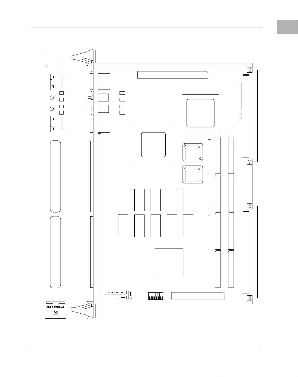
Figure 1-1 illustrates the placement of the switches, jumper headers,
connectors, and LED indicators on the MVME240x. Manually
configurable items on the MVME240x include:
❏ Flash memory bank A/bank B reset vector (J8)
❏ VMEbus system controller selection header (J9)
❏ General-purpose software-readable header (S3)
The MVME240x has been factory tested and is shipped with the
configurations described in the following sections. The MVME240x
factory-installed debug monitor, PPCBug, operates with those factory
settings.
1-8 Computer Group Literature Center Web Site
Page 25
DEBUG
MVME
240X
Preparing the MVME240x Hardware
1
189 190
DEBUG
PORT
J2
J1
12
A1B1C1
D1
ABT
RST
10/100 BASET
PCI MEZZANINE CARD PCI MEZZANINE CARD
BFL
CPU
PMC
ABORT
RESET
ETHERNET
PORT
U19
DS
1
DS
2
DS
3
DS
4
U9
FLASH SOCKETS
U22U17
U21U16
U20U15
U25
U23U18
U10
1
1
264
XU1 XU2
PMC 2 PMC1
63
1
63
1
63
1
J22
J21
63
1
264
J24
J23
63
1
264
J12
J11
63
1
264
J14
J13
P1
264
A32
B32
C32
264
A1B1C1
264
VME BUS
P2
264
SWITCH
S1 S2
SWITCH
J3
63
J5
1
2427 9812
3
8
J9
3
1
J8
S3
1
1 2 3 4 5 6 7 8
113 114
63
J6
12
D32D1D32
C32
B32
A32
Figure 1-1. MVME240x Switches, LEDs, Headers, Connectors
http://www.mcg.mot.com/literature 1-9
Page 26

1
Preparing and Installing the MVME2400-Series Module
Setting the Flash Memory Bank A/Bank B Reset Vector Header (J8)
Bank B consists of 1 MB of 8-bit Flash memory in two 32-pin PLCC 8-bi t
sockets.
Bank A consists of four 16-bit devices that are populated with 16Mbit
Flash devices (8 MB). A j umper header, J8, associ ated with the f irst set of
four Flash devices provides a total of 64KB of hardware-protected boot
block. Only 32-bit wri tes are sup ported for thi s bank of Fla sh. The address
of the reset vector is jumper-selectable. A jumper must be inst al le d ei the r
between J8 pins 1 and 2 for Bank A factory configuration, or between J8
pins 2 and 3 for Bank B. When the jumper is installed, the SMC (System
Memory Controller) of the Hawk ASIC maps 0xFFF00100 to the Bank B
sockets..
J8
1
2
3
Bank A (factory configuration)
J8
1
2
3
Bank B
Setting the VMEbus System Controller Selection Header (J9)
The MVME240x is factory-configured in automatic sy stem controller
mode; i.e., a jumper is installed across pins 2 and 3 of header J9. This
means that the MVME240x determi nes if it is system co ntr oller at sys tem
power-up or reset by its position on the bus; if it is in slot 1 on the VME
system, it configures itself as the system controller.
Remove the jumper from J9 if you intend to operate the MVME240x as
system controller in all cases.
Install the jumper across pins 1 and 2 if the MVME240x is not to operate
as system controller under any circumstances.
1-10 Computer Group Literature Center Web Site
Page 27

Preparing the MVME240x Hardware
1
J9
1
2
3
Automatic System Controller
(factory configuration)
System Controller Enabled
J9
1
2
3
System Controller Disabled
J9
1
2
3
Setting the General-Purpose Software-Readable Header (SRH) Switch(S3)
Switch S3 is an eight pole single-throw switch with softwa re readable
switch settings. These settings can be read as a register at ISA I/O address
$801 (hexadecimal). Each switch pole can be set to either logic 0 or l ogic
1. A logic 0 means th e switch is in the “ON” position for that particula r bit.
A logic 1 means the switch is i n the “OFF” positi on for t hat par ticu lar bit.
SRH Register Bit 0 is associated with Pin 1 and Pin 16 of the SRH, and
SRH Register Bit 7 i s associated with Pin 8 and Pin 9 of the SRH. The SRH
is a read-only register.
If Motorola’s PowerPC firmware, PPCBug, is being used, it reserves all
bits, SRH0 to SRH7. If it is not being used, the switch can be used for other
applications.
1
12345678
16 16
ON ON
SRH0 = 0
SRH1 = 0
SRH2 = 0
SRH3 = 0
SRH4 = 0
SRH5 = 0
SRH6 = 0
SRH7 = 0
1
12345678
SRH0 = 1
SRH1 = 1
SRH2 = 1
SRH3 = 1
SRH4 = 1
SRH5 = 1
SRH6 = 1
SRH7 = 1
Figure 1-2. General-Purpose Software-Readable Header
http://www.mcg.mot.com/literature 1-11
Page 28

1
Preparing and Installing the MVME2400-Series Module
PMCs
For a discussion of any configurable it ems on the PMCs, refer to the user’s
manual for the particular PMCs.
PMCspan
You will need to use an additional slot in the VME chassis for each
PMCspan expansion module you plan to us e. Before installing a PMCspan
on the MVME240x, you must install t he selecte d PMCs on the PMCspan.
Refer to the PMCspan PMCAdapter Carrier Module Instllation and Use
manual for instructions.
System Console Terminal
Ensure that the switc hes are set in the proper positi on for all bits on switch
S3 of the MVME240x board as shown in Figure 1-2. This is necessary
when the PPCBug firmware is used. Connect the ter minal via a cable to th e
RJ45 DEBUG connector J2. See Table C- 3 for pin sign al assignment s. Set
up the terminal as follows:
– Eight bits per character
– One stop bit per character
– Parity disabled (no parity)
– Baud rate = 9600 baud (default baud rate of the port at power-
up); after power-up, you can reconfigure the baud rate with
PPCBug’s PF command
1-12 Computer Group Literature Center Web Site
Page 29

Installing the MVME240x Hardware
Installing the MVME240x Hardware
The following paragraphs discuss installing PMCs onto the MVME240x,
installing PMCspan modules onto the MVME240x, installing the
MVME240x into a VME chassis, and connecting an optional system
console terminal.
ESD Precautions
Motorola strongly recommends that you use an a ntistatic wrist stra p and a
conductive foam pad when installing or upgrading a system. Electronic
components, such as d isk dr ives, c omputer boards , and memor y modules ,
can be extremely sensitive to Electro-Static Discharge (ESD). After
removing the component fr om th e system or its protective wrapper, place
the component flat o n a grounded, static-free surface (and in the case of a
board, component side up). Do not slide the component over any surface.
If an ESD station is not available, you can avoid damage resulting from
ESD by wearing an antistatic wrist strap (available at electronics stores)
that is attached to an unpainted metal part of the system chassis.
1
PMCs
PCI mezzanine card (PMC) modules mount on top of the MVME240x
module, and/or on a PMCspan. Refer to Figure 1-3 and perform the
following steps to install a PMC on your MVME240x module. This
procedure assumes that you have read the user’s manual that came with
your PMCs.
1. Attach an ESD strap to your wrist . Attach the othe r end of t he ESD
strap to the chassis as a ground. The ESD strap must be secured to
your wrist and to ground throughout the procedure.
2. Perform an operating system shutdown. Turn the AC or DC power
off and remove the AC cord or DC power lines from the system.
Remove chassis or system cover(s) as necessary for access to the
VMEmodules.
http://www.mcg.mot.com/literature 1-13
Page 30

1
Preparing and Installing the MVME2400-Series Module
Inserting or removin g modules with power applied may re sult
!
Caution
!
Warning
!
Caution
in damage to module components.
Dangerous voltages, capable of causing death, are present in
this equipment. Use extreme caution when handling, testing,
and adjusting.
3. If the MVME240x has a lready been installed i n a VMEbus card slot,
carefully remove it. Lay the MVME240x flat, with connectors P1
and P2 facing you.
Avoid touching areas of integrated circuitry; static discharge
can damage these circuits.
4. Remove the PCI filler plate from the selec ted PM C slot in t he fron t
panel of the MVME240x. If inst alling a double-width PMC, remove
the filler plates from b oth PMC slots.
1-14 Computer Group Literature Center Web Site
Page 31

Installing the MVME240x Hardware
2064 9708
1
Figure 1-3. Typical Single-width PMC Module Placement on MVME240x
5. Slide the edge connect or(s) of t he PMC module into t he front pane l
opening(s) from behind and place the PMC module on top of the
MVME240x. The four connectors on the underside of the PMC
module should then connect smoothly with the corresponding
connectors for a single-width PMC (J11/J12/J13/J14 or
J21/J22/J23/J24, all eight for a double-width PMC) on the
MVME240x.
6. Insert the two shor t Phillips scr ews through the hol es at the forwa rd
corners of the PMC module, i nto t he st andoff s on t he MVME240x.
Tighten the screws.
7. If installing two si ngle-width PMCs, repeat the above procedure for
the second PMC.
http://www.mcg.mot.com/literature 1-15
Page 32

1
Preparing and Installing the MVME2400-Series Module
Primary PMCspan
To install a PMCspan-002 PCI expansion module on your MVME240x,
refer to Figure 1-4 and perform the following steps. This procedure
assumes that you have read the user’s manual that was furnished with the
PMCspan, and that you have i nstalled the selected PMCs on the PMCspan
according to the instructions given in the PMCspan and PMC manuals.
1. Attach an ESD strap to your wrist . Attach the othe r end of t he ESD
strap to the chassis as a ground. The ESD strap must be secured to
your wrist and to ground while you are performing the installation
procedure.
2. Perform an operating system shutdown. Turn the AC or DC power
off and remove the AC cord or DC power lines from the system.
Remove chassis or system cover(s) as necessary for access to the
VME module card cage.
Inserting or removin g modules with power applied may re sult
!
Caution
in damage to module components.
Dangerous voltages, capable of causing death, are present in
!
Warning
!
Caution
1-16 Computer Group Literature Center Web Site
this equipment. Use extreme caution when handling, testing,
and adjusting.
3. If the MVME240x has already been installed in the chassis,
carefully remove it from the VMEbus card slot and lay it flat, with
connectors P1 and P2 facing you.
Avoid touching areas of integrated circuitry; static discharge
can damage these circuits.
Page 33

P4
Installing the MVME240x Hardware
1
J6
2081 9708
Figure 1-4. PMCspan-002 Installation on an MVME240x
http://www.mcg.mot.com/literature 1-17
Page 34

1
Preparing and Installing the MVME2400-Series Module
4. Attach the four standoffs to the MVME240x module. For each
standoff:
– Insert the threaded end into the standoff hole at each corner of
the VME processor module.
– Thread the locking nuts onto the standoff tips.
– Tighten the nuts with a box- end wrenc h or a pair of needl e nose
pliers.
5. Place the PMCspan on top of the MVME240x module. Align the
mounting holes in each corner to the standoff s, and align PMCspan
connector P4 with MVME240x connector J6.
6. Gently press the PMCs pan an d MVME240 x tog et her , ma kin g sur e
that P4 is fully seated i nto J6.
7. Insert the f our short Phillip s screws t hrough the holes at the c orners
of the PMCspan and into the standoffs on the MVME240x module.
Tighten the screws.
Note The screws have two different head diameters. Use the
screws with the smaller heads on the standoffs next to
VMEbus connectors P1 and P2.
Secondary PMCspan
The PMCspan-010 PCI expansion module mounts on top of a PMCspan002 PCI expansion module. To install a PMCspan-010 on your
MVME240x, refer to Figure 1-5 and perform the following steps. This
procedure assumes that you have re ad the user’s man ual that was f urnished
with the PMCspan, and that you have installed the selected PMCs on the
PMCspan according to the instructions given in the PMCspan and PMC
manuals.
1. Attach an ESD strap to your wrist . Attach the othe r end of t he ESD
strap to the chassis as a ground. The ESD strap must be secured to
your wrist and to ground while you are performing the installation
procedure.
1-18 Computer Group Literature Center Web Site
Page 35

Installing the MVME240x Hardware
P3
1
J3
2065 9708
Figure 1-5. PMCspan-010 Installation onto a PMCspan-002/MVME240x
http://www.mcg.mot.com/literature 1-19
Page 36

1
Preparing and Installing the MVME2400-Series Module
2. Perform an operating system shutdown. Turn the AC or DC power
off and remove the AC cord or DC power lines from the system.
Remove chassis or system cover(s) as necessary for access to the
VME module card cage.
Inserting or removin g modules with power applied may re sult
!
Caution
!
Warning
!
Caution
in damage to module components.
Dangerous voltages, capable of causing death, are present in
this equipment. Use extreme caution when handling, testing,
and adjusting.
3. If the Primary PMC Carrier Module/MVME240x assembly is
already installed in the VME chassis, carefully remove the twoboard assembly fro m the VMEbus card slo ts and lay it fl at, with the
P1 and P2 connectors facing you.
Avoid touching areas of integrated circuitry; static discharge
can damage these circuits.
4. Remove the four short Phillips screws from the standoffs in each
corner of the primary PCI expansion module,
PMCspan-002.
5. Attach the four standoffs to the PMCspan-002.
6. Place the PMCspan-010 on top of the PMCspan-002. Align the
mounting holes in each corner to the standoffs, an d align PMCspan010 connector P3 with PMCspan-002 connector J3.
7. Gently press the two PMCspan modules togethe r, making sur e that
P3 is fully seated in J3.
8. Insert the f our short Phillip s screws t hrough the holes at the c orners
of PMCspan-010 and into the standoffs on the primary PMCspan-
002. Tighten the screws.
Note The screws have two different head diameters. Use the
screws with the smaller heads on the standoffs next to
VMEbus connectors P1 and P2.
1-20 Computer Group Literature Center Web Site
Page 37

Installing the MVME240x Hardware
1
MVME240
!
Caution
!
Warning
x
Before installing the MVME24 0x into your VM E chassis, ensure that the
jumpers on the MVME240x J8, J9, and S3 switch are configur ed, as
previously described. This procedure assumes that you have already
installed the PMCspan( s) if de sired, and any PMCs th at you have selecte d.
Proceed as fo llows to inst all the MVME240x in the VME chassis:
1. Attach an ESD strap to your wrist . Attach the othe r end of t he ESD
strap to the chassis as a ground. The ESD strap must be secured to
your wrist and to ground throughout the procedure.
2. Perform an operating system shutdown:
a. Turn the AC or DC power off and remove the AC cord or DC
power lines from the system.
Inserting or removin g modules with power app lied may result
in damage to module components.
Dangerous voltages, capable of causing death, are present in
this equipment. Use extreme caution when handling, testing,
and adjusting.
b. Remove cha ssis or system cover(s) as necessary for access to t he
VMEmodules.
3. Remove the filler panel from the card slot where you are going to
install the MVME2 40x. If you have inst alled one or more PMCspan
PCI expansion modules onto your MVME240x, you will need to
remove filler panels from one additional card slot for each
PMCspan, above the card slot for the MVME240x.
http://www.mcg.mot.com/literature 1-21
Page 38

1
Preparing and Installing the MVME2400-Series Module
– If you intend to use the MVME240 x as system controller, it must
occupy the leftmost card slot (slot 1). The system controller must
be in slot 1 to correctly in it iat e the bus-grant daisy-chain and to
ensure proper operation of the IACK daisy-chain driver.
– If you do not intend to use the MVME240x a s system contr oller,
it can occupy any unused card slot.
Avoid touching areas of integrated circuitry; static discharge
!
Caution
can damage these circuits.
4. Slide the MVME24 0x (and PMCspans if used) into the selected card
slot(s). Be sure t he m odule or modules is/ are seated properly in the
P1 and P2 connectors on the backplane. Do not damage or bend
connector pins.
5. Secure the MVME240x (and PMCspans i f used) i n the cha ssis wit h
the screws provided, making good contact with the transverse
mounting rails to minimize RF emissions.
Note Some VME backplanes (e.g., those used in Motorola
“Modular Chassis” syst ems) have a n auto-j umpering fe ature
for automatic propag ation of the IACK and BG s ignals. Step
6 does not apply to such backplane designs.
6. On the chassis backplane, remove the
(IACK) and
slot occupied by the MVME240x.
7. If you intend to use PPCBug interacti vely, connect the termin al that
is to be used as the PPCBug system console to the
the front panel of the MVME240x.
In normal operation the host CPU controls MVME240x operation
via the VME bus Universe registers.
1-22 Computer Group Literature Center Web Site
BUS GRANT (BG) jumpers from the header for t he card
INTERRUPT ACKNOWLEDGE
DEBUG port on
Page 39

Installing the MVME240x Hardware
8. Replace the chassis or system cover(s), cable peripherals to the
panel connectors as a ppr opriate, reconnect the s yst em t o the AC or
DC power source, and turn the equipment power on.
1
9. The MVME240x’s green
confidence tests is run, and the debugger prompt
appears.
Installation Considerations
The MVME240x draws power from the VMEbus backpla ne connectors P1
and P2. P2 is also used for the upper 16 bits o f data in 3 2-bit tr ansfers , and
for the upper 8 address lines in extended addressing mode. The
MVME240x may not function properl y wi tho ut its main board connected
to VMEbus backplane connectors P1 and P2.
Whether the MVME240x operates as a VMEbus master or as a VMEbus
slave, it is c onfigured for 3 2 bits of addr ess and 32 bits of dat a (A32/D3 2).
However, it handles A1 6 or A24 devi ces in the address ran ges indicat ed in
Chapter 4. D8 and/or D16 devices in the system must be handled by the
PowerPC processor software. Refer to the memory maps in Chapter 4.
The MVME240x contains shared onboard DRAM whose base address is
software-selectable. Both the onboard processor and off-board VMEbus
devices see this local DRAM at base physical address $00000000, as
programmed by the PPCBug fi rmware. This may be ch anged v ia software
to any other base address. Refer to the MVME240x programmer's
reference guide for more information.
If the MVME240 x tries to access off-board resources in a nonexistent
location and is not system controller, and if the system does not have a
global bus timeout, the MVME240x waits forever for the VMEbus cycle
to complete. This will cause the system to lock up. There is only one
situation in which th e syste m might lack th is gl obal bus timeou t: when t he
MVME240x is not the system cont roller and ther e is no global bus timeout
elsewhere in the system.
Multiple MVME240x boards may be installed in a single VME chassis.
Each must have a unique Universe address, selected by setting jumper s on
its J17 header, as described in Preparing the MVME240x. In general,
hardware multiprocessor features are supported.
CPU LED indicates activity as a set of
PPC1-Bug>
http://www.mcg.mot.com/literature 1-23
Page 40

1
Preparing and Installing the MVME2400-Series Module
Other MPUs on the VMEbus can interrupt, disable, communicate with,
and determine the opera tional status of the proc essor(s). One registe r of the
Universe set incl udes four bits that function as location monitors to all ow
one MVME240x processor to broadcast a sign al to any other MVM E240x
processors. All eight registers are accessible from any local processor as
well as from the V MEbus.
1-24 Computer Group Literature Center Web Site
Page 41

2Operating Instructions
Introduction
This chapter provides information about powering up the MVME240x
system, and functionality of the switches, status indicators, and I/O ports
on the front panels of the MVME240x and PMCspan modules.
Applying Power
After you have verified that all necessary hardware preparation has been
done, that all connections have been made correctly, and that the
installation is complete, you can power up the system. The MPU,
hardware, and firm ware initializa tion process is perf ormed by the PPCBug
firmware power-up or system reset. The fi rmware initializes t he devices on
the MVME240x module in preparation for booting the operating system.
The firmware is shipped from the factory with an appropriate set of
defaults. In most cases the re is no need to modify the firmware
configuration bef ore you boot the opera ting syste m. Refer to Chapter 6 f or
further information about modifying defaults.
2
The following flowchart shows the basic initialization process that takes
place during MVME240x system start-ups.
For further information on PPCbug, refer to Chapter 5, PPCBug; to
Appendix D, Troubleshooting the MVME240x; or to the PPCBug
documentation listed in Appendix A.
2-1
Page 42

Operating Instructions
2
STARTUP
INITIALIZATION
POST
BOOTING
MONITOR
Power-up/reset initialization
Initialize devices on the MVME240x
module/system
Power On Self Test diagnostics
Firmware-configured boot mechanism,
if so configured. Default is no boot.
Interactive, command-driven on-line PowerPC
debugger, when terminal connected.
MVME240
x
The front panel of the MVME240x module is shown on a following page.
Switches
There are two switches (ABT and RST) and four LED (l ight-emitting diode)
status indicators (
panel.
2-2 Computer Group Literature Center Web Site
BFL, CPU, PMC (two)) located on the MVME240x front
Page 43

MVME240x
ABT (S1)
RST (S2)
When activated by software, the Abort switch,
ABT, can generate an
interrupt signal from the base board to the processor at a userprogrammable level. The interrupt is normally used to abort program
execution and return control to the debugger firmware located in the
MVME240x Flash memory. The interrupt signal reaches the processor
module via ISA bus interrup t line IRQ8
∗. The signal is also available from
the general purpose I/O port, which allows software to pol l the Abort switch after
an IRQ8* interrupt and verify that it has been pressed.
The interrupter connect ed to the
ABT switch is an edge-sensitive circuit,
filtered to remove switch bounce.
The Reset switch,
be asserted in the MPC603 or MPC604. It also drives a
RST, resets all onboard devices and cau ses HRESET* to
SYSRESET*
signal if the MVME240x VME proce ssor modu le i s the syst em co ntroller .
The Universe ASIC includes bot h a global and a loca l rese t drive r. When
the Universe operates as the VMEbus system controller, the reset driver
provides a global system reset by asserting the VMEbus signal
SYSRESET*. A SYSRESET* signal may be generated by the RESET
switch, a power-up reset, a watchdog timeout, or by a control bit in the
Miscellaneous Control Register (MISC_CTL) in the Universe ASIC.
SYSRESET* remains asserted for at least 200 ms, as required by the
VMEbus specification.
2
Similarly, the Universe ASIC sup pli es an inpu t si gnal and a control bit to
initiate a local reset oper ation. By sett ing a control bit, software can
maintain a board in a reset state, disabling a faulty board from participating
in normal system operation. The local reset driver is enabled even when
the Universe ASIC i s not syst em controll er. Local rese ts may be g enerated
by the
RST switch, a power-up reset, a watchdog timeout, a VMEbus
SYSRESET*, or a control bit in the MISC_CTL register.
http://www.mcg.mot.com/literature 2-3
Page 44

Operating Instructions
2
Status Indicators
There are four LED (light-emitting diode) status
indicators located on the MVME240x front panel.:
CPU
, PMC2, and PMC1.
BFL (DS1)
The yellow
the BRDFAIL* signal line is active.
BFL,
BFL LED indicates board f ai lu re; l ig hts whe n
MVME
DEBUG
ABT
RST
10/100 BASET
240x
BFL
CPU
PMC
CPU (DS2)
The green
CPU LED indicates CPU activity; lights when
the DBB* (Data Bus Busy) signal line on the processor
bus is active.
PMC2 (DS3)
The top green
PMC LED indicates PCI activity; lights
PCI MEZZANINE CARD PCI MEZZANINE CARD
when the PCI bus grant to PMC2 signal line on the PCI
bus is active. This ind icates that a PMC installed on slot 2
is active.
PMC1 (DS4)
The bottom green
PMC LED indicates PCI activity; lights
when the PCI bus grant to PMC1 signal line on the PCI
bus is active. This ind icates that a PMC installed on slot 1
is active.
10/100 BASET Port
The RJ45 port on the front panel of the MVME240x
labeled
10BaseT/100Base TX interf ace, implemented with a DEC
21140/21143 device.
2-4 Computer Group Literature Center Web Site
10/100 BASET supplies the Ethernet LAN
Page 45

MVME240x
DEBUG Port
The RJ45 port labeled DEBUG on the front panel of the MVME240x
supplies the MVME240x serial communications interface, implemented
via a UART PC16550 controller chip from National Semiconductor. It is
asynchronous only. This se ri al port is configured for EIA-232- D DT E, as
shown in Figure 2-1.
The
to serve as the firmware console for the factory installed debugger,
PPCBug. The port is configured as follows:
After power-up, the baud rate of the
using the debugger’s Port Format (PF) command . Refer to Chapters 5 and
6 for information about PPCBug.
2
DEBUG port may be used for connect ing a terminal to the MVME2 40x
❏ 8 bits per character
❏ 1 stop bit per character
❏ Parity disabled (no parity)
❏ Baud rate = 9600 baud (default baud rate at power-up)
DEBUG port can be reconfigured by
http://www.mcg.mot.com/literature 2-5
Page 46

Operating Instructions
2
SOUT
RTS*
DTR*
SIN
CTS*
DCD*
PC16550
MVME240x
4
2
8
5
7
1
3
6
Debug
RJ45
Figure 2-1. MVME240x DEBUG Port Configuration
2-6 Computer Group Literature Center Web Site
Page 47

MVME240x
PMC Slots
Two openings located on the front panel provide I/O
expansion by allowing access to one or two 4-port singlewide or one 8-port double-wide PCI Mezzanine Card
(PMC), connected to the PMC connectors on the
MVME240x. For pin assignments f or the PMC connect ors,
refer to Appendix C.
Do not attempt to instal l any PMC boards without performing
!
Warning
PCI MEZZANINE CARD (PMC Slot 1)
an operating system shutdown and following the procedures
given in the user’s manual for the particular PMC.
The right-most (lower) opening labeled
CARD on the MVME240x front panel provides front panel
I/O access to a PMC that is connected to the 64-pin
connectors J11 through J14 on the MVME240x module.
Connector J14 allows rear panel P2 I/O.
This slot is MVME240x Port 1.
PCI MEZZANINE
2
PMC2
PMC1
PCI MEZZANINE CARD PCI MEZZANINE CARD
PCI MEZZANINE CARD (PMC Slot 2)
The left-most (upper)opening labeled
CARD
on the MVME240x front panel prov ides front panel
PCI MEZZANINE
I/O access to a PMC that is connected to the 64-pin
connectors J21 through J24 on the MVME240x module.
Connector J24 allows rear panel P2 I/O.
This slot is MVME240x Port 2.
http://www.mcg.mot.com/literature 2-7
Page 48

Operating Instructions
2
PMCspan
A PMCspan front panel is pictured on the previous page. The front panel
is the same for all PMCspan models.
There are two PMC slots, labeled
either two single-wide PMCs or one double-wide PMC.
The PMCspan board has two sets of three 32-bit connectors for PMC
interface to a secondary PCI bus and a user-specific I/O. It also has a P1
connector and a 5-row P2 connector for power and VMEbus I/O.
The PMCspan has two green LEDs on its front panel, one for each PMC
slot, labeled
individual LED is illuminated whenever a PMC has been granted bus
mastership of the secondary PCI bus.
The right-most (l ower) opening l abeled
panel is Port 1.
The left-most (upper)opening labeled
panel is Port 2.
PCI MEZZANINE CARD, which support
PMC2 and PMC1. Both LEDs are illuminated du ring rese t. An
PCI MEZZANINE CARD on the front
PCI MEZZANINE CARD on the front
2-8 Computer Group Literature Center Web Site
Page 49

3Functional Description
Introduction
This chapter descr ibes the MVME240x VME process or module on a block
diagram level. The General Description provides an overview of the
MVME240x, followed by a detailed description of several blocks of
circuitry. Figure 3-1 shows a block diagram of the overall board
architecture.
Detailed descriptions of other MVME240x blocks, including
programmable registe rs in the ASICs and peripheral c hips, can be f ound in
the MVME2400-Series VME Processor Module Programmer’s Reference
Guide (part number V2400A/PG). Refer to it for a functional description
of the MVME240x in greater depth.
Features
3
The following table summarizes the features of the MVME240x VME
processor module.
Table 3-1. MVME240x Features
Feature Description
233 MHZ MPC750 PowerPC
Microprocessor
Form factor 6U VMEbus
SDRAM
L2 Cache
(MVME2401 - 2402 models)
350 MHZ MPC750 PowerPC
(MVME2431 - 2434 models)
Double-Bit-Error detect, Single-Bit-Error correct across 72 bits 32MB,
64MB, or 128MB SDRAM
Build-option for 1MB back side L2 Cache using l ate write or burstmode SRAMS
TM
processor
TM
processor
3-1
Page 50

Functional Descr iption
Feature Description
Table 3-1. MVME240x Features (Continued)
3
Flash memory
Memory Controller Hawk’s SMC (System Memory Controller)
PCI Host Bridge Hawk’s PHB (PCI Host Bridge)
Interrupt Controller Hawk’s MPIC (Multi-Processor Interrupt Controller)
PCI Interface 32/64-bit Data, 33MHz operation
Real-time clock
Peripheral Support
Switches Reset
Status LEDs Four: Board fail (BFL), CPU, PMC (one for PMC slot 2, one for slot 1)
Timers
VME I/O VMEbus P2 connector
PCI interface
Sockets for 1 MB
8 MB Soldered on-board
8KB NVRAM with RTC and battery backup (SGS-Thomson
M48T559)
One 16550-compatible async serial port routed to front panel RJ45
10BaseT/100BaseTX Ethernet interface routed to front panel RJ45
(RST) and Abort (ABT)
One 16-bit timer in W83C553 ISA bridge; four 32-bit timers in MPIC
device
Watchdog timer provided in SGS-Thomson M48T59
Two IEEE P1386.1 PCI Mezzanine Card (PMC) slots for one doublewidth or two single-width PMCs
Front panel and/or VMEbus P2 I/O on both PMC slots
One 114-pin Mi ct or conn ector for optional PMCspan expan sion module
3-2 Computer Group Literature Center Web Site
Page 51

Table 3-1. MVME240x Features (Continued)
Feature Description
Features
VMEbus interface
VMEbus system controller functions
64-bit PCI (Universe 2)
VMEbus-to-local-bus interface (A32/A24/A16, D64 (MBLT)
D32//D16/D08 Master and Slave
Local-bus-to-VMEbus interface (A16/A24/A32, D8/D16/D32)
VMEbus interrupter
VMEbus interrupt handler
Global Control/Status Register (GCSR) for interprocessor
communications
DMA for fast local memory/VMEbus transfers (A16/A24/A32,
D16/D32/D64)
3
http://www.mcg.mot.com/literature 3-3
Page 52

Functional Descr iption
General Description
The MVME240x is a VME processor module equipped with a PowerPC
3
604 RISC (MPC750) microprocessor.
As shown in the Features section, the MVME240x offers many standard
features desirable in a computer system—including Ethernet and debug
ports, Boot ROM, Flash memory, SDRAM, and interface for two PCI
Mezzanine Cards (PMCs), contained in a one-slot VME package. Its
flexible mezzani ne ar chite cture al lows r elat ively ea sy upgr ades o f the I/O.
There are four standard buses on the MVME240x:
PowerPC Processor Bus ISA Bus
PCI Local Bus VMEbus
As shown in Figure 3-1, the PCI Bridge portion of the Hawk ASIC
provides the interface from the Processor Bus to the PCI. A W83C553
PCI/ISA Bridge (PIB) Controller device performs the bridge function
between PCI and ISA. The Universe ASIC device provides the interface
between the PCI Local Bus and t he VMEbus. Part of the Hawk ASIC is the
ECC memory controller.
The Peripheral Component Interface (PCI ) local bus is a key feature. In
addition to the on-board local bus peripherals, the PCI bus supports an
industry-standard mezzanine interface, IEEE P1386.1 PMC (PCI
Mezzanine Card).
Block Diagram
Figure 3-1 is a block diagram of the MVME2400’s overall architecture.
MPC750 Processor
The MVME240x can be ordered with a PowerPC 750 pr ocessor c hip with
32MB to 128MB of ECC SDRAM, and up to 9MB of Flash memory.
3-4 Computer Group Literature Center Web Site
Page 53

Debug Connector
Block Diagram
SDRAM
L2 Cache
512KB
or 1M
Processor
MPC750
Clock
Generator
33MHz 32/64-bit PCI
Bus
Hawk ASIC
System Memory Controller (SMC)
100 MHz MPC604 Proc essor
Local Bus
2,64-bit PMC Slo t
Ethernet
DEC21143
RJ45
10/100TX
RJ45
serial port
TL16C550
UART
PIB
W83c553
ISA Bus
ISA
Registers
RTC/NVRAM/WD
MK48T559
32/64/128MB
FLASH
1MB to 9MB
System
Registers
and PCI Host Bridge (PHB)
VME Bridge
Universe
Buffers
PCI Expansion
3
Slot2
PMC FrontIO
SLot1
Front Panel
PMC Front IO
VME P2
VME P1
2067 9708
Figure 3-1. MVME240x Block Diagram
http://www.mcg.mot.com/literature 3-5
Page 54

Functional Descr iption
The PowerPC 750 is a 64-bit proc essor with 32 KB on-c hip caches (32KB
data cache and 32KB instruction cache).
The PHB bridge controll er por tion of the Hawk ASIC prov ides t he bri dge
3
between the PowerPC microprocessor bus and the PCI local bus.
Electrically, the Hawk is a 64-bit PCI co nnection. Four programmable ma p
decoders in each direction provide flexible addressing between the
PowerPC microprocessor bus and the PCI local bus.
The power requirements for the MVME240x are shown in Table 3-2.
Table 3-2. Power Requirements
Configuration +5V Power +12V and -12V Power
L2 Cache
233 or 350MHz 750 3.3A typical
4.0A maximum
The MVME2400 SBC utilizes a back-door L2 cache structure via the
MPC750 processor chip. The MCP 750’s L2 cache is implemente d with an
onchip 2-way set-associative tag memory and external direct-mapped
synchronous SRAMs for data storage. The external SRAMs are accessed
through a dedicated 72-bit wide (64 bits of data and 8 bits of parity) L2
cache port. The board i s populated wit h 1MB of L2 cache SRAMs. The L2
cache can operate in copyback or writethru modes and supports system
cache coherency throug h snooping. Parity generat ion and checking may be
disabled by programming the MCP750 accordingly. Refer to the
MVME2400 Programmer’s Reference Guide for additional information.
PMC-dependent
(Refer to Appendix B)
3-6 Computer Group Literature Center Web Site
Page 55

Block Diagram
Hawk System Memory Controller (SMC)/PCI Host Bridge (PHB) ASIC
The Hawk ASIC provides the bridge function between the MPC60x bus
and the PCI Local Bus. It provides 32-bit addressing and 64-b it dat a. The
64-bit addressing (dual address cycle) is not supported. The Hawk
supports various PowerPC processor external bus frequencies up to
100MHz.
There are four programmable map decoders for each direction to provide
flexible address mapp ings between the M PC and the PCI Local Bus. Re fer
to the MVME2400 Programmer’s Reference Guide for additional
information.
The Hawk ASIC also provides an MPIC Interrupt Controller to handle
various interrupt sources. The interrupt sources are: Four MPIC Timer
Interrupts, the interrupts from all PCI devices, the two software interrupts,
and the ISA interr upts. The ISA in terr upts a ctually ar e hand led a s a s ingle
8259 interrupt at INT0.
3
http://www.mcg.mot.com/literature 3-7
Page 56

Functional Descr iption
PCI Bus Latency
The following table lists the latency of PCI originated transactions for five
different clock ratios: 5:2, 3:2, 3:1, 2:1, and 1:1. The MVME2400 uses a
3
3:1 clock ratio:
Table 3-3. PCI Originated Latency Matrix
Transaction
Beat
32-bit PCI 64-bit PCI
Beat2Beat3Beat4Total Beat1Beat2Beat3Beat4Total
Clock
Ratio
1
Burst Read9111129111125:2
Burst Write3111631116
Single Read 9 - - - 9 9 - - - 9
Single Write 3 - - - 3 3 - - - 3
Burst Read 12 1 1 1 15 12 1 1 1 15 3:2
Burst Write3111631116
Single Read 12 - - - 12 12 - - - 12
Single Write 3 - - - 3 3 - - - 3
Burst Read9111129111123:1
Burst Write3111631116
Single Read 9 - - - 9 - - - - Single Write 3 - - - 3 - - - - Burst Read111111411111142:1
Burst Write3111631116
Single Read 11 - - - 11 - - - - Single Write 3 - - - 3 - - - - Burst Read 16 1 1 1 19 16 1 1 1 19 1:1
Burst Write3111631116
Single Read 16 - - - 16 - - - - Single Write 3 - - - 3 - - - - -
3-8 Computer Group Literature Center Web Site
Page 57

Table 3-4. PCI Originated Bandwidth Matrix
Block Diagram
First 2
Transaction
64-bit Writes 10 213 18 237 26 246 4 266 5:2
64-bit Reads 16 133 24 178 32 200 4 266
32-bit Writes 18 118 34 125 50 128 8 133
32-bit Reads 24 89 40 107 5 6 114 8 133
64-bit Writes 10 427 18 474 26 492 4 533 3:2
64-bit Reads 19 225 27 316 37 346 4 533
32-bit Writes 18 237 34 251 50 256 8 267
32-bit Reads 28 152 44 194 60 213 8 267
64-bit Writes 10 213 18 237 26 246 4 266 3:1
64-bit Reads 16 133 24 178 32 200 4 266
32-bit Writes 18 118 34 125 50 128 8 133
32-bit Reads 24 89 40 107 5 6 114 8 133
64-bit Writes 10 213 18 237 26 246 4 266 2:1
64-bit Reads 18 118 26 164 34 188 4 266
32-bit Writes 18 118 34 125 50 128 8 133
32-bit Reads 26 82 42 102 5 8 110 8 133
64-bit Writes 10 427 18 474 30 427 5 427 1:1
64-bit Reads 23 186 34 251 46 278 5.5 388
32-bit Writes 18 237 34 251 50 256 8 267
32-bit Reads 31 138 47 182 63 203 8 267
Cache Lines
Clks
MBytes
sec
First 4
Cache Lines
Clks
MBytes
sec
First 6
Cache Lines
Clks
MBytes
sec
Continuous
Clks/
Line
MBytes
sec
Clock
Ratio
3
http://www.mcg.mot.com/literature 3-9
Page 58

Functional Descr iption
PPC Bus Latency
The following tables list the latency of PPC or iginated transact ions and the
bandwidth of originated transactions for five different clock ratios: 5:2,
3
3:2, 3:1, 2:1, and 1:1. The MVME2400 uses a 3:1 clock ratio:
Table 3-5. PPC60x Originated Latency Matrix
Transaction
Beat
32-bit PCI 64-bit PCI
Beat2Beat3Beat4Total Beat1Beat2Beat3Beat4Total
Clock
Ratio
1
Burst Read 40 1 1 1 43 29 1 1 1 32 5:2
Burst Write5111851118
Single Read 22 - - - 22 - - - - Single Write 5 - - - 5 - - - - Burst Read 26 1 1 1 29 20 1 1 1 23 3:2
Burst Write5111851118
Single Read 16 - - - 16 - - - - Single Write 5 - - - 5 - - - - Burst Read 45 1 1 1 48 33 1 1 1 36 3:1
Burst Write5111851118
Single Read 24 - - - 24 - - - - Single Write 5 - - - 5 - - - - Burst Read 33 1 1 1 36 25 1 1 1 28 2:1
Burst Write5111851118
Single Read 19 - - - 19 - - - - Single Write 5 - - - 5 - - - - Burst Read 20 1 1 1 23 16 1 1 1 19 1:1
Burst Write5111851118
Single Read 13 - - - 13 - - - - Single Write 5 - - - 5 - - - - -
3-10 Computer Group Literature Center Web Site
Page 59

Table 3-6. PPC60x Originated Bandwidth Matrix
Block Diagram
First 2
Transaction
64-bit Writes 14 381 58 184 108 148 25 107 5:2
64-bit Reads------32.582
32-bit Writes 14 381 78 137 148 108 35 76
32-bit Reads------42.563
64-bit Writes 14 457 38 337 68 282 15 213 3:2
64-bit Reads------22.5142
32-bit Writes 14 457 50 256 92 209 21 152
32-bit Reads------28.5112
64-bit Writes 14 457 67 191 127 151 30 107 3:1
64-bit Reads------3689
32-bit Writes 14 457 98 131 182 105 42 76
32-bit Reads------4867
64-bit Writes 14 305 48 178 88 145 20 107 2:1
64-bit Reads------2876
32-bit Writes 14 305 64 133 120 107 28 76
32-bit Reads------3659
64-bit Writes 14 305 29 294 49 261 10 213 1:1
64-bit Reads------18118
32-bit Writes 14 305 37 231 65 197 14 152
32-bit Reads------2297
Cache Lines
Clks
MBytes
Sec
First 4
Cache Lines
Clks
MBytes
Sec
First 6
Cache Lines
Clks
MBytes
Sec
Continuous
Clks/
Line
MBytes
Sec
Clock
Ratio
3
http://www.mcg.mot.com/literature 3-11
Page 60

Functional Descr iption
Table 3-7. PCI Originated Bandwidth Matrix
3
Transaction
64-bit Writes 10 213 18 237 26 246 4 266 5:2
64-bit Reads 16 133 24 178 32 200 4 266
32-bit Writes 18 118 34 125 50 128 8 133
32-bit Reads 24 89 40 107 5 6 114 8 133
64-bit Writes 10 427 18 474 26 492 4 533 3:2
64-bit Reads 19 225 27 316 37 346 4 533
32-bit Writes 18 237 34 251 50 256 8 267
32-bit Reads 28 152 44 194 60 213 8 267
64-bit Writes 10 213 18 237 26 246 4 266 3:1
64-bit Reads 16 133 24 178 32 200 4 266
32-bit Writes 18 118 34 125 50 128 8 133
32-bit Reads 24 89 40 107 5 6 114 8 133
64-bit Writes 10 213 18 237 26 246 4 266 2:1
64-bit Reads 18 118 26 164 34 188 4 266
32-bit Writes 18 118 34 125 50 128 8 133
32-bit Reads 26 82 42 102 5 8 110 8 133
64-bit Writes 10 427 18 474 30 427 5 427 1:1
64-bit Reads 23 186 34 251 46 278 5.5 388
32-bit Writes 18 237 34 251 50 256 8 267
32-bit Reads 31 138 47 182 63 203 8 267
First 2
Cache Lines
Clks
MBytes
sec
First 4
Cache Lines
Clks
MBytes
sec
First 6
Cache Lines
Clks
MBytes
sec
Continuous
Clks/
Line
MBytes
sec
Clock
Ratio
Assumptions
Certain assumptions have been made with regard to MVME2400
performance. Somethings which are assumed in making the
aforementioned tables include the following:
3-12 Computer Group Literature Center Web Site
Page 61

Clock Ratios and Operating Frequencies
Performance is based on the appropriate clock ratio and corresponding
operating frequency: ’
Table 3-8. Clock Ratios and Operating Frequencies
Block Diagram
3
Ratio
5:2 83 33 8
3:2 100 66 8
3:1 100 33 8
2:1 66 33 10
1:1 66 66 10
PPC60x Originated
❏ Count represents number of PPC60x bus clock cycles.
❏ Assumes write posting FIFO is initially empty.
❏ Does not include time taken to obtain grant for PPC60x bus. The
❏ PPC60x bus is idle at the time of the start of the transaction. (i.e., no
❏ Cache aligned transfer, not critical word first.
❏ PCI medium responder with no zero states.
❏ One clock request/one clock grant PCI arbitration.
PPC60x Clock
(MHz)
PCI Clock
(MHz)
SDRAM Speed
(ns)
count starts on the same clock period that TS_ is asserted.
pipelining effects).
❏ Write posting enabled.
❏ Default FIFO threshol d settings
❏ Single beat writes are aligned 32-bit transfer, always executed aws
32-bit PCI.
http://www.mcg.mot.com/literature 3-13
Page 62

Functional Descr iption
❏ Clock counts represent best case alignment between PCI and
PPC60x clock domains. An exception to this is continuous
bandwidth which reflects the average affects of clock alignment.
3
PCI Originated
❏ Count represents number of PCI Bus clock cycles.
❏ Assumes write posting FIFO is initially empty
❏ L2 caching is not en abled, all tran sactions exclus ively contro lled by
the SMC.
❏ Does not include time taken to obtai n grant for PCI Bus. The count
starts on the same clock period that FRAME_ is asserted.
❏ One clock request/one clock grant PPC60x bus arbitration.
❏ PPC60x bus traffic limited to PHB transactions only.
❏ Write posting and read adhead enabled.
❏ Default FIFO threshol d settings.
❏ One cache line = 32 bytes.
SDRAM Memory
The MVME2400 SDRAM memory size can be 32MB, 64MB, or 128MB.
The SDRAM blocks are controlled by the Hawk ASIC which provides
single-bit error correction and double-bit error detection. ECC is
calculated over 72-bits.
The memory block size is de pen dant upon the SDRAM devices installed.
Installing five 64Mbit (16bit data) devices provides 32MB of memory.
With 64Mbit (8bit data) devices, there are two blocks consisting of 9
devices each that total 64MB per block. In this case, either block can be
populated for 64Mbytes or 128 Mbytes of onboard memory. With 128Mbit
(8bit data) devices, the blocks can be populated for 128Mbytes and
256Mbytes. If 64Mbit (4bit data) devices are installed, there is one block
3-14 Computer Group Literature Center Web Site
Page 63

Block Diagram
consisting of 18 devices that total 128Mbytes. With 128Mbit (4bit data)
devices, the block contains 256Mbytes. When populated, these blocks
appear as Block A and Block B to the Hawk.
Refer to the MVME2400-Series VME Processor Module Programmer’s
Reference Guide for additional information and programming details.
SDRAM Latency
The following table shows the performance summary for SDRAM when
operating at 100MHz using PC100 SDRAM with a CAS_latency of 2. The
figure on the next page defines the times that are specified in the table.
Table 3-9. 60x Bus to SDRAM Access Timing (100MHz/PC100 SDRAMs)
ACCESS TYPE
4-Beat Read after idle,
SDRAM Bank Inactive
4-Beat Read after idle,
SDRAM Bank Active - Page Miss
4-Beat Read after idle,
SDRAM Bank Active - Page Hit
4-Beat Read after 4-Beat Read,
SDRAM Bank Active - Page Miss
Access Time
(tB1-tB2-tB3-tB4)
10-1-1-1
12-1-1-1
7-1-1-1
5-1-1-1
Comments
3
4-Beat Read after 4-Beat Read,
SDRAM Bank Active - Page Hit
4-Beat Write after idle,
SDRAM Bank Active or Inactive
4-Beat Write after 4-Beat Write,
SDRAM Bank Active - Page Miss
http://www.mcg.mot.com/literature 3-15
2.5-1-1-1 2.5-1-1-1 is an average of 21-1-1 half of the time and 31-1-1 the other half.
4-1-1-1
6-1-1-1
Page 64

Functional Descr iption
Table 3-9. 60x Bus to SDRAM Access Timing (100MHz/PC100 SDRAMs)
ACCESS TYPE
Access Time
(tB1-tB2-tB3-tB4)
Comments
3
4-Beat Write after 4-Beat Write,
SDRAM Bank Active - Page Hit
1-Beat Read after idle,
SDRAM Bank Inactive
1-Beat Read after idle,
SDRAM Bank Active - Page Miss
1-Beat Read after idle,
SDRAM Bank Active - Page Hit
1-Beat Read after 1-Beat Read,
SDRAM Bank Active - Page Miss
1-Beat Read after 1-Beat Read,
SDRAM Bank Active - Page Hit
1-Beat Write after idle,
SDRAM Bank Active or Inactive
3-1-1-1 3-1-1-1 for the second burst
write after idle.
2-1-1-1 for subsequent burst
writes.
10
12
7
8
5
5
1-Beat Write after 1-Beat Write,
SDRAM Bank Active - Page Miss
1-Beat Write after 1-Beat Write,
SDRAM Bank Active - Page Hit
3-16 Computer Group Literature Center Web Site
13
8
Page 65

Notes 1. SDRAM speed attributes are programmed for the
following: CAS_latency = 2, tRCD = 2 CLK Per iod s, t R P =
2 CLK Periods, tRAS = 5 CLK Periods, tRC = 7 CLK
Periods, tDP = 2 CLK Periods, and the swr_dpl bit is set in
the SDRAM Speed Attributes Register.
2. The Hawk is configured for “no external register s” on the
SDRAM control signals.
3. tB1, tB2, tB3, and tB4 are specifi ed in the following figure.
tB4
tB3
tB2
tB1(From Idle) tB1(Back-to-Back)
Block Diagram
3
Figure 3-2. Timing Definitions for PPC Bus to SDRAM Access
http://www.mcg.mot.com/literature 3-17
Page 66

Functional Descr iption
Notes When the initial bus state is idle, tB1 reflects the number of
CLK periods from the rising edge of the CLK that drives
TS_low, to th e rising edge of the CLK that samples the first
3
TA_low.
When the bus is busy and TS_ is being asserted as soon as
possible after Hawk asserts AACK_ the back-to-back
condition occurs. When back-to-back cycles occur, tB1
reflects the number of CLK periods from the rising edge of
the CLK that sa mples the last TA_ lo w of a data tenure t o the
rising edge of the CLK tha t samp les th e firs t TA_ l ow of the
next data tenure.
The tB2 function reflects the number of CLK periods from
the rising edge of the CLK that samples the first TA_ low in
a burst data ten ure to the rising edge of the CLK t hat samples
the second T A_ low in that data tenure.
The tB3 function reflects the number of CLK periods from
the rising edge of the CLK that sampl es the second TA_ lo w
in a burst data tenure to the rising edge of the C LK that
samples the third TA_ low in that data tenure.
The tB4 function reflects the number of CLK periods from
the rising edge of the CLK that sample s the th ird TA_ low in
a burst data ten ure to the rising edge of the CLK t hat samples
the last TA_ low in that data tenure.
3-18 Computer Group Literature Center Web Site
Page 67

Flash Memory
The MVME240x base board contain s two banks of FLASH memory. Bank
B consists of two 32-pin devices which can be populated with 1MB of
FLASH memory. Only 8-bit writes a re supported for this bank. Bank A has
four 16-bit Smart Vo ltage FLASH SMT devi ces. With the 16 Mbit FLASH
devices, the FLASH size is 8MB. A jumper header associated wit h the first
set of eight FLASH devices provides a total of 128 KB of hardwareprotected boot block. Only 32-bit writes are supported for this bank of
FLASH. There will be a jumper to tell the Hawk chip where to fetch the
reset vector. When the jumper is installed, the Hawk chip maps
0xFFF00100 to these sockets (Bank B).
The onboard monitor/debugger, PPCBug, resides in the Flash chips.
PPCBug provides functionality for:
Block Diagram
3
❏ Booting the system
❏ Initializing after a reset
❏ Displaying and modifying configuration variables
❏ Running self-tests and diagnostics
❏ Updating firmware ROM
Under normal operation, the Flash devices are in “read-only” mode, their
contents are pre-def ined, an d they are pr otected against i nadvert ent write s
due to loss of power conditions. However, for programming purposes,
programming voltage is always supplied to the devices and the Flash
contents may be modified by executing the proper program command
sequence. Refer to the PFLASH command in the PPCbug Debugging
Package User’s Manual for further device-specific info rmation on
modifying Flash contents.
ROM/Flash Performance
The SMC provides the interface for two blocks of ROM/Flash. Access
times to ROM/Flash are programmable for each block. Access times are
also affected by b lock width . The foll owing tabl es in t his subsect ion show
access times for ROM/Flash when configured for different device access
times.
http://www.mcg.mot.com/literature 3-19
Page 68

Functional Descr iption
Table 3-10. PPC Bus to ROM/Flash Access Timing (120ns @ 100MHz)
3
ACCESS TYPE
4-Beat Read 70 22 64 16 64 16 64 16 262 70
4-Beat Write N/A N/A
1-Beat Read (1 byte) 2222------2222
1-Beat Read (2 to 8 bytes)7022------7022
1-Beat Write 2121------2121
CLOCK PERIODS REQUIRED FOR:
1st Beat 2nd Beat 3rd Beat 4th Beat
16
Bits
64
Bits
16
Bits
64
Bits
16
Bits
64
Bits
16
Bits
64
Bits
Total
Clocks
16
Bits
64
Bits
Note: The information in Tabl e 3-10 is approp riat e when co nfi gured with
devices with an access time equal to 12 CLK periods.
Table 3-11. PPC Bus to ROM/Flash Access Timing (80ns @ 100MHz)
ACCESS TYPE
CLOCK PERIODS REQUIRED FOR:
1st Beat 2nd Beat 3rd Beat 4th Beat
16
Bits
64
Bits
16
Bits
64
Bits
16
Bits
64
Bits
16
Bits
64
Bits
Total
Clocks
16
Bits
64
Bits
4-Beat Read 54 18 48 12 48 12 48 12 198 54
4-Beat Write N/A N/A
1-Beat Read (1 byte) 1818------1818
1-Beat Read (2 to 8 bytes)5418------5418
1-Beat Write 2121------2121
Note: The information in Table 3 -11 is approp ri ate whe n confi gured wit h
devices with an access time equal to 8 CLK periods.
3-20 Computer Group Literature Center Web Site
Page 69

Block Diagram
Table 3-12. PPC Bus to ROM/Flash Access Timing (50ns @ 100MHz)
CLOCK PERIODS REQUIRED FOR:
ACCESS TYPE
4-Beat Read 42 15 36 9 36 9 36 9 150 42
4-Beat Write N/A N/A
1-Beat Read (1 byte) 1515------1515
1-Beat Read (2 to 8 bytes)4215------4215
1-Beat Write 2121------2121
1st Beat 2nd Beat 3rd Beat 4th Beat
16
64
16
64
16
64
16
Bits
Bits
Bits
Bits
Bits
Bits
Bits
64
Bits
Total
Clocks
16
Bits
64
Bits
Note: The information in Tabl e 3-12 is approp riat e when co nfi gured with
devices with an access time equal to 5 CLK periods.
Table 3-13. PPC Bus to ROM/Flash Access Timing (30ns @ 100MHz)
ACCESS TYPE
CLOCK PERIODS REQUIRED FOR:
1st Beat 2nd Beat 3rd Beat 4th Beat
16
64
16
64
16
64
16
Bits
Bits
Bits
Bits
Bits
Bits
Bits
64
Bits
Total
Clocks
16
Bits
64
Bits
3
4-Beat Read 34 13 28 7 28 7 28 7 118 34
4-Beat Write N/A N/A
1-Beat Read (1 byte) 1313------1313
1-Beat Read (2 to 8 bytes)3413------3413
1-Beat Write 2121------2121
Note: The information in Table 3 -13 is approp ri ate whe n confi gured wit h
devices with an access time equal to 3 CLK periods.
http://www.mcg.mot.com/literature 3-21
Page 70

Functional Descr iption
Ethernet Interface
The MVME240x module uses Digital Equipment’s DECchip 21143 PCI
3
Fast Ethernet LAN controller to implement an Ethernet interface that
supports 10Base-T/100Base-TX connections, via an RJ45 connector on
the front panel . The b al anced d iffe renti al t ra nsceiv er li nes a re coupl ed via
on-board transformers.
Every MVME240x is assigned an Ethe rnet stati on address. Th e address i s
$08003E2xxxxx, where xxxxx is the unique 5-nibble number assigned to
the board (i.e., every board has a different value for xxxxx).
Each MVME240x displays it s Ethernet station a ddress on a label at tached
to the base board in the PMC connec tor ke epout a rea jus t behi nd the fron t
panel. In addition, the six byt es incl udi ng th e Ethernet station address are
stored in the NVRAM (BBRAM) configuration area specified by boot
ROM. That is, the value 08003E2xxxxx is stored in NVRAM. The
MVME240x debugger, PPCBug, has the capa bility to retrieve the Etherne t
station add ress via the CNFG command.
Note The unique Ethernet address is set at the factory and should
not be changed. Any attempt to change this address may
create node or bus contention and thereby render the board
inoperable.
If the data in NVRAM is lost, use the number on the label in the PMC
connector keepout area to restore it.
For the pin assignments of the 10Base-T/100Base-TX connector, refer to
Appendix C.
At the physical layer, the Ethernet interface bandwidth is 10Mbit/second
for 10Base T. For the 100Base TX, it is 100Mbit/second. Refer to the
BBRAM/TOD Clock memory map description in the MVME2400-Series
VME Processor Module Programmer’s Reference Guide for detailed
programming information.
3-22 Computer Group Literature Center Web Site
Page 71

PCI Mezzanine Card (PMC) Interface
A key feature of the MVME240x fami ly is the PCI bus. In addit ion to the
on-board local bus devices (Ethernet, etc.), the PCI bus supports an
industry-standard mezzanine interface, IEEE P1386.1 PCI Mezzanine
Card (PMC).
PMC modules offer a variety of possibilities for I/O expansion such as
FDDI (Fiber Distributed Data Interface), ATM (Asynchronous Transfer
Mode), graphics, Ethernet, or SCSI ports. For a complete listing of
available PMCs, go to the GroupIPC WorldWideWeb site at URL
http://www.groupipc.com
panel and rear P2 I/ O. There is also provision for s tacking one or tw o PMC
carrier boards, or PMCspan PCI expansion modules, on the MVME240x
for additional expansi on.
The MVME240x supports two PMC slots. Two sets of four 64-pin
connectors on the base board (J11 - J14, and J21 - J24) interface with 32bit/64-bit IEEE P1386.1 PMC-compatible mezzanines to add any
desirable function.
/ . The MVME240x suppo rts PMC front
Block Diagram
3
Refer to Appendix C for the pin assignments of the PMC connectors. For
detailed programmi ng information, re fer to the PCI bus descriptio ns in the
MVME2400-Series VME Processor Module Programmer’s Reference
Guide and to the user documentation for the PMC modules you intend to
use.
PMC Slot 1 (Single-Width PMC)
PMC slot 1 has the following characteristics:
Mezzanine Type PCI Mezzanine Card (PMC)
Mezzanine Size
PMC Connectors J11 to J14 (32/64-Bit PCI with front and rear I/O)
Signaling Voltage V
http://www.mcg.mot.com/literature 3-23
S1B: Single width, standard depth (75mm x 150mm)
with front panel
= 5.0Vdc
io
Page 72

Functional Descr iption
For P2 I/O configurations, all I/O pins of PMC slot 1 are routed to the 5row power adapter c ard . Pins 1 through 64 of J14 are routed to r ow C and
row A of P2.
3
PMC Slot 2 (Single-Width PMC)
PMC slot 2 has the following characteristics:
Mezzanine Type PCI Mezzanine Card (PMC)
Mezzanine Size
PMC Connectors J21 to J24 (32/64-Bit PCI with front and rear I/O)
Signaling Voltage V
For P2 I/O configurations, 46 I/O pins of PMC slot 2 are routed to the 5row power adapter card. Pins 1 throu gh 46 of J24 are rou ted to r ow D and
row Z of P2.
PMC Slots 1 and 2 (Double-Width PMC)
PMC slots 1 and 2 with a double-width PMC have the following
characteristics:
S1B: Single width, standard depth (75mm x 150mm)
with front panel
= 5.0Vdc
io
Mezzanine Type PCI Mezzanine Card (PMC)
Mezzanine Size
PMC Connectors
Signaling Voltage V
Double width, standard depth (150mm x 150 mm)
with front panel
J11 to J14 and J21 to J24 (32/64-Bit PCI) with front
and rear I/O
= 5.0Vdc
io
PCI Expansion
The PMCspan expansion module connector, J6, is a 114-pin Mictor
connector. It is locat ed near P2 on the primary side of the MVME240x. Its
interrupt lines are routed to the MPIC.
3-24 Computer Group Literature Center Web Site
Page 73

VMEbus Interface
The VMEbus interface is implemented with the CA91C142 Universe
ASIC. The Universe chip interfaces the 32/64-bit PCI local bus to the
VMEbus.
The Universe ASIC provides:
❏ The PCI-bus-to-VMEbus interface
❏ The VMEbus-to-PCI-bus interface
❏ The DMA controller functions of the local VMEbus
The Universe chip includes Universe Control and Status Registers
(UCSRs) for interprocessor communications. It can provide the VMEbus
system controller functions as well. For detailed programming
information, refer to the Universe User’s Manual and to th e discussion s in
the MVME2400-Series VME Processor Module Programmer's Ref er enc e
Guide.
Maximum performance is achieved with D64 Multiplexed Block
Transfers (MBLT). The on-chip DMA channel should be used to move
large blocks of dat a to/ fr om t he VMEbu s. T he Un ive rs e s houl d be able to
reach 50MB/second in 64-bit MBLT mode.
Block Diagram
3
The MVME2400 interfaces t o the VMEbus via th e P1 and P2 connect ors,
which use the new 5-row 160-pin connectors as specified in the VME64
extension standard. It also draws +5V, +12V, and -12V power from the
VMEbus backplane through these two conn ectors. 3.3V and 2.5V supplies
are regulated onboard from the +5 power.
Asynchronous Debug Port
A Texas Instrument’s Universal Asynchronous Receiver/Transmitter
(UART) provides the asynchronous debug port. TTL-l evel si gnals fo r the
port are routed through appr opriate EIA-23 2-D drivers and recei vers to an
RJ45 connector on the fr ont panel. The e xternal sig nals are ESD pro tected.
http://www.mcg.mot.com/literature 3-25
Page 74

Functional Descr iption
For detailed programming information, refer to the MVME2400-Series
VME Processor Module Programmer’s Reference Guide and to Texas
Instrument’s data sheet #SLLS057D, dated August 1989, revised March
3
1996 for Asynchronous Communications Element (ACE) TL16C550A.
PCI-ISA Bridge (PIB) Controller
The MVME240x uses a Winbond W83C553 PCI/ISA Bridge (PIB)
Controller to supply the interface between the PCI local bus and the ISA
system I/O bus (diagrammed in Figure 3-1).
The PIB controller provides the following functions:
❏ PCI bus arbitration for:
– ISA (Industry Standard Architecture) bus DMA (not functional
on MVME240x)
– The PHB (PCI Host Bridge) MPU/local bus interface function,
implemented by the Hawk ASIC
– All on-board PCI dev i ces
– The PMC slot
❏ ISA bus arbitration for DMA devices
❏ ISA interrupt mapping for four PCI interrupts
❏ Interrupt controller functionality to support 14 ISA interrupts
❏ Edge/level control for ISA interrupts
❏ Seven independently programmable DMA channels
❏ One 16-bit timer
❏ Three interval counters/timers
Accesses to the configuration space for the PIB controller are performed
by way of the CONADD and CONDAT (Conf iguration Address and Data)
registers in the PHB. The regist ers are located at offsets $CF 8 and $CFC,
respectively, from the PCI I/O base address.
3-26 Computer Group Literature Center Web Site
Page 75

Real-Time Clock/NVRAM/Timer Function
The MVME240x employs an SGS-Thomson surface-mount M48T559
RAM and clock chip to provide 8KB of non-volatile static RAM, a realtime clock, and a watchdog timer function. This chip supplies a clock,
oscillator, crysta l, power fail ure detectio n, memory write pr otection , 8KB
of NVRAM, and a battery in a package consisting of two parts:
❏ A 28-pin 330mil SO device containing the real-time clock, the
oscillator, power failure detection circuitry, timer logic, 8KB of
static RAM, and gold-plated sockets for a battery
❏ A SNAPHAT battery housing a crystal along with the battery
The SNAPHAT battery package is mounted on top of the M48T559
device. The battery housing is keyed to prevent reverse insertion.
The clock furnishes seconds, minut es, hours, da y, date, month, and year in
BCD 24-hour format. Corrections for 28-, 29- (leap year), and 30-day
months are made automatically. The clock generates no interrupts.
Although the M48T559 is an 8-bit device, 8-, 16-, and 32-bit access es from
the ISA bus to the M48T559 are supported. Refer to the MVME2400-
Series VME Processor Module Programmer’s Reference Guide and to the
M48T559 data sheet for detailed programming and battery life
information.
Block Diagram
3
PCI Host Bridge (PHB)
The PHB portion of the Hawk ASIC pro vides the bridge f unction betwe en
the MPC60x bus and the PCI Local Bus. It provides 32 bit addressi ng and
64 bit data. The 64 bit a ddressing (dual addres s cycle) is not supported. Th e
Hawk supports various Po werPC pro cessor ex ternal bus f requenci es up to
100MHz and PCI frequencies up to 33MHz.
There are four programmable map decoders for each direction to provide
flexible address mapp ings between the M PC and the PCI Local Bus. Re fer
to the MVME2400-Series VME Processor Module Programmer’s
Reference Guide for additional information and programming details.
http://www.mcg.mot.com/literature 3-27
Page 76

Functional Descr iption
Interrupt Controller (MPIC)
The MPIC Interrupt Controller portion of the Hawk ASIC is designed to
3
handle various interrupt sources. The interrupt sources are:
❏ Four MPIC timer interrupts
❏ Processor 0 self interrupt
❏ Memory Error interrupt from the SMC
❏ Interrupts from all PCI devices
❏ Two software interrupts
❏ ISA interrupts (actually handles as a single 8259 interrupt at INT0)
Programmable Timers
Among the resources available to the local processor are a number of
programmable timers. Timers are incorporated into the PCI/ISA Bridge
(PIB) controller and the Hawk device (diagrammed in Figure 3-1). They
can be programmed to generate periodic interrupts to the processor.
Interval Timers
The PIB controller has three built-in counters that are equivalent to those
found in an 82C54 programmab le interval timer. The co unters are grouped
into one timer unit, Timer 1, in the PIB controller. Each counter output has
a specific function:
❏ Counter 0 is associated with interrupt request line IRQ0. It can be
used for system timing functions, such as a timer interrupt for a
time-of-day function.
❏ Counter 1 generates a refresh request signal for ISA memory. This
timer is not used in the MVME240x.
❏ Counter 2 provides the tone for the speaker output function on the
PIB controller (the
SPEAKER_OUT signal which can be cabled to an
external speaker via the remote reset connector). This fu nction is not
used on the MVME240x.
3-28 Computer Group Literature Center Web Site
Page 77

Block Diagram
The interval timers use the OSC clock input as their clock source. The
MVME240x drives the OSC pin with a 14.31818MHz clock source.
16/32-Bit Timers
There is one 16-bit timer and four 32-bit timers on the MVME240x. The
16-bit timer is pr ovided by the PIB. T he Hawk device provi des the four 32 bit timers that may be used for system timing or to generate periodic
interrupts. For information on programming these timers, refer to the data
sheet for the W83C553 PIB controll er and to the MVME2400-Ser ies VME
Processor Module Programmer’s Reference Guide.
3
http://www.mcg.mot.com/literature 3-29
Page 78

Functional Descr iption
3
3-30 Computer Group Literature Center Web Site
Page 79

4Programming the MVME240x
Introduction
This chapter provides basic information useful in programming the
MVME240x. This includes a description of memory maps, control and
status registers, PCI arbitration, interrupt handling, sources of reset, and
big/little endian issues.
For additional programming information about the MVME240x, refer to
the MVME2400-Series VME Processor Module Pro grammer’s Refe rence
Guide.
For programming information about the PMCs, refer to the applicable
user’s manual furnished with the PMCs.
Memory Maps
4
There are multiple buses on the MVME240x and each bus doma in h as it s
own view of the memory map. The following sections describe the
MVME240x memory organization from the following three points of
view:
❏ The mapping of all resourc es as vi ewed by t he MPU ( processo r bus
memory map)
❏ The mapping of onboard resources as viewed by PCI local bus
masters (PCI bus memory map)
❏ The mapping of onboard resources as viewed by VMEbus masters
(VMEbus memory map)
Additional, more detail ed memory maps can be found in the MVME2400 -
Series VME Processor Module Programmer’s Reference Guide.
4-1
Page 80

Programming the MVME240x
Processor Bus Memory Map
The processor memory map configur ation is und er the control of the PHB
and SMC portions of the Hawk ASI C. The Hawk adjusts sys tem mapping
to suit a given application via programmable map decoder registers. At
system power-up or reset, a default processor memory map takes over.
4
Default Processor Memory Map
The default processor memory map that is valid at power-up or reset
remains in effect until reprogrammed for specific applications. Table 4-1
defines the entire default map ($00000000 to $FFFFFFFF).
Table 4-1. Processor Default View of the Memory Map
Processor Address
Start End
00000000 7FFFFFFF 2GB Not Mapped
80000000 8001FFFF 128KB PCI/ISA I/O Space
80020000 FEF7FFFF 2GB-16MB-640KB Not Mapped
FEF80000 FEF8FFFF 64KB SMC Registers
FEF90000 FEFEFFFF 384KB Not Mapped
FEFF0000 FEFFFFFF 64KB PHB Registers
FF000000 FFEFFFFF 15MB Not Mapped
FFF00000 FFFFFFFF 1MB Flash Bank A or Bank B (See Note)
Size Definition
Notes
The first 1MB of Flash bank A (soldered Flash up to 8MB)
appears in this ran ge after a res et if the rom_b_rv control bit
in the SMC’s ROM B Base/Size register is cleared. If the
rom_b_rv contro l bit is s et, this add ress ran ge maps to Flas h
bank B (socketed 1MB Flash).
4-2 Computer Group Literature Center Web Site
Page 81

For detailed processor memory maps, including suggested CHRP- and
PREP-compatible memory maps, refer to the MVME2400-Series VME
Processor Module Programmer’s Reference Guide.
PCI Local Bus Memory Map
Memory Maps
The PCI memory map is control led by the MPU/PCI bus br idge controll er
portion of the Hawk ASIC and by the Universe PCI/VME bus bridge
ASIC. The Hawk and Universe devices adjust system mapping to suit a
given application via programmable map decoder registers.
No default P CI memory map exists. Resettin g the system turns the PCI
map decoders off, and they must be reprogrammed in software for the
intended application.
For detailed PCI memory maps, including suggested CHRP- and PREPcompatible memory maps, refer to the MVME2400-Series VME Processor
Module Programmer’s Reference Guide.
VMEbus Memory Map
The VMEbus is programmable. Like other parts of the MVME240x
memory map, the mapping of local resources as viewed by VMEbus
masters varies among applications.
The Universe PCI/VME bus bridge ASIC includes a user-programmable
map decoder for the VMEbus-to-local-bus interface. The address
translation ca pabi l it ies of the Universe e nab le the processor to acc ess any
range of addresses on the VMEbus.
4
Recommendations for VMEbus mapping, including suggested CHRP- and
PREP-compatible memory maps, can be found in the MVME2400-Series
VME Processor Module Programmer’s Reference Guide. Figure 4-1
shows the overall mapping approach from the standpoint of a VMEbus
master.
http://www.mcg.mot.com/literature 4-3
Page 82

Programming the MVME240x
Programming Considerations
Good programming practice dictates that only one MPU at a time have
control of the MVME240x control registers. Of particular note are:
❏ Registers that modify the address map
4
❏ Registers that require two cycles to access
❏ VMEbus in terrupt request registe rs
PCI Arbitration
There are seven potential PCI bus masters on the MVME240x :
❏ Hawk ASIC (MPU/PCI bus bridge controller)
❏ Winbond W83C553 PIB (PCI/ISA bus bridge controller)
❏ DECchip 21143 Ethernet controller
❏ UniverseII ASIC (PCI/VME bus bridge controller)
❏ PMC Slot 1 (PCI mezzanine card)
❏ PMC Slot 2 (PCI mezzanine card)
❏ PCI Expansion Slot
The Winbond W83C553 PIB device supplies the PCI arbitration support
for these seven types of devices. The PIB supports flexible arbitration
modes of fixed priority, rotating priority, and mixed priority, as
appropriate in a g iven appl ication. Det ails on P CI arbit ration c an be foun d
in the MVME2400-Series VME Processor Module Programmer’s
Reference Guide.
4-4 Computer Group Literature Center Web Site
Page 83

Programming Considerations
ONBOARD
MEMORY
PCI MEMORY
SPACE
PCI/ISA
MEMORY SPACE
PCI
I/O SPACE
NOTE 1
NOTE 1
PCI MEMORYPROCESSOR
VMEBUS
4
PROGRAMMAB LE
SPACE
NOTE 2
VME A24
VME A16
NOTE 3
VME A24
VME A16
VME A24
VME A16
VME A24
VME A16
MPC
RESOURCES
1. Programmable m apping done by Haw k ASI C .
NOTES:
2. Programmable m apping performed v ia PCI Slave images in U niverse ASIC.
3. Programmable m apping performed v ia Special Slave image (SLSI) in Universe AS IC.
11553.00 9609
Figure 4-1. VMEbus Master Mapping
http://www.mcg.mot.com/literature 4-5
Page 84

Programming the MVME240x
The arbitration assignments for the MVME240x are shown in Table 4-2.
Table 4-2. PCI Arbitration Assignments
PCI Bus Request PCI Master(s)
4
PIB (Internal) PIB
CPU Hawk ASIC
Request 0 PMC Slot 2
Request 1 PMC Slot 1
Request 2 PCI Expansion Slot
Request 3 Ethernet
Request 4 Universe ASIC (VMEbus)
Interrupt Handling
The Hawk ASIC, which controls the PHB (PCI Host Bridge) and the
MPU/local bus interfac e functions on t he MVME240x, performs i nterrupt
handling as well. Sources of interrupts may be any of the following:
❏ The Hawk ASIC itself (timer int errupts , transfer error inter rupts, or
memory error interrupts)
❏ The processor (processor self-interrupts)
❏ The PCI bus (interrupts from PCI devices)
❏ The ISA bus (interrupts from ISA devices)
Figure 4-2 illustrate s interrupt architecture on the MVME240x. For details
on interrupt handling, refer to the MVME2400-Series VME Processor
Module Programmer’s Reference Guide.
4-6 Computer Group Literature Center Web Site
Page 85

INT
Programming Considerations
INT_
4
PIB
(8529 Pair)
Processor
MCP_
Hawk MPIC
SERR_& PERR_
PCI Interrupts
ISA Interrupts
1155 9. 00 9609
Figure 4-2. MVME240x Interrupt Architecture
The MVME240x routes the int er rup ts fr om t he PMCs an d PCI ex pans ion
slots as follows:
http://www.mcg.mot.com/literature 4-7
Page 86

Programming the MVME240x
PMC Slot 1
INTA# INTB# INTC#
INTD#
INTA# INTB# INTC#
PMC Slot 2
INTD#
INTA#
PCIX Slot
INTB# INTC#
INTD#
4
IRQ10
IRQ9
Hawk MPIC
IRQ11 IRQ12
DMA Channels
The PIB supports seven DMA channels. They are not functional on the
MVME240x.
Sources of Reset
The MVME240x has nine potential sources of reset:
1. Power-on reset
RST switch (resets the VMEbus when the MVME240x is system
2.
controller)
3. Watchdog timer Reset function controlled by the SGS-Thomson
MK48T559 timekeeper device (resets the VMEbus when the
MVME240x is system controller)
ALT_RST∗ function controlled by the Port 92 register in the PIB
4.
(resets the VMEbus when the MVME240x is system controller)
5. PCI/ISA I/O Reset funct ion controlled by the Cloc k Divisor register
in the PIB
6. The VMEbus
4-8 Computer Group Literature Center Web Site
SYSRESET∗ signal
Page 87

Programming Considerations
7. VMEbus Reset sources from the Universe ASIC (PCI/VME bus
bridge controll er): the System Sof tware reset, Local So ftware Reset,
and VME CSR Reset functions
Table 4-3 shows which devices are affe cted by the vari ous types of resets.
For details on us ing resets, refer to the MVME2400-Series VME Processor
Module Programmer’s Reference Guide.
Table 4-3. Classes of Reset and Effectiveness
4
Device Affected
Processor
Reset Source
Power-On reset √√√√ √
Reset switch √√√√ √
Watchdog reset √√√√ √
VME SYSRESET∗signal √√√√ √
VME System SW reset √√√√ √
VME Local SW reset √√√√
VME CSR reset √√√√
Hot reset (Port 92) √√√√
PCI/ISA reset √√
Hawk
ASIC
PCI
Devices
ISA
Devices
VMEbus (as
system
controller
http://www.mcg.mot.com/literature 4-9
Page 88

Programming the MVME240x
Endian Issues
The MVME240x supports both little-endian (e.g., Windows NT) and bigendian (e.g., AIX) so ftware. The PowerPC proces sor and the VMEbus a re
inherently big-endian, while the PCI bus is in herently li ttle-endian. The
following sections summar ize how the MVME240x handl es softwar e and
4
Processor/Memory Domain
hardware differences in big- and little-endian operations. For further
details on endian considerations, refer to the MVME2400-Series VME
Processor Module Programmer’s Reference Guide.
The MPC750 processor can operate in both big-endian and little-endian
mode. However, it always treat s the external processor/ memory bus as bigendian by performing address rearrangement and reordering when
running in little-endian mode. The MPC registers in the Hawk MPU/PCI
bus bridge controller, SMC memory controller, as well as DRAM, Flash,
and system registers, always appear as big-endian.
Role of the Hawk ASIC
Because the PCI bus is little-endian, the PHB p ortion of th e Hawk
performs byte swapping i n both directi ons (from PCI to memory and from
the processor to PCI) to main tain address in variance while progr ammed to
operate in big-en dian mode with the proces sor and the memory subsyst em.
In little-endian mode, the PHB reverse-rearranges the address for PCIbound accesses and rearranges the address for memory-bound accesses
(from PCI). In this case, no byte swapping is done.
PCI Domain
The PCI bus is inherently little-endian. All devices connected directly to
the PCI bus operate in little-endian mode, regardless of the mode of
operation in the processor’s domain.
PCI and Ethernet
Ethernet is byte-stream-oriented; the byte having the lowest address in
memory is the first one to be transferred re gardless of t he endian mode.
Since the PHB maintains address invariance in both little-endian and big-
4-10 Computer Group Literature Center Web Site
Page 89

endian mode, no endian issues should arise for Ethernet data. Big-endian
software must still take the byte-swapping effect into account when
accessing the registers of the PCI/Ethernet device, however.
Role of the Universe ASIC
Because the PCI bus is little-endian while the V MEbus is big-endian, the
Universe PCI/VME bus bridge ASIC performs byte swapping in both
directions (from PCI to VMEbus and from VMEbus to PCI) to maintain
address invariance , regard les s of the mode of ope ra tion in th e proces sor’s
domain.
VMEbus Domain
The VMEbus is inherently big-endian. All devices connected directly to
the VMEbus must operate in big-endian mode, regardless of the mode of
operation in the processor’s domain.
In big-endian mode, byte-swapping is performed first by the Universe
ASIC and then by the PHB. The result is transparent to big-endian
software (a desirable effect).
Programming Considerations
4
In little-endian mode, however, software must take the byte-swapping
effect of the Un iverse ASI C and th e addres s revers e-rea rranging effect of
the PHB into account.
For further details on endian considerations, refer to the MVME2400-
Series VME Processor Module Programmer’s Reference Guide.
http://www.mcg.mot.com/literature 4-11
Page 90

Programming the MVME240x
4
4-12 Computer Group Literature Center Web Site
Page 91

PPCBug Overview
The PPCBug firmware is the layer of software just above the h ardware.
The firmware provides the proper initialization for the devices on the
MVME240x module upon power-up or reset.
This chapter desc ribes the basics o f PPCBug and its architecture, des cribes
the monitor (interactive c ommand portion of the firmware) in detail, and
gives informatio n on ac tua lly us ing t he P PCBug de bugger and th e s pecial
commands . A complete list of PPCBug commands appears at the end of
the chapter.
Chapter 6 contains information about the CNFG and ENV commands,
system calls, and other advanced user topics.
For full user information about PPCbug, refer to the PPCBug Firmware
Package User’s Manual and the PPCBug Diagnostics Manual, listed in
the Related Documentation appendix.
5PPCBug
5
PPCBug Basics
The PowerPC debug firmware, PPCBug, is a powerful evaluation and
debugging tool for systems built around the Motorola PowerPC
microcomputers. Facilities are available for loading and executing user
programs under complete operator control for system evaluation.
PPCBug provides a high degree of functionality, user friendliness,
portability, and ease of maintenance.
It achieves good portability and comprehensibility because it was written
entirely in the C programming language, except where necessary to use
assembler functions.
PPCBug includes commands for:
❏ Display and modification of memory
5-1
Page 92

PPCBug
❏ Breakpoint and tracing capabilities
❏ A powerful assembler and disassembler useful for patching
programs
❏ A self-test at power-up feature which verifies the integrity of the
system
PPCBug consists of three parts:
5
❏ A command-driven, user-interactive software debugger, described
in the PPCBug Firmware Package User’s Manual. It is hereafter
referred to as “the debugger” or “PPCBug”.
❏ A command-driven diagnostics package for the MVME240x
hardware, hereafter referred to as “the diagnostics.” The diagn ostics
package is described in the PPCBug Diagnostics Manual.
❏ A user interface or debug/diagnostics monitor that accepts
commands from the system console terminal.
When using PPCBug, you operate out of e it her the debugger directory or
the diagnostic directory.
❏ If you are in the debugger directory, the debugger prompt PPC4-
Bug>
is displayed and you have all of the debugger commands at
your disposal.
❏ If you are in the diagnostic directory, the diagnostic prompt PPC4-
Diag>
is displayed a nd you have all of the diagn ostic comma nds a t
your disposal as well as all of the debugger commands.
Because PPCBug is command-driv en, it performs it s various operatio ns in
response to user commands entered at the keyboard. When you enter a
command, PPCBug executes the command and the prompt reappears.
However, if you enter a command that causes executi on of user target code
(e.g., GO), then control may or may not return to PPCBug, depending on
the outcome of the user program.
5-2 Computer Group Literature Center Web Site
Page 93

Memory Requirements
PPCBug requires a maximum of 768KB of read/write memory (i.e.,
DRAM). The debugger allocates this space from the top of memory. For
example, a system containing 64MB ($04000000) of read/write memory
will place the PPCBug memory page at locations $03F40000 to
$03FFFFFF.
MPU, Hardware, and Firmware Initialization
PPCBug Implementation
PPCBug is written largely in the C programming language, providing
benefits of portability and maintainability. Where necessary, assembly
language has been used in the form of separately compiled program
modules containing only as sembler code. No mixed-lang uage modules are
used.
Physically, PPCBug is contained in two socketed 32-pin PLCC Flash
devices that together provide 1MB of storage. The executable code is
checksummed at every power-on or reset firmware entry, and the result
(which includes a preca lculated checks um contained in the Fla sh devices),
is verified against the expected checksum.
MPU, Hardware, and Firmware Initialization
The debugger performs the MPU, hardware, and firmware initialization
process. This process occurs each time the MVME240x i s reset or powered
up. The steps below are a high-level outline; not all of the detailed steps
are listed.
1. Sets MPU.MSR to known value.
5
2. Invalidates the MPU’s data/instruction caches.
3. Clears all segment registers of the MPU.
4. Clears all block address translation registers of the MPU.
5. Initializes the MPU-bus-to-PCI-bus bridge device.
6. Initializes the PCI-bus-to-ISA-bus bridge device.
http://www.mcg.mot.com/literature 5-3
Page 94

PPCBug
7. Calculates the external bus clock speed of the MPU.
8. Delays for 750 milliseconds.
9. Determines the CPU base board type.
10. Sizes the local read/write memory (i.e., DRAM).
11. Initializes the read/ write memory controller. Sets base address of
memory to $00000000.
5
12. Retrieves the speed of read/write memory.
13. Initializes the read/wri te memory controller with the speed of
read/write memory .
14. Retrieves the speed of read only memory (i.e., Flash).
15. Initializes the read only memory controller with t he speed of read
only memory .
16. Enables the MPU’s instruction cache.
17. Copies the MPU’s exception vector table from $FFF00000 to
$00000000.
18. Verifies MPU type.
19. Enables the superscalar feature of the MPU (superscalar processor
boards only).
20. Verifies the external bus clock speed of the MPU.
21. Determines the debugger’s console/host ports, and initializes the
PC16550A.
22. Displays the debugger’s copyright message.
23. Displays any hardwar e initializati on errors that may have occurred.
24. Checksums the debugger object, an d displays a warning messag e if
the checksum failed to verify.
25. Displays the amount of local read/write memory found.
26. Verifies the configuration data that is resident in NVRAM, and
displays a warning message if the verification failed.
5-4 Computer Group Literature Center Web Site
Page 95

Using PPCBug
27. Calculates and di splays the MPU clock s peed, verifies t hat the MPU
clock speed matches the configura tion data , and displ ays a warni ng
message if the verificatio n fails.
28. Displays the BUS clock speed, verifies that the BUS clock speed
matches the configuration data, and displays a warning message if
the verification fails.
29. Probes PCI bus for supported network devices.
30. Probes PCI bus for supported mass storage devices.
31. Initializes the memory/IO addresses for the supported PCI bus
devices.
32. Executes Self-Test, if so configured. (Default is no Self-Test.)
33. Extinguishes the board fail LED, if Self-Test passed, and outputs
any warning messages.
34. Executes boot program, if so configured. (Default is no boot.)
35. Executes the debugger monitor (i.e., i ssues the
Using PPCBug
PPCBug is command-driven; it pe rforms its various operatio ns in response
to commands that you e nter at the key board. When the PPC4-B ug prompt
appears on the screen, the debugger is ready to accept debugger
commands. When the PPC4-Diag prompt appears on the screen, the
debugger is ready to accept diagnostics commands. To switch from one
mode to the other, enter SD.
What you key in is stored in an internal buff er. Execution begi ns only after
you press the Return or Ent er key . This al lows you t o co rrect ent ry err ors,
if necessary, with the control characters described in the PPCBug
Firmware Package User’s Manual, Chapter 1.
5
PPC4-Bug> prompt).
After the debugger executes the command, the prompt reappears.
However, if the command causes execution of user target code (for
example GO) then control may or may not return to the debugger,
depending on what the user progra m does. For example, if a breakpoint has
http://www.mcg.mot.com/literature 5-5
Page 96

PPCBug
been specified, t hen control retu rns to the debugger when the breakp oint is
encountered during execution of the user program. Alternately, the user
program could return to the deb ugger by means of the System Call Handler
routine RETURN (described in the PPCBug Firmware Package User’s
Manual, Chapter 5). For mo re about this , refer to the GD, GO, and GT
command descriptions in the PPCBug Firmware Packa ge User’s Manual ,
Chapter 3.
A debugger command is made up of the following parts:
5
❏ The command name, either uppercase or lowercase (e.g., MD or
md).
❏ Any required arguments, as specified by command.
❏ At least one space before the first argument. Precede all other
arguments with either a space or comma.
❏ One or more options. Precede an option or a string of options with
a semicolon (;). If no option is entered, the command’s default
option conditions are used.
Debugger Commands
The individual debugger commands are listed in the following table. The
commands are described in detail in the PPCBug Firmware Package
User’s Manual, Chapter 3
Note You can list all the available debugger commands by
entering the Help (HE) command alone. You can view the
syntax for a particular command by entering HE and the
command mnemonic, as listed below.
.
Although a command to allow the erasing and repr ogramming
!
Caution
of Flash memory is available to you, keep in mind that
reprogramming any portion of Flash memory will erase
everything currently contained in Flash, including the
PPCBug debugger.
5-6 Computer Group Literature Center Web Site
Page 97

Table 5-1. Debugger Commands
Command Description
AS One Line Assembler
BC Block of Memory Compare
BF Block of Memory Fill
BI Block of Memory Initialize
BM Blo ck of Memory Move
BR Breakpoint Insert
NOBR Breakpoint Delete
BS Block of Memory Search
BV Block of Memory Verify
CACHE Modify Cache State
CM Concurrent Mode
NOCM No Concurrent Mode
CNFG Configure Board Information Block
CS Checksum
Using PPCBug
5
CSAR PCI Configuration Space READ Access
CSAW PCI Configuration Space WRITE Access
DC Data Conversion
DS One Line Disassembler
DU Dump S-Records
ECHO Echo String
ENV Set Environment
FORK Fork Idle MPU at Address
FORKWR Fork Idle MPU with Registers
GD Go Direct (Ignore Breakpoints)
GEVBOOT Global Environment Variable Boot
GEVDEL Global Environment Variable Delete
GEVDUMP Global Environment Variable(s) Dump
http://www.mcg.mot.com/literature 5-7
Page 98

PPCBug
Table 5-1. Debugger Commands (Continued)
Command Description
GEVEDIT Global Environment Variable Edit
GEVINIT Global Environment Variable Initialization
GEVSHOW Global Environment Variable(s) Display
GN Go to Next Instruction
G, GO Go Execute User Progra m
5
GT Go to Temporary Breakpoint
HE Help
IDLE Id le Master MPU
IOC I/O Control for Disk
IOI I/O Inquiry
IOP I/O Physical (Direct Disk Access)
IOT I/O Teach for Configuring Disk Controller
IRD Idle MPU Register Display
IRM Idle MPU Register Modify
IRS Id le MPU Register Set
LO Load S-Records from Host
MA Macro Define/Display
NOMA Macro Delete
MAE Macro Edit
MAL Enable Macro Listing
NOMAL Disable Macro Listing
MAR Load Macros
MAW Save Macros
MD, MDS Memory Display
MENU System Menu
M, MM Memory Modify
MMD Memory Map Diagnostic
5-8 Computer Group Literature Center Web Site
Page 99

Table 5-1. Debugger Commands (Continued)
Command Description
MS Memory Set
MW Memory Write
NAB Automatic Network Boot
NAP Nap MPU
NBH Network Boot Operating System, Halt
NBO Network Boot Operating System
NIOC Network I/O Control
NIOP Netwo r k I / O P hysical
NIOT Network I/O Teach (Configuration)
NPING Network Ping
OF Offset Registers Display/Modify
PA Printer Attach
NOPA Printer Detach
PBOOT Bootstrap Operating System
Using PPCBug
5
PF Port Format
NOPF Port Detach
PFLASH Program FLASH Memory
PS Put RTC into Power Save Mode
RB ROMboot Enable
NORB ROMboot Disable
RD Register Display
REMOTE Remote
RESET Cold/Warm Reset
RL Read Loop
RM Register Modify
RS Register Set
RUN MPU Execution/Status
http://www.mcg.mot.com/literature 5-9
Page 100

PPCBug
Table 5-1. Debugger Commands (Continued)
Command Description
SD Switch Directories
SET Set Time and Date
SROM SROM Examine/Modify
SYM Symbol Table Attach
NOSYM Symbol Table Detach
5
SYMS Symbol Table Display /Se a rc h
T Trace
TA Terminal Attach
TIME Display Tim e and Date
TM Transparent Mode
TT Trace to Temporary Breakpoint
VE Verify S-Records Against Memory
VER Revision/Version Display
WL Write Loop
Note, however, that both banks A and B of Flash contain the
PPCBug debugger.
Diagnostic Tests
The PPCBug hardware diagnostics are intended for testing and
troubleshooting the MVME240x module.
In order to use the diagno stics, you must switch to the di agnostic directory.
You may switch betw een dire ctories b y using the SD (Switch Dir ectories)
command. You may view a list of the commands in the di recto ry that you
are currently in by using the HE (Help) command.
5-10 Computer Group Literature Center Web Site
 Loading...