

Page 1

MVME2300 Series
VME Processor Module
Programmer’s Reference
Guide
V2300A/PG5
Edition of June 2001
Page 2

© Copyright 2001 Motorola, Inc.
All rights reserved.
Printed in the United States of America.
®
Motorola
PowerPC
and the Motorola logo are registered t r ademarks of Motorola, Inc.
®
is a registered trademark of International Business Machines Corporation and
is used by Motorola with permission.
All other products ment io ned i n this document are trademarks or registered trade ma rk s of
their respective holders.
Page 3

Safety Summary
The following general safety precautions must be observed during all phases of operation, service, and repair of this
equipment. Failure to comply with these precautions or with specific warnings elsewhere in this manual could result
in personal injury or damage to the equipment.
The safety precautions listed below represent warnings of certain dangers of which Motorola is aware. You, as the user
of the product, shoul d foll ow these warni ngs and al l other sa fety pr ecauti ons nece ssary fo r the safe ope ration of the
equipment in your operating environment.
Ground the Instrument.
To minimize shock hazard, the equipment chassis and enclosure must be connected to an electrical ground. If the
equipment is su pplied wi th a three-c onductor A C power ca ble, the po wer cable m ust be plug ged into an a pproved
three-contact electrical outlet, with the grounding wire (green/yellow) reliably connected to an electrical ground
(safety ground) at the power outlet. The power jack and mating plug of the power cable meet International
Electrotechnical Commission (IEC) safety standards and local electrical regulatory codes.
Do Not Operate in an Explosive Atmosphere.
Do not operate the equipment in any explosive atmosphere such as in the presence of flammable gases or fumes.
Operation of any electrical equipment in such an environment could result in an explosion and cause injury or damage.
Keep Away From Live Circuits Inside the Equipment.
Operating personnel must not remove equipment covers. Only Factory Authorized Service Personnel or other
qualified service personnel may remove equipment covers for internal subassembly or component replacement or any
internal adjust ment. Service pe rsonnel should n ot replace compon ents with power c able connected. Under certain
conditions, dangero us voltages may exist even with the power cable remo ved. T o avoid inju ries, such pers onnel should
always disconnect power and discharge circuits before touching components.
Use Caution When Exposing or Handling a CRT.
Breakage of a Cathode-Ray Tube (CRT) causes a high-velocity scattering of glass fragments (implosion). To prevent
CRT implosion, do not handl e the CRT and avoid rough handling o r jarring of t he equipment . Handling o f a CRT
should be done only by qualified service personnel using approved safety mask and gloves.
Do Not Substitute Parts or Modify Equipment.
Do not install substitute parts or perform any unauthorized modification of the equipment. Contact your local
Motorola representative for service and repair to ensure that all safety features are maintained.
Observe Warnings in Manual.
W arn ings , such as th e exa mple be low, preced e pote ntia lly da nger ous pro cedure s thro ugh out th is manual . In struc tion s
contained in the warnings m ust be follow ed. You should also employ all ot her safety precautions w hich you dee m
necessary for the operation of the equi pment in your operating environment.
To prevent serious injury or death from dangerous voltages, use extreme
caution when handling, testing, and adjusting this equipment and its
Warning
components.
Page 4

Flammability
All Motorola PWBs (printed wiring boards) are manufactured with a flammability rating
of 94V-0 by UL-recognized manufacturers.
EMI Caution
This equipment ge ner ates, uses a nd can radi ate el ectro magne tic energy . It
!
Caution
This product contains a lithium battery to power the clock and calendar circuitry.
!
Caution
may cause or be susceptible to electromagnetic interference (EMI) if not
installed and used with adequate EMI protection.
Lithium Battery Caution
Danger of explosion if battery is re placed incorrect ly. Replace battery only
with the same or equivalent type recommended by the equipment
manufacturer. Dispose of used batteries according to the manufacturer’s
instructions.
!
Attention
!
Vorsicht
Il y a danger d’explosion s’il y a remplacement incorrect de la batterie.
Remplacer uniquement avec une batterie du même type ou d’un type
équivalent recommandé par le constructeur. Mettre au rebut les batteries
usagées conformément aux instructions du fabricant.
Explosionsgefahr bei unsachgemäßem Austausch der Ba tt erie. Ersatz nur
durch denselben ode r einen vom Herstel ler empfohle nen Typ. Entsorgu ng
gebrauchter Batterien nach Angaben des Herstellers.
Page 5

CE Notice (European Community)
Motorola Compute r Group pro ducts wi th the CE mar king co mply with the EMC Dir ective
(89/336/EEC). Compliance with this directive implies conformity to the following
European Norms:
EN55022 “Limits and Methods of Meas urement of Radio Int erferen ce Chara cteri stic s
of Information Technology Equipment”; this product tested to Equipment Class B
EN50082-1:1997 “Electromag netic Compatibi lit y—Gener ic Im munity St andard , Part
1. Residential, Commercial and Light Industry”
System products al so fulf ill EN60950 ( product saf ety) which i s essenti ally the r equirement
for the Low Voltage Directive (73/23/EEC).
Board products are tested in a representative system to show compliance with the above
mentioned requirements. A proper installation in a CE-marked system will maintain the
required EMC /safety performance.
In accordance with European Community directives, a “Declaration of Conformity” has
been made and is on file within the European Union. The “Declaration of Conformity” is
available on request. Please contact your sales representative.
Notice
While reasonable efforts have been made to assure the accuracy of this document,
Motorola, Inc. a ssumes n o lia bility r esulti ng from any omissio ns in this docu ment, or from
the use of the information obtained therein. Motorola reserves the right to revise this
document and to ma ke c hanges from time to ti me in t h e cont ent hereof without obligation
of Motorola to notify any person of such revision or changes.
Electronic versions of this material may be read online, downloaded for personal use, or
referenced in another document as a URL to the Motorola Computer Group website. The
text itself may not b e published commerci ally in print o r electronic for m, edited, transla ted,
or otherwise altered without the permission of Motorola, Inc.
It is possible th at t hi s publication may contain r ef erence to or information about Motorola
products (machines and pr ograms), progra mming, or services that are not av ailable in your
country. Such references or information must not be construed to mean that Motorola
intends to announce such Motorola products, programming, or services in your country.
Page 6

Limited and Restricted Rights Legend
If the documentation contained herein is supplied, directly or indirectly, to the U.S.
Government, the following notice shall apply unless otherwise agreed to in writing by
Motorola, Inc.
Use, duplication, or disclosure by the Government is subject to restrictions as set forth in
subparagraph (b)(3) of t he Rig hts i n Technical Data clause at DFARS 252.227-7013 (Nov .
1995) and of the Rights in Noncommerc ial Computer Software and Docume ntation c lause
at DFARS 252.227-7014 (Jun. 1995).
Motorola, Inc.
Computer Group
2900 South Diablo Way
Tempe, Arizona 85282
Page 7

Contents
About This Manual
Summary of Changes..................................................................................................xx
Overview of Contents................................................................................................xxi
Comments and Suggestions.......................................................................................xxi
Conventions Used in This Manual............................................................................xxii
CHAPTER 1 Board Description and Memory Maps
Introduction................................................................................................................1-1
Overview....................................................................................................................1-1
Summary of Features.................................................................................................1-2
System Block Diagram..............................................................................................1-3
Functional Description ...............................................................................................1-6
VMEbus Interface............................................................. ..................................1-6
Front Panel..........................................................................................................1-6
PCI interface.......................................................................................................1-7
P2 I/O...........................................................................................................1-7
Programming Model..................................................................................................1-7
Processor Memory Maps................................. ...... ...... .......................................1-7
Default Processor Memory Map..................................................................1-8
Processor CHRP Memory Map...................................................................1-9
Processor PREP Memory Map......................................................... .........1-11
PCI Configuration Access.........................................................................1-12
PCI Memory Maps............................................................................................1-13
Default PCI Memory Map.........................................................................1-13
PCI CHRP Memory Map ..........................................................................1-13
PCI PREP Memory Map ...........................................................................1-16
VMEbus Mapping................................. ...... ..... ........................................ .........1-20
VMEbus Master Map ...................................................... ...... ..... ...............1-20
VMEbus Slave Map.......................................................................... .........1-21
Falcon-Controlled System Registers ................................................................1-24
System Configuration Register (SYSCR).................................................1-25
Memory Configuration Register (MEMCR).............................................1-27
System External Cache Control Register (SXCCR)..................................1-29
Processor 0 External Cache Control Register (P0XCCR).........................1-30
Processor 1 External Cache Control Register (P1XCCR).........................1-30
vii
Page 8

CPU Control Register ...............................................................................1-30
ISA Local Resource Bus..........................................................................................1-31
W83C553 PIB Registers ..................................................................................1-31
16550 UART ....................................................................................................1-31
General-Purpose Readable Jumpers.................................................................1-32
NVRAM/RTC and Watchdog Timer Registers................................................1-32
Module Configuration and Status Registers.....................................................1-33
CPU Configuration Register.....................................................................1-34
Base Module Feature Register..................................................................1-35
Base Module Status Register (BMSR)......................................................1-36
Seven-Segment Display Register........................................ ...... ..... ...........1-37
VME Registers.................................................................................................1-37
LM/SIG Control Register..........................................................................1-38
LM/SIG Status Register............................................................................1-39
Location Monitor Upper Base Address Register ......................................1-41
Location Monitor Lower Base Address Register......................................1-41
Semaphore Register 1 ............................. ..... ...... .......................................1-42
Semaphore Register 2 ............................. ..... ...... .......................................1-42
VME Geographical Address Register (VGAR) ........................................1-43
Emulated Z8536 CIO Registers and Port Pins.................................................1-43
Emulated Z8536 Registers........................................................................1-43
Z8536 CIO Port Pins.................................................................................1-44
ISA DMA Channels .........................................................................................1-45
CHAPTER 2 Raven PCI Bridge ASIC
Introduction ...............................................................................................................2-1
Features......................................................................................................................2-1
Block Diagram...........................................................................................................2-2
Functional Description ..............................................................................................2 -4
MPC Bus Interface.............................................................................................2-4
MPC Address Mapping...............................................................................2-4
MPC Slave ..................................................................................................2-6
MPC Write Posting .....................................................................................2-8
MPC Master ................................................................................................2-8
MPC Arbiter..............................................................................................2-10
MPC Bus Timer ........................................................................................ 2-10
PCI Interface.....................................................................................................2-10
PCI Address Mapping...............................................................................2-11
PCI Slave...................................................................................................2-14
PCI Write Posting .....................................................................................2-17
viii
Page 9

PCI Master.................................................................................................2-17
Generating PCI Cycles..............................................................................2-21
Endian Conversion............................................................................................2-25
When MPC Devices are Big-Endian.........................................................2-25
When MPC Devices are Little-Endian......................................................2-27
Raven Registers and Endian Mode............................................. ...... ...... ...2-27
Error Handling............................................................................................... ...2-28
Transaction Ordering........................................................................................2-29
Raven Registers ................................ ..... ...... ........................................ ....................2-30
MPC Registers..................................................................................................2-30
Vendor ID/Device ID Registers ................................................................2-32
Revision ID Register .................................................................................2-33
General Control-Status/Feature Registers.................................................2-33
MPC Arbiter Control Register...................................................................2-36
Prescaler Adjust Register...........................................................................2-36
MPC Error Enable Register.......................................................................2-37
MPC Error Status Register........................................................................2-39
MPC Error Address Register.....................................................................2-40
MPC Error Attribute Register - MERAT..................................................2-41
PCI Interrupt Acknowledge Register ........................................................2-43
MPC Slave Address (0,1 and 2) Registers................................................2-43
MPC Slave Address (3) Register...............................................................2-44
MPC Slave Offset/Attribute (0,1 and 2) Registers....................................2-45
MPC Slave Offset/Attribute (3) Registers.................................................2-46
General-Purpose Registers ........................................................................2-47
PCI Registers....................................................................................................2-47
Vendor ID/ Device ID Registers ...............................................................2-49
PCI Command/ Status Registers................................................................2-50
Revision ID/ Class Code Registers............................................................2-52
I/O Base Register.......................................................................................2-52
Memory Base Register ......................................... ..... ................................2-53
PCI Slave Address (0,1,2 and 3) Registers................................................2-54
PCI Slave Attribute/ Offset (0,1,2 and 3) Registers..................................2-55
CONFIG_ADDRESS Register..................................................................2-56
CONFIG_DATA Register.........................................................................2-58
Raven Interrupt Controller.............................................................................. .........2-60
Features...................................... ....................................... ................................2-60
Architecture ........................................................... ...... ..... ................................2-60
Readability of CSR....................................................................................2-61
Interrupt Source Priority............................................................................2-61
Processor’s Current Task Priority..............................................................2-61
ix
Page 10

Nesting of Interrupt Events.......................................................................2-62
Spurious Vector Generation...................................................................... 2-62
Interprocessor Interrupts (IPI)...................................................................2-62
8259 Compatibility....................................................................................2-62
Raven-Detected Errors..............................................................................2-63
Timers .......................................................................................................2-63
Interrupt Delivery Modes..........................................................................2-64
Block Diagram Description..............................................................................2-65
Program-Visible Registers........................................................................2-66
Interrupt Pending Register (IPR) ..............................................................2-66
Interrupt Selector (IS) ...............................................................................2-66
Interrupt Request Register (IRR).............................................................. 2-67
In-Service Register (ISR)..........................................................................2-67
Interrupt Router.........................................................................................2-67
MPIC Registers ................................................................................................2-69
RavenMPIC Registers...............................................................................2-69
Feature Reporting Register ................................ .......................................2-73
Global Configuration Register..................................................................2-74
Vendor Identification Register................................. ..... ...... ......................2-75
Processor Init Register ........................................................ ......................2-75
IPI Vector/Priority Registers........................ ........................................ .....2-76
Spurious Vector Register..........................................................................2-77
Timer Frequency Register.........................................................................2-77
Timer Current Count Registers.................................................................2-78
Timer Base Count Registers......................................................................2-78
Timer Vector/Priority Registers................................................................2-79
Timer Destination Registers......................................................................2-80
External Source Vector/Priority Registers................................................2-81
External Source Destination Registers......................................................2-82
Raven-Detected Errors Vector/Priority Register ......................................2-83
Raven-Detected Errors Destination Register............................................2-84
Interprocessor Interrupt Dispatch Registers..............................................2-84
Interrupt Task Priority Registers...............................................................2-85
Interrupt Acknowledge Registers..............................................................2-86
End-of-Interrupt Registers ........................................................................2-86
Programming Notes..........................................................................................2-87
External Interrupt Service.........................................................................2-87
Reset State.................................................................................................2-88
Interprocessor Interrupts...........................................................................2-89
Dynamically Changing I/O Interrupt Configuration.................................2-89
EOI Register.................................................................. ............................2-90
Interrupt Acknowledge Register...............................................................2-90
x
Page 11

8259 Mode.................................................................................................2-90
Current Task Priority Level.......................................................................2-90
Architectural Notes...........................................................................................2-91
CHAPTER 3 Falcon ECC Memory Controller Chip Set
Introduction................................................................................................................3-1
Features......................................................................................................................3-1
Block Diagrams .........................................................................................................3-2
Functional Description ...............................................................................................3-5
Bit Ordering Convention ........................................................ ............................3-5
Performance.................................................................................. ......................3-5
Four-beat Reads/Writes...............................................................................3-5
Single-beat Reads/Writes ............................................................................3-6
DRAM Speeds.......................................... ........................................ ...........3-6
ROM/Flash Speeds....................................................................................3-10
PowerPC 60x Bus Interface..............................................................................3-11
Responding to Address Transfers..............................................................3-11
Completing Data Transfers........................................................................3-11
Cache Coherency.......................................................................................3-11
Cache Coherency Restrictions...................................................................3-12
L2 Cache Support......................................................................................3-12
ECC...................................................................................................................3-12
Cycle Types...............................................................................................3-12
Error Reporting....................................................................................... ...3-13
Error Logging................................ ........................................ ....................3-14
DRAM Test er....................... ...... ..... ........................................ ..........................3-14
ROM/Flash Interface ........................................................................................3-14
Refresh/Scrub....................................................................................................3-18
Blocks A and/or B Present, Blocks C and D Not Present .........................3-18
Blocks A and/or B Present, Blocks C and/or D Present............................3-19
DRAM Arbitration................................................. ...... ..... ................................3-20
Chip Defaults....................................................................................................3-20
External Register Set ........................................................................................3-21
CSR Accesses...................................................................................................3-21
Programming Model................................................................................................3-21
CSR Architecture..............................................................................................3-21
Register Summary.............................................................................................3-27
Detailed Register Bit Descriptions ...................................................................3-27
Vendor/Device Register ............................................................................3-30
Revision ID/ General Control Register .....................................................3-31
xi
Page 12

DRAM Attributes Register ...................................... ..... ...... ......................3-33
DRAM Base Register.................................................... ............................3-35
CLK Frequency Register...........................................................................3-35
ECC Control Register ...............................................................................3-36
Error Logger Register ......................................................... ...... ................3-39
Error Address Register......................................................................... .....3-42
Scrub/Refresh Register..............................................................................3-43
Refresh/Scrub Address Register ...............................................................3-44
ROM A Base/Size Register.......................................................................3-45
ROM B Base/Size Register....................................................................... 3-48
DRAM Tester Control Registers............................................... ..... ...... .....3-50
32-Bit Counter...........................................................................................3-50
Test SRAM................................................................................................3-50
Power-Up Reset Status Register 1 ............................................................3-51
Power-Up Reset Status Register 2 ............................................................3-51
External Register Set.................................................................................3-52
Software Considerations..........................................................................................3-53
Parity Checking on the PowerPC Bus..............................................................3-53
Programming ROM/Flash Devices..................................................................3-53
Writing to the Control Registers.......................................................................3-53
Sizing DRAM...................................................................................................3-54
ECC Codes.......................................................................................................3-57
Data Paths.........................................................................................................3-60
CHAPTER 4 Universe (VMEbus to PCI) Chip
Introduction ...............................................................................................................4-1
Features......................................................................................................................4-1
Block Diagram...........................................................................................................4-3
Functional Description ..............................................................................................4 -3
VMEbus Interface ............................................... ........................................ .......4-4
Universe as VMEbus Slave.........................................................................4-4
Universe as VMEbus Master ......................................................................4-5
PCI Bus Interface ...............................................................................................4-5
Universe as PCI Slave.................................................................................4-6
Universe as PCI Master...............................................................................4-6
Interrupter...........................................................................................................4-6
VMEbus Interrupt Handling .............................. ........................................ .4-7
DMA Controller.................................................................................................4-7
Universe Control and Status Registers (UCSR).................................................4-8
Universe Register Map................................................................................4-9
xii
Page 13

Universe Chip Problems after PCI Reset..........................................................4-14
Description.................................................................................................4-14
Workarounds .............................................................................................4-15
Examples...........................................................................................................4-16
Example 1: MVME2600 Series Board Exhibits PCI Reset Problem........4-16
Example 2: MVME3600 Series Board Acts Differently...........................4-17
Example 3: Universe Chip is Checked at Tundra......................................4-19
CHAPTER 5 Programming Details
Introduction................................................................................................................5-1
PCI Arbitration...........................................................................................................5-1
Interrupt Handling......................................................................................................5-2
RavenMPIC ........................................................................................................5-3
8259 Interrupts....................................................................................................5-4
ISA DMA Channels...................................................................................................5-7
Exceptions ..................................................................................................................5-8
Sources of Reset..................................................................................................5-8
Soft Reset............................. ...... ....................................... ..................................5-9
Universe Chip Problems after PCI Reset............................................................5-9
Error Notification and Handling.......................................................................5-10
Endian Issues ........................................................................................................... 5-11
Processor/Memory Domain.................................................... ...... ..... ...............5-13
Role of the Raven ASIC...................................................................................5-13
PCI Domain ......................................................................................................5-13
PCI-SCSI...................................................................................................5-13
PCI/Ethernet ..............................................................................................5-13
PCI-Graphics.............................................................................................5-14
Role of the Universe ASIC...............................................................................5-14
VMEbus Domain.............................................................. ...... ...... ....................5-14
ROM/Flash Initialization .........................................................................................5-15
APPENDIX A Related Documentation
Motorola Computer Group Documents....................................................................A-1
Manufacturers’ Documents.......................................................................................A-2
Related Specifications...............................................................................................A-4
xiii
Page 14

Page 15

List of Figures
Figure 1-1. MVME2300 Series System Block Diagram ...........................................1-5
Figure 1-2. VMEbus Master Mapping.....................................................................1-20
Figure 1-3. VMEbus Slave Mapping.......................................................................1-22
Figure 1-4. General-Purpose Software-Readable Header........................................1-32
Figure 2-1. Raven Block Diagram.............................................................................2-3
Figure 2-2. MPC-to-PCI Address Decoding..............................................................2-5
Figure 2-3. MPC to PCI Address Translation............................................................2-6
Figure 2-4. PCI to MPC Address Decoding............................................................2-12
Figure 2-5. PCI to MPC Address Translation..........................................................2-13
Figure 2-6. PCI Spread I/O Address Translation.....................................................2-22
Figure 2-7. Big- to Little-Endian Data Swap...........................................................2-26
Figure 2-8. RavenMPIC Block Diagram.................................................................2-65
Figure 3-1. Falcon Pair Used with DRAM in a System ............................................3-2
Figure 3-2. Falcon Internal Data Paths (Simplified)..................................................3-3
Figure 3-3. Overall DRAM Connections...................................................................3-4
Figure 3-4. Data Path for Reads from the Falcon Internal CSRs.............................3-22
Figure 3-5. Data Path for Writes to the Falcon Internal CSRs.................................3-23
Figure 3-6. Memory Map for Byte Reads to CSR...................................................3-24
Figure 3-7. Memory Map for Byte Writes to Internal Register Set
and Test SRAM........................................................................................................3-25
Figure 3-8. Memory Map for 4-Byte Reads to CSR................................................3-26
Figure 3-9. Memory Map for 4-Byte Writes to Internal Register Set
and Test SRAM........................................................................................................3-26
Figure 3-10. PowerPC Data to DRAM Data Correspondence.................................3-60
Figure 4-1. Architectural Diagram for the Universe..................................................4-4
Figure 4-2. UCSR Access Mechanisms.....................................................................4-9
Figure 5-1. MVME2300 Series Interrupt Architecture..............................................5-2
Figure 5-2. PIB Interrupt Handler Block Diagram....................................................5-5
Figure 5-3. Big-Endian Mode..................................................................................5-11
Figure 5-4. Little-Endian Mode...............................................................................5-12
xv
Page 16

Page 17

List of T ables
Table 1-1. Features: MVME2300 Series....................................................................1-2
T ab le 1-2. Default Processor Memory Map...............................................................1-8
T ab le 1-3. CHRP Memory Map Example................................ ...... ...... ......................1-9
Table 1-4. Raven MPC Register Values for CHRP Memory Map...........................1-10
Table 1-5. PREP Memory Map Example.................................................................1-11
Table 1-6. Raven MPC Register Values for PREP Memory Map ...........................1-12
Table 1-7. PCI CHRP Memory Map........................................................................1-13
Table 1-8. Raven PCI Register Values for CHRP Memory Map.............................1-15
Table 1-9. Universe PCI Register Values for CHRP Memory Map.........................1-15
Table 1-10. PCI PREP Memory Map.......................................................................1-16
Table 1-11. Raven PCI Register Values for PREP Memory Map............................1-18
Table 1-12. Universe PCI Register Values for PREP Memory Map........................1-19
Table 1-13. Universe PCI Register Values for VMEbus Slave Map Example ........1-23
Table 1-14. VMEbus Slave Map Example...............................................................1-24
Table 1-15. System Register Summary....................................................................1-24
Table 1-16. 16550 Access Registers ........................................................................1-31
Table 1-17. M48T59/559 Access Registers.............................................................1-33
Table 1-18. Module Configuration and Status Registers.........................................1-33
Table 1-19. VME Registers......................................................................................1-38
Table 1-20. Emulated Z8536 Access Registers .......................................................1-43
Table 1-21. Z8536 CIO Port Pin Assignments........................................................1-44
Table 2-1. Features of the Raven ASIC.....................................................................2-1
Table 2-2. Command Types — MPC Slave Response...............................................2-7
Table 2-3. MPC Transfer Types .................................................................................2-9
Table 2-4. Command Types — PCI Slave Response...............................................2-15
Table 2-5. PCI Master Command Codes .................................................................2-18
Table 2-6. Address Modification for Little-Endian Transfers .................................2-27
T ab le 2-7. Raven MPC Register Map......................................................................2-31
Table 2-8. Raven PCI Configuration Register Map.................................................2-48
Table 2-9. Raven PCI I/O Register Map..................................................................2-49
Table 2-10. RavenMPIC Register Map....................................................................2-69
Table 3-1. Features of the Falcon Chip Set................................................................3-1
Table 3-2. PowerPC 60x Bus to DRAM Access Timing — 70ns Page Devices.......3-7
Table 3-3. PowerPC 60x Bus to DRAM Access Timing — 60ns Page Devices.......3-8
xvii
Page 18

Table 3-4. PowerPC Bus to DRAM Access Timing — 50ns Hyper Devices...........3 -9
Table 3-5. PowerPC 60x Bus to ROM/Flash Access Timing — 64 Bits
(32 Bits per Falcon).................................................................................................3-10
Table 3-6. PowerPC 60x Bus to ROM/Flash Access Timing — 16 Bits (8 Bits
per Falcon)...............................................................................................................3-10
T ab le 3-7. Error Reporting...................................................... .................................3-13
Table 3-8. PowerPC 60x to ROM/Flash Address Mapping — ROM/Flash
16 Bits Wide (8 Bits per Falcon).............................................................................3-16
Table 3-9. PowerPC 60x to ROM/ Flash Address Mapping — ROM/Flash
64 Bits Wide (32 Bits per Falcon)...........................................................................3-17
Table 3-10. Register Summary................................................................................3-28
Table 3-11. ram spd1,ram spd0 and DRAM Type...................................................3-32
Table 3-12. Block_A/B/C/D Configurations...........................................................3-34
Table 3-13. rtest Encodings.....................................................................................3-43
Table 3-14. ROM Block A Size Encoding..............................................................3-46
Table 3-15. rom_a_rv and rom_b_rv Encoding.......................................................3-46
Table 3-16. Read/Write to ROM/Flash....................................................................3-47
Table 3-17. ROM Block B Size Encoding ..............................................................3-49
T ab le 3-18. Sizing Addresses....................................................................... ...........3-56
Table 3-19. PowerPC 60x Address to DRAM Address Mappings..........................3-56
Table 3-20. Syndrome Codes Ordered by Bit in Error............................................3-57
Table 3-21. Single-Bit Errors Ordered by Syndrome Code.....................................3-59
Table 3-22. PowerPC Data to DRAM Data Mapping.............................................3-61
Table 4-1. Features of the Universe ASIC.................................................................4-2
Table 4-2. Universe Register Map...........................................................................4-10
T ab le 5-1. PCI Arbitration Assignments................................ ..... ..............................5-1
T ab le 5-2. RavenMPIC Interrupt Assignmen ts........................... ...... ...... ..................5-3
Table 5-3. PIB PCI/ISA Interrupt Assignments........................................................5-6
Table 5-4. Reset Sources and Devices Affected........................................................5-9
Table 5-5. Error Notification and Handling.............................................................5-10
Table 5-6. ROM/Flash Bank Default......................................................................5-15
xviii
Page 19
About This Manual
The MVME2300 Series VME Processor Module Programmer’s Referenc e
Guide provides board-level information and detailed ASIC information,
including register bit descriptions, for the MVME2300 and
MVME2300SC series of VME processor modules.
The MVME2300 series VME processor module is based on an MPC603
or MPC604 PowerPC microprocessor, and features dual PCI Mezzanine
Card (PMC) slots with front panel and/or P2 I/O. In addition, the
MVME2300SC versions of the board give both PMC slot s access (via P2)
to an SCSA (Signal Computing System Arch itecture) backplane bus , if the
system supports one.
The MVME2300 series VME processor module is compatible with
optional double-width or si ngle- width PMCs, and wit h the PMCspan PCI
expansion mezzanine modul e. By utilizing the two onboard PMC slots an d
stacking PMCspan(s), the MVME2300SC can provide support for up to
six PMCs.
As of the publication date , the information presented in t his manual applies
to the following MVME2300 and MVME2300SC models:
Model Memory Processor
MVME2301 16MB ECC DRAM
MVME2302 32MB ECC DRAM
MVME2303 64MB ECC DRAM
MVME2304 128MB ECC DRAM
MVME2304-0111, -0113, MVME2305* 16MB ECC DRAM
MVME2304-0121, -0121SC, -0123, MVME2306* 32MB ECC DRAM
MVME2304-0131, -0131SC, -0133, MVME2307* 64MB ECC DRAM
MVME2304-0141, -0141SC, -0143, MVME2308* 128MB ECC DRAM
MVME2306SC-1 32MB ECC DRAM
MVME2307SC-1 64MB ECC DRAM
MPC603
@ 200 MHz
MPC604
@ 300*/333
MHz
MPC604
@ 300 MHz
xix
Page 20

This manual is intended for anyone who designs OEM systems, adds
capability to an existing compatible system, or works in a lab environment
for experimental purposes. A basic knowledge of computers and digital
logic is assumed. To use this manual, you may also wish to become
familiar with the publications listed in Appendix A, Related
Documentation.
Summary of Changes
This is the fifth edition of the Programmer’s Reference Guide. It
supersedes the Mar ch 2001 edition a nd incorporate s the follo wing updates.
Date Description of Change
January 2001 A caution about DRAM component requirements was added to the DRAM
Attributes Register and Sizing DRAM sections of Chapter 3.
January 2001 In descriptio ns of the gen eral-purpo se software-readab le header (J 10/J17), s uch
as Figure 1-4 in Chapter 1, information on bit 1 (SRH1) was updated to
correctly reflect the functionality of that bit.
March 2001 At various locations in the manual, such as P2 I/O on page 1-7, information has
been added to accommodate the
The contents of the manual have also been reorganized somewhat to conform
with present Computer Group practice for board manuals.
June 2001 All data referring to the VME CSR Bit Set Register (VCSR_SET) and VME
CSR Bit Clear Register (VCSR_CLR) has been deleted. These registers of the
Universe II are unavailable for implementation as intended by the MVME
materials and the Universe II User Manual.
MVME2300SC variants of the board.
xx
Page 21

Overview of Contents
Chapter 1, Board Description and Memory Maps, describes the board-
level hardware features of MVME2300 se ries VME processor modules. It
includes memory maps and a discussion of some general software
considerations such as cache coherency, interrupts, and bus errors.
Chapter 2, Raven PCI Bridge ASIC, describes the Raven ASIC, the PCI
local bus/PowerPC processor bus interface chip used on MVME2300
series boards.
Chapter 3, Falcon ECC Memory Contr oller Chip Set, descr ibes the Falcon
memory controller chip set, w hich provides the interface between the
PowerPC processor bus and memory systems on MVME2300 series
boards.
Chapter 4, Universe (VMEbus to PCI) Chip, describes the Universe ASIC,
the VMEbus/PCI local bus interface chip used on MVME2300 series
boards.
Chapter 5, Programming Details, examines aspects of several
programming functions that are not tied to any specific ASIC on
MVME2300 series boards.
Appendix A, Related Documentat ion, lists all documentation rel ated to the
MVME2300 and MVME2300SC series boards.
Comments and Suggestions
Motorola welcomes and appreciates your comments on its doc umentation.
We want to know what y ou think about our manuals and how we can make
them better. Mail comments to:
Motorola Computer Group
Reader Comments DW164
2900 S. Diablo Way
Tempe, Arizona 85282
You can also submit comments to the following e-mail address:
reader-comments@mcg.mot.com
xxi
Page 22

In all your corres pondence , plea se li st your name, po si tion, a nd compan y.
Be sure to include the title and par t number of the manual and tell how you
used it. Then tell us your feelings about its strengths and weaknesses and
any recommendations for improvements.
Conventions Used in This Manual
The following typographical conventions are used in this document:
bold
is used for user inpu t that you t ype just as i t appears ; it is al so used for
commands, options and arguments to commands, and names of
programs, directories and files.
italic
is used for names of variables to which you assign values. Italic is also
used for comments in screen dis plays and examples, and to intr odu ce
new terms.
courier
is used for system output (for example, screen displays, reports),
examples, and system prompts.
xxii
<Enter>, <Return> or <CR>
<CR> represents the carriage return or Enter key.
CTRL
represents the Control key. Execute control characters by pressing the
Ctrl key and the letter simultaneously, for example, Ctrl-d.
Data and address parameters are preceded by a character identifying the
numeric format as follows:
$
%
&
dollar
percent
ampersand
specifies a hexadecimal character
specifies a binary number
specifies a decimal number
Page 23

For example, “12” is t he decimal numbe r twelve, and “$12” is the decimal
number eighteen.
Unless otherwise specified, all address references are in hexadecimal.
In descriptions of the VMEbus interface, an asterisk (∗) following the
signal name for signals which are level significant denotes that the signal
is true or valid when the s ignal is low. An aste risk (∗) following the signal
name for signals which are edge significant denotes that the actions
initiated by that signal occur on high to low transition.
In references to other bus signals (such as PCI) found on MVME2300
series boards, an underscore (_) or pound sign (#) following the signal
name denotes an active low signal.
In this manual, assertion and negation signify the forcing of a signal to a
particular state. In particular, assertion and assert refer to a signal that is
active or true; neg ation and negate indica te a signal that is ina ctive or false.
These terms are used ind ependen tly of t he vol tag e level (high or low) t hat
they represent.
Data and address sizes for MPC60x chips are defined as follows:
❏ A byte i s eight bits, numb ered 0 through 7, wit h bit 0 being the leas t
significant.
❏ A half-word is 16 b its, number ed 0 thr oug h 15, with bit 0 b eing th e
least significant.
❏ A word or single wor d is 32 bits , numbered 0 t hrough 31, wit h bit 0
being the least significant.
❏ A double word is 64 bits, numbered 0 through 63, with bit 0 being
the least significant.
Refer to Endian Issues in Chapter 5 for a discussion of which elements on
MVME2300 series boards use big-endian byte ordering, and which use
small-endian byte ordering.
The terms control bit and status bit are used extensively in this document.
The term control b it is used to d escribe a bit in a register that can be set and
cleared under softwar e c ont rol . The te rm tr ue is used to indicate that a bit
is in the state that enables the function it controls. The term false is used to
xxiii
Page 24

indicate that the bit is in the state that disables the function it controls. In
all tables, th e terms 0 and 1 are used to describe the actual va lue that should
be written to the bit, or the value that it yields when read. The term status
bit is used to describe a bit in a register that reflects a specific condition.
The status bit can be read by software to determine operational or
exception conditions.
xxiv
Page 25

1Board Description and Memory
Introduction
This manual provides programming information for MVME2300 and
MVME2300SC VME processor modules. Extensive programming
information is pr ovided for several Appl ication-Specific I ntegrated Circuit
(ASIC) devices used on the boards. Reference information is included in
Appendix A for the Large Scale Integration (LSI) devices used on the
boards and sources for additional information are listed.
This chapter briefly describes the board level hardware features of the
MVME2300-series VME processor modules. The chapter begins with a
board level overvi ew and feat ures lis t. Memo ry maps are n ext, and are the
major feature of this chapte r.
Programmable register s that reside i n ASICs in the M VME2300 series are
covered in the chapters on those ASICs. Chapter 2, Raven PCI Bridge
ASIC covers the Raven chip, Chapter 3, Falcon ECC Memory Controller
Chip Set covers the F alcon chip se t, Chapter 4, Universe (VMEbus to PCI)
Chip covers the U niverse chip, and Chapter 5, Programming Details
covers certain programming features, such as interrupts and exceptions.
Appendix A, Related Documentation lists all related do cumentation.
Maps
1
Overview
The MVME2300-series VME Processor Module family, hereafter
sometimes referred to simply as the MVME230x or the MVME2300
series, provides many standard features required by a computer system:
Ethernet interfac e, async s erial port , boot Flash, and up to 128MB of ECC
DRAM.
1-1
Page 26

1
Board Description and Memory Maps
Summary of Features
There are many models based on t he MVME2300 ser ies archite cture. The
following table summarizes the major features of the MVME2300 series:
Table 1-1. Features: MVME2300 Series
Feature MVME2300 MVME2300SC
®
200 MHZ MPC603 PowerPC
processor
Microprocessor
Form factor 6U VMEbus
ECC DRAM
Flash memory
Real-time clock
Switches Reset
Status LEDs
Timers
Interrupts
VME I/O VMEbus P2 connector
(MVME2301 - 2304 models)
300 MHZ MPC604 PowerPC
processor
(MVME2305 - 2308 models)
Two-way interleaved, ECCprotected 16MB, 32MB, 64MB, or
128MB
Bank B: T w o 32-pin PLCC socket s that can be populated with 1MB 8- bit
Flash devices
Bank A: Four 16-bit Smart Voltage
SMT devices that can be populated
with 8Mbit Flash devices (4MB) or
4Mbit devices (2MB)
8KB NVRAM with RTC, battery
backup, and watchdog function
(SGS-Thomson M48T59/T559)
Four: Board fail
(one for PMC slot 2, one for slot 1)
One 16-bit timer in W83C553 PCI/ISA bridge; four 32-bit timers in
Raven (MPIC) device
Watchdog timer provided in SGS-Thomson M48T59/T559
Software interr upt handling via Raven (PCI/MPU bridge) and Winbond
(PCI/ISA bridge) controllers
(BFL), CPU, PMC
®
(RST) and Abort (ABT)
300 MHZ MPC604 PowerPC
processor (All models)
Two-way interleaved, ECCprotected 32MB or 64MB
Bank A: Four 16-bit Smart Voltage
SMT devices populated with 8Mbit
Flash devices (4MB)
8KB NVRAM with RTC, battery
backup, and watchdog function
(SGS-Thomson M48T559)
Four: Board Fail (BFL), CPU,
System Controller (
FUS)
(
®
SCON), Fuses
1-2 Computer Group Literature Center Web Site
Page 27
Table 1-1. Features: MVME2300 Series (Continued)
Feature MVME2300 MVME2300SC
One asynchronous debug port via
Serial I/O
Ethernet I/O
PCI interface
SCSA I/O Not available
VMEbus interface
RJ45 connector on front panel
10BaseT/100BaseTX connections
via RJ45 connector on front panel
Two IEEE P1386.1 PCI Mezzanine Card (PMC) slots for one doublewidth or two single-width PMCs
Front panel and/or VMEbus P2 I/O on both PMC slots
One 114-pin Mictor connector for optional PMCspan expansion module
VMEbus system controller functions
VME64 extension
VMEbus-to-local-bus interface (A24/A32, D8/D16/D32/block transfer
[D8/D16/D32/D64])
Local-bus-to-VMEbus interface (A16/A24/A32, D8/D16/D32)
VMEbus interrupter
VMEbus interrupt handler
Global Control/Status Register (GCSR) for in terprocessor
communications
DMA for fast local memory/VMEbus transfers (A16/A24/A32,
D16/D32/D64)
One asynchronous debug port via
DB9 connector on front panel,
also via P2 and transition module
10BaseT/100BaseTX connections
via RJ45 connector on front panel;
AUI connections via P2 and
transition module
Connections from both PMC slots
to SCSA backplane TDM bus (if
present in system) via
on P2
connector
System Block Diagram
1
shared pins
System Block Diagram
The MVME2300 series does not provide any look-aside external cache
option. The Falcon chip set controls the boot Flash and the ECC DRAM.
The Raven ASIC functions as the 64-bit PCI host bridge and the MPIC
interrupt controller. PCI devices include: VME, Ethernet, and two PMC
http://www.motorola.com/computer/literature 1-3
Page 28

1
Board Description and Memory Maps
slots. Standard I/O functions are provided by the UART device which
resides on the ISA bus. The NVRAM/RTC also resides on the ISA bus.
The general system blo ck diagra m for MVME2300 s eries i s shown belo w:
1-4 Computer Group Literature Center Web Site
Page 29
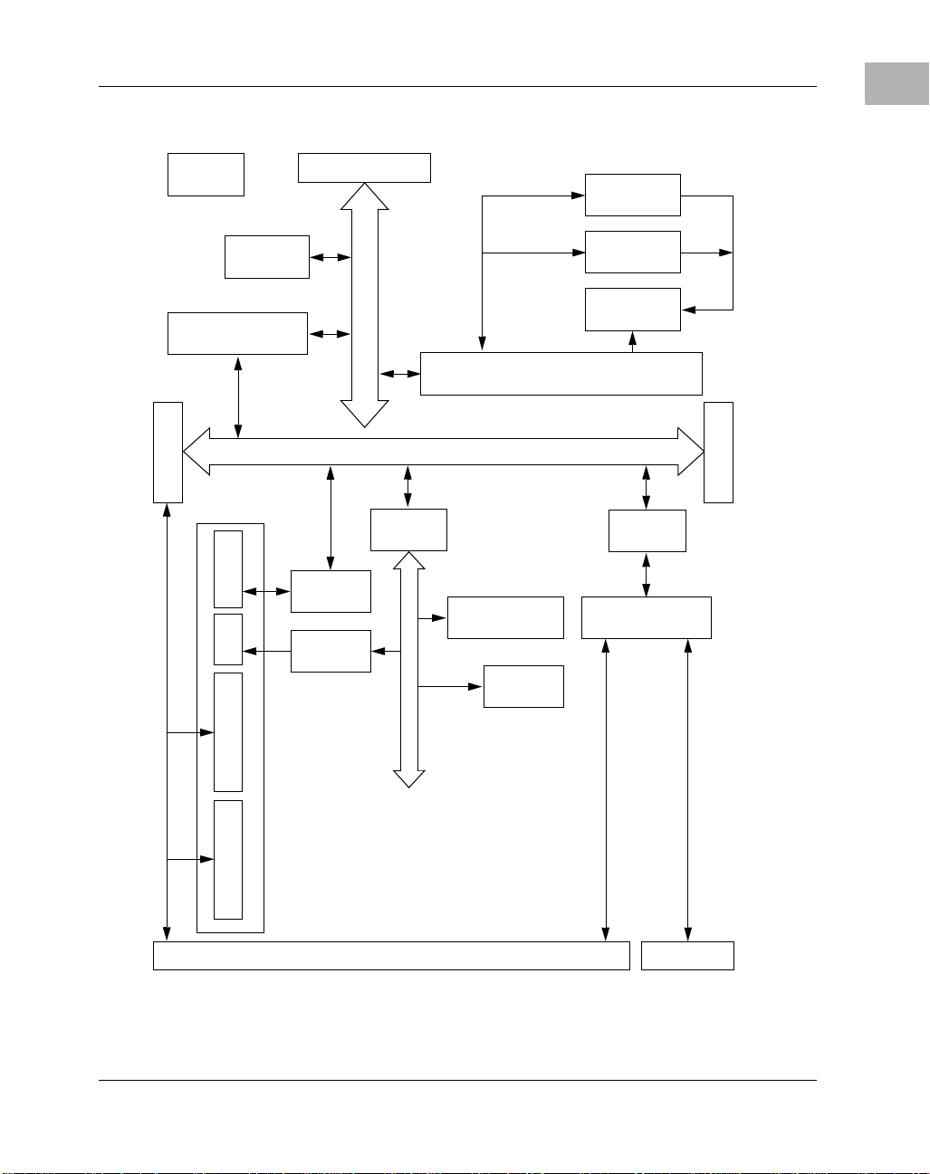
System Block Diagram
1
CLOCK
GENERATOR
PHB & MPIC
RAVEN ASIC
64-BIT PMC SLOT
PROCESSOR
MPC603/604
10BT/100BTX
PORT
SERIAL
DEBUG CONNECTOR
66MHz MPC604 PROCESSOR BUS
33MHz 32/64-BIT PCI LOCAL BUS
W83C553
ETHERNET
DEC21140
PC16550
UART
PIB
ISA BUS
MEMORY CONTROLLER
FALCON CHIP SET
RTC/NVRAM/WD
MK48T59/559
ISA
REGISTERS
DRAM
16/32/64/128MB
Flash
3MB or 5MB
SYSTEM
REGISTERS
VME BRIDGE
UNIVERSE
BUFFERS
PCI EXPANSION
PMC FRONT I/O SLOT
PMC FRONT I/O SLOT
FRONT PA N EL
VME P2 VME P1
2067 9708
Figure 1-1. MVME2300 Series System Block Diagram
http://www.motorola.com/computer/literature 1-5
Page 30

1
Board Description and Memory Maps
Functional Description
The MVME2300 series is a fa mily of single- slot VME processor modules.
It consists of the MPC603/604 processor, the Raven PCI Bridge and
Interrupt Controller, the Falcon ECC Memory Controller chip set, 3MB or
5MB of Flash memory, 16MB to 128MB of ECC-prot ected DRAM, and a
rich set of I/O features.
I/O peripheral devices on the PCI bus are: Ethernet chip, Universe
VMEbus interface ASIC, and two PMC sl ots. Functions provid ed from the
ISA bus are: one asynchronous serial port, a real-time clock,
counters/timers, and a software-readable header.
VMEbus Interface
MVME2300 series boards interface to the VMEbus via the P1 and P2
backplane connectors. MVME2300SC boards use the three-row 96-pin
connectors specified in the original VMEbus standard; non-SCbus
MVME2300 boards use the 5-row 160-pin connectors specified in the
VME64 Extension standard.
Both types of boards draw +5V, +12V, a nd –12V power from the VMEbus
backplane through these two connectors. 3.3V and 2.5V supplies are
regulated onboard from the +5 power.
Front Panel
Front panel connectors on the non-SCbus MVME2300 series boards
include an RJ45 connector for the Ethernet 10BaseT/100BaseTX
interface, and a second RJ45 conne ctor for the async hronous serial debug
port.
Front panel connector s o n the MVME2300SC include an RJ45 connector
for the Ethernet 10BaseT/100BaseTX interface, and a 9-pin DB9
connector for the asynchronous serial debug port.
1-6 Computer Group Literature Center Web Site
Page 31

PCI interface
MVME2300 and MVME2300SC boards are equipped with two IEEE
1386.1 PCI Mezzanine Card (PMC) slots. The PMC slots are 64-bit
capable and support both front and rear I/O.
P2 I/O
Certain pins of each PMC slot connector are routed to VME backplane
connector P2 for use in rear I/O configurations.
On MVME2300 boa rds, pins 1-64 of PMC slot 1 connector J14 are rout ed
to rows C and A of the 5- row DIN P2 connector. Pins 1-46 o f PMC slo t 2
connector J24 are routed to rows D and Z of connector P2.
On MVME2300SC boards, pins 1-32 of PMC slot 1 connector J14 are
routed to rows C and A of th e 3-row DI N P2 connec tor. Pins 1- 32 of PMC
slot 2 connector J2 4 (as wit h J14) ar e routed to rows C a nd A of con nector
P2.
Additional PCI expansion is supported with a 114-pin Mictor connector.
This connection allows s tacking of one or two PMCspan dual-PMC carrier
boards, to increase the I/O capability. Each PMCspan board requires an
additional VME slot.
Programming Model
1
Programming Model
The following sections describe the memory maps for the MVME2300
series boards.
Processor Memory Maps
The Processor memory map is controlled by the Raven ASIC and the
Falcon chip set. The Raven ASIC and the Falcon chip set have flexible
programming Map Decoder registers to customize the system for many
different applications.
http://www.motorola.com/computer/literature 1-7
Page 32

1
Board Description and Memory Maps
Default Processor Memory Map
After a reset, the Raven ASIC and the Falcon chip set provide the default
processor memory map as shown in the following table.
Table 1-2. Default Processor Memory Map
Processor Address
Start End
0000 0000 7FFF FFFF 2G Not mapped
8000 0000 8001 FFFF 128K PCI/ISA I/O Space 1
8002 0000 FEF7 FFFF 2G - 16M -
FEF8 0000 FEF8 FFFF 64K Falcon Registers
FEF9 0000 FEFE FFFF 384K Not mapped
FEFF 0000 FEFF FFFF 64K Raven Registers
FF00 0000 FFEF FFFF 15M Not mapped
FFF0 0000 FFFF FFFF 1M ROM/Flash Bank A or Bank B 2
Size Definition
Not mapped
640K
Notes
1. This default map for PCI/ISA I/O space allows software to
determine whether the system is MPC105-based or Falcon/Ravenbased by examining either the PIB Device ID or the CPU Type
register.
Notes
2. The first Megabyte of ROM/Flash bank A appears at this range af ter
a reset if the rom_b_rv control bit is cleared. If the rom_b_rv control
bit is set, then this address range maps to ROM/Flash bank B.
1-8 Computer Group Literature Center Web Site
Page 33

Processor CHRP Memory Map
The following table shows a recomm ended CHRP memory map from the
point of view of the processor.
Table 1-3. CHRP Memory Map Example
Programming Model
1
Processor Address
Size Definition
Start End
0000 0000 top_dram dram_size System Memory (onboard DRAM) 1, 2
4000 0000 FCFF FFFF 3G - 48M PCI Memory Space:
4000 0000 to FCFF FFFF
FD00 0000 FDFF FFFF 16M Zero-Based PCI/ISA Memory Space
(mapped to 00000000 to 0 0FFFFFF)
FE00 0000 FE7F FFFF 8M Zero-Based PCI/ISA I/O Space
(mapped to 00000000 to 007FFFFF)
FE80 0000 FEF7 FFFF 7.5M Reserved
FEF8 0000 FEF8 FFFF 64K Falcon Regi sters
FEF9 0000 FEFE FFFF 384K Reserved
FEFF 0000 FEFF FFFF 64K Raven Registers 9
FF00 0000 FF7F FFFF 8M ROM/Flash Bank A 1,7
FF80 0000 FF8F FFFF 1M ROM/Flash Bank B 1,7
FF50 0000 FFEF FFFF 6M Reserved
Notes
3,4,8
3,8
3,5,8
FFF0 0000 FFFF FFFF 1M ROM/Flash Bank A or Bank B 7
Notes
1. Programmable via Falcon chip set. For the MVME2300 series,
RAM size is limited to 128MB and ROM/Flash to 4MB.
2. To enable the “Processor- hole” area, program the F alcon chip set to
ignore 0x000A0000 - 0x000BFFFF add ress range and progra m the
Raven to map this address range to PCI memory space.
http://www.motorola.com/computer/literature 1-9
Page 34

1
Board Description and Memory Maps
3. Programmable via Raven ASIC.
4. CHRP requires the star ting addr ess for the PCI memory space to b e
256MB-aligned.
5. Programmable via Raven ASIC for ei ther cont iguous or sprea d-I/O
mode.
6. The actual size of each ROM/Flash bank may vary.
7. The first Megabyte of ROM/Flash bank A appears at this range after
a reset if the rom_b_rv control bit is cleared. If the rom_b_rv control
bit is set then this address range maps to ROM/Flash bank B.
8. This range can be mapped to the VMEbus by programming the
Universe ASIC accordingly. The map shown is the recommended
setting which uses the Sp ecial PCI Sl ave Ima ge and two of the f our
programmable PCI Slave Images.
9. The only method of generating a PCI Inter rupt Acknowledge cycle
(8259 IACK) is to perform a read access to the Raven’s PIACK
register at 0xFEFF0030.
The following table shows the programmed values for the associated
Raven MPC registers for the processor CHRP memory map.
Table 1-4. Raven MPC Register Val ues for CHRP Memory Map
Address Register Name Register Value
FEFF 0040 MSADD0 4000 FCFF
FEFF 0044 MSOFF0 & MSATT0 0000 00C2
FEFF 0048 MSADD1 FD00 FDFF
FEFF 004C MSOFF1 & MSATT1 0300 00C2
FEFF 0050 MSADD2 0000 0000
FEFF 0054 MSOFF2 & MSATT2 0000 0002
FEFF 0058 MSADD3 FE00 FE7F
FEFF 005C MSOFF3 & MSATT3 0200 00C0
1-10 Computer Group Literature Center Web Site
Page 35

Programming Model
Processor PREP Memory Map
The Raven/Falcon chip set can be programmed for PREP-compatible
memory map. The following table shows the PREP memory map of the
MVME2300 series from the point of view of the processor.
Table 1-5. PREP Memory Map Example
Processor Address
Size Definition Notes
Start End
0000 0000 top_dram dram_size System Memory (onboard DRAM) 1
1
8000 0000 BFFF FFFF 1G Zero-Based PCI I/O Space:
0000 0000 - 3FFFF FFFF
C000 0000 FCFF FFFF 1G - 48M Zero-Based PCI/ISA Memory Space:
0000 0000 - 3CFFFFFF
FD00 0000 FEF7 FFFF 40.5M Reserved
FEF8 0000 FEF8 FFFF 64K Falcon Registers
FEF9 0000 FEFE FFFF 384K Reserved
FEFF 0000 FEFF FFFF 64K Raven Registers 6
FF00 0000 FF7F FFFF 8M ROM/Flash Bank A 1, 3
FF80 0000 FF8F FFFF 1M ROM/Flash Bank B 1, 3
FF90 0000 FFEF FFFF 6M Reserved
FFF0 0000 FFFF FFFF 1M ROM/Flash Bank A or Bank B 4
2
2, 5
Notes
1. Programmable via Falcon chip set. For the MVME2300 series,
RAM size is limited to 128MB and ROM/Flash to 4MB.
2. Programmable via Raven ASIC.
3. The actual size of each ROM/Flash bank may vary.
http://www.motorola.com/computer/literature 1-11
Page 36

1
Board Description and Memory Maps
4. The first Megabyte of ROM/Flash bank A appears at this range af ter
a reset if the rom_b_rv control bit is cleared. If the rom_b_rv control
bit is set then this address range maps to ROM/Flash bank B.
5. This range can be mapped to the VMEbus by programming the
Universe ASIC accordingly.
6. The only method of generating a PCI Inter rupt Acknowledge cycle
(8259 IACK) is to perform a read access to the Raven’s PIACK
register at 0xFEFF0030.
The following table shows the programmed values for the associated
Raven MPC registers for the processor PREP memory map.
Table 1-6. Raven MPC Register Values for PREP Memory Map
Address Register Name Register Value
FEFF 0040 MSADD0 C000 FCFF
FEFF 0044 MSOFF0 & MSATT0 4000 00C2
FEFF 0048 MSADD1 0000 0000
FEFF 004C MSOFF1 & MSATT1 0000 0002
FEFF 0050 MSADD2 0000 0000
FEFF 0054 MSOFF2 & MSATT2 0000 0002
FEFF 0058 MSADD3 8000 BFFF
FEFF 005C MSOFF3 & MSATT3 8000 00C0
PCI Configuration Access
PCI Configuration acc esses ar e accomplis hed via t he CONFIG_ADD and
CONFIG_DAT registers. These two registers are implemented in the
Raven ASIC. In the CHRP memory map example, the CONFIG_ADD and
CONFIG_DAT registers are located at 0xFE000CF8 and 0xFE000CFC,
respectively. With the PREP memory map, the CONFIG_ADD register
and the CONFIG_DAT register are located at 0x80000CF8 and
0x80000CFC, respectively.
1-12 Computer Group Literature Center Web Site
Page 37

PCI Memory Maps
The PCI memory map is controlled by the Raven ASIC and the Universe
ASIC. The Raven ASIC and the Universe ASIC have flexible
programming Map Decoder registers to customize the system to fit many
different applications.
Default PCI Memory Map
After a reset, the Raven ASIC and the Univer se ASIC turn all the PCI slave
map decoders off. Software must program the appropriate map decoders
for a specific environment.
PCI CHRP Memory Map
The following table shows a PCI memory map of the MVME2300 series
that is CHRP-compatible from the point of view of the PCI local bus.
Table 1-7. PCI CHRP Memory Map
Programming Model
1
PCI Address
Start End
0000 0000 top_dram dram_size Onboard ECC DRAM 1
4000 0000 EFFF FFFF 3G - 256M VMEbus A32/D32 (Super/Program) 3
F000 0000 F7FF FFFF 128M VMEbus A32/D16 (Super/Program) 3
F800 0000 F8FE FFFF 16M - 64K VMEbus A24/D16 (Super/Program) 4
F8FF 0000 F8FF FFFF 64K VMEbus A16/D16 (Super/Program) 4
F900 0000 F9FE FFFF 16M - 64K VMEbus A24/D32 (Super/Data) 4
F9FF 0000 F9FF FFFF 64K VMEbus A16/D32 (Super/Data) 4
FA00 0000 FAFE FFFF 16M - 64K VMEbus A24/D16 (User/Program) 4
FAFF 0000 FAFF FFFF 64K VMEbus A16/D16 (User/Program) 4
FB00 0000 FBFE FFFF 16M - 64K VMEbus A24/D32 (User/Data) 4
FBFF 0000 FBFF FFFF 64K VMEbus A16/D32 (User/Data) 4
http://www.motorola.com/computer/literature 1-13
Size Definition Notes
Page 38

1
Board Description and Memory Maps
Table 1-7. PCI CHRP Memory Map (Continued)
PCI Address
Size Definition Notes
Start End
FC00 0000 FC03 FFFF 256K RavenMPIC 1
FC04 0000 FCFF FFFF 16M - 256K PCI Memory Space
FD00 0000 FDFF FFFF 16M PCI Memory Space
or System Memory Alias Space
(mapped to 00000000 to 00FFFFFF)
FE00 0000 FFFF FFFF 48M Reserved
Notes
1. Programmable via the Rav en’s PCI Config uration reg isters. For th e
MVME2300 series, RAM size is limited to 128MB.
2. To enable the CHRP “io-hole”, program the Raven to ignore the
0x000A0000 - 0x000FFFFF address range.
3. Programmable mapping via the four PCI Slave Images in the
Universe ASIC.
4. Programmable mapping via the Special Slave Image (SLSI) in the
Universe ASIC.
1
1-14 Computer Group Literature Center Web Site
Page 39

Programming Model
The following table shows the programmed values for the associated
Raven PCI registers for the PCI CHRP memory map.
Table 1-8. Raven PCI Register Values for CHRP Memory Map
1
Configuration
Address Offset
$14 RavenMPIC MBASE FC00 0000 FC00 0000
$80 PSADD0 0000 3FFF 0100 3FFF
$84 PSOFF0 & PSATT0 0000 00FX 0000 00FX
$88 PSADD1 0000 0000 FD00 FDFF
$8C PSOFF1 & PSATT1 0000 0000 0000 00FX
$90 PSADD2 0000 0000 0000 0000
$94 PSOFF2 & PSATT2 0000 0000 0000 0000
$98 PSADD3 0000 0000 0000 0000
$9C PSOFF3 & PSATT3 0000 0000 0000 0000
Configuration
Register Name
Register Value
(Aliasing OFF)
Register Value
(Aliasing ON)
The next table shows the programmed values for the associated Universe
PCI registers for the PCI CHRP memory map.
Table 1-9. Universe PCI Register Values for CHRP Memory Map
Configuration
Address Offset
Configuration
Register Name
Register Value
$100 LSI0_CTL C082 5100
$104 LSI0_BS 4000 0000
$108 LSI0_BD F000 0000
$10C LSI0_TO XXXX 0000
$114 LSI1_CTL C042 5100
$118 LSI1_BS F000 0000
$11C LSI1_BD F800 0000
http://www.motorola.com/computer/literature 1-15
Page 40

1
Board Description and Memory Maps
Table 1-9. Universe PCI Register Values for CHRP Memory Map (Continued)
Configuration
Address Offset
$120 LSI1_TO XXXX 0000
$128 LSI2_CTL 0000 0000
$12C LSI2_BS XXXX XXXX
$130 LSI2_BD XXXX XXXX
$134 LSI2_TO XXXX XXXX
$13C LSI3_CTL 0000 0000
$140 LSI3_BS XXXX XXXX
$144 LSI3_BD XXXX XXXX
$148 LSI3_TO XXXX XXXX
$188 SLSI C0A053F8
PCI PREP Memory Map
The following table shows a PCI memory map of the MVME2300 series
boards that is PREP-compatible from the point of view of the PCI local
bus.
Configuration
Register Name
Register Value
Table 1-10. PCI PREP Memory Map
PCI Address
Start End
0000 0000 00FF FFFF 16M PCI/ISA Memory Space
0100 0000 2FFF FFFF 752M VMEbus A32/D32 (Super/Program) 3
3000 0000 37FF FFFF 128M VMEbus A32/D16 (Super/Program) 3
3800 0000 38FE FFFF 16M - 64K VMEbus A24/D16 (Super/Program) 4
1-16 Computer Group Literature Center Web Site
Size Definition Notes
Page 41

Programming Model
Table 1-10. PCI PREP Memory Map (Continued)
1
PCI Address
Start End
38FF 0000 38FF FFFF 64K VMEbus A16/D16 (Super/Program) 4
3900 0000 39FE FFFF 16M - 64K VMEbus A24/D32 (Super/Data) 4
39FF 0000 39FF FFFF 64K VMEbus A16/D32 (Super/Data) 4
3A00 0000 3AFE FFFF 16M - 64K VMEbus A24/D16 (User/Program) 4
3AFF 0000 3AFF FFFF 64K VMEbus A16/D26 (User/Program) 4
3B00 0000 3BFE FFFF 16M - 64K VMEbus A24/D32 (User/Data) 4
3BFF 0000 3BFF FFFF 64K VMEbus A16/D32 (User/Data) 4
3C00 0000 7FFF FFFF 1G + 64M PCI Memory Space
8000 0000 FBFF FFFF 2G - 64M Onboard ECC DRAM 1
FC00 0000 FC03 FFFF 256K RavenMPIC 1
FC04 0000 FF FF FFFF 64M - 256K PCI Memory Space
Size Definition Notes
Notes
1. Programmable via the Rav en’s PCI Config uration reg isters. For th e
MVME2300 series, RAM size is limited to 128MB.
2. To enabled the CHRP “io-hole”, program the Raven to ignore the
0x000A0000 - 0x000FFFFF address range.
3. Programmable mapping via the four PCI Slave Images in the
Universe ASIC.
4. Programmable mapping via the Special Slave Image (SLSI) in the
Universe ASIC.
http://www.motorola.com/computer/literature 1-17
Page 42

1
Board Description and Memory Maps
The following table shows the programmed values for the associated
Raven PCI registers for the PREP-compatible memory map.
Table 1-11. Raven PCI Register Values for PREP Memory Map
Configuration
Address Offset
$14 RavenMPIC MBASE FC00 0000
$80 PSADD0 8000 FBFF
$84 PSOFF0 & PSATT0 8000 00FX
$88 PSADD1 0000 0000
$8C PSOFF1 & PSATT1 0000 0000
$90 PSADD2 0000 0000
$94 PSOFF2 & PSATT2 0000 0000
$98 PSADD3 0000 0000
$9C PSOFF3 & PSATT3 0000 0000
Configuration
Register Name
Register Value
1-18 Computer Group Literature Center Web Site
Page 43

Programming Model
The next table shows the programmed values for the associated Universe
PCI registers for the PCI PREP memory map.
Table 1-12. Universe PCI Register Values for PREP Memory Map
1
Configuration
Address Offset
$100 LSI0_CTL C082 5100
$104 LSI0_BS 0100 0000
$108 LSI0_BD 3000 0000
$10C LSI0_TO XXXX 0000
$114 LSI1_CTL C042 5100
$118 LSI1_BS 3000 0000
$11C LSI1_BD 3800 0000
$120 LSI1_TO XXXX 0000
$128 LSI2_CTL 0000 0000
$12C LSI2_BS XXXX XXXX
$130 LSI2_BD XXXX XXXX
$134 LSI2_TO XXXX XXXX
$13C LSI3_CTL 0000 0000
Configuration
Register Name
Register Value
$140 LSI3_BS XXXX XXXX
$144 LSI3_BD XXXX XXXX
$148 LSI3_TO XXXX XXXX
$188 SLSI C0A05338
http://www.motorola.com/computer/literature 1-19
Page 44

1
Board Description and Memory Maps
VMEbus Mapping
The processor can access any address range in the VMEbus with the help
of the Universe ASIC’s address translation capabilities. The Processor
Memory Map section shows the recommended mapping.
VMEbus Master Map
The figure below illustrates how VMEbus master mapping is
accomplished. (Note that for MVME2300 series boards, RAM size is
limited to 128MB.)
VMEBUS
PROGRAMMABLE
SPACE
ONBOARD
MEMORY
PCI MEMORYPROCESSOR
NOTE 2
PCI MEMORY
SPACE
PCI/ISA
MEMORY SPACE
PCI
I/O SPACE
MPC
RESOURCES
NOTE 1
NOTE 1
NOTE 3
VME A24
VME A16
VME A24
VME A16
VME A24
VME A16
VME A24
VME A16
11553.00 9609
Figure 1-2. VMEbus Master Mapping
1-20 Computer Group Literature Center Web Site
Page 45

Notes
1. Programmable mapping done by the Raven ASIC.
2. Programmable mapping via the four PCI Slave Images in the
3. Programmable mapping via the Special Slave Image (SLSI) in the
VMEbus Slave Map
The four programmable VME Slave images in the Universe ASIC give
other VMEbus masters access to any devices on the board. The
combination of the four Universe VME Slave images and the four Raven
PCI Slave decoders offers great flexibility in mapping the system
resources as seen from the VMEbus.
In most applications, the VMEbus needs to see only the system memory
and, perhaps, the software interrupt registers (SIR1 and SIR2 registers).
For an example of the VMEbus slave map, refer to the figure below:
Programming Model
1
Universe ASIC.
Universe ASIC.
http://www.motorola.com/computer/literature 1-21
Page 46

1
Board Description and Memory Maps
Processor
Onboard
Memory
ISA Space
Software INT
Registers
PCI Memory
NOTE 2
NOTE 1
NOTE 1
PCI I/O Space
NOTE3
Figure 1-3. VMEbus Slave Mapping
VMEbus
1896 9609
Notes
1. Programmable mapping via the four VME Slave Images in the
Universe ASIC.
2. Programmable mapping via PCI Slave Images in the Raven ASIC.
3. Fixed mapping via the PIB device.
1-22 Computer Group Literature Center Web Site
Page 47

Programming Model
The following table shows the programmed values for the associated
Universe registers for the VMEbus slave function.
Table 1-13. Universe PCI Register Values for VMEbus Slave Map Example
1
Configuration
Address Offset
$F00 VSI0_CTL C0F2 0001 C0F2 0001
$F04 VSI0_BS 4000 0000 4000 0000
$F08 VSI0_BD 4000 1000 4000 1000
$F0C VSI0_TO C000 1000 C000 1000
$F14 VSI1_CTL E0F2 00C0 E0F2 00C0
$F18 VSI1_BS 1000 0000 1000 0000
$F1C VSI1_BD 2000 0000 2000 0000
$F20 VSI1_TO F000 0000 7000 0000
$F28 VSI2_CTL 0000 0000 0000 0000
$F2C VSI2_BS XXXX XXXX XXXX XXXX
$F30 VSI2_BD XXXX XXXX XXXX XXXX
$F34 VSI2_TO XXXX XXXX XXXX XXXX
$F3C VSI3_CTL 0000 0000 0000 0000
Configuration
Register Name
Register Value
(CHRP)
Register Value
(PREP)
$F40 VSI3_BS XXXX XXXX XXXX XXXX
$F44 VSI3_BD XXXX XXXX XXXX XXXX
$F48 VSI3_TO XXXX XXXX XXXX XXXX
http://www.motorola.com/computer/literature 1-23
Page 48

1
Board Description and Memory Maps
The register values in the table yield the following VMEbus slave map:
Table 1-14. VMEbus Slave Map Example
VMEbus Address
Size CHRP Map PREP Map
Range Mode
4000 0000 4000 0FFF
1000 0000 1FFF FFFF
A32 U/S/P/D
D08/16/32
A32 U/S/P/D
D08/16/32/64
RMW
4K
256M
PCI/ISA I/O Space:
0000 1000 - 0000 1FFF
PCI/ISA Memory Space
(On-board DRAM)
0000 0000 - 0FFF FFFF
Falcon-Controlled System Registers
The Falcon chip set latches the states of the DRAM data lines onto the
PR_STAT1 and PR_STAT2 registers. MVME2300 seri es boards use these
status registers to provide the system configuration information. In
addition, the Falcon chip set performs the decode and control for an
external register port. This function is utilized by MVME2300 series
boards to provide the system control registers.
Table 1-15. System Register Summary
BIT # ---->
FEF80400
FEF80404
FEF88000
FEF88300
0123456789101112131415161718192021222324252627282930
System Configuration Register (Upper Falcon’s PR_STAT1)
Memory Configuration Register (Lower Falcon’s PR_STAT1)
System External Cache
Control Register
CPU Control Register
PCI/ISA I/O Space:
0000 1000 - 0000 1FFF
PCI/ISA Memory Space
(On-board DRAM)
8000 0000 - 8FFF FFFF
31
The following subsections describe these system registers in detail.
1-24 Computer Group Literature Center Web Site
Page 49

Programming Model
System Configuration Register (SYSCR)
The states of the RD[0:31] DRAM data pins, which have weak internal
pull-ups, are l atched by the upper Falcon chip at a ris ing edge of th e powerup reset and stored in this System Configuration register to provide some
information about t he system. Configuration is accomplished wit h external
pull-down resistors. This 32-bit read-only register is defined as follows:
REG System Configuration Register - $FEF80400
BIT
FIELD
OPER Read Only
RESET $FD 1111 1111 0111 1111 1 1 $F
012345678
SYSID
101112131415161718192021222324252627282930
9
SYSCLK
SYSXC P0STAT P1STAT
SYSID System Identification. This field specifies the type of the
overall system configuration so that the software may
appropriately hand le any softwa re visible differences . For
the MVME2300 series, this field returns a value of $FD.
SYSCLK System Clock Speed. This field rela ys the system clock
speed and the PCI clock speed information as follows:
1
31
SYSCLK Value System Cloc k Speed PCI Clock Speed
0B0000 to 0B1100 Reserved Reserved
0B1101
0B1110
0B1111
http://www.motorola.com/computer/literature 1-25
50MHz 25MHz
60MHz 30MHz
66.66MHz 33.33MHz
Page 50

1
Board Description and Memory Maps
SYSXC System External Cache Size. The MVME2300 series does
not offer any external caching options. Reads from this
field will always return a hardwired value of 0b1111
indicating the absence of external caching.
P0/1STAT Processor 0/1 Status. This field is encoded as follows:
P0/1STAT Value Processor 0/1 Present
0B0000 to 0B0011 Reserved Reserved
0B0100 Yes 1M
0B0101 Yes 512K
0B0110 Yes 256K
0B0111 Yes None
0B1000 to 0B1111 No N/A
External In-line Cache
Size
1-26 Computer Group Literature Center Web Site
Page 51

Memory Configuration Register (MEMCR)
The states of the RD[00:31] DRAM data pins, which have weak internal
pull-ups, are lat ched by the lowe r Falcon chip a t a rising edge of the powerup reset and stored in t his Memory Configura tion register t o provide some
information about the system memory. Configuration is accomplished
with external pull-d own resistors. Thi s 32-bit read-on ly register is defined
as follows :
REG Memory Configuration Register - $FEF80404
BIT
32333435363738394041424344454647484950515253545556575859606162
M_SIZE0
M_FREF
M_SIZE1
M_SPD0
M_SPD1
R_A_TYP0
R_A_TYP1
R_A_TYP2
R_B_TYP0
R_B_TYP1
R_B_TYP2
L2_TYPE0
L2_TYPE1
L3_TYPE3
L2_TYP2
L2_PLL0
L2_PLL1
L2_PLL2
FIELD
OPER
X
RESET
X1X
X
1
X1XXX1XXXXXXXXXXX
1
M_SIZE[0:1]
Memory Size. This field is encoded as follows:
Programming Model
FLSHP0_
1
FLSHP1_
XXX
FLSHP2-
L2_PLL3
1
1
63
111
M_SIZE[0:1] Total Memory On Boar d
0B00 16 Megabytes
0B01
0B10
0B11
32 Megabytes
64 Megabytes
128 Megabytes
M_FREF Block A/B/C/D Fast Refresh. When this bit is set, it
indicates that a DRAM block requires faster refresh rate.
If any of the four blocks requires faster refresh rate then
the ram ref
http://www.motorola.com/computer/literature 1-27
control bit should be set.
Page 52

1
Board Description and Memory Maps
M_SPD[0:1]
Memory Speed. This field relays the memory speed
information as follows:
M_SPD[0:1] DRAM Speed DRAM Type
0B00 70ns Past Page
0B01
0B10
0B11
These two bi ts reflect the combined status of the four
blocks of DRAM. Initialization software uses this
information to program the ram_spd0
control bits in the Falcon’s Chip Revision register.
R_A/B_TYP[0:2]
ROM/Flash Type. This field is encoded as follows:
ROM_A/B_TYP[0:2] ROM/Flash Type
0B000 to 0B101 Reserved
0B110
0B111
Intel 16-bit wide Flash with 16K Bottom Boot
Block
Unknown type (i.e. ROM/Flash sockets)
60ns Fast Page
Reserved Reserved
50ns EDO
and ram_spd1
Note The device width differs from the width of the Flash bank. If the
bank width is 64 bits and the device width is 16 bits, then the
Flash bank consists of four Flash devices.
L2_TYPE[0:3]
L2 Memory Type. This field is encoded as follows:
L2_TYPE[0:3] Configuration
0B0000 Late write Sync
0B0001
0B0010 to 0B1111
1-28 Computer Group Literature Center Web Site
Pipelined Sync Burst
Reserved
Page 53

L2_PLL[0:3]
L2 Core Frequency to L2 Frequ ency di vider. This field is
encoded as follows:
FLSHP[0:2]
Bank A Flash memory size. This field is encoded as
follows:
Flash Size FLSHP0_ FLSHP1_ FLS H P2_
1MB000
2MB
4MB
8MB
16MB
32MB
64MB
No Flash
Programming Model
PLL Value] Size
0B0000 Disable
0B0001
0B0010
0B0011
0B0100
0B0101
0B0110 to 0B1111
0 0 1
0 1 0
0 1 1
1 0 0
1 0 1
1 1 0
1 1 1
1.5
2.5
Reserved
1
1
2
3
System External Cache Control Register (SXCCR)
The MVME2300 and MVME2300SC boards do not implement this
register. Writes to t his r egister locat ion ($FE F88000) wi ll hav e no syst em
effects. Reads from this register location will return undefined data.
http://www.motorola.com/computer/literature 1-29
Page 54

1
Board Description and Memory Maps
Processor 0 External Cache Control Register (P0XCCR)
The MVME2300 and MVME2300SC boards do not implement this
register. Writes to t his r egister locat ion ($FE F88100) wi ll hav e no syst em
effects. Reads from this register location will return undefined data.
Processor 1 External Cache Control Register (P1XCCR)
The MVME2300 and MVME2300SC boards do not implement this
register. Writes to t his r egister locat ion ($FE F88200) wi ll hav e no syst em
effects. Reads from this register location will return undefined data.
CPU Control Register
The CPU Control register is accessed via the RD[32:39] data lines of the
upper Falcon device. This 8-bit register is defined as follows:
REG CPU Control Register - $FEF88300
BIT 01234567
FIELD
LEMODE
P0_TBEN
OPER RRRR/WRRRR
RESET 1001XXXX
LEMODE Little Endian Mode. This bit must be set in conjunction
with the LEND bit in the Raven for little-end ian mode.
P0_TBEN Processor 0 Time Base Enable. When this bit is cleared,
the TBEN pi n of the processor will be driven low.
1-30 Computer Group Literature Center Web Site
Page 55

ISA Local Resource Bus
W83C553 PIB Registers
The PIB contains ISA Bridge I/O registers for various functions. These
registers are actually accessible from the PCI bus. Refer to the W83C553
Data Book for details.
16550 UART
The 16550 UART provides the MVME2300 series boards with an
asynchronous serial port. Refer to the 16550 Data Sheet for additional
details and programming information.
The following table shows the mapping of the 16550 registers within the
MVME2300 series boards’ ISA I/O space beginning at address 0x3F8:
Table 1-16. 16550 Access Registers
ISA Local Resource Bus
1
ISA I/O Address Function
0000 03F8
0000 03F9 Interrupt Enable
0000 03FA
0000 03FB Line Control
0000 03FC MODEM control
0000 03FD Line Status
0000 03FE MODEM Status
0000 03FF Scratch
http://www.motorola.com/computer/literature 1-31
Receiver Buffer (Read);
Transmitter Holding (Write)
Interrupt Identification (Read);
FIFO Control (Write)
Page 56

1
Board Description and Memory Maps
General-Purpose Readable Jumpers
Headers J10 (on the MVME2300SC) and J17 (on the MVME2300)
provide eight software-readable jumpers. These jumpers can be read as a
register at ISA I/O address $801 (hexadecimal). Bit 0 is associated with
header pins 1-2; bit 7 is associ ated with pi ns 15-16. The bit values are r ead
0 when a jumper is installed, and as a 1 when the jumper is removed.
as a
The PowerPC firmware, PPCBug, reserves all bits, SRH0 to SRH7. The
board is shipped from the factory with J10 / J17 set to all
all pins), a s shown in Figure 1-4.
0s (jumpers on
PPCBug INSTALLED
Reserved for future use
Reserved for future use
Reserved for future use
Reserved for future use
Reserved for future use
Reserved for future use
Reserved for future use
16Bit 7 (SRH7)
Reserved for future use
Bit 0 (SRH0)
Bit 1 (SRH1)
Bit 2 (SRH2)
Bit 3 (SRH3)
Bit 4 (SRH4)
Bit 5 (SRH5)
Bit 6 (SRH6)
J10/J17
12
15
Figure 1-4. General-Purpose Software-Readable Header
NVRAM/RTC and Watchdog Timer Registers
The M48T59/559 provides th e MVME2300 s erie s board s with 8K of non volatile SRAM, a time-of-day clock, and a watchdog timer. Accesses to
the M48T59/559 are accomplished via three registers:
❏ The NVRAM/RTC Address Strobe 0 register
❏ The NVRAM/RTC Address Strobe 1 register
❏ The NVRAM/RTC Data Port register
1-32 Computer Group Literature Center Web Site
Page 57

ISA Local Resource Bus
The NVRAM/RTC Address Strobe 0 register la tches the lower 8 bits of the
address and the NVRAM/R TC Address St robe 1 regist er latches the upper
5 bits of the address.
Table 1-17. M48T59/559 Access Registers
PCI I/O Address Function
0000 0074 NVRAM/RTC Address Strobe 0 (A7 - A0)
0000 0075 NVRAM/RTC Address Strobe 1 (A15 - A8)
0000 0077 NVRAM/RTC Data Register
The NVRAM and RTC are accessed through the above three registers.
When accessing an NVRAM/RTC location, follow this procedure:
1. Write the low address (A7-A0) of the NVRAM to the
NVRAM/RTC STB0 register,
2. Write the high address (A15-A8) of the NVRAM to the
NVRAM/RTC STB1 register, and
3. Then read or write the NVRAM/RTC Data Port.
1
Refer to the M48T59 Data Sheet for additional details and programming
information.
Module Configuration and Status Registers
Four registers provide the configuration and status information about the
board. These registers are listed in the following table:
Table 1-18. Module Configuration and Status Registers
PCI I/O Address Function
0000 0800 CPU Configuration Register
0000 0802 Base Module Feature Register
0000 0803 Base Module Status Register
0000 08C0 - 0000 08C1 Seven-Segment Display Register
http://www.motorola.com/computer/literature 1-33
Page 58

1
Board Description and Memory Maps
The following subsections describe the configuration and status registers
in detail.
CPU Configuration Register
The CPU Configuration register is an 8-bit register located at ISA I/O
address x0800. This register is defined for the MVME2300 series to
provide some backward compatibility with older MVME1600 products.
The Base Module Status register should be used to identify the base
module type and the System Configuration register should be used to
obtain information about the overall system.
REG Old CPU Configuration Register - $FE000800
BIT SD7 SD6 SD5 SD4 SD3 SD2 SD1 SD0
FIELD CPUTYPE
OPER RR
RESET $E $F
CPUTYPE
CPU Type. This field will always read as $E for the
MVME2300 series. (The whole register will read $EF.)
The System Configuration register should be used for
additional information.
1-34 Computer Group Literature Center Web Site
Page 59

ISA Local Resource Bus
Base Module Feature Register
The Base Module Feature register is an 8-bit register providing the
configuration information about the MVME2300-series VME processor
module. This read-only register is located at ISA I/O address x0802.
REG Base Module Feature Register - Offset $0802
BIT SD7 SD6 SD5 SD4 SD3 SD2 SD1 SD0
FIELD
OPER RRRRRRRR
RESET X1XXX1X1
PCIXP_
PMC2P_
PMC1P_
VMEP_
LANP_
PCIXP_ PCI Expansion Slot present. If set, there is no PCIX
device installed. If cleared, the PCIX slot contains a PCI
Mezzanine Card.
1
PMC2P_ PMC Slot 2 present. If set, there is no PCI Mezzanine
Card installed in PMC Slot 2. If cleared, PMC Slot 2
contains a PMC.
PMC1P_ PMC Slot 1 present. If set, there is no PCI Mezzanine
Card installed in PMC Slot 1. If cleared, PMC Slot 1
contains a PMC.
VMEP_ VMEbus present. If set, there is no VMEbus interface. If
cleared, VMEbus interface is supported.
LANP_ Ethernet present. If set, there is no Ethernet transceiver
interface. If cleared, there is on-boa rd Ethernet support.
http://www.motorola.com/computer/literature 1-35
Page 60

1
Board Description and Memory Maps
Base Module Status Register (BMSR)
The Base Module Status register is an 8-bit read-only register located at
ISA I/O address x0803.
REG Base Module Status Register - Offset $0803
BIT SD7 SD6 SD5 SD4 SD3 SD2 SD1 SD0
FIELD BASE_TYPE
OPER R
RESET 1111 N/A
BASE_TYPE
Base Module Type. This four-bit field is used to provide
the category of the bas e module and i s defined as follows:
BASE_TYPE Value Base Module Type
$0 to $8 Reserved
$9 MVME2300
$A to $F Reserved
1-36 Computer Group Literature Center Web Site
Page 61

ISA Local Resource Bus
Seven-Segment Display Register
Note T his register is NOT USED on the MVME2300-series
boards.
This 16-bi t register allows data to be sent to the 4-d igit hexadec imal
diagnostic display. The register also allows the data to be read back.
REG 7-Segment Display Register - Offset $08C0
SD15
SD14
SD13
SD12
SD11
SD10
SD9
SD8
SD7
SD6
SD5
SD4
SD3
SD2
SD1
SD0
BIT
FIELD DIG3[3:0] DIG2[3:0] DIG1[3:0] DIG0[3:0]
OPER R/W
RESET XXXXXXXXXXXXXXXX
DIG3[3:0] Hexadecimal value of the most significant digit.
DIG2[3:0] Hexadecimal value of the third significant digit.
1
DIG1[3:0] Hexadecimal value of the second significant digit.
DIG0[3:0] Hexadecimal value of the least significant digit.
VME Registers
The registers listed in the table below provide the following functions for
the VMEbus interface:
❏ A software interrupt capability
❏ A location monitor function
❏ A geographical address status
For these registers to be a ccessi ble f rom the VM Ebus, th e Univer se ASIC
must be programmed t o map VMEbus Slave Image 0 i nto t he appropriate
PCI I/O address range. R efer to the VMEbus Slave Map section for
additional details.
http://www.motorola.com/computer/literature 1-37
Page 62

1
Board Description and Memory Maps
Table 1-19. VME Registers
PCI I/O Address Function
0000 1000 SIG/LM Control Register
0000 1001 SIG/LM Status Register
0000 1002 VMEbus Location Monitor Upper Base Address
0000 1003 VMEbus Location Monitor Lower Base Address
0000 1004 VMEbus Semaphore Register 1
0000 1005 VMEbus Semaphore Register 2
0000 1006 VMEbus Geographical Address Status
These registers are described in the following subsections.
LM/SIG Control Register
The LM/SIG Control register is an 8-bit register located at ISA I/O address
x1000. This register provides a method to generate software interrupts.
The Universe ASIC is programmed so that this register can be accessed
from the VMEbus to generate software interrupts to the processor(s).
REG LM/SIG Control Register - Offset $1000
BIT SD7 SD6 SD5 SD4 SD3 SD2 SD1 SD0
FIELD
OPER WRITE-ONLY
RESET 00000000
SET
SIG1
SET
SIG0
SET
LM1
SET
LM0
CLR
SIG1
CLR
SIG0
CLR
LM1
CLR
LM0
SET_SIG1
Writing a 1 to this bit will set the SIG1 status bit.
SET_SIG0
Writing a 1 to this bit will set the SIG0 status bit.
1-38 Computer Group Literature Center Web Site
Page 63

SET_LM1
SET_LM0
CLR_SIG1
CLR_SIG0
CLR_LM1
CLR_LM0
LM/SIG Status Register
The LM/SIG Status regi st er is an 8-bit regist er l ocated at ISA I/O a ddre ss
x1001. This register, in conjunction with the LM/SIG Control register,
provides a method to generate interrupts. The Universe ASIC is
programmed so that this register can be accessed from the VMEbus to
provide a capability to generate software interrupts to the onboard
processor(s) from the VMEbus.
ISA Local Resource Bus
1
Writing a 1 to this bit will set the LM1 status bit.
Writing a 1 to this bit will set the LM0 status bit.
Writing a 1 to this bit will clear the SIG1 status bit.
Writing a 1 to this bit will clear the SIG0 status bit.
Writing a 1 to this bit will clear the LM1 status bit.
Writing a 1 to this bit will clear the LM0 status bit.
REG LM/SIG Status Register - Offset $1001
BIT SD7 SD6 SD5 SD4 SD3 SD2 SD1 SD0
FIELD EN
SIG1
OPER R/W READ-ONLY
RESET 00000000
EN
SIG0
EN
LM1
EN
LM0
SIG1 SIG0 LM1 LM0
EN_SIG1 When the EN_SIG1 bit is set, a n LM/SIG Interrupt 1 is
generated if the SIG1 bit is asserted.
EN_SIG0 When the EN_SIG0 bit is set, a n LM/SIG Interrupt 0 is
generated if the SIG0 bit is asserted.
http://www.motorola.com/computer/literature 1-39
Page 64

1
Board Description and Memory Maps
EN_LM1 When the EN _LM1 bit is set, an LM/SIG Interrupt 1 is
generated and the LM1 bit is asserted.
EN_LM0 When the EN _LM0 bit is set, an LM/SIG Interrupt 0 is
generated and the LM0 bit is asserted.
SIG1 SIG1 status bit . This bit can only be se t by the SET_LM1
control bit. It can onl y be cle ar ed by a reset or by writing
a 1 to the CLR_LM1 control bit.
SIG0 SIG0 status bit . This bit can only be se t by the SET_LM0
control bit. It can onl y be cle ar ed by a reset or by writing
a 1 to the CLR_LM0 control bit.
LM1 LM1 status bit. This bit can be set by either the location
monitor function or the SET_LM1 control bit. LM1
correspond to offset 3 from the location monitor base
address. This bit can only be cleared by a reset or by
writing a 1 to the CLR_LM1 control bit.
LM0 LM0 status bit. This bit can be set by either the location
monitor function or the SET_LM0 control bit. LM0
correspond to offset 1 from the location monitor base
address. This bit can only be cleared by a reset or by
writing a 1 to the CLR_LM0 control bit.
1-40 Computer Group Literature Center Web Site
Page 65

ISA Local Resource Bus
Location Monitor Upper Base Address Register
The Location Monitor Upper Base Address register is an 8-bit register
located at ISA I/O address x1002. The Universe ASIC is programmed so
that this register can be accessed from the VMEbus to provide VMEbus
location monitor function.
REG Location Monitor Upper Base Address Register - Offset $1002
BIT SD7 SD6 SD5 SD4 SD3 SD2 SD1 SD0
FIELD VA15 VA14 VA13 VA12 VA11 VA10 VA9 VA8
OPER R/W
RESET 00000000
VA[15:8] Upper Base Address for the location monitor function.
Location Monitor Lower Base Address Register
The Location Monitor Lower Base Address register is an 8-bit register
located at ISA I/O address x1003. The Universe ASIC is programmed so
that this register can be accessed from the VMEbus to provide VMEbus
location monitor function.
1
REG Location Monitor Lower Base Address Register - Offset $1003
BIT SD7 SD6 SD5 SD4 SD3 SD2 SD1 SD0
FIELD VA7 VA6 VA5 VA4 LMEN
OPER R/W R R R
RESET 00000000
VA[7:4] Lower Base Address for the location monitor function.
LMEN This bit must be set to e nable the location monitor
function.
http://www.motorola.com/computer/literature 1-41
Page 66

1
Board Description and Memory Maps
Semaphore Register 1
Semaphore Register 1 is an 8-bit regi ster located at I SA I/O address x1004 .
The Universe ASIC is programmed so that this register can be accessible
from the VMEbus. This register can only be updated if bit 7 is low or if the
new value has the most significant bit cleared. When bit 7 is high, this
register will not latch in th e new value if the new value has the most
significant bit set.
REG Semaphore Regist er 1 - Offset $1004
BIT SD7 SD6 SD5 SD4 SD3 SD2 SD1 SD0
FIELD SEM1
OPER R/W
RESET 00000000
Semaphore Register 2
Semaphore Register 2 is an 8-bit regi ster located at I SA I/O address x1005 .
The Universe ASIC is programmed so that this register can be accessible
from the VMEbus. This register can only be updated if bit 7 is low or if the
new value has the most significant bit cleared. When bit 7 is high, this
register will not latch in th e new value if the new value has the most
significant bit set.
REG Semaphore Regist er 2 - Offset $1005
BIT SD7 SD6 SD5 SD4 SD3 SD2 SD1 SD0
FIELD SEM2
OPER R/W
RESET 00000000
1-42 Computer Group Literature Center Web Site
Page 67

ISA Local Resource Bus
VME Geographical Address Register (VGAR)
The VME Geographical Address register is an 8-bit read-only register
located at ISA I/O address x1006. This register reflects the states of the
geographical address pins at the P1 connector.
REG VME Geographical Address Register - Offset $1006
BIT SD7 SD6 SD5 SD4 SD3 SD2 SD1 SD0
FIELD GAP# GA4# GA3# GA2# GA1# GA0#
OPER READ ONLY
RESET XXXXXXXX
Emulated Z8536 CIO Registers and Port Pins
Although MVME2300 series boar ds do not use a Z8536 device, s everal of
its functions are emulated within an ISA Register PLD. These functions
are accessed by read ing/writing the Po rt A, B, C Data registe rs and Control
register. Note that the Pseudo IACK function is not implemented in the
MVME2300 series.
1
Emulated Z8536 Registers
The MVME2300 series implements the Z85 36 CIO functions accordin g to
the followin g table.
Table 1-20. Emulated Z8536 Acc ess Registers
PCI I/O Address Function
0000 0844 Port C’s Data Register
0000 0845 Port B’s Data Register
0000 0846 Port A’s Data Register
0000 0847 Control Register
http://www.motorola.com/computer/literature 1-43
Page 68

1
Board Description and Memory Maps
Z8536 CIO Port Pins
The following table shows the signal function and port mapping for the
Z8536 CIO emulation. The signal directions are fixed in hardware.
Table 1-21. Z8536 CIO Port Pin Assignments
Port
Pin
PA0 I/O Not us ed
PA1 I/O Not us ed
PA2 I/O Not us ed
PA3 I/O Not us ed
PA4 I/O Not us ed
PA5 I/O Not us ed
PA6 BRDFAIL Output Board Fail: When set, will illum inate
PA7 I/O Not us ed
PB0 I/O Not used
PB1 I/O Not used
PB2 I/O Not used
PB3 I/O Not used
PB4 I/O Not used
PB5 I/O Not used
Signal
Name
Direction Descriptions
BFL LED.
PB6 I/O Not used
PB7 ABORT_ Input Status of ABORT# signal
PC0 I/O Not used
PC1 I/O Not used
1-44 Computer Group Literature Center Web Site
Page 69

ISA Local Resource Bus
Table 1-21. Z8536 CIO Port Pin Assignments (Continued)
1
Port
Pin
PC2 BASETYP0 Input Genesis Base Module Type:
PC3 BASETYP1 Input
Signal
Name
Direction Descriptions
00b = Genesis II (see Base Module Status Register)
01b = MVME1600-011
10b = Reserved
11b = MVME1600-001
ISA DMA Channels
No ISA DMA channels are implemented on MVME2300 series boards.
http://www.motorola.com/computer/literature 1-45
Page 70

Page 71

2Raven PCI Bridge ASIC
Introduction
This chapter describes the architecture and usage of the Raven ASIC, a
PowerPC-to-PCI-Local-Bus bridge controll er chip. The Raven is intended
to provide PowerPC 60x (M PC60x) compliant devices access to devices
residing on the PCI Local Bus . In the remainder of this chapter, the
MPC60x bus is referred to as the "MPC bus" and the PCI Local Bus is
referred to as "PCI". PCI is a high-per formance 32-b it or 64-bit, burst
mode, synchronous bus capable of transfer rates of 132 MB/sec in 32-bit
mode or 264 MB/sec in 64-bit mode using a 33MHz clock.
Features
The following table summarizes the characteristics of the Raven ASIC.
2
Table 2-1. Features of the Raven ASIC
Function Features
MPC Bus Interface Direct interface to MPC603 or MPC604 processors
64-bit data bus, 32-bit address bus
Four independent software-programmab le slave map decod ers
Multi-level write-post FIFO for writes to PCI
Support for MPC bus clock speeds up to 66MHz
Selectable big- or little-endian operation
3.3V signal levels
PCI Interface Fully PCI Rev. 2.0 compliant
32-bit or 64-bit address/data bus
Support for accesses to all four PCI address spaces
Single-level write-posting buffers for writes to the MPC bus
Read-ahead buffer for reads from the MPC bus
Four independent software-programmab le slave map decod ers
2-1
Page 72

Raven PCI Bridge ASIC
2
Table 2-1. Features of the Raven ASIC (Continued)
Function Features
Interrupt Controller MPIC compliant
Support for 16 external interrupt sources and two processors
Multiprocessor interrupt control allowing any interrupt so urce to be
directed to either processor
Multilevel cross-processor interrupt control for multiprocesso r
synchronization
Four 31-bit tick timers
Processor
Coordination
Two 64-bit general purpose registers for cross-processor messaging
Block Diagram
Figure 2-1 shows a functional block diagram of the Raven ASIC. The
Raven control logic is subdivided into the following functions:
❏ PCI slave
❏ PCI master
❏ MPC slave
❏ MPC master
2-2 Computer Group Literature Center Web Site
Page 73

Block Diagram
2
PCI Bus
Mux MPC
Mux
FIFO
Data Path ‘B’
Mux
Reg
MPCADIN
Reg
MPC Master
Endian
MPC Regs
MPC Bus
MPC Dec
Reg
PCI Master
MPIC
PCI Regs
PCI Dec
Mux PCI
Data Path ‘A’
PCIADIN
Mux
FIFO
Endian
Mux
Reg
PCI Slave
MPC Slave
Raven
1914 9702
Figure 2-1. Raven Block Diagram
http://www.motorola.com/computer/literature 2-3
Page 74

Raven PCI Bridge ASIC
2
Functional Description
The Raven data path logic is subdivided into the following functions:
❏ Data Path ‘A’ FIFOs/muxes
❏ Data Path ‘B’ FIFOs/muxes
❏ PCIADIN, MPCADIN, Mux PCI, and Mux MPC
Address decoding is handl ed in the PCI De code and MPC Decode bl ocks.
The control register logic is contained in the PCI Registers and MPC
Registers blocks. The interrupt controller (RavenMPIC) and the MPC
arbiter functions make up the remainder of the Raven design.
The data path function imposes some restrictions on access to the
RavenMPIC, the PCI registers, and the MPC registers. The RavenMPIC
and the PCI registers are only accessible to PCI-originated transactions.
The MPC registers are only accessible to MPC-originated transactions.
MPC Bus Interface
The MPC Bus interface is designed to be coupled directly to up to two
MPC603 or MPC604 microprocessors as well as a memory/cache
subsystem. It uses a subset o f the capa biliti es of th e MPC60 x bus pr otocol.
MPC Address Mapping
The Raven will map either PCI memory spac e or PCI I/O space into MPC
address space using four programmable map decoders. These decoders
provide windows into t he PCI bus from t he MPC bus. The mos t significant
16 bits of the MPC address are compared with the address range of each
map decoder, and if the ad dress falls within the s pecified ran ge, the access
is passed on to PCI. An example of this appears in Figure 2-2.
2-4 Computer Group Literature Center Web Site
Page 75

MPC Bus Address
8
0801234
16150
>= <=andDecode is
Functional Description
2
31
MSADDx Register
0809000
7
1615 0
31
Figure 2-2. MPC-to-PCI Address Decoding
The Raven ASIC imposes no limits on how large an address space a map
decoder can represent. The re is a mini mum of 64KB due to th e resoluti on
of the address compare logic.
For each map, there is an associated set of attributes. These attributes are
used to enable read acces se s, en abl e wri te acc ess es, enable write-posting,
and define the PCI transfer characteristics.
Each map decoder also inc ludes a programmable 16-bi t address offset. The
offset is added to t he 16 most s ignif icant bit s of the MPC addre ss, and the
result is used as the PCI address. This offset allows PCI devices to reside
at any PCI address, independent of the MPC addre ss map. An example of
this appears in Figure 2-3.
http://www.motorola.com/computer/literature 2-5
Page 76

Raven PCI Bridge ASIC
2
MPC Bus Address 8 0801234
16150
+
31
MPC Slave
MSOFFx Register
PCI Bus Address
000
9
150
=
0801234
1
151631
0
Figure 2-3. MPC to PCI Address Translation
You should take care to assure that all programmable decoders decode
unique address ranges, since overlapping address ranges will lead to
undefined operation.
The MPC slave provides the interface between the MPC bus and the Raven
FIFOs. The MPC slave is responsible for tracking and maintaining
coherency to the 60x processor bus protocol.
The MPC slave divides MPC command types into three categories:
Address Only; Write; and Read.
If a command is of t ype address-on ly and the addr ess presented at the time
of the command is a valid Raven address, the MPC slave will respond
immediately. The Raven will not respond to address-only c ycles where the
address presented is not a Rave n addr ess . The res pons e of the MPC slave
to command types is listed in Table 2-2.
2-6 Computer Group Literature Center Web Site
Page 77

Functional Description
Table 2-2. Command Types — MPC Slave Response
2
MPC Transfer Type
Clean Block 00000 Addr Only
Flush Block 00100 Addr Only
SYNC 01000 Addr Only
Kill Block 01100 Addr Only
EIEIO 10000 Addr Only
ECOWX 10100 No Response
TLB Invalidate 11000 Addr Only
ECIWX 11100 No Response
LWARX 00001 Addr Only
STWCX 00101 Addr Only
TLBSYNC 01001 Addr Only
ICBI 01101 Addr Only
Reserved 1XX01 No Response
Write-with-flush 00010 Write
Write-with-kill 00110 Write
Read 01010 Read
Read-with-intent-to-modify 01110 Read
Write-with-flush-atomic 10010 Write
Reserved 10110 No Response
Read-atomic 11010 Read
Read-with-intent-to-modify-atomic 11110 Read
Reserved 00011 No Response
Reserved 00111 No Response
Read-with-no-intent-to-cache 01011 Read
Reserved 01111 No Response
Reserved 1xx11 No Response
Transfer
Encoding
Transaction
http://www.motorola.com/computer/literature 2-7
Page 78

Raven PCI Bridge ASIC
2
MPC Write Posting
The MPC writ e FIFO stores up to eight data beats in any combination of
single- and four-beat (burst) transactions. If write-posting is enabled,
Raven stores the data necess ary to co mplete an MPC write transfer to the
PCI bus and immediately acknowledges the transaction on the MPC bus.
This frees the MPC bus from waiting for the potentially long PCI
arbitration and transfer. The MPC bus may be used for more useful work
while the Raven manages the completion of the write-posted transaction
on PCI.
All transactions will be completed on the PCI bus in the same order that
they are completed on the MPC bus. A read or a compelled write
transaction will force all previously issued write-posted transactions to be
flushed from the FIFO. Al l write-posted trans fers will be comp leted before
a non-write-posted read or write is begun, to assure that all transfers are
completed in the order issued. All write-posted transfers will also be
completed before any access to the Raven’s registers is begun.
MPC Master
The MPC master will att empt to move d ata using burst trans fers wher ever
possible. A 64-bit-by- 16 en tr y FIFO is used to hold data bet ween the PCI
slave and the MPC master to ensure that optimum data throughput is
maintained. While the PCI slave is filling the FIFO with one cache line
worth of data, the MPC master can be moving another cache line worth
onto the MPC bus. This will allow the PCI slave to receive long block
transfers without stalling.
When programmed in “read ahead” mode (the RAEN bit in the PSATTx
register is set) and the PCI slave rec eives a Memory Read Li ne or Memory
Read Multiple command, the MPC master will fetch data in bursts and
store it in the FI FO. The con tents of th e FIFO wil l th en be us ed to att empt
to satisfy the data requirements for the remainder of the PCI block
transaction. If the data requested is not in the FIFO, the MPC master will
read another cache lin e. The cont ent s of the FIFO are “invalidate d” at the
end of each PCI block transaction.
2-8 Computer Group Literature Center Web Site
Page 79

Functional Description
Notes
1. Read-ahead mode should not be used when data coher en cy ma y be
a problem, as there is no way to sn oop all MPC bus transactions and
invalidate the contents of the FIFO.
2. Accesse s near the top of local memory with read-ahead mode
enabled could cause the MPC master to perform reads beyond the
top of local memory, which could produce an MPC bus timeout
error.
The MPC bus transfer types generated by the MPC master depend on the
PCI command code and the INV/GBL bits in the PSATTx registers. The
GBL bit determines whether or not the GBL∗ signal is asserted for all
portions of a transaction, and is fully independent of the PCI command
code and INV bit. Table 2-3 shows the relationship bet ween PCI command
codes and the INV bit.
Table 2-3. MPC Transfer Types
PCI Command Code INV MPC Transfer Type MPC Transfer Size TT0-TT4
Memory Read
Memory Read Multiple
Memory Read Line
0 Read Burst/Single Beat 01010
2
Memory Read
Memory Read Multiple
Memory Read Line
Memory Write
Memory Write and
Invalidate
Memory Write
Memory Write and
Invalidate
1 Read With Intent to
Modify
x Write with Kill Burst 00110
x Write with Flush Single Beat 00010
Burst/Single Beat 0 1110
The MPC master incorporate s an optional operating mode cal led Bus Hog.
When Bus Hog is enabled, the MPC master will continually request the
MPC bus for the entire dura tion of each PCI transfer. When Bus Hog is not
http://www.motorola.com/computer/literature 2-9
Page 80

Raven PCI Bridge ASIC
2
MPC Arbiter
MPC Bus Timer
enabled, the MPC master will structure i ts bus request actions acco rding to
the requirements of the FIFO. Use this mode with caution, since the overgenerosity of bus ownership to the MPC master can be detrimental to the
host CPU’s performance. The Bus Hog mode can be controlled by the
BHOG bit within the GCSR. The default state for BHOG is disabled.
The MPC Arbiter is an optional feature in the Raven ASIC. It is not used
on MVME2300 series boards. Arbitration for the MPC bus on the
MVME2300 series is performed external to the Raven.
The MPC bus timer allows t he current bus master to recover from a lockup condition resulting from no slave response to the transfer request.
The timeout duration of the bus timer is determined by the MBT field in
the Global Control/Status register.
The bus timer starts ticking at the beginning of an address transfer (TS∗
asserted). If the address transfer is not terminated (AACK∗ asserted)
before the timeout per iod has elaps ed, the Raven wil l assert the MATO bit
in the MPC Error St atus regi ster, lat ch the MPC add ress in th e MPC Erro r
Address register, and then terminate the cycle.
The MATO bit may be configured to generate an interrupt or a machine
check through the MEREN register.
The timer is disabled if the transfer is intended for PCI. PCI-bound
transfers will be timed by the PCI master.
PCI Interface
The Raven PCI interface is designed for direct connection to a PCI Local
Bus. It supports Mast er and Target transactio ns within Memory spac e, I/O
space, and Configuration space.
2-10 Computer Group Literature Center Web Site
Page 81

Functional Description
The PCI interface may operate at any clock speed up to 33MHz. The
PCLK input must be externally synchronized with the MCLK input, and
the frequency of the PCLK input must be exactly hal f the frequency of the
MCLK input.
PCI Address Mapping
The Raven ASIC provides three resources to PCI:
❏ Configuration registers mapped into PCI Configuration space
❏ MPC bus address space mapped into PCI Memory space
❏ RavenMPIC control registers mapped into either PCI I/O space or
PCI Memory space
Configuration Registers
The Raven has no IDSEL pin. Instead, a n internal connection ma de within
the Raven logically asso ciates the assert ion of IDSEL with the asse rtion of
AD31.
Raven provides a configura tion spa ce th at is ful ly complia nt with the PCI
Local Bus Specification 2.0 definition for configuration space. Two base
registers within the standard 64-byte header are used to control the
mapping of RavenMPIC. One register is dedicated to mapping
RavenMPIC into PCI I/O space; the other reg ister is dedica ted to mapping
RavenMPIC into PCI Memory s pace. The mapping of MPC addr ess space
is handled by device-specific registers located above the 64-byte header.
These control registers support a mapping scheme that is functionally
similar to the PCI-to-MPC mapping scheme described in the section on
MPC Address Mapping earlier in this chapter.
2
http://www.motorola.com/computer/literature 2-11
Page 82

Raven PCI Bridge ASIC
2
MPC Bus Address Space
The Raven will map MPC address space into PCI Memory space using
four programmable map deco ders. The most sign ific ant 16 bits of t he PCI
address are compared with the address range of each map decoder; if the
address falls withi n the specified range, the acce ss is passed on to the MPC
bus. An example of this appears in Figure 2-4.
PCI Bus Address
PSADDx Register 7 0809000
Figure 2-4. PCI to MPC Address Decoding
The Raven ASIC imposes no limits on how large an address space a map
decoder can represent. The re is a mini mum of 64KB due to th e resol ution
of the address compare logic.
0801234
8
151631
>= <=andDecode is
151631
0
0
For each map, there is an associated set of attributes. These attributes are
used to enable read acces se s, enable write accesses, enab le writ e- pos ting,
and define the MPC bus transfer characteristics.
Each map decoder also inc ludes a programmable 16-bi t address offset. The
offset is added to the 16 most significant bits of the PCI address, and the
result is used as the MPC address. This offset allows devices to reside at
any MPC address, independent of the PCI address map. An example of this
appears in Figure 2-5.
2-12 Computer Group Literature Center Web Site
Page 83

Functional Description
PCI Bus Address
0801234
8
151631
0
+
PSOFFx Register 9 000
1631
=
MPC Bus Address 1 0801234
16150
31
Figure 2-5. PCI to MPC Address Translation
All Raven address decoders are prioritized so that programming multiple
decoders to respond to the same address is not a problem. When the PCI
address falls into the range of more than one decoder, only the highest
priority one will respond. The decoders are prioritized as shown below.
2
Decoder Priority
PCI Slave 0 highest
PCI Slave 1
PCI Slave 2
PCI Slave 3 lowest
RavenMPIC Control Registers
The RavenMPIC control reg isters are located wit hin either PCI memory or
PCI I/O space using traditional PCI-defined base registers within the
predefined 64-byte header. Refer to the section on Raven Interrupt
Controller for more information.
http://www.motorola.com/computer/literature 2-13
Page 84

Raven PCI Bridge ASIC
2
PCI Slave
The PCI slave provides the c ontrol logic need ed to interface the PCI bus to
the Raven’s FIFO buffers. The PCI sl ave can accept eithe r 32-bit or 64-bi t
transactions, but it can accept only 32-bit addressing.
There is no limit to the length of the tra nsfer that the slave can handle.
During posted write cycles, the slave will continue to accept write data
until the write-post FIFO is full. If the write-post FIFO is full, the slave will
hold off the master with wait states until there is more room in the FIFO.
The slave will not initiate a disconnect.
If the write transactio n is compelled, the slave wi ll hold off the master with
wait states while each beat of data is being transferred. The slave will
acknowledge the completion of the transfer only after the data transfer has
successfully completed on the MPC bus.
If a read transaction is occurring within an address space marked for
prefetching, the slave (in conjunction with the MPC master) will attempt
to read far enough ahead on the MPC bus to allow for an uninterrupted
burst transaction on the PCI bus. Read transactions within address spaces
marked for no prefetchin g will be acknowle dged on the PCI bus onl y after
a single beat read has successfully completed on the MPC bus.
Each read on the MPC bus will beg in only aft er the previou s read has been
acknowledged on the PCI bus and there is an indication tha t the PCI master
wishes more data to be transferred.
The following paragraphs identify some associations between the
operation of the PCI slave and the requirements of the PCI 2.0 Local Bus
Specification.
2-14 Computer Group Literature Center Web Site
Page 85

Functional Description
Command Types
Table 2-4 shows which ty pes of PCI cycles the slave has bee n designed to
accept.
Table 2-4. Command Types — PCI Slave Response
Command Type Slave Response?
Interrupt Acknowled ge No
Special Cycle No
I/O Read Yes
I/O Write Yes
Reserved No
Reserved No
Memory Read Yes
Memory Write Yes
Reserved No
Reserved No
Configuration Read Yes
Configuration Write Yes
Memory Read Multiple Yes
Dual Address Cycle No
Memory Read Line Yes
Memory Write and Invalidate Yes
2
Addressing
The slave will acce pt any combination of byte enables du ring read or wr ite
cycles. During write cycles, a discontinuity (i.e., a ‘hole’) in the byte
enables will force the slave to issue a disconnect. During all read cycles,
the slave will retur n an entire word of data regardl es s of the byte enables.
During I/O read cycles, the slave will perform integrity checking of the
byte enables against the address being presented and assert SERR∗ in the
event there is an error.
http://www.motorola.com/computer/literature 2-15
Page 86

Raven PCI Bridge ASIC
2
The slave will honor only the Linear Incrementing addressing mode. The
slave will perform a disconnect wit h data if any other mode of address ing
is attempted.
Device Selection
The PCI slave will always respond to valid decoded cycles as a medium
responder.
Target-Initiated Termination
The PCI slave normally strives to complete transactions without issuing
disconnects or retries.
One exception is when the slave performs configuration cycles. All
configuration cycles are terminated with a disconnect after one data beat
has been transferred. Anot he r exc ept io n is the issue of a disconnect when
asked to perform a transaction with byte enable ‘holes’.
Fast Back-to-Back Transactions
The PCI slave supports both of the fundamental target requirements for
fast back-to-back transactions. The PCI slave meets the first criteria of
being able to successfully track the state of the PCI bus without the
existence of an IDLE state between transactions. The second criteria,
associated with sign al turn-around t iming, is met by defaul t since the slave
functions as a medium responder.
Latency
The PCI slave has no hardware mechanisms in pl ac e t o guarantee that the
initial and subsequent target latency requirements are met. This is typically
not a problem, since the bandwidth of the MPC bus far exceeds the
bandwidth of the PCI bus. The Raven MPC arbiter has been designed to
give the highest priority to its own transaction s, which fur ther reduc es PCI
bus latency.
Exclusive Access
The PCI slave has no mechanism to support exclusive access.
2-16 Computer Group Literature Center Web Site
Page 87

Functional Description
Parity
The PCI slave supports address parity error detection, data parity
generation and data par ity error detec tion.
Cache Support
The PCI slave does not participate in the PCI caching protocol.
PCI Write Posting
If write-posting is enabled, the Raven stores t he target address, at tr ibu te s,
and up to 128 bytes of data from one PCI write transaction and
immediately acknowled ges the transaction on the PCI bus. This allows t he
slower PCI to continue to transfer data at its maximum bandwidth, and the
faster MPC bus to accept data in high-performance cache-line burst
transfers.
Only one PCI transaction may be write-posted at any given time. If the
Raven is busy processing a pr evious wr ite- posted transact ion when a new
PCI transaction begins, the ne xt PCI transactio n is delayed (TRDY∗ is not
asserted) until the previous transaction has completed. If during a
transaction the write-post buffe r is filled, subse quent PCI data trans fers are
delayed (TRDY∗ is not asserted) until the Raven has removed some data
from the FIFO. Under normal conditions, the Raven should be able to
empty the FIFO faster than the PCI bus can fill it.
2
PCI Configuration cycles intended for internal Raven registers are also
delayed if the Raven is busy, so that control bits which may affect writeposting do not change until all write-posted transactions have completed.
PCI Master
The PCI master, in conju nction with the cap abilities of the MPC s lave, will
attempt to move data in either single- beat or four-bea t (burst) trans actions.
All single-beat transactions will be subdivided into one or two 32-bit
transfers, depen ding on the alignme nt and siz e of the t ransa ction. The P CI
master will attempt to transfer all four-beat transactions in 64-bit mode if
the PCI bus has 64 -bit mode e nabled . If at an y time d uring t he tr ans acti on
the PCI target indicat es that it ca nnot suppor t 64-bit mode , the PCI maste r
will continue to transfer the remaining data in 32-bit mode.
http://www.motorola.com/computer/literature 2-17
Page 88

Raven PCI Bridge ASIC
2
PCI master will divide this transaction into two parts. The first part will
start on the add ress presen ted with t he CWF trans fe r requ est an d cont inue
up to the end of the curr ent cache l ine. The secon d trans fer will s tart at th e
beginning of the associated cache line and work its way up to (but not
including) the word addressed by the CWF request.
It should be noted that even though the master can support burst
transactions, a majority of the transaction types handled are single-beat
transfers. Since PCI space is typically not configured as cacheable, burst
transactions to PCI space would not naturally occur. Burst transactions
must be supported, however, since it is conceivable that bursting could
happen. For example, nothing prevents the processor from loading up a
cache line with PCI write data and manually flushing the ca che line.
The following paragraphs identify some associations between the
operation of th e PCI master and t he require ments of the PCI 2.0 Local Bus
Specification.
Command Types
The PCI command codes generat ed by th e PCI maste r depend on the ty pe
of transaction being performed on the MPC bus. Please refer to the MPC
Slave section earlier in this chapter for a further description of MPC bus
read and MPC bus write tr ansactions. Table 2-5 summarizes the command
types supported and shows how they are generated.
The PCI master can support Crit ical Word First (CWF) burst tra nsfers. The
Table 2-5. PCI Master Command Codes
Entity Addressed
PIACK Read x x 0000 Interrupt Acknowledge
CONADD/CONDAT Write x x 0001 Special Cycle
MPC Mapped PCI Space Read x 0 0010 I/O Read
-- Unsupported -- 0100 Reserved
-- Unsupported -- 0101 Reserved
MPC Mapped PCI Space Read 1 1 0110 Memory Read
2-18 Computer Group Literature Center Web Site
MPC
Transfer Type
Write x 0 0011 I/O Write
Write x 1 0111 Memory Write
TBST∗MEM C/BE PCI Command
Page 89

Functional Description
Table 2-5. PCI Master Command Codes (Continued)
Entity Addressed
-- Unsupported -- 1000 Reserved
-- Unsupported -- 1001 Reserved
CONADD/CONDAT Read x x 1010 Configuration Read
CONADD/CONDAT Write x x 1011 Configuration Write
-- Unsupported -- 1100 Memory Read Multiple
-- Unsupported -- 1101 Dual Address Cycle
MPC Mapped PCI Space Read 0 1 11 1 0 Memory Read Line
-- Unsupported -- 1111 Memory Write and
MPC
Transfer Type
TBST∗MEM C/BE PCI Command
Invalidate
Addressing
The PCI maste r will generate all memory transa ctions using the linear
incrementing addressing mode.
Combining, Merging, and Collapsing
The PCI master does not participate in any of these protocols.
2
Master Initiated Termination
The PCI master can handle any defined method of target retry, target
disconnect, or target abort. If the target responds with a retry, the PCI
master will wait for the required two clock periods and attempt the
transaction again. The attempts will continue indefinitely until the
transaction either completes, or is aborted by the target, or is aborted due
to a Raven-detected bridge lock. The same happens if the target responds
with a disconnect and there is still data to be transferred.
If the PCI master detects a target abort during a read, any untransferred
read data will be filled with 1s. If the PCI master detects a target abort
during a write, any untransferred portions of data will be dropped. The
same rule applies if the PCI master generates a Master Abort cycle.
http://www.motorola.com/computer/literature 2-19
Page 90

Raven PCI Bridge ASIC
2
Arbitration
The PCI master can support pa rking on the PCI bus. If the PCI ma ster starts
a transaction tha t is goi ng to take more than one beat , the PCI master will
continuously asse rt its request u ntil the transac tion has complete d. The one
exception is when the PCI master receives a disconnect or a retry.
Fast Back-to-Back Transactions
The PCI master does not generate fast back-to-back transactions.
Arbitrat ion Latency
Because the bulk of the transactions on PCI are limited to single-beat
transfers, the PCI master does not implement a Master Latency timer.
Exclusive Access
The PCI master is not able to initiate exclusive access transactions.
Address/Data Stepping
The PCI master does not participate in the Address/Data Stepping
protocol.
Parity
The PCI master supports address par ity generation , data parit y generation,
and data parity error detection.
Cache Support
The PCI master does not participate in the PCI caching protocol.
2-20 Computer Group Literature Center Web Site
Page 91

Functional Description
Generating PCI Cycles
Four basic types of bus cycles can be generated on the PCI bus:
❏ Memory and I/O
❏ Configuration
❏ Special Cycle
❏ Interrupt Acknowledge
Generating PCI Memory and I/O Cycles
Each programmable slave may be configured to generate PCI I/O or
memory accesses th rough the MEM and IOM fiel ds in its Attribute re gister
as shown below.
:
If the MEM bit is set, the Raven will perform Memory addressing on the
PCI bus. The Raven will take the MPC bus address, apply the offset
specified in the MSOFFx register, and map the result directly to the PCI
bus.
2
MEM IOM PCI Cycle Type
1xMemory
0 0 Contiguous I/O
0 1 Spread I/O
The IBM CHRP specification describes two approaches for handling PCI
I/O addressing: contiguous or spread address modes. When the MEM bit
is cleared, the IOM bit is used to sele ct between these two modes whenever
a PCI I/O cycle is to be perfor m ed.
The Raven will perform contiguous I/O addressing when the MEM bit is
clear and the IOM bit is clear. The Raven will take the MPC address, apply
the offset specified in the MSOFFx register , and map the result directly to
PCI.
http://www.motorola.com/computer/literature 2-21
Page 92

Raven PCI Bridge ASIC
2
and the IOM bit is set. The Raven will take the MPC address, apply the
offset specified in the M SOFFx register, and map the result to PCI as
shown in Figure 2-6.
The Raven will perfor m sprea d I/O a ddress ing when th e MEM bi t is clear
.
MPC Address + Offset
31 12 11 5 4 0
31 0
0 0 0 0 0 0 0
0000000
PCI Address
25 24
54
1915 9702
Figure 2-6. PCI Spread I/O Address Translation
Spread I/O addressing allows each PCI device’s I/O registers to reside on
a different MPC memory page, so device drivers can be protected from
each other using memory page protection.
All I/O accesses must be performed within natural word boundaries. Any
I/O access that is not contai ned within a nat ural word boun dary will resul t
in unpredictable operation. For example, an I/O transfer of four bytes
starting at address $80000010 is considered a valid transfer. An I/O
transfer of four bytes starting at address $80000011 is considered an
invalid transfer since it crosses the natural word boundary at address
$80000013/$80000014.
Generating PCI Configuration Cycles
The Raven uses configur atio n mech anism #1 as de fined in PCI L ocal Bus
Specification 2.0 to generate configuration cycles. Please refer to the
specification for a complete description of this function.
2-22 Computer Group Literature Center Web Site
Page 93

Functional Description
Configuration mechanism #1 use s an address register /data register for mat.
Performing a configur ation access i s a two-step proce ss. The first s tep is to
place the address of the configuration cycle within the
CONFIG_ADDRESS register. Note th at this acti on does not generate a ny
cycles on the PCI bus. The second step is to either read or write
configuration data into the CONFIG_DATA register. If the
CONFIG_ADDRESS register has been set up correctly, the Raven will
pass this access on to the PCI bus as a configuration cycle.
The addresses of the CONFIG_ADDRESS and CONFIG_DATA registe rs
are actually embedded withi n PCI I /O space. If the CONFIG_ADDRESS
register has been set incorrectly or the access to either the
CONFIG_ADDRESS or CONFIG_DATA register is not 1,2, or 4 bytes
wide, the Raven will pass the access on to PCI as a normal I/O Space
transfer.
The CONFIG_ADDRESS register is located at offset $CF8 from the
bottom of PCI I/O space. The CONFI G_DATA register is loca ted at offset
$CFC from the bottom of PCI I/ O space . The Raven add ress decod e logi c
has been designed such that MSADD3 and MSOFF3 must be used for
mapping to PCI Configuration (consequently I/O) space. The
MSADD3/MSOFF3 register group is initialized at reset to allow PCI I/O
access starting at addre ss $800 00000. The powerup locat ion (t hat is, litt leendian disabled) of the CONFIG_ADDRESS register is $80000CF8, and
the CONFIG_DATA register is located at $80000CFC.
2
The CONFIG_ADDRESS register must be prefilled with four fields:
1. Regist er Number
2. Function Number
3. Device Number
4. Bus Number
The Register Number and Function Number are passed along to the PCI
bus as portions of the lower address bits.
When performing a configuration cycle, the Raven uses the upper 20
address bits as IDSEL lines. During the address phase of a configuration
cycle, only one of the uppe r address bit s will be set. The device that has its
http://www.motorola.com/computer/literature 2-23
Page 94

Raven PCI Bridge ASIC
2
configuration cycle . The Raven de cod es the Dev ice Number to d etermi ne
which of the upper address lines to assert. The decoding of the five-bit
Device Number is show below:.
IDSEL connected to the address bit being asserted will be selected for a
Device Number Address Bit
00000 AD31
00001 - 01010 All Zeros
01011 AD11
01100 AD12
(etc.) (etc.)
11101 AD29
11110 AD30
11111 All Zeros
The Bus Number determines which bus is the target for the configuration
read cycle. The Raven will alway s host PCI bus #0. Accesses that are to be
performed on the PCI bus connected to the Raven must have zero
programmed into the Bus Number. If the configuration access is targeted
for another PCI bus, th en that bus numbe r shoul d be pr ogrammed i nto th e
Bus Number field. The Raven will detect a nonzero field and convert the
transaction to a Type 1 Configuration cycle.
Generating PCI Special Cycles
The Raven supports the met hod sta ted in PCI Local Bus Specif icati on 2.0
to generate special cycles using Configuration Mechanism #1. To prime
the Raven for a special cycle, t he ho st proc essor mus t write a 32-bit value
to the CONFIG_ADDRESS register . The content s of the wri te are define d
later in this chapter under the CONFIG_ADDRESS register definition.
After the write to CONFIG_ADDRESS has been accomplished, the next
write to the CONFIG_DATA register causes the Raven to generate a
special cycle on the PCI bus. The write data is driven onto AD[31:0]
during the special cycle’s data phase.
2-24 Computer Group Literature Center Web Site
Page 95

Functional Description
Generating PCI Interrupt Acknowledge Cycles
Performing a read from the PIACK register will initiate a single PCI
Interrupt Acknowledge cycle. Any single byte or combination of bytes
may be read from, and the act ual byte enable pattern used during the re ad
will be passed on to the PCI bus. Upon completion of the PCI interrupt
acknowledge cycle, the Raven will p resent the result ing vector inform ation
obtained from the PCI bus as read data.
Endian Conversion
The Raven ASIC supports both big- and little-endian data formats. Since
the PCI bus is inherently little-endia n, c onve rs ion is necessary if all MPC
devices are configured for big-endian operation. The Raven may be
programmed to perform the endian conversion described below.
When MPC Devices are Big-Endian
When all MPC devices are oper ating in big -endia n mode, al l data to/fro m
the PCI bus must be swapped s uch that t he PCI bus lo oks big-en dian from
the MPC bus’s perspective. This association is true regardless of whether
the transaction originates on the PCI bus or the MPC bus. Figure 2-7
illustrates the concept.
2
http://www.motorola.com/computer/literature 2-25
Page 96

Raven PCI Bridge ASIC
.
2
DH07-00
DH15-08
DH23-16
DH31-24
DL07-00
DL15-08
DL23-16
DL31-24
D0 D1 D2 D3 D4 D5 D6 D7
PPC Bus
D7 D6 D5 D4 D3 D2 D1 D0
AD31-24
AD23-16
AD15-08
DL23-16
AD07-00
DL31-24
AD63-56
AD55-48
AD47-40
AD39-32
DH07-00
DH15-08
DH23-16
DH31-24
DL07-00
DL15-08
D0 D1 D2 D3 D4 D5 D6 D7
D7 D6 D5 D4
D3 D2 D1 D0
AD31-24
AD23-16
AD15-08
32-bit PCI
AD07-00
Figure 2-7. Big- to Little-Endian Data Swap
64-bit PCI
PPC Bus
1916 9610
2-26 Computer Group Literature Center Web Site
Page 97

Functional Description
When MPC Devices are Little-Endian
When all MPC devices are operat ing in little- endian mode, the or iginating
address is modified to remove the exclusive-ORing applied by MPC60x
processors before being passed on to the PCI bus. Note that no data
swapping is performed. Address modification happens to the originating
address regardless of whether the transaction originates from the PCI bus
or the MPC bus. The t hree low-order address bits a re exclusive- ORed with
a three-bit value that depends on the length of the operand, as shown in
Table 2-6.
Table 2-6. Address Modification for Little- E ndian Transfers
Data
Length
(bytes)
1 XOR with 111
2 XOR with 110
4 XOR with 100
8 No change
2
Address
Modification
Note The only legal data lengths supported in little-endian mode
are 1-, 2-, 4-, or 8-byte aligned transfers.
Since there are some difficulties with this method in dealing with
unaligned PCI-originated transfers, the Raven MPC master will break up
all unaligned PCI transfers into multiple aligned PCI transfers into
multiple aligned transfers on the MPC bus.
Raven Registers and Endian Mode
The Raven ASIC’s register s are not sensiti ve to changes i n big-endian and
little-endian mode. With re spect to the MPC bus (but not always the
address internal to the processor), the MPC registers are always
represented in big-endian mode. This means that the processor’s internal
view of the MPC registers will vary depending on the processor’s
operating mode.
http://www.motorola.com/computer/literature 2-27
Page 98

Raven PCI Bridge ASIC
2
configuration registers are always represented in little-endian mode.
The CONFIG_ADDRESS and CONFIG_DATA registers are actually
represented in PCI space to the processor and are subject to the endian
functions. For example, the power up location of the CONFIG_ADDRESS
register with respect to the MPC bus is $80000CF8 when the Raven is in
big-endian mode. When the Raven is switched to little-endian mode, the
CONFIG_ADDRESS register with respect to the MPC bus is $80000CFC.
Note that in both ca ses the a ddress gene rated in terna l to the pr ocessor wi ll
be $80000CF8.
The contents of the CONFIG_ADDRESS register are not subject to the
endian function.
The data associated with PIACK accesses is subject to the endian
swapping function. Because the address of a PIACK cycle is undefined,
address modification during little-endian mode is not an issue.
Error Handling
The Raven is capable of detecting and report ing the following err ors to one
or more MPC masters:
With respect with the PCI bus, the RavenMPIC registers and the
❏ MPC address bus time-out
❏ PCI master signalled master abort
❏ PCI master received target abort
❏ PCI parity er ror
❏ PCI system error
Each of these er ror c onditions will set an e rror st atus bit i n the MPC Error
Status register. If a second error is detected while any of the error bits is
set, the OVFL bit is asserted, but none of the error bits are changed. You
can clear each bit in the MPC Error Status register by writing a 1 to it;
writing a 0 to it has no effect. New error bits may be set only when all
previous error bits have been cleared.
2-28 Computer Group Literature Center Web Site
Page 99

Functional Description
When any bit in the MPC Error Status register is set, the Raven ASIC will
attempt to latch as much information as possible about the error in the
MPC Error Address and Attribute registers. Information is saved as
follows:
Error Status
MATO From MPC bus
SMA From PCI bus
RTA From PCI bus
PERR Invalid
SERR Invalid
Error Address
and Attributes
Each MERST error bit may be programmed to generate a machine check
and/or a standard in terrupt. The er ror response is programmed thro ugh the
MPC Error Enable register on a source-by-source basis. When a machine
check is enabled, either the MID fiel d in the MPC Erro r Attri bute re gist er
or the DFLT bit in the MEREN r egister det ermine the master to which the
machine check is directed. For errors in which the master that originated
the transaction can be det ermined, the MID field is used, provided th e MID
is%00 (processor 0), %01 (processor 1), or %10 (processor 2). For error s
not associated with a particular MPC master, or associated with masters
other than processor 0, 1, or 2, the DFLT bit is used. One example of an
error condition which cannot be associated with a particular MPC master
would be a PCI system error.
2
Transaction Ordering
The Raven ASIC supports transaction ordering with an optional FIFO
flushing option. The FLBRD (Flush Before Read) bit within the GCSR
register controls the flushing of PCI write-posted data when performing
MPC-originated read transactions.
http://www.motorola.com/computer/literature 2-29
Page 100

Raven PCI Bridge ASIC
2
originating from the MPC bus in the following manner:
❏ Write-posted transactions originating from the processor bus are
flushed by the nat ure of t he FIFO ar chitectu re. The Rav en will h old
the processor with wait states until the PCI-bound FIFO is empty.
When the FLBRD bit is set, Raven will handle read transactions
❏ Write-posted transact i ons or igi na ti ng fr om the PCI bus are flus hed
whenever the PCI slave has accepted a write-posted transaction and
the transaction has not completed on the MPC bus.
Raven Registers
This section provides a detailed description of all registers in the Raven
ASIC. The registers are organized in two groups: MPC registers and PCI
Configuration registers. The MPC registers are accessible only from the
MPC bus, but accept any valid transfer size. The PCI Configuration
registers reside in PCI configuration space. They are accessible from the
MPC bus through the Raven ASIC.
The MPC registers are d escri bed fi rs t; t he PCI Con figur ation reg iste rs ar e
described next. A complete discus sion of the RavenMPIC registe rs can be
found later in this chapter.
The following conventions are used in the Raven register charts:
❏ R Read Only field.
❏ R/W Read/Write field.
❏ S Writing a ONE to this field sets this field.
❏ C Writing a ONE to this field clears this field.
MPC Registers
The Raven MPC register map is shown in Table 2-7.
2Raven PCI Bridge ASIC
0Raven Registers
2-30 Computer Group Literature Center Web Site
 Loading...