

Page 1

MVME1X7P Single-Board Computer
Programmer’s Reference
Guide
V1X7PA/PG1
Edition of October 2000
Page 2

© Copyright 2000 Motorola, Inc.
All rights reserved.
Printed in the United States of America.
®
Motorola
and the Motorola logo are registered t r ademarks of Motorola, Inc.
MC68040™ and MC68060™ are trademarks of Motorola, Inc.
All other products ment io ned i n this document are trade marks or registered trade marks of
their respective holders.
Page 3

Safety Summary
The following general safety precautions must be observed during all phases of operation, service, and repair of this
equipment. Failure to comply with these precautions or with specific warnings elsewhere in this manual could result
in personal injury or damage to the equipment.
The safety precautions listed below represent warnings of certain dangers of which Motorola is aware. You, as the user
of the product, shoul d foll ow these warni ngs and al l other sa fety pr ecauti ons nece ssary fo r the safe ope ration of the
equipment in your operating environment.
Ground the Instrument.
To minimize shock hazard, the equipment chassis and enclosure must be connected to an electrical ground. If the
equipment is su pplied wi th a three-c onductor A C power ca ble, the po wer cable m ust be plug ged into an a pproved
three-contact electrical outlet, with the grounding wire (green/yellow) reliably connected to an electrical ground
(safety ground) at the power outlet. The power jack and mating plug of the power cable meet International
Electrotechnical Commission (IEC) safety standards and local electrical regulatory codes.
Do Not Operate in an Explosive Atmosphere.
Do not operate the equipment in any explosive atmosphere such as in the presence of flammable gases or fumes.
Operation of any electrical equipment in such an environment could result in an explosion and cause injury or damage.
Keep Away From Live Circuits Inside the Equipment.
Operating personnel must not remove equipment covers. Only Factory Authorized Service Personnel or other
qualified service personnel may remove equipment covers for internal subassembly or component replacement or any
internal adjust ment. Service pe rsonnel should n ot replace compon ents with power c able connected. Under certain
conditions, dangero us voltages may exist even with the power cable remo ved. T o avoid inju ries, such pers onnel should
always disconnect power and discharge circuits before touching components.
Use Caution When Exposing or Handling a CRT.
Breakage of a Cathode-Ray Tube (CRT) causes a high-velocity scattering of glass fragments (implosion). To prevent
CRT implosion, do not handl e the CRT and avoid rough handling o r jarring of t he equipment . Handling o f a CRT
should be done only by qualified service personnel using approved safety mask and gloves.
Do Not Substitute Parts or Modify Equipment.
Do not install substitute parts or perform any unauthorized modification of the equipment. Contact your local
Motorola representative for service and repair to ensure that all safety features are maintained.
Observe Warnings in Manual.
W arn ings , such as th e exa mple be low, prece de po tent ially danger ous p roce dures th roug hout th is manu al . Instr uction s
contained in the warnings m ust be follow ed. You should also employ all ot her safety precautions w hich you dee m
necessary for the operation of the equi pment in your operating environment.
To prevent serious injury or death from dangerous voltages, use extreme
caution when handling, testing, and adjusting this equipment and its
Warning
components.
Page 4

Flammability
All Motorola PWBs (printed wiring boards) are manufactured with a flammability rating
of 94V-0 by UL-recognized manufacturers.
EMI Caution
This equipment ge ner ates, uses a nd can radi ate el ectro magne tic energy . It
!
Caution
This product contains a lithium battery to power the clock and calendar circuitry.
!
Caution
may cause or be susceptible to electromagnetic interference (EMI) if not
installed and used with adequate EMI protection.
Lithium Battery Caution
Danger of explosion if battery is re placed incorrect ly. Replace battery only
with the same or equivalent type recommended by the equipment
manufacturer. Dispose of used batteries according to the manufacturer’s
instructions.
!
Attention
!
Vorsicht
Il y a danger d’explosion s’il y a remplacement incorrect de la batterie.
Remplacer uniquement avec une batterie du même type ou d’un type
équivalent recommandé par le constructeur. Mettre au rebut les batteries
usagées conformément aux instructions du fabricant.
Explosionsgefahr bei unsachgemäßem Austausch der Batterie. Ersatz nur
durch denselben ode r einen vom Herstel ler empfohle nen Typ. Entsorgu ng
gebrauchter Batterien nach Angaben des Herstellers.
Page 5

CE Notice (European Community)
Motorola Compute r Group pro ducts wi th the CE mar king co mply with the EMC Dir ective
(89/336/EEC). Compliance with this directive implies conformity to the following
European Norms:
EN55022 “Limits and Methods of Meas urement of Radio Int erferen ce Chara cteri stic s
of Information Technology Equipment”; this product tested to Equipment Class B
EN50082-1:1997 “Electromag netic Compatibi lit y—Gener ic Im munity St andard , Part
1. Residential, Commercial and Light Industry”
System products al so fulf ill EN60950 ( product saf ety) which i s essenti ally the r equirement
for the Low Voltage Directive (73/23/EEC).
Board products are tested in a representative system to show compliance with the above
mentioned requirements. A proper installation in a CE-marked system will maintain the
required EMC /safety performance.
In accordance with European Community directives, a “Declaration of Conformity” has
been made and is on file within the European Union. The “Declaration of Conformity” is
available on request. Please contact your sales representative.
Notice
While reasonable efforts have been made to assure the accuracy of this document,
Motorola, Inc. a ssumes n o lia bility r esulti ng from any omissio ns in this docu ment, or from
the use of the information obtained therein. Motorola reserves the right to revise this
document and to ma ke c hanges from time to time in the conten t he reof without obliga ti on
of Motorola to notify any person of such revision or changes.
Electronic versions of this material may be read online, downloaded for personal use, or
referenced in another document as a URL to the Motorola Computer Group website. The
text itself may not b e published commerci ally in print o r electronic for m, edited, transla ted,
or otherwise altered without the permission of Motorola, Inc.
It is possible th at t hi s publication may contain reference to or infor m at ion about Motorola
products (machines and pr ograms), progra mming, or services that are not av ailable in your
country. Such references or information must not be construed to mean that Motorola
intends to announce such Motorola products, programming, or services in your country.
Page 6

Limited and Restricted Rights Legend
If the documentation contained herein is supplied, directly or indirectly, to the U.S.
Government, the following notice shall apply unless otherwise agreed to in writing by
Motorola, Inc.
Use, duplication, or disclosure by the Government is subject to restrictions as set forth in
subparagraph (b)(3) of t he Rig hts i n Technical Data clause a t DFARS 252.227-7013 (Nov.
1995) and of the Rights in Noncommerc ial Computer Software and Docume ntation c lause
at DFARS 252.227-7014 (Jun. 1995).
Motorola, Inc.
Computer Group
2900 South Diablo Way
Tempe, Arizona 85282
Page 7

Contents
About This Manual
Overview of Contents...............................................................................................xxii
Comments and Suggestions......................................................................................xxii
Conventions Used in This Manual...........................................................................xxiii
CHAPTER 1 Programming Issues
Introduction................................................................................................................1-1
The Petra ASIC and Second-Generation MVME1X7 Boards............................1-1
Features...............................................................................................................1-3
Applicable Industry Standards............................................................................1-4
Block Diagram....................................................................................................1-4
Programming Interfaces.............................................................................................1-7
MC680X0 MPU..................................................................................................1-7
Data Bus Structure..............................................................................................1-7
EEPROMs on the MVME1X7P.........................................................................1-8
MVME167...................................................................................................1-8
MVME177...................................................................................................1-9
Flash Memory on the MVME177.......................................................................1-9
SRAM...............................................................................................................1-10
Onboard SDRAM.............................................................................................1-11
Battery-Backed-Up RAM and Clock................................................................1-12
VMEbus Interface............................................................. ................................1-12
I/O Interfaces ....................................................................................................1-12
Serial Port Interface...................................................................................1-13
Parallel (Printer) Interface.........................................................................1-14
Ethernet Interface ......................................................................................1-15
SCSI Interface............................................................................................1-16
Local Resources................................................................................................1-16
Programmable Tick Timers.......................................................................1-16
Watchdog Timer........................................................................................1-17
Software-Programmable Hardware Interrupts...........................................1-17
Local Bus Timeout ....................................................................................1-17
vii
Page 8

Functional Description ............................................................................................ 1-17
VMEbus Interface and VMEchip2...................................................................1-18
VMEchip2 General-Purpose I/O...............................................................1-18
Petra/VMEchip2 Redundant Logic...........................................................1-18
Memory Maps....................................... ...................................................................1-20
Local Bus Memory Map...................................................................................1-20
Normal Address Range.............................................................................1-20
Detailed I/O Memory Maps...................................................................... 1-25
BBRAM/TOD Clock Memory Map .........................................................1-41
Interrupt Acknowledge Map.....................................................................1-46
VMEbus Memory Map .................................. ..... ...... .......................................1-46
VMEbus Accesses to the Local Bus.........................................................1-46
VMEbus Short I/O Memory Map.............................................................1-46
Interrupt Handling ...................................................................................................1-47
Example: VMEchip2 Tick Timer 1 Periodic Interrupt.....................................1-47
Cache Coherency (MVME167P).............................................................................1-49
Cache Coherency (MVME177P).............................................................................1-50
Using Bus Timers....................................................................................................1-51
Indivisible Cycles....................................................................................................1-52
Supervisor Stack Pointer (MC68060)......................................................................1-53
Sources of Local Bus Errors....................................................................................1-54
Local Bus Timeout...........................................................................................1-54
VMEbus Access Timeout..................................................... ...... ...... ..... ........... 1-54
VMEbus BERR*........................... ..... ...... ........................................................1-54
VMEchip2 ....................................................................... ..... ...... ...... ................1-55
Bus Error Processing........................................................................................ 1-55
Error Conditions........................ ..... ...... ..... ..............................................................1-55
MPU Parity Error .............................................................................................1-56
MPU Offboard Error........................................................................................1-56
MPU TEA - Cause Unidentified......................................................................1-56
MPU Local Bus Time-out................................................................................1-57
DMAC VMEbus Error....................... ...... ...... ..... .............................................1-57
DMAC Parity Error......................................................... ..... ...... ...... ..... ........... 1-57
DMAC Offboard Error................................... ..... ...... ...... .................................1-58
DMAC LTO Error ........................................................... .................................1-58
DMAC TEA - Cause Unidentified...................................................................1-59
SCC Retry Error...............................................................................................1-59
SCC Parity Error ..............................................................................................1-60
SCC Offboard Error.........................................................................................1-60
SCC LTO Error.................................................................................................1-61
LAN Parity Error..............................................................................................1-61
viii
Page 9

LAN Offboard Error.........................................................................................1-61
LAN LTO Error ................................................................................................1-62
SCSI Parity Error..............................................................................................1-62
SCSI Offboard Error.........................................................................................1-62
SCSI LTO Error ................................................................................................1-63
CHAPTER 2 VMEchip2
Introduction................................................................................................................2-1
Functional Blocks ......................................................................................................2-4
Local-Bus-to-VMEbus Interface........................................................................2-4
Local-Bus-to-VMEbus Requester...............................................................2-7
VMEbus-to-Local-Bus Interface........................................................................2-9
Local-Bus-to-VMEbus DMA Controller..........................................................2-10
No-Address-Increment DMA Transfers.......................... ...... ..... ...............2-12
DMAC VMEbus Requester............................ ...... .....................................2-13
Tick and Watchdog Timers........................................................... ..... ...............2-14
Prescaler................................................................ ..... ...... ..........................2-14
Tick Timers................................................................................................2-15
Watchdog Timer........................................................................................2-15
VMEbus Interrupter........................ ...... ...... ......................................................2-16
VMEbus System Controller.................................................... ..........................2-17
Arbiter.............................................................................. ...... ..... ...............2-17
IACK Daisy-Chain Driver.........................................................................2-17
Bus Timer..................................................................................................2-17
Reset Driver...............................................................................................2-18
Local Bus Interrupter and Interrupt Handler....................................................2-18
Global Control and Status Registers.................................................................2-20
LCSR Programming Model.....................................................................................2-20
Programming the VMEbus Slave Map Decoders.............................................2-26
VMEbus Slave Ending Address Register 1 ..............................................2-28
VMEbus Slave Starting Address Register 1 .............................................2-28
VMEbus Slave Ending Address Register 2 ..............................................2-29
VMEbus Slave Starting Address Register 2 .............................................2-29
VMEbus Slave Address Translation Address Offset Register 1 .............. 2-29
VMEbus Slave Address Translation Select Register 1 ............................2-30
VMEbus Slave Address Translation Address Offset Register 2...............2-31
VMEbus Slave Address Translation Select Register 2 ............................2-31
VMEbus Slave Write Post and Snoop Control Register 2 ........................2-32
VMEbus Slave Address Modifier Select Register 2.................................2-33
VMEbus Slave Write Post and Snoop Control Register 1 ........................2-35
ix
Page 10

VMEbus Slave Address Modifier Select Register 1.................................2-36
Programming the Local-Bus-to-VMEbus Map Decoders................................2-37
Local Bus Slave (VMEbus Master) Ending Address Register 1 ..............2-39
Local Bus Slave (VMEbus Master) Starting Address Register 1.............2-40
Local Bus Slave (VMEbus Master) Ending Address Register 2 ..............2-40
Local Bus Slave (VMEbus Master) Starting Address Register 2.............2-40
Local Bus Slave (VMEbus Master) Ending Address Register 3 .............2-41
Local Bus Slave (VMEbus Master) Starting Address Register 3 ............2-41
Local Bus Slave (VMEbus Master) Ending Address Register 4 .............2-41
Local Bus Slave (VMEbus Master) Starting Address Register 4 ............2-42
Local Bus Slave (VMEbus Master)
Address Translation Address Register 4 .......................................... 2-42
Local Bus Slave (VMEbus Master)
Address Translation Select Register 4 .............................................2-42
Local Bus Slave (VMEbus Master) Attribute Register 4 .........................2-43
Local Bus Slave (VMEbus Master) Attribute Register 3 .........................2-44
Local Bus Slave (VMEbus Master) Attribute Register 2 .........................2-45
Local Bus Slave (VMEbus Master) Attribute Register 1 .........................2-46
VMEbus Slave GCSR Group Address Register ......................................2-47
VMEbus Slave GCSR Board Address Register .......................................2-48
Local-Bus-to-VMEbus Enable Control Register .....................................2-49
Local-Bus-to-VMEbus I/O Control Register ...........................................2-50
ROM Control Register ................................ .................................. ...... .....2-51
Programming the VMEchip2 DMA Controller................................................2-51
DMAC Registers........................... ...................................................................2-53
EPROM Decoder, SRAM and DMA Control Register ...........................2-53
Local-Bus-to-VMEbus Requester Control Register ................................2-54
DMAC Control Register 1 (bits 0-7) .......................................................2-55
DMAC Control Register 2 (bits 8-15) .....................................................2-57
DMAC Control Register 2 (bits 0-7) .......................................................2-58
DMAC Local Bus Address Counter ............................. ............................2-59
DMAC VMEbus Address Counter ..........................................................2-60
DMAC Byte Counter ......................................................... ...... ..... ...........2-60
Table Address Counter .............................................................................2-60
VMEbus Interrupter Control Register ................................................. .....2-61
VMEbus Interrupter Vector Register .......................................................2-62
MPU Status and DMA Interrupt Count Register .....................................2-62
DMAC Status Register ............................................................. ................2-63
Programming the Tick and Watchdog Timers..................................................2-64
VMEbus Arbiter Time-Out Control Register ..........................................2-64
DMAC Ton/Toff Timers and VMEbus
Global Time-out Control Register.....................................................2-65
x
Page 11

VME Access, Local Bus, and Watchdog Time-out Control Register ......2-66
Prescaler Control Register ........................................................................2-67
Tick Timer 1 Compare Register ...............................................................2-68
Tick Timer 1 Counter ...............................................................................2-68
Tick Timer 2 Compare Register ...............................................................2-69
Tick Timer 2 Counter ...............................................................................2-69
Board Control Register .............................................................................2-70
Watchdog Timer Control Register ...........................................................2-71
Tick Timer 2 Control Register ..................................................................2-72
Tick Timer 1 Control Register ..................................................................2-73
Prescaler Counter ......................................................................................2-73
Programming the Local Bus Interrupter...........................................................2-74
Local Bus Interrupter Status Register (bits 24-31) ...................................2-77
Local Bus Interrupter Status Register (bits 16-23) ...................................2-78
Local Bus Interrupter Status Register (bits 8-15) .....................................2-79
Local Bus Interrupter Status Register (bits 0-7) .......................................2-80
Local Bus Interrupter Enable Register (bits 24-31) ..................................2-81
Local Bus Interrupter Enable Register (bits 16-23) ..................................2-82
Local Bus Interrupter Enable Register (bits 8-15) ....................................2-83
Local Bus Interrupter Enable Register (bits 0-7) ......................................2-84
Software Interrupt Set Register (bits 8-15) ...............................................2-85
Interrupt Clear Register (bits 24-31) ........................................................2-85
Interrupt Clear Register (bits 16-23) ........................................................2-86
Interrupt Clear Register (bits 8-15) ..........................................................2-87
Interrupt Level Register 1 (bits 24-31) .....................................................2-87
Interrupt Level Register 1 (bits 16-23) .....................................................2-88
Interrupt Level Register 1 (bits 8-15) .......................................................2-88
Interrupt Level Register 1 (bits 0-7) .........................................................2-89
Interrupt Level Register 2 (bits 24-31) .....................................................2-89
Interrupt Level Register 2 (bits 16-23) .....................................................2-90
Interrupt Level Register 2 (bits 8-15) .......................................................2-90
Interrupt Level Register 2 (bits 0-7) .........................................................2-91
Interrupt Level Register 3 (bits 24-31) .....................................................2-91
Interrupt Level Register 3 (bits 16-23) .....................................................2-92
Interrupt Level Register 3 (bits 8-15) .......................................................2-92
Interrupt Level Register 3 (bits 0-7) .........................................................2-93
Interrupt Level Register 4 (bits 24-31) .....................................................2-93
Interrupt Level Register 4 (bits 16-23) .....................................................2-94
Interrupt Level Register 4 (bits 8-15) .......................................................2-94
Interrupt Level Register 4 (bits 0-7) .........................................................2-95
Vector Base Register ................................................................................2-95
I/O Control Register 1 ..............................................................................2-96
xi
Page 12

I/O Control Register 2 ..............................................................................2-97
I/O Control Register 3 ..............................................................................2-97
Miscellaneous Control Register ...............................................................2-98
GCSR Programming Model..................................................................................2-100
Programming the GCSR.................................................................................2-102
VMEchip2 Revision Register ................................................................2-103
VMEchip2 ID Register ...........................................................................2-104
VMEchip2 LM/SIG Register .................................................................2-104
VMEchip2 Board Status/Control Register .............................................2-106
General Purpose Register 0 ....................................................................2-107
General Purpose Register 1 ....................................................................2-107
General Purpose Register 2 ....................................................................2-107
General Purpose Register 3 ....................................................................2-108
General Purpose Register 4 ....................................................................2-108
General Purpose Register 5 ....................................................................2-108
CHAPTER 3 PCCchip2
Introduction ...............................................................................................................3-1
Summary of Major Features...............................................................................3-1
Functional Description .............................................................................................. 3-2
General Description............................................................................................3-2
BBRAM Interface ............................................... ...... ...... ...................................3-3
82596CA LAN Controller Interface...................................................................3-3
MPU Port and MPU Channel Attention......................................................3-3
MC68040-Bus Master Support for 82596CA.............................................3-4
LANC Bus Error .......................................... .................................. ...... ...... .3-4
LANC Interrupt....................................... ..... ...............................................3-5
53C710 SCSI Controller Interface.................................. .................................. .3-6
Parallel Port Interface.........................................................................................3-6
General Purpose I/O Pin.....................................................................................3-7
CD2401 SCC Interface.......................................................................................3-7
Tick Timer............................... ...... ..... ................................................................3-9
Overall Memory Map........................... ..... ...... .................................. ...... ..... ...........3-10
Programming Model................................................................................................3-11
Chip ID Register...............................................................................................3-14
Chip Revision Register.....................................................................................3-14
General Control Register..................................................................................3-15
Vector Base Register ........................................................................................3-16
xii
Page 13

Programming the Tick Timers..........................................................................3-18
Tick Timer 1 Compare Register................................................................3-18
Tick Timer 1 Counter................................................................................3-19
Tick Timer 2 Compare Register................................................................3-19
Tick Timer 2 Counter................................................................................3-20
Prescaler Count Register ...........................................................................3-20
Prescaler Clock Adjust Register................................................................3-20
Tick Timer 2 Control Register...................................................................3-22
Tick Timer 1 Control Register...................................................................3-23
General Purpose Input Interrupt Control Register.....................................3-24
General Purpose Input/Output Pin Control Register.................................3-25
Tick Timer 2 Interrupt Control Register....................................................3-25
Tick Timer 1 Interrupt Control Register....................................................3-26
SCC Error Status and Interrupt Control Registers............................................3-27
SCC Error Status Register.........................................................................3-27
SCC Modem Interrupt Control Register....................................................3-28
SCC Transmit Interrupt Control Register..................................................3-29
SCC Receive Interrupt Control Register...................................................3-30
Modem PIACK Register ...........................................................................3-31
Transmit PIACK Register .......................................................... ...............3-32
Receive PIACK Register...........................................................................3-33
LANC Error Status and Interrupt Control Registers ........................................3-34
LANC Error Status Register........................... ...... ..... ...... ..........................3-34
82596CA LANC Interrupt Control Register.............................................3-35
LANC Bus Error Interrupt Control Register.............................................3-36
Programming the SCSI Error Status and Interrupt Registers...........................3-37
SCSI Error Status Register........................................................................3-37
SCSI Interrupt Control Register................................................................3-38
Programming the Printer Port...........................................................................3-39
Printer ACK Interrupt Control Register....................................................3-39
Printer FAULT Interrupt Control Register................................................3-40
Printer SEL Interrupt Control Register......................................................3-41
Printer PE Interrupt Control Register........................................................3-42
Printer BUSY Interrupt Control Register..................................................3-43
Printer Input Status Register......................................................................3-44
Printer Port Control Register.....................................................................3-45
Chip Speed Register..................................................................................3-46
Printer Data Register ............................................................. ..... ...... ...... ...3-47
Interrupt Priority Level Register................................................................3-48
Interrupt Mask Level Register...................................................................3-49
xiii
Page 14

CHAPTER 4 MCECC Functions
Introduction ...............................................................................................................4-1
Features......................................................................................................................4-2
Functional Description .............................................................................................. 4-3
General Description............................................................................................4-3
Performance........................................................................................................4-3
Cache Coherency................................................................................................4-4
ECC....................................................................................................................4-5
Cycle Types.................................................................................................4-5
Error Reporting .................................................. .........................................4-5
Single Bit Error (Cycle Type = Burst Read or Non-Burst Read) ...............4-5
Double Bit Error (Cycle Type = Burst Read or Non-Burst Read) .............. 4-6
Triple (or Greater) Bit Error
(Cycle Type = Burst Read or Non-Burst Read)..................................4-6
Cycle Type = Burst Write...........................................................................4-6
Single Bit Error (Cycle Type = Non-Burst Write)......................................4-6
Double Bit Error (Cycle Type = Non-Burst Write)....................................4-6
Triple (or Greater) Bit Error (Cycle Type = Non-Burst Write)..................4-7
Single Bit Error (Cycle Type = Scrub) .......................................................4-7
Double Bit Error (Cycle Type = Scrub)......................................................4-7
Triple (or Greater) Bit Error (Cycle Type = Scrub).................................... 4-7
Error Logging................................................. .................................. ..... ...... ....... 4-8
Scrub...................................................................................................................4-8
Refresh..................................... ...... .................................. ..... ...... ........................4-8
Arbitration..................................... ..... ................................................................4-9
Chip Defaults......................................................................................................4-9
Programming Model................................................................................................4-10
Chip ID Register...............................................................................................4-13
Chip Revision Register.....................................................................................4-13
Memory Configuration Register ......................................................................4-14
Base Address Register......................................................................................4-15
DRAM Control Register ..................................................................................4-15
BCLK Frequency Register...............................................................................4-16
Data Control Register.......................................................................................4-17
Scrub Control Register.....................................................................................4-19
Scrub Period Register Bits 15-8.......................................................................4-20
Scrub Period Register Bits 7-0.........................................................................4-20
Chip Prescaler Counter.....................................................................................4-21
Scrub Time On/Time Off Register ...................................................................4-21
Scrub Prescaler Counter (Bits 21-16)...............................................................4-23
Scrub Prescaler Counter (Bits 15-8).................................................................4-23
xiv
Page 15

Scrub Prescaler Counter (Bits 7-0)...................................................................4-24
Scrub Timer Counter (Bits 15-8)......................................................................4-24
Scrub Timer Counter (Bits 7-0)........................................................................4-25
Scrub Address Counter (Bits 26-24).................................................................4-25
Scrub Address Counter (Bits 23-16).................................................................4-26
Scrub Address Counter (Bits 15-8)...................................................................4-26
Scrub Address Counter (Bits 7-4).....................................................................4-26
Error Logger Register....................................................... ...... ...... ....................4-27
Error Address (Bits 31-24)...............................................................................4-28
Error Address (Bits 23-16)...............................................................................4-28
Error Address (Bits 15-8).................................................................................4-29
Error Address (Bits 7-4)...................................................................................4-29
Error Syndrome Register............................ ......................................................4-30
Defaults Register 1............................................................................................4-30
Defaults Register 2............................................................................................4-32
SDRAM Configuration Register .....................................................................4-33
Initialization......................................................................................................4-34
Syndrome Decoding.................................................................................................4-36
APPENDIX A Summary of Changes
Introduction...............................................................................................................A-1
APPENDIX B Printer and Serial Port Connections
Introduction...............................................................................................................B-1
Connection Diagrams................................................................................................B-1
APPENDIX C Related Documentation
MCG Documents ......................................... .............................................................C-1
Manufacturers’ Documents.......................................................................................C-2
Related Specifications...............................................................................................C-3
xv
Page 16

xvi
Page 17

List of Figures
Figure 1-1. MVME167P Block Diagram...................................................................1-5
Figure 1-2. MVME177P Block Diagram...................................................................1-6
Figure 1-3. MVME177 Flash and EPROM Memory Mapping Schemes................1-10
Figure 2-1. VMEchip2 Block Diagram .....................................................................2-5
Figure 3-1. PCCchip2 Block Diagram.......................................................................3-2
Figure B-1. MVME1X7P Printer Port with MVME712M ......................................B-2
Figure B-2. MVME1X7P Serial Port 1 Configured as DCE ...................................B-3
Figure B-3. MVME1X7P Serial Port 2 Configured as DCE ...................................B-4
Figure B-4. MVME1X7P Serial Port 3 Configured as DCE ...................................B-5
Figure B-5. MVME1X7P Serial Port 4 Configured as DCE ...................................B-6
Figure B-6. MVME1X7P Serial Port 1 Configured as DTE ...................................B-7
Figure B-7. MVME1X7P Serial Port 2 Configured as DTE ...................................B-8
Figure B-8. MVME1X7P Serial Port 3 Configured as DTE ...................................B-9
Figure B-9. MVME1X7P Serial Port 4 Configured as DTE .................................B-10
xvii
Page 18

xviii
Page 19

List of T ables
Table 1-1. MVME1X7P Features Summary..............................................................1-3
T ab le 1-2. Functions Duplicated in VMEchip2 and Petra ASICs............................1-19
Table 1-3. Local Bus Memory Map.........................................................................1-21
Table 1-4. Local I/O Devices Memory Map............................................................1-22
Table 1-5. VMEchip2 Memory Map (Sheet 1 of 3).................................................1-26
Table 1-6. Printer Memory Map ..............................................................................1-31
T ab le 1-7. PCCchip2 Memory Map............................................... ...... ....................1-32
T ab le 1-8. MCECC Internal Register Memory Map............................................. ...1-34
Table 1-9. Cirrus Logic CD2401 Serial Port Memory Map ....................................1-36
T ab le 1-10. 82596CA Ethernet LAN Memory Map ................................................1-40
Table 1-11. 53C710 SCSI Memory Map..................................................................1-41
Table 1-12. M48T58 BBRAM,TOD Clock Memory Map......................................1-42
Table 1-13. BBRAM Configuration Area Memory Map.........................................1-42
Table 1-14. TOD Clock Memory Map.....................................................................1-43
T ab le 1-15. Single-Cycle Instructions.................................................. ..... ...............1-52
Table 2-1. Features of the VMEchip2 ASIC..............................................................2-1
Table 2-2. VMEchip2 Memory Map—LCSR Summary (Sheet 1 of 2)..................2-22
Table 2-3. DMAC Command Packet Format...........................................................2-53
Table 2-4. Local Bus Interrupter Summary.............................................................2-75
Table 2-5. VMEchip2 Memory Map (GCSR Summary).......................................2-103
T ab le 3-1. PCCchip2 Devices Memory Map................................. ..........................3-10
Table 3-2. PCCchip2 Memory Map - Control and Status Registers........................3-12
Table 4-1. MCECC Functions on the Petra ASIC.....................................................4-2
Table 4-2. Memory System Cycle Timing.................................................................4-4
Table 4-3. MCECC Sector Internal Register Memory Map ....................................4-11
T ab le 4-4. Syndrome Bit Encoding..................................... ..... ...... ..........................4-36
Table 4-5. Identifying SDRAM Bank in Error........................................................4-37
Table A-1. List of Changes ......................................................................................A-1
Table C-1. Motorola Computer Group Documents .................................................C-1
Table C-2. Manufacturers’ Documents ....................................................................C-2
Table C-3. Related Specifications ............................................................................C-3
xix
Page 20

xx
Page 21

About This Manual
This manual provides board-level information and detailed ASIC
information, including register bit descriptions, for the MVME167PAxxSE and MVME177PA-xxSE series of VME single-board computers,
known collectively as the ‘‘MVME1X7P’’.
The “Petra” chip that distinguishes MVME167P and MVME177P single-
board computers is an application-specific integrated circuit (ASIC) used
on various Motorola VME boards which combines a va riety of functions
previously implemented in other ASICs (among them the MC2 chip, the
IP2 chip, and the MCECC chip) in a single ASIC. On the MVME1X7P,
the “Petra” chip repl aces the MCECC ASIC. As of the public ation date, the
information presented in this manual applies to the following
MVME1X7P models:
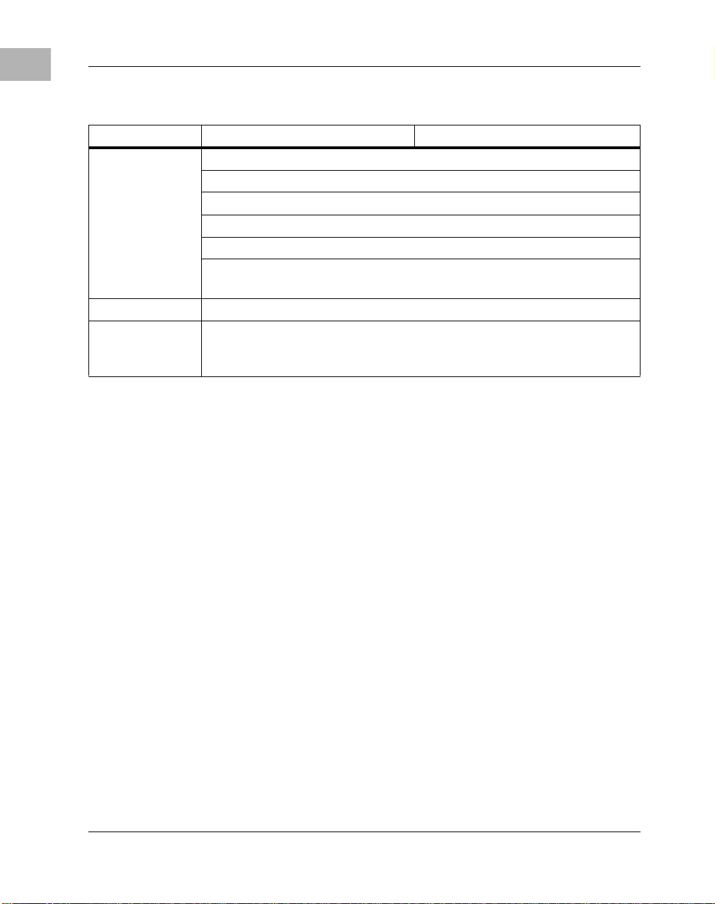
Model Number Characteristics
MVME167PA-24SE 25MHz MC68040, 16MB SDRAM, SCSI and Ethernet
MVME167PA-25SE 25MHz MC68040, 32MB SDRAM, SCSI and Ethernet
MVME167PA-34SE 33MHz MC68040, 16MB SDRAM, SCSI and Ethernet
MVME167PA-35SE 33MHz MC68040, 32MB SDRAM, SCSI and Ethernet
MVME167PA-36SE 33MHz MC68040, 64MB SDRAM, SCSI and Ethernet
MVME177PA-54SE 50MHz MC68060, 16MB SDRAM, SCSI and Ethernet
MVME177PA-55SE 50MHz MC68060, 32MB SDRAM, SCSI and Ethernet
MVME177PA-56SE 50MHz MC68060, 64MB SDRAM, SCSI and Ethernet
MVME177PA-64SE 60MHz MC68060, 16MB SDRAM, SCSI and Ethernet
MVME177PA-65SE 60MHz MC68060, 32MB SDRAM, SCSI and Ethernet
MVME177PA-66SE 60MHz MC68060, 64MB SDRAM, SCSI and Ethernet
MVME177PA-67SE 60MHz MC68060, 128MB SDRAM, SCSI and Ethernet
This manual is intended for anyone who designs OEM systems, adds
capability to an existing compatible system, or works in a lab environment
for experimental purposes. A basic knowledge of computers and digital
logic is assumed. To use this manual, you may also wish to become
familiar with the publications listed in Appendix C, Related
Documentation.
xxi
Page 22

Overview of Contents
Chapter 1, Programming Issues, describes the board-level hardware
features of MVME1X7P single-board computers. It includes memory
maps and a discussion of some general software considerations such as
cache coherency, interrupts, and bus errors.
Chapter 2, VMEchip2, describes the VMEchip2 ASIC, the local
bus/VMEbus interface chip on MVME1X7P boards.
Chapter 3, PCCchip2, describes the PCCchip2 ASIC. The PCChip2 is a
peripheral channel controller designed to interface an MC680x0compatible local bus to va rious on -board periph eral de vices s uch as SCSI
and LAN controllers.
Chapter 4, MCECC Functions, desc ribes the ECC DRAM controlle r ASIC
(MCECC). On the MVME1X7P boa rds, i t sup plies th e interf ace t o a 144 bit wide DRAM memory system.
Appendix A, Summary of Changes, lists the modifications that
accompanied the introduction of the Petra ASIC on the MVME167P and
MVME177P.
Appendix B, Printer and Serial Port Connections, contains drawings of
the printer and serial port interface connections available with the
MVME167P/MVME177P and MVME712 series transition board.
Appendix C, Related Documenta tion, lists all documentation related to the
MVME167P and MVME177P.
Comments and Suggestions
Motorola welcomes and appreciates your comments on its doc umentation.
We want to know what y ou think about our manuals and how we can make
them better. Mail comments to:
Motorola Computer Group
Reader Comments DW164
2900 S. Diablo Way
Tempe, Arizona 85282
xxii
Page 23

You can also submit comments to the following e-mail address:
reader-comments@mcg.mot.com
In all your corres pondence , plea se li st your name, po siti on, and c ompan y.
Be sure to include the title and par t number of the manual and tell how you
used it. Then tell us your feelings about its strengths and weaknesses and
any recommendations for improvements.
Conventions Used in This Manual
The following typographical conventions are used in this document:
$ dollar specifies a hexadecimal number
% percent specifies a binary number
& ampersand specifies a decimal number
Unless otherwise specified, all address references are in hexadecimal.
An asterisk (*) following the signal name for signals which are level
significant denotes that the signal is true or valid when the signal is low.
An asterisk (*) following the signal name for signals which are edge
significant deno tes that the a ctions init iated by th at signal occu r on high to
low transitio n.
xxiii
Page 24

bold
is used for user inpu t that you t ype just as i t appears ; it is al so used for
commands, options and arguments to commands, and names of
programs, directories and files.
italic
is used for names of variables to which you assign values. Italic is also
used for comments in screen dis plays and examples, and to introduce
new terms.
courier
is used for system output (for example, screen displays, reports),
examples, and system prompts.
<Enter>, <Return> or <CR>
<CR> represents the carriage return or Enter key.
CTRL
represents the Control key. Execute control character s by pressing the
Ctrl key and the letter simultaneously, for example, Ctrl-d.
In this manual, assertion and negation are used to specify forcing a signal
to a particular stat e. In parti cular, a ssertion and asser t refe r to a signal tha t
is active or true; negation and negate indicate a signal that is inactive or
false. These terms ar e used independently of the vo ltage level (high or l ow)
that they represent.
xxiv
Data and address sizes are defined as follows:
❏ A byte i s eight bits, numb ered 0 through 7, wit h bit 0 being the leas t
significant.
❏ A word is 16 bits, numbered 0 th rough 15, wit h bit 0 bei ng the le ast
significant.
❏ A longword is 32 bi ts, numbered 0 through 31, with bit 0 being the
least significant.
Page 25

The terms control bit, status bit, true, and false are used ext ensively in this
document. The term control bit is used to describe a bit in a register that
can be set and cleared under software control. The term true is use d to
indicate that a bit is in the state that enables the function it controls. The
term false is used to indicate that the bit is in the state that disables the
function it controls. In all tables, the terms 0 and 1 are used to describe the
actual value that sh ould be written to the bit, or the value that it yields when
read. The term status bit is used to describe a bit in a regi ster that reflects
a specific condition. The status bit can be read by software to determine
operational or exception conditions.
xxv
Page 26

xxvi
Page 27

Introduction
The MVME167P and MVME177P single-board computers are complex
boards that interface both to the VMEbus and the SCSI bus. From a
programming standpoint, their multiple-bus interfaces raise issues of
cache coherency and support of indivisible cycles. There are also various
potential sources of bus error.
This chapter discusses those topics in addition to interrupt handling, the
use of bus timers, and the programming interface to each device on the
board. Programmable regist ers that reside in ASICs (Applicati on-Specific
Integrated Circuit s) on the MVME1X7P boards are covered in the chapters
devoted to those devices.
Note The MVME1X7P’s new ’‘Petra’’ ASIC performs the functions
1Programming Issues
1
previously implemented in the MCECC chip. For ease of use in
conjunction with programming models and documentation
developed for earlier boards, however, the structure of this
manual preserves the functional distinctions that formerly
characterized the MCECC ASIC.
The Petra ASIC and Second-Generation MVME1X7 Boards
Due to rapid changes in tec hnology, the productio n of certain ASI Cs used
on various Motorola first- and second-generation VME embedded
controllers and single-board computers has ended. The Petra chip was
developed to replace these discontinued ASICs. In the case of
MVME167/177 series boards, the di scontinue d ASIC is the MCECC chip.
The Petra chip now suppl ies the functi ons formerly implemented in the
MCECC chip.
1-1
Page 28

1
Programming Issues
The Petra ASIC is functionally compatible with each of the components
that it replaces. In cases where functionality between ASICs is exclusive,
configuration switches or jumpers are provided to let you select the
desired functionality.
In several areas of functionality, the configuration switches provide
backward compatibilit y with earl ier MVME167/17 7 implement ations, but
you can override their settings in software if you wish. A “R/W” by the
corresponding regi ster table entry in this manual denotes inst ances where
this override capability is present.
Where the older technology supported “fast page” or “EDO” DRAM
chips, the Petra memory controllers support SDRAM devices. The two
memory controllers modeled in Petra duplicate the functionality of the
“parity” memory control ler f ound i n the MC ASICs used o n cert ain ot her
boards as well as th at of the “single-bit error correcting/double-bit er ror
detecting” memory controller found in the MCECC ASICs used on the
MVME167/177.
This Programmer’s Reference Guide describes the MCECC model (in
Chapter 4). In the MVME167/177 application, there is logic on the Petra
chip to prevent you from in advertently enabling the MC memory controller
model.
The same SDRAM memory array serves both controller models. The
SDRAM array is 32 data bits wi de with 7 checkbits. Th e array architecture
is a non-interleaved single bank for sizes below 32MB. For array sizes
above 32MB, additional physical memory banks are added but the
architecture remains non-interleaved.
A final note on the SDRAM implementation: The bandwidth between the
SDRAM and local bus is greater than it was wit h the earlier DRAM array.
As a result, software takes less time to execute. Applicatio ns that
incorporate elapsed-time functions which are dependent on code
execution may have problems.
For readers who need to know the ASIC-specific differences between the
previous MCECC and Petra/MCECC programming models in detail,
certain areas of the text in this manual are printed in italics and marked
with change bars (as is done her e). Readers should compare those sections
to the corresp onding se ctions o f the first - and s econd-g eneration manuals.
1-2 Computer Group Literature Center Web Site
Page 29

Introduction
Features
The “Petra” ASIC supplants the MCECC memory controller ASIC on
MVME1X7P boards, performin g the memory control func tions previously
carried out by the MCECC chip: It supplies the programmable int erface for
the ECC-protected 16/32/64/128MB DRAM emulation.
The following table summarizes the features of the MVME167P and
MVME177P single-board computers.
Table 1-1. MVME1X7P Features Summary
Feature MVME167P MVME177P
Processor 25/33MHz 32-bit MC68040
microprocessor
DRAM 16/32/64/128MB synchro nous DRAM (SDRAM). Configu rable to emulate
4/8/16/32/64/128MB ECC-protected DRAM
MVME1X7P boards use SDRAM (Synchr onous DRAM ) in place of DRAM.
Up to 64MB SDRAM is available on MVME167P boards; up to 128MB is
available on MVME177P boards.
SRAM 128KB SRAM with battery backup
EPROM Four 44-pin JEDEC standard PLCC
EPROM sockets
Flash Not available Four Intel 28F008SA Flash memory
NVRAM and
RTC
Timers Four 32-bit tick timers and watchd og timer in Petra ASIC
Software
Interrupts
I/O Four EIA-232-D configurable serial ports via P2 and transition module
8K by 8 Non-Volatile RAM (NVRAM) and Real-Time Clock (RTC) with
battery backup and watchdog function (SGS-Thomson M48T58)
Two 32-bit tick timers and watchdog timer in VMEchip2 ASIC
Eight software interrupts (including those in the VMEchip2 ASIC)
Parallel (printer) interface via P2 and transition module
SCSI interface with DMA via P2 or LCP2 adapter board
Ethernet transceiver interface via DB15 connector on transition module
50/60MHz 32-bit MC68060
microprocessor
Two 44-pin JEDEC standard PLCC
EPROM sockets
devices with optional write protection
1
http://www.motorola.com/computer/literature 1-3
Page 30
1
Programming Issues
Table 1-1. MVME1X7P Features Summary (Continued)
Feature MVME167P MVME177P
VMEbus
interface
Switches Two pushbutton switches
Status Indicators Eight LEDs: Board Fail (FAIL), CPU Status (STAT), CPU Activity (RUN),
VMEbus system controller functions
VMEbus-to-local-bus interface (A32/A24, D32/D16/D8)
Local-bus-to-VMEbus interface (A16/A24/A32, D8/D16/D32)
Programmable interrupter and interrupt handler
Global Control/Status register for interprocessor communications
DMA capability for fast local-memory/VMEbus trans f ers (A16/A24/A32,
D16/D32 (D16/D32/D64 BLT)
(ABORT and RESET)
System Controller (
Activity
(SCSI), VME Activity (VME)
SCON), LAN Activity (LAN), LAN Pow er ( +12V), SCSI
Applicable Industry Standards
These boards conform to the requirements of the following documents:
❏ VMEbus Specification (IEEE 1014-87)
❏ EIA-232-D Serial Interface Specification, EIA
❏ SCSI Specification, ANSI
Block Diagram
Figure 1-1 and Figure 1- 2 ar e ge neral block diagrams of the MVME167P
and MVME177P single-board computers.
1-4 Computer Group Literature Center Web Site
Page 31

Introduction
1
Memory Array
ECC SDRAM
16-64MB
Up to 128MB ECC DRAM
Battery Optio n
MPU
SRAM
MC68040
PETRA
Connectors
Mezzanine
VMEchip 2
Interface
128KB
25/33MHZ
PCCCHIP 2
VMEbus
4 44-pin
PLCC
Controller
Ethernet
Compressor
SCSI
I/O Controller
Quad Serial
EPROM
i82696CA
53C710
CD2401
P1
P2
8KB RAM/Clock
Battery Backed
M48T58
Compatible
Parallel I/O
Centronics
Port
2816 0800
Figure 1-1. MVME167P Block Diagram
http://www.motorola.com/computer/literature 1-5
Page 32

1
Programming Issues
Memory Array
ECC SDRAM
16-128MB
Up to 128MB ECC DRAM
Battery Optio n
MPU
SRAM
4MB FLASH PETRA
MC68040
Connectors
Mezzanine
VMEchip 2
Interface
128KB
50/60MHZ
PCCCHIP 2
VMEbus
2 44-pin
PLCC
Controller
Ethernet
Compressor
SCSI
I/O Controller
Quad Serial
EPROM
i82696CA
53C710
CD2401
P1
P2
8KB RAM/Clock
Battery Backed
M48T58
Compatible
Parallel I/O
Centronics
Port
2816 0800
Figure 1-2. MVME177P Block Diagram
1-6 Computer Group Literature Center Web Site
Page 33

Programming Interfaces
The following sections describe the programming interface to devices on
the MVME167P and MVME177P single-board computers. Unless the
section specifies a particular board type, the discussion applies to both
models.
MC680X0 MPU
The MVME167P is based on the MC68040 microprocessor. The
MVME177P is based on the MC68060 microprocessor. Both processors
have on-chip instruction and data caches and a floating-point processor
(refer to the MC68040 and MC68060 user’s manuals for more
information).
Both models are available in various versions with the features listed in
Table 1-1 on page 1-3.
Data Bus Structure
Programming Interfaces
1
The local bus for all si ngl e-board computers described in this manual is a
32-bit synchronous bus, which is based on an MC68040-compatible bus
and which supports burst transfers. Throughout this manual this bus is
referred to as the Local Bus. The various Local Bus master and slave
devices use the Local Bus to c ommunicate. Th e Local Bus is arbi trated b y
priority type a rbiter. The pr iority o f the Loca l Bus ma sters fr om highe st to
lowest is:
Highest priority 82596CA LAN
CD2401 serial (through the PCCchip2)
53C710 SCSI
VMEbus
Lowest priority MPU
http://www.motorola.com/computer/literature 1-7
Page 34

1
Programming Issues
As a general rule, any master can access any slave; not all combinations
pass the common sense test, h owever. Refer to the device- specific sectio ns
of this manual and t o the us er’s guide for eac h de vice t o deter min e its port
size, data bus connection, and any restrictions that apply when accessing
the device.
EEPROMs on the MVME1X7P
Both boards include 44-pin PLCC/CLCC sockets for EEPROMs,
organized as follows:
Model Sockets Banks
MVME167 4 2
MVME177 2 1
The MVME167P boards use 27C102JK or 27C202JK type EEPROMs.
The MVME177 boards use SGS-Thompson M27C4002 (256K x 16) or
AMD 27C4096 type EEPROMs.
The EEPROMs are organized as 32-bit wide banks that support 8-, 16-,
and 32-bit read accesses. (The MVME177 has Flash memory in addition
to EEPROM.)
MVME167
The EEPROMs are mapped to Local Bus addres s 0 following a Local Bus
reset. This allows t he MC6 8040 to access the stack pointer and exec uti on
address following a reset. The EEPROMs are contr olled by the VMEchip2
ASIC. The map decoder, the access time, and the time they appear at
address 0 are programmable parameters. Refer to Chapter 2, VMEchip2 for
more detail.
1-8 Computer Group Literature Center Web Site
Page 35

MVME177
The EEPROMs on the MVME177 share 2MB of memory with the first
2MB of Flash memory. The EEPROM can co-exist with 2MB of Flash, or
you may wish to program all 4MB as Flash memory. The Flash and
EEPROM configuration is jointly controlled by a configuration switch
(S4) as described in Chapters 1 and 4 of MVME177P Single Board
Computer Installation and Use, and by control bit GPIO2 in the
VMEchip2 ASIC, as described in Chapter 2, VMEchip2.
The EPROMs are mapped to Local Bus address 0 following a Local Bus
reset.This allows the MC68060 processor to access the reset vector and
execution address following a reset.
Flash Memory on the MVME177
The MVME177 includes four 28F008SA Flash memory devices. The 32bit wide Flash can support 8-, 16-, and 32-bit accesses. The Flash can be
used for the onboard debugger firmware, which can be downloaded from
I/O resources such as Ether net, SCSI, serial port, or VMEbus . Flash writeprotection is programmable by setting a control bit (GPIO bit 1) in the
VMEchip2 GPIO register after downloading.
Programming Interfaces
1
When the Flash memory is used with EEPROM, only the top or bottom
2MB of Flash memory is visible at any one time. For access to the
shadowed area of Flash, the 177Bug firmware provides the SFLASH
command.
The MVME177 is shipped with the top 2MB of Flash memory and
EEPROM mapped as illustrated by Map 2 in Figure 1-3.
The 177Bug is shipped in EEPROM. To map all 4MB of Flash and retain
access to the 177Bug, perform the following steps:
1. Map Flash and EEPROM as shown in Map 3 in Figure 1-3.
2. Copy the 177Bug into the bottom 2MB of Flash memory.
3. Remap Flash memory as shown in Map 1 in Figure 1-3.
http://www.motorola.com/computer/literature 1-9
Page 36

1
Programming Issues
MAP 1
FFBFFFFF
FLASH
MEMORY
4MB
FF800000
NO EPROM
IN MAP
MAP 2
(as shipped)
FLASH
TOP 2MB
1MB EPROM
DUPLICATED:
READABLE
NOT WRITABLE
1MB EPROM
(BUG)
MAP 3
FLASH
BOTTOM
2MB
1MB EPROM
DUPLICATED:
READABLE
NOT WRITABLE
1MB EPROM
FFBFFFFF
FFA00000
FF900000
FF800000
1534 9408
Figure 1-3. MVME177 Flash and EPROM Memory Mapping Schem es
SRAM
The MVME167P and MVME177P single-board computers include
128KB of 32-bit wide 100ns static RAM (SRAM) that supports 8-, 16-,
and 32-bit wide accesses. The SRAM allows the debugger to operate and
limited diagnostics to execute without using the on-board SDRAM or
mezzanines. The SRAM is under t he cont rol o f the VMEchip2 ASI C, and
the access time is progr ammable. Refer to Chapter 2, VMEchip2 for more
detail.
The MVME177P provides for SRAM battery bac kup. The battery backup
function is supplied by a Dallas DS1210S nonvolatile controller chip and
Panasonic 2032 (or equivalent) battery.
1-10 Computer Group Literature Center Web Site
Page 37

The MVME177P implements primary a nd secondary backup sources. You
can select from +5V standby power, the onboard battery, or both.
The jumpers and configuration switches for the MVME167P and
MVME177P are described in Chapter 1 of the Installation and Use manual
for the respective boards.
Onboard SDRAM
MVME167P boards are built with 16MB-64MB synchronous DRAM
(SDRAM). MVME177P boards are built with 16MB-128MB SDRAM.
The MVME1X7P may have the SDRAM configured to model 4MB, 8MB,
16MB, 32MB, 64MB, or 128MB of ECC-protected DRAM.
In addition to the onboard SDRAM, an additional mezzanine (of the type
used on previous MVME1X7 boards) can be plugged in to provide up to
128MB of additional DRAM. All DRAM has ECC protection.
The SDRAM map decoder can be pr ogrammed to acc ommodate di ffer ent
base address(es) and sizes of mezzanine boards. The onboard SDRAM is
disabled by a Local Bus reset; it must be programmed in order for you to
access it.
Programming Interfaces
1
Most DRAM devices require some number of access cycles before the
DRAMs are fully operational. Normally this requirement is met by the
onboard refresh circuitry and normal DRAM initialization. However,
software should insure a minimum of 10 initialization cycles are
performed to each bank of RAM.
Detailed pro gramming informa tion is availab le in the chapte rs on the
memory options.
http://www.motorola.com/computer/literature 1-11
Page 38

1
Programming Issues
Battery-Backed-Up RAM and Clock
Although the M48T58-70 RAM and clock chip is an 8-bit device, the
interface provided by the PCCchip2 supports 8-, 16-, and 32-bit accesses
to the M48T58. No interrupts are generated by the clock. Refer to Chapter
3, PCCchip2 and to the M48T58 data sheet for detailed programming
guidance and battery life information.
VMEbus Interface
The VMEbus interface is implemented with an ASIC called the
VMEchip2. The VMEchip2 includes:
❏ Two tick timers
❏ A watchdog timer
❏ Programmable map decoders for the master and slave interfaces
❏ A VMEbus to/from local bus DMA controller
❏ A VMEbus to/from local bus non-DMA programmed access
interface
❏ A VMEbus interrupter, a VMEbus system controller, a VMEbus
interrupt handler, and a VMEbus requester
Processor-to-VMEbus tra nsfers can be D8, D16, or D32. VMEchip2 DMA
transfers to the VMEbus, however, can be D16, D32, D16/BLT, D32/BLT,
or D64/MBLT.
Refer to Chapter 2, VMEchip2 for detailed programming information.
I/O Interfaces
The MVME167P and MVME177P single-board computers provide
onboard I/O for many syst em applications. The I/O func tions include serial
ports, parallel (printer) port , Ethernet trans ceiver interf ace, and SCSI mass
storage interface.
1-12 Computer Group Literature Center Web Site
Page 39

Serial Port Interface
The CD2401 serial controller chip (SCC) is used to implement the four
serial ports. The ser ial port s support th e standar d baud rate s (110 to 3 8.4K
baud). The four serial ports differ in function because of the limited
number of pins on the P2 I/O connector:
❏ Serial port 1 is a minimum-function asynchronous port. It uses
❏ Serial ports 2 and 3 are full-function asynchronous ports. They use
❏ Serial port 4 is a ful l-functio n asynchron ous or synch ronous port . It
All four serial ports use EIA-232-D drivers and receivers located on the
main board, and all the signal lines are routed to the I/O connector. The
configuration headers are located on the main board and may be on some
transition boar ds. An external I/O transition board is nec ess ary to convert
the I/O connector pinout to industry-standard connectors.
Programming Interfaces
1
RXD, CTS, TXD, and RTS.
RXD, CTS, DCD, TXD, RTS, and DTR.
can operate at synchronous bit rates up to 64 k bits per second. It
uses RXD, CTS, DCD, TXD, RTS, and DTR. It also interfaces to
the synchronous clock signal lines. Refer to Appendix C, Related
Documentation for drawings of the serial port interface
connections.
Note The MVME1X7P board hardware ties the DTR signal from the
CD2401 to the pin labeled RTS at connector P2. Likewise , RTS
from the CD2401 is tied to DTR on P2. Therefore, when
programming the CD2401, assert DTR when you want RTS, and
RTS when you want DTR.
On both MVME167P and MVME177P boards, the interface provided by
the PCCchip2 allows t he 16-b it CD2401 ser ial cont roll er chip t o appear at
contiguous addresses. Acce ss es to the CD2401, howeve r, must be 8 or 16
bits. 32-bit acces ses are not permitted. Ref er to the CD24 01 data sheet and
to Chapter 3, PCCchip2 for detailed pro gramming information.
http://www.motorola.com/computer/literature 1-13
Page 40

1
Programming Issues
The CD2401 supports DMA operations to local memory. Because the
CD2401 does not support a retry operation necessary to break VMEbus
lockup conditions, the CD2401 DMA controllers should not be
programmed to access the VMEbus. The hardware does not restrict the
CD2401 to onboard DRAM.
Parallel (Printer) Interface
The PCCchip2 ASIC provides an 8-bit bidirectional parall el port. All eight
bits of the port must be either inputs or outputs (no individual selection).
In addition to the 8 bits of data, there are two control pins and five status
pins. Each of the status pins can generate an interrupt to the MPU in any
of the following programmable conditions: high level, low level,
high-to-low transit ion, or low-to-h igh transi tion. This po rt may be used as
a Centronics-compatible parallel printer port or as a general parallel I/O
port.
When used as a para llel printer por t, the five stat us pins function as : Printer
Acknowledge (ACK), Printer Fault (FAULT∗), Printer Busy (BSY),
Printer Select (SELECT), and Printer Paper Error (PE), while the control
pins act as P rinter Strobe (STROBE∗), and Input Prime (INP∗).
The PCCchip2 provides an auto-strobe feature similar to that of the
MVME147 PCC. In auto-strobe mode, after a write to the Printer Data
Register, the PCCchip2 automatically asserts the STROBE∗ pin for a
selected time specified by the Printer Fast Strobe control bit. I n manual
mode, the Printer Strobe control bit directly controls the state of the
STROBE∗ pin.
Refer to Chapter 3, PCCchip2 for detailed programming information.
Refer to Appendix C, Relate d Documenta tion for drawings of the printer
port interface connections.
1-14 Computer Group Literature Center Web Site
Page 41

Ethernet Interface
The MVME1X7P uses the Intel 82596CA LAN co processor to implement
the Ethernet transceiver interface. The 82596CA accesses local RAM
using DMA operations to perform its normal functions. Because the
82596CA has small internal buffers and the VMEbus has an undefined
latency period, buffer overrun may occur if the DMA is programmed to
access the VMEbus. Therefore, the 82596CA should not be programmed
to access the VMEbus.
Every MVME1X7P that is built with an Ethernet interface is assigned an
Ethernet Station Addre ss. The add ress i s $0001AFxxxxxx where x xxx xx is
the unique 6-nibble n umber assigned to the board (i.e., every MVME1X7P
has a different value for xxxxxx).
Each board has an Ethernet Station Address displa yed on a label attached
to the VMEbus P2 connector. In addition, the six bytes including the
Ethernet address are s tored in the co nfigurat ion area of the BBRAM. That
is, 0001AFxxxxxx is stored in the BBRAM. At an addre ss of $FFFC1F2 C,
the upper four bytes (0001AFxx) can be read. At an address of
$FFFC1F30, the lower two bytes (xxxx) can be read. (Refer to the
BBRAM/TOD Clock memory map description in this chapter under
Battery-Backed-Up RAM and Clock for specifics.)
Programming Interfaces
1
The MVME1X7P debugger firmware has the capability to retrieve or set
the Ethernet address. If the data in the BBRAM is lost , use the number on
the VMEbus P2 connector label to restore it.
The Ethernet transceiver interface is located on the MVME1X7P main
board, and the industry-standard DB15 connector is located on the
MVME712B transition board.
Support functions fo r the 82596CA LAN co proc essor are p rovide d by th e
PCCchip2 ASIC. Refer to the 82596CA user’s guide and to Chapter 3,
PCCchip2 for detailed programming information.
http://www.motorola.com/computer/literature 1-15
Page 42

1
Programming Issues
SCSI Interface
The MVME167P and MVME177P single-board computers provide for
mass storage subsystems through the industry-standard SCSI bus. These
subsystems may include hard and floppy disk drives, streaming tape
drives, and othe r mass storage devices. The SCSI interface is implemented
using the NCR 53C710 SCSI I/O controller.
Support functions for the 53C710 are provided by the PCCchip2 ASIC.
Refer to the 53C710 user’s guide and to Chapter 3, PCCchip2 for detailed
programming information.
SCSI Termination
It is important that the SCSI bus be properly terminated at both ends.
Sockets for terminators are provided on the P2 or LCP2 adapter board. If
the SCSI bus ends at the adapter board, termination resistors must be
installed on the adapter board. +5V power to the SCSI bus TERM power
line and termination resistors is supplied through a fuse located on the
adapter board (in the case of the MVME167P) or through a fuse on the
MVME712 series transition module and a diode on the adapter board (in
the case of the MVME177P).
Local Resources
The MVME167P and MVME177P single-board computers incl ude many
resources for the local processor. These include tick timers, softwareprogrammable hardware interrupts, a watchdog timer, and a local bus
timeout.
Programmable Tick Timers
Four 32-bit programmable tick timers with 1µs resolution are available:
two in the VMEchip2 ASIC and two in the PCCchip2 ASIC. The tick
timers may be programmed to generate periodic interrupts to the
processor. Refer to Chapter 2, VMEchip2 and Chapter 3, PCCchip2
respectively for detailed programming information.
1-16 Computer Group Literature Center Web Site
Page 43

Watchdog Timer
The VMEchip2 ASIC supplies a watchdog timer fu nction. When enab led,
the watchdog timer must be reset by software within the programmed
interval or it times out. The watchdog timer can be programmed to
generate a SYSRESET∗ signal, a local re set signal , or a board f ail signal if
it times out. Refer to Chapter 2, VMEchip2 for detailed programming
information.
Software-Programmable Hardware Interr upts
The VMEchip2 ASIC supplies eight software-programmable hardware
interrupts. These interrupts allow software to create a ha rdware interrupt.
Refer to Chapter 2, VMEchip2 for detailed programming information.
Local Bus Timeout
The MVME167P and MVME177P single-board computers provide a
timeout function in the VMEchip2 ASIC for the Local Bus. When the
timer is enabled and a Local Bus access times out, a Transfer Error
Acknowledge (TEA) signal is sent to the Local Bu s master. The time -out
value is selectable by software for 8 µsec, 64 µsec, 256 µsec, or infinite.
The Local Bus timer does not operate during VMEbus bound cycles.
Functional Description
1
VMEbus bound cycles are timed by the VMEbus access timer and the
VMEbus global timer. Refer to Chapter 2, VMEchip2 for detailed
programming information.
Functional Description
This section highlights a few specific features of the MVME1X7P singleboard computers. For a complete functional description of the major
blocks of the MVME1X7P, refer to the Installation and Use manual.
http://www.motorola.com/computer/literature 1-17
Page 44

1
Programming Issues
VMEbus Interface and VMEchip2
The local-bus-to-VMEbus interface and the VMEbus-to-local-bus
interface are provided by the VMEchip2 ASIC. The VMEchip2 can also
provide the VMEbus system cont roll er func tions . Refer t o the VMEchi p2
description in Chapter 2 for detailed programming information.
VMEchip2 General-Purpose I/O
The MVME1X7P single-board computers, both MVME167P and
MVME177P, follow the previous MVME177 in their routing of GPIO
signals:
❏ GPIO1 controls Flash memory w rite protection.
❏ GPIO3 selects between shared EPROM/Flash mode or Flash-only
mode.
❏ GPIO2 controls whether the upper or lower Flash addres ses are used
in shared EPROM/Flash mode.
❏ GPIO0’s function as +12V power status signal is unchanged.
Petra/VMEchip2 Redundant Logic
In support of possible future configurations in which the MVME1X7P
might be offered as a single-board computer without the VMEbus
interface, certain logic in the VMEchip2 has been duplicated in the Petra
chip. Table 1-2 shows the location of the overla pping logic. As long as the
VMEchip2 ASIC is present, the redundant logic is inhibited in the Petra
chip.
Note that the
ABORT switch logic in the VMEchip2 is not used. Likewise
unused are the GPI inputs to the VMEchip2, which are located at
$FFF40088 bits 7-0. Ins tead, the
ABORT switch interrupt is integrated into
the Petra ASIC at l ocat ion $FFF 42043. Th e GPI inpu ts ar e int egrat ed i nto
the Petra ASIC at location $FFF4202C bits 23-16.
1-18 Computer Group Literature Center Web Site
Page 45

Functional Description
Table 1-2. Functions Duplicated in VMEchip2 and Petra ASICs
1
VMEchip2 Petra Chip
Address Bit # Address Bit #
$FFF40060 28-24 $FFF42044 28-24 1,5
$FFF40060 22-19,
17,16
$FFF4004C 13-8 $FFF42044 13-8 3,5
$FFF40048 7 $FFF42048 8 4
$FFF40048 9 $FFF42048 9 4,5
$FFF40048 10 $FFF42048 10 4,5
$FFF40048 11 $FFF42048 11 4,5
$FFF40064 31-0 $FFF4204C 3-0 8
$FF800000-$FFBFFFFF 31-0 $FF800000-$FFBFFFFF 31-0 7
$FFE00000-$FFEFFFFF 31-0 Programmable 31-0 7
$FFF42044 22-19,
17,16
$FFF42040 6- 0 6
Notes
2,5
Notes
RESET switch control.
1.
2. Watchdog ti mer control.
3. Access and watchdog timer parameters.
4. MPU TEA (bus error) status
5. Bit numbering for the VMEchip2 and Pet ra ASICs has a one-to-one
correspondence.
ABORT switch interrupt control. Implemented also in the
6.
VMEchip2, but with a different bit organization (refer to the
VMEchip2 description in Chapter 2). In the MVME1X7P, the
ABORT switch is wired to the Petra chip, not the VMEchip2.
7. The SRAM and EPROM decoder in the VMEchip2 (ve rsion 2) must
be disabled by software before any accesses are made to these
address spaces.
http://www.motorola.com/computer/literature 1-19
Page 46

1
Programming Issues
8. 32-bit prescaler. The prescaler can also be accessed at $FFF40064
when the optional VMEbus is not enabled.
Memory Maps
There are two points of view for memory maps:
1. The mapping of all resources as viewed by local bus masters (local
bus memory map)
2. The mapping of onboard resources as viewed by VMEbus masters
(VMEbus memory map)
The memory maps and I/O maps described in the following tables are
correct for all l ocal bus masters. Some add ress translati on capability exi sts
in the VMEch ip2. This capab ility makes it pos sible to have multiple
MVME1X7P modules on the same VMEbus with different virtual local
bus maps as viewed by different VMEbus masters.
Local Bus Memory Map
The local b us memory map is split into different addr ess spaces by the
transfer type (TT) signals. The local resources respond to the normal
access and interrupt acknowledge codes.
Normal Address Range
The following tables show t he memory maps of devices that res pond to the
normal address range . The normal addr ess range is def ined by the Tra nsfer
Type (TT) signals on the local bus. On the MVME1X7P, Transfer Types
0, 1, and 2 define the normal address range.
Table 1-3 is the entire map from $00000000 to $FFFFFFFF. Many areas
of the map are user-programmable, and suggested uses are shown in the
table. The cache in hibit funct ion is prog rammable in the MC680 x0 MMU.
1-20 Computer Group Literature Center Web Site
Page 47

Memory Maps
The onboard I/O space must be marked cache-inhibit and serialized in its
page table. Table 1-4 on page 1-22 furth er defines the map for the local I/O
devices on the MVME1X7P.
Table 1-3. Local Bus Memory Map
1
Address
Range
$00000000 DRAMSIZE
DRAMSIZE $FF7FFFFF
$FF800000 $FFBFFFFF
$FFC00000 $FFDFFFFF
$FFE00000 $FFE1FFFF
$FFE20000 $FFEFFFFF
$FFF00000 $FFFEFFFF
$FFFF0000 $FFFFFFFF
Software
Devices Accessed Port Size Size
User Programmable
(Onboard SDRAM)
User Programmable
(VMEbus)
ROM (167P) D32 4MB N 1
EPROM/Flash (177P) D32
Reserved -- 2MB -- 5
SRAM D32 128KB N --
SRAM (repeated) D32 896KB N --
Local I/O Devices
(Refer to next table)
User Programmable
(VMEbus A16)
D32
D32/D16 3GB ? 3, 4
D32-D8 1MB Y 3
D32/D16 64KB ? 2, 4
DRAMSIZE
2MB
EPROM,
4MB Flash
Cache
Inhibit
N1, 2
N1,6
Notes
Notes
1. ROM on MVME167P, ROM/Flash on MVME177P. Flash/EPROM
devices appear at $FF800000 - $FFBFFFFF, and also appear at
$00000000 - $003FFFFF if the ROM0 bit in the VMEchip2
EPROM control register is high (ROM0 = 1).
The ROM0 bit is located at address $FFF40 030 bit 20. ROM0 is set
to 1 after each reset. The ROM0 bit must be cleared before other
resources (DRAM or SRAM) can be mapped in this range
http://www.motorola.com/computer/literature 1-21
Page 48

1
Programming Issues
($00000000 - $003FFFFF). The VMEchip2 and DRAM map
decoders are disabled by a local bus reset.
On the MVME177P, the Flash/EPROM memory is mapped at
$00000000 - $003FFFFF by hardware default through the
VMEchip2.
2. This area is user-pro gram mable. The sugges ted u se is shown i n the
table. The DRAM decoder is progr ammed in the MCECC chi p, and
the local-to-VMEbus decoders are programmed in the VMEchip2.
3. Size is approximate.
4. Cache inhibit depends on devices in area mapped.
5. This area is not decoded. If these locations are accessed and the
local bus timer is enabled, the cycle times out and is terminated by
a TEA signal.
6. The Flash and EEPROM configuration is jointly controlled by a
configuration switch (S4) as described in Chapters 1 and 4 of
MVME177P Single Board Computer Installation and Use, and by
control bit GPIO2 in the VMEchip 2 ASIC, as de scrib ed in Chapt er
2, VMEchip2. Depending on the setting of S4, this address space
may reference 2MB EPROM, 1MB EPROM and 2MB Flash, or
4MB Flash.
Table 1-4 focuses on the Local I/O Devices portion of the local bus Main
Memory Map..
Table 1-4. Local I/O Devices Memory Map
Address Range Devices Accessed Port Size Size Notes
$FFF00000 - $FFF3FFFF Reserved -- 256KB 5
$FFF40000 - $FFF400FF VMEchip2 (LCSR) D32 256B 1,4
$FFF40100 - $FFF401FF VMEchip2 (GCSR) D32-D8 256B 1,4
$FFF40200 - $FFF40FFF Reserved -- 3.5KB 5,7
$FFF41000 - $FFF41FFF Reserved -- 4KB 5
$FFF42000 - $FFF42FFF PCCchip2 D32-D8 4KB 1
$FFF43000 - $FFF430FF Petra/MCECC #1 D8 256B 1
1-22 Computer Group Literature Center Web Site
Page 49

Memory Maps
Table 1-4. Local I/O Devices Memory Map (Continued)
Address Range Devi ces Access e d Port Size Size Notes
$FFF43100 - $FFF431FF Petra/MCECC #2 D8 256B 1
$FFF43200 - $FFF43FFF Petra/MCECCs (repeated) -- 3.5KB 1,7
$FFF44000 - $FFF44FFF Reserved -- 4KB 5
$FFF45000 - $FFF451FF CD2401 (Serial Comm. Cont.) D16-D8 512B 1,9
$FFF45200 - $FFF45DFF Reserved -- 3KB 7,9
$FFF45E00 - $FFF45FFF Reserved -- 512B 1,9
$FFF46000 - $FFF46FFF 82596CA (LAN) D32 4KB 1,8
$FFF47000 - $FFF47FFF 53C710 (SCSI) D32/D8 4KB 1
$FFF48000 - $FFF4FFFF Reserved -- 32KB 5
$FFF50000 - $FFF6FFFF Reserved -- 128KB 5
$FFF70000 - $FFF76FFF Reserved -- 28KB 6
$FFF77000 - $FFF77FFF Reserved -- 4KB 2
$FFF78000 - $FFF7EFFF Reserved -- 28KB 6
$FFF7F000 - $FFF7FFFF Reserved -- 4KB 2
$FFF80000 - $FFF9FFFF Reserved -- 128KB 6
$FFFA0000 - $FFFBFFFF Reserved -- 128KB 5
$FFFC0000 - $FFFCFFFF M48T58 (BBRAM, TOD
Clock)
$FFFD0000 - $FFFDFFFF Reserved -- 64KB 5
$FFFE0000 - $FFFEFFFF Reserved -- 64KB 2
D32-D8 64KB 1
1
http://www.motorola.com/computer/literature 1-23
Page 50

1
Programming Issues
Notes
1. For a complete desc ription of the r egister bits, r efer to the data s heet
for the specific chip. For a more detailed memory map refer to the
following detailed peripheral device memory maps.
2. On the MVME1X7P, this area does not return an acknowledge
signal. If the local bus timer is enabled, the access times out and is
terminated b y a TEA signal.
3. Byte reads should be used to read the interrupt vector. These
locations do not respond when an interrupt is not pending. If the
local bus timer is enabled, th e access times out and is ter minated by
a TEA signal.
4. Writes to the LCSR in the VMEchip2 must be 32 bits. LCSR writes
of 8 or 16 bits terminate with a TEA signal . Writes to the GCSR may
be 8, 16 or 32 bits. Reads to the LCSR and GCSR may be 8, 16 or
32 bits.
5. This area does not return an acknowledge signal. If the local bus
timer is enabled, the access times out and is terminated by a TEA
signal.
6. This area does return an acknowledge signal.
7. Size is approximate.
8. Port commands to the 82596CA must be written as two 16-bit
writes: upper word first and lower word second.
9. The CD2401 appears repeatedly from $FFF45200 to $FFF45FFF
on the MVME1X7P. If the local bus timer is enabled, the access
times out and is terminated by a TEA signal.
1-24 Computer Group Literature Center Web Site
Page 51

Detailed I/O Memory Maps
Tables 1-5 through 1-14 give the detailed memory maps for: 7
VMEchip2 Table 1-5
PCCchip 2 Table 1 -7
Printer Table 1-6
MCECC Internal Register Table 1-8
Cirrus Logic CD2401 Serial Port Table 1-9
82596CA Ethernet LAN chip Table 1-10
53C710 SCSI chip Table 1-11
M48T58 BBRAM, TOD Clock Table 1-12
BBRAM Configuration Area Table 1-13
TOD Clock Table 1-14
You can obtain manufacturers’ errata sheets for the various chips listed
above by contacting your local Motorola sales representative. A nondisclosure agreement may be necessary.
Memory Maps
1
http://www.motorola.com/computer/literature 1-25
Page 52

1
Programming Issues
Table 1-5. VMEchip2 Memory Map (Sheet 1 of 3)
VMEchip2 LCSR Base Address = $FFF40000
OFFSET:
16171819202122232425262728293031
0
SLAVE ENDING ADDRESS 1
10
14
18
1C
20
24
28
2C
30
34
38
4
8
C
ADDER
2
SLAVE ENDING ADDRESS 2
SLAVE ADDRESS TRANSLATION ADDRESS 1
SLAVE ADDRESS TRANSLATION ADDRESS 2
SNP
2
WP2SUP2USR2A322A24
BLK
BLK2PRGM2DATA
D64
2
2
2
16171819202122232425262728293031
MASTER ENDING ADDRESS 1
MASTER ENDING ADDRESS 2
MASTER ENDING ADDRESS 3
MASTER ENDING ADDRESS 4
MASTER ADDRESS TRANSLATION ADDRESS 4
MAST
D16
EN
MAST
WP
EN
GCSR GROUP SELECT
MAST
MAST
D16
WP
EN
EN
BOARD SELECT
GCSR
MASTER AM 3MASTER AM 4
MAST
MAST
MAST
4
3
EN
EN
MAST
2
1
EN
EN
16171819202122232425262728293031
WAIT
RMW
ROM
ZERO
DMA TB
SNP MODE
SRAM
SPEED
DMA CONTROLLER
3C
40
44
48
TICK
2/1
TICK
IRQ 1
EN
CLR
IRQ
IRQ
STAT
VMEBUS
INTERRUPT
LEVEL
VMEBUS INTERRUPT VECTOR
DMA CONTROLLER
DMA CONTROLLER
DMA CONTROLLER
This sheet continues on facing page.
1-26 Computer Group Literature Center Web Site
Page 53

ADDER
MAST
MAST
WP
D16
EN
IO2ENIO2
ARB
ROBN
DMA
TBL
INT
EN
WP
EN
MAST
DHB
DMA LB
SNP MODE
IO2
S/U
MAST
DWB
MASTER AM 2 MASTER AM 1
IO2
IO1ENIO1
P/D
MST
FAIR
DMA
INC
VME
LOCAL BUS ADDRESS COUNTER
SLAVE STARTING ADDRESS 1
SLAVE STARTING ADDRESS 2
SLAVE ADDRESS TRANSLATION SELECT 1
SLAVE ADDRESS TRANSLATION SELECT 2
SNP
1
1
WP1SUP1USR1A321A24
MASTER STARTING ADDRESS 1
MASTER STARTING ADDRESS 2
MASTER STARTING ADDRESS 3
MASTER STARTING ADDRESS 4
MASTER ADDRESS TRANSLATION SELECT 4
MAST
MAST
WP
D16
EN
D16
EN
MST
RWD
DMA
INC
LB
IO1
WP
EN
MASTER
VMEBUS
DMA
WRT
IO1
S/U
DMA
D16
EN
DMA
HALT
DMA
D64
BLK
ROM
SIZE
DMAENDMA
DMA
BLK
ROM BANK B
TBL
DMA
AM
5
1
SPEED
DMA
FAIR
DMA
AM
4
BLK
BLK1PRGM1DATA
D64
1
DM
RELM
DMA
DMA
AM
AM
3
Memory Maps
ROM BANK A
SPEED
DMA
VMEBUS
DMA
AM
2
1
DMA
AM
1
0123456789101112131415
1
0123456789101112131415
0123456789101112131415
0
VMEBUS ADDRESS COUNTER
BYTE COUNTER
TABLE ADDRESS COUNTER
MPU
MPU
MPU
MPU
MPU
DMA
DMA
DMA
DMA
DMA
DMA
DMA TABLE
INTERRUPT COUNT
CLR
STAT
LBE
ERR
LPE
ERR
LOB
ERR
LTO
ERR
LBE
ERR
LPE
ERR
LOB
ERR
LTO
ERR
TBL
ERR
VME
ERR
DMA
DONE
1360 9403
This sheet begins on facing page.
http://www.motorola.com/computer/literature 1-27
Page 54

1
Programming Issues
Table 1-5. VMEchip2 Memory Map (Sheet 2 of 3)
VMEchip2 LCSR Base Address = $FFF40000
OFFSET:
4C
50
ARB
BGTO
EN
DMA
TIME OFF
DMA
TIME ON
TICK TIMER 1
VME
GLOBAL
TIMER
16171819202122232425262728293031
54
58
5C
60
64
68
6C
70
74
78
7C
80
84
88
8C
SCON BRD
AC
AB
FAIL
IRQ
IRQ
EN
EN
IRQ
IRQ
31
30
CLR
CLR
IRQ
IRQ
31
30
VECTOR BASE
REGISTER 0
SYS
FAIL
SYS
FAIL
IRQ
EN
IRQ
29
CLR
IRQ
29
AC FAIL
IRQ LEVEL
VME IACK
IRQ LEVEL
SW7
IRQ LEVEL
SPARE
IRQ LEVEL
FAIL
STAT
MWP
BERR
IRQ
EN
IRQ
28
CLR
IRQ
28
PURS
STAT
PE
IRQ
EN
IRQ
27
CLR
IRQ
27
CLR
BRD
PURS
FAIL
STAT
OUT
IRQ1E
TIC2
IRQ
IRQ
EN
EN
IRQ
IRQ
26
25
CLR
CLR
IRQ
IRQ
26
25
ABORT
IRQ LEVEL
DMA
IRQ LEVEL
SW6
IRQ LEVEL
VME IRQ 7
IRQ LEVEL
VECTOR BASE
REGISTER 1
RST
SW
TIC1
IRQ
IRQ
CLR
IRQ
EN
EN
24
24
SYS
RSTWDCLR
VME
IACK
IRQ
EN
IRQ
23
CLR
IRQ
23
MST
IRQ
EN
LEVEL
TO
DMA
IRQ
EN
IRQ
CLR
IRQ
SYS
FAIL
22
22
WD
CLR
CNT
SIG3
IRQ
EN
IRQ
21
CLR
IRQ
21
SYS FAIL
IRQ LEVEL
SIG 3
IRQ LEVEL
SW5
IRQ LEVEL
VME IRQ 6
IRQ LEVEL
AC
FAIL
LEVEL
WD
TO
STAT
SIG2
IRQ
EN
IRQ
20
CLR
IRQ
20
ABORT
LEVEL
TO
BF
EN
SIG1
IRQ
EN
IRQ
19
CLR
IRQ
19
TICK TIMER 1
TICK TIMER 2
TICK TIMER 2
WD
SRST
RST
LRST
SIG0
IRQ
EN
IRQ
18
CLR
IRQ
18
MST WP ERROR
IRQ LEVEL
SIG 2
IRQ LEVEL
SW4
IRQ LEVEL
VME IRQ 5
IRQ LEVEL
GPIOEN
WD
ENWDEN
LM1
IRQ
EN
IRQ
17
CLR
IRQ
17
PRE
16171819202122232425262728293031
LM0
IRQ
EN
IRQ
16
CLR
IRQ
16
This sheet continues on facing page.
1-28 Computer Group Literature Center Web Site
Page 55

Memory Maps
1
VME
ACCESS
TIMER
LOCAL
BUS
TIMER
COMPARE REGISTER
COUNTER
COMPARE REGISTER
COUNTER
OVERFLOW
COUNTER 2
SCALER
SW7
SW6
IRQ
EN
IRQ
SET
IRQ
CLR
IRQ
14
14
14
P ERROR
IRQ LEVEL
IRQ LEVEL
IRQ LEVEL
VME IRQ 4
IRQ LEVEL
GPIOO
SW5
IRQ
EN
IRQ
13
SET
IRQ
13
CLR
IRQ
13
SIG 1
SW3
IRQ
EN
IRQ
SET
IRQ
CLR
IRQ
15
15
15
SW4
IRQ
IRQ
SET
IRQ
CLR
IRQ
0123456789101112131415
TIME OUT
SELECT
CLR
OVF
2
WD
COC
EN
TIC
EN
2
2
OVERFLOW
COUNTER 1
PRESCALER
CLOCK ADJUST
CLR
OVF
TIC
COC
EN
EN
1
1
1
0123456789101112131415
SW3
SW2
SW1
SW0
IRQ
IRQ
IRQ
EN
EN
EN
IRQ
12
11
SET
IRQ
12
11
CLR
IRQ
12
11
EN
IRQ
IRQ
10
9
SET
SET
IRQ
IRQ
10
9
CLR
CLR
IRQ
IRQ
10
9
IRQ1E
IRQ LEVEL
SIG 0
IRQ LEVEL
SW2
IRQ LEVEL
VMEB IRQ 3
IRQ LEVEL
GPIOI GPI
IRQ
IRQ
SET
IRQ
CLR
IRQ
EN
8
8
8
SPARE VME
EN
IRQ
7
MP
IRQ
EN
IRQ7
EN
IRQ
6
REV
EROM
VME
IRQ6
EN
IRQ
5
TIC TIMER 2
IRQ LEVEL
LM 1
IRQ LEVEL
SW1
IRQ LEVEL
VME IRQ 2
IRQ LEVEL
DIS
SRAM
VME
IRQ5
EN
IRQ
DIS
MST
VME
VME
VME
IRQ4
IRQ3
EN
EN
IRQ
3
NO
EL
BBSY
IRQ
2
TIC TIMER 1
DIS
BSYTENINT
4
IRQ2
EN
IRQ
1
IRQ LEVEL
LM 0
IRQ LEVEL
SW0
IRQ LEVEL
VME IRQ 1
IRQ LEVEL
VME
IRQ1
EN
IRQ
DIS
BGN
0
1361 9403
This sheet begins on facing page.
http://www.motorola.com/computer/literature 1-29
Page 56

1
Programming Issues
Table 1-5. VMEchip2 Memory Map (Sheet 3 of 3)
VMEchip2 GCSR Base Address = $FFF40100
Offsets Bit Numbers
VME
-bus
Local
Bus
1514131211109876543210
0 0 Chip Revision Chip ID
L
L
L
L
S
S
S
S
R
I
24
M
M
M
M
I
I
I
I
3
2
1
0
G
G
3
G
2
1
S
G
T
0
S
F
BF S
C
O
N
4 8 General Purpose Control and Status register 0
6 C General Purpose Control and Status register 1
8 10 General Purpose Control and Status register 2
A 14 General Purpose Control and Status register 3
C 1 8 General Purpose Control and Status register 4
E 1C General Purpose Control and Status register 5
SYS
XXX
FL
1-30 Computer Group Literature Center Web Site
Page 57

Memory Maps
Table 1-6. Printer Memory Map
Printer ACK Interrupt Control Register $FFF42030
BIT3130292827262524
NAME PLTY E/L* INT IEN ICLR IL2 IL1 IL0
Printer FAULT Interrupt Control Register $FFF42031
BIT2322212019181716
NAME PLTY E/L* INT IEN ICLR IL2 IL1 IL0
Printer SEL Interrupt Control Register $FFF42032
BIT151413121110 9 8
NAME PLTY E/L* INT IEN ICLR IL2 IL1 IL0
Printer PE Interrupt Control Register $FFF42033
BIT76543210
NAME PLTY E/L* INT IEN ICLR IL2 IL1 IL0
Printer BUSY Interrupt Control Register $FFF42034
BIT3130292827262524
NAME PLTY E/L* INT IEN ICLR IL2 IL1 IL0
1
Printer Input Status Register $FFF42036
BIT151413121110 9 8
NAME PLTY ACK FLT SEL PE BSY
Printer Port Control Register $FFF42037
BIT76543210
NAME DOEN INP STB FAST MAN
Printer Data Register 16 bi ts $FFF4203A
BIT 15-0
NAME PD15 - PD0
http://www.motorola.com/computer/literature 1-31
Page 58

1
Programming Issues
Table 1-7. PCCchip2 Memory Map
PCCchip2 Base Address = $FFF42000
OFFSET:
D16D23D24D31
00
CHIP ID CHIP REVISION
04
08
0C
10
14
18
1C
20
24
28
2C
30
34
38
3C
GPI
PLTY
PRTR
ACK
PLTY
PRTR
BSY
PLTY
PRESCALER COUNT REGISTER PRESCALER CLOCK ADJUST
GPI
GPI
GPI
E/L*
INT
IEN
SCC
RTRY
ERR
GPI
ICLR
SCC
PAR
ERR
SCC
EXT
ERR
GPI
IRQ LEVEL
SCC
LTO
ERR
SCC
SCLR
SCC
MDM
ERR
SCC
MDM
IEN
MDM
AVEC
SCC TRANSMIT PIACK
LAN
LAN
LAN
LTO
ERR
SCSI
LTO
ERR
PRTR ACK
IRQ LEVEL
PRTR BSY
IRQ LEVEL
LAN
SCLR
SCSI
SCLR
PRTR
FLT
PLTY
PRTR
FLT
E/L*
PRTR
FLT
INT
PRTR
FLT
IEN
PRTR
ACK
E/L*
PRTR
BSY
E/L*
PRTR
ACK
INT
PRTR
BSY
INT
PRTR
ACK
IEN
PRTR
BSY
IEN
PAR
ERR
SCSI
PAR
ERR
PRTR
ACK
ICLR
PRTR
BSY
ICLR
EXT
ERR
SCSI
EXT
ERR
CHIP SPEED
GPI GPOE GPO
SCC
PRTR
FLT
ICLR
TIC TIMER 1
TIC TIMER 1
TIC TIMER 2
TIC TIMER 2
SCC MODEM
IRQ LEVEL
PRTR FAULT
IRQ LEVEL
SCC PROVIDES ITS OWN VECTORS
This sheet continues on facing page.
1-32 Computer Group Literature Center Web Site
Page 59

Memory Maps
1
D15 D7D8 D0
CPU
MSTR
DRO
040
FAST
INT
BRAM
EN
VECTOR BASE REGISTER
COMPARE REGISTER
COUNTER REGISTER
COMPARE REGISTER
COUNTER REGISTER
CLR
OVERFLOW
COUNTER 2
TIC2
INT
SCC
TX
IRQ
TIC2
IEN
SCC
TX
IEN
TIC2
ICLR
SCC
TX
AVEC
CLR
OVF
2
TIC TIMER 2
IRQ LEVEL
SCC TRANSMIT
IRQ LEVEL
COC
EN
TIC
EN
2
2
SCC
SC1
OVERFLOW
COUNTER 1
TIC1
INT
SCC
SCC
RX
SC0
IRQ
TIC1
IEN
SCC
RX
IEN
TIC1
ICLR
SCC
RX
AVEC
OVF
1
TIC TIMER 1
IRQ LEVEL
SCC RECEIVE
IRQ LEVEL
COC
EN
1
SCC MODEM PIACK
SCC RECEIVE PIACK
LAN
LAN
LAN
INT
PLTY
PRTR
SEL
PLTY
PRTR
ANY
INT
LAN
INT
E/L*
PRTR
SEL
E/L*
LAN
INT
PRTR
SEL
INT
LAN
IEN
PRTR
SEL
IEN
PRTR
ACK
LAN
ICLR
PRTR
SEL
ICLR
PRTR
FLT
PRTR
SEL
LAN INT
IRQ LEVEL
PRTR SEL
IRQ LEVEL
PRTRPEPRTR
BSY
LAN
SC1
PRTR
PE
PLTY
LAN
SC0
PRTR
PE
E/L*
ERR
INT
SCSI
IRQ
PRTR
PE
INT
ERR
IEN
SCSI
IEN
PRTR
PE
IEN
PRTR
DAT
ENBL
LAN
ERR
ICLR
PRTR
PE
ICLR
PRTR
INP
PRTR
STB
LAN ERR
IRQ LEVEL
SCSI INT
IRQ LEVEL
PRTR PE
IRQ LEVEL
PRTR
FAST
ASTB
PRINTER DATA
INTERRUPT
IPL LEVEL
INTERRUPT
MASK LEVEL
TIC
EN
PRTR
MAN
STB
1
1362 9403
This sheet begins on facing page.
http://www.motorola.com/computer/literature 1-33
Page 60

1
Programming Issues
Table 1-8. MCECC Internal Register Memory Map
MCECC Base Address = $FFF43000 (1st); $FFF43100 (2nd)
Register
Offset
$00 CHIP ID CID7 CID5 CID5 CID4 CID3 CID2 CID1 CID0
$04 CHIP
$08 MEMORY
$0C DUMMY 0 0 0 0 0 0 0 0 0
$10 DUMMY 1 0 0 0 0 0 0 0 0
$14 BASE
$18 DRAM
$1C BCLK
$20 DATA
$24 SCRUB
$28 SCRUB
$2C SCRUB
$30 CHIP
$34 SCRUB TIME
$38 SCRUB
$3C SCRUB
$40 SCRUB
$44 SCRUB
Register
Name
REVISION
CONFIG
ADDRESS
CONTROL
FREQUENCY
CONTROL
CONTROL
PERIOD
PERIOD
PRESCALE
ON/OFF
PRESCALE
PRESCALE
PRESCALE
TIMER
Register Bit Names
D31 D30 D29 D28 D27 D26 D25 D24
REV7 REV6 REV5 REV4 REV3 REV2 REV1 REV0
0 0 FSTR
D
BAD31 BAD30 B AD29BAD28BAD27 BAD26 BAD2 5 BAD24
BAD23 BAD22 RWB5 SWAITRWB3 NCEIENNCEBENRAMEN
BCK7 BCK6 BCK5 BCK4 BCK3 BCK2 BCK1 BCK0
0 0 DERC ZFILL RWCKB 0 0 0
RACODERADATAHITDISSCRB SCRBEN 0 SBEIENIDIS
SBPD15SBPD14SBPD13SBPD12SBPD11 SBPD10SBPD9 SBPD8
SBPD7 SBPD6 SBPD5 SBPD4SBPD3 SBPD2 SBPD1 SBPD0
CPS7 CPS6 CPS5 CPS4 CPS3 CPS2 CPS1 CPS0
SRDIS 0 STON2STON1STON0 STOFF2STOFF1STOFF0
0 0 SPS21 SPS20 SPS19 SPS18 SPS17 SPS16
SPS15 SPS14 SPS13 SPS12 SPS11 SPS10 SPS9 SPS8
SPS7 SPS6 SPS5 SPS4 SPS3 SPS2 SPS1 SPS0
ST15 ST14 ST3 ST12 ST11 ST10 ST9 ST8
1 0 MSIZ2 MSIZ1 MSIZ0
1-34 Computer Group Literature Center Web Site
Page 61

Memory Maps
Table 1-8. MCECC Internal Register Memory Map (Continued)
MCECC Base Address = $FFF43000 (1st); $FFF43100 (2nd)
1
Register
Offset
$48 SCRUB
$4C SCRUB
$50 SCRUB
$54 SCRUB
$58 SCRUB
$5C ERROR
$60 ERROR
$64 ERROR
$68 ERROR
$6C ERROR
$70 ERROR
$74 DEFAULTS1 WRHDISSTATCOLFSTRDSELI1 SELI0 RSIZ2 RSIZ1 RSIZ0
Register
Name
TIMER
ADDR CNTR
ADDR CNTR
ADDR CNTR
ADDR CNTR
LOGGER
ADDRESS
ADDRESS
ADDRESS
ADDRESS
SYNDROME
Register Bit Names
D31 D30 D29 D28 D27 D26 D25 D24
ST7 ST6 ST5 ST4 ST3 ST2 ST1 ST0
0 0 0 0 0 SAC26 SAC25 SAC24
SAC23 SAC22 SAC21 SAC20 SAC19 SAC18 SAC17 SAC16
SAC15 SAC14 SAC13 SAC12 SAC11 SAC10 SAC9 SAC8
SAC7 SAC6 SAC5 SAC4 0 0 0 0
ERRLOGERD E SCRBERA EALT 0 MBE SBE
EA31 EA30E EA29 EA28 EA27 EA26 EA25 EA24
EA23 EA22 EA21 EA20 EA19 EA18 EA17 EA16
EA15 EA14 EA13 EA12 EA11 EA10 EA9 EA8
EA7 EA6 EA5 EA4 0 0 0 0
S7 S6 S5 S4 S3 S2 S1 S0
$78 DEFAULTS2 FRC_OPNXY_FLIPREFDISTVECTNOCACHERESST2RESST1RESST0
http://www.motorola.com/computer/literature 1-35
Page 62

1
Programming Issues
Table 1-9. Cirrus Logic CD2401 Serial Port Memory Map
Base Address = $FFF45000
Register Description Register
Name
Global Registers
Global Firmwa re Revision Code R egister GFRCR 81 B R
Channel Access Register CAR EE B R/W
Option Registers
Channel Mode Register CMR 1B B R/W
Channel Option Register 1 COR1 10 B R/W
Channel Option Register 2 COR2 17 B R/W
Channel Option Register 3 COR3 16 B R/W
Channel Option Register 4 COR4 15 B R/W
Channel Option Register 5 COR5 14 B R/W
Channel Option Register 6 COR6 18 B R/W
Channel Option Register 7 COR7 07 B R/W
Special Character Register 1 SCHR1 1F B R/W
Special Character Register 2 SCHR2 1E B R/W
Special Character Register 3 SCHR3 1D B R/W
Special Character Register 4 SCHR4 1C B R/W
Special Character Range low SCRl 23 B R/W
Special Character Range high SCRh 22 B R/W
LNext Character LNXT 2E B R/W
Offsets Size Access
Async
Async
Async
Async
Async
Async
Async
1-36 Computer Group Literature Center Web Site
Page 63

Memory Maps
Table 1-9. Cirrus Logic CD2401 Serial Port Memory Map (Continued)
Base Address = $FFF45000
Register Description Register
Name
Bit Rate and Clock Option Registers
Receive Frame Address Register1 RFAR 1 1F B R/W Sync
Receive Frame Address Register2 RFAR 2 1E B R/W Sync
Receive Frame Address Register3 RFAR 3 1D B R/W Sync
Receive Frame Address Register4 RFAR 4 1C B R/W Sync
CRC Polynomial Select Register CPSR D6 B R/W Sync
Receive Baud Rate Period Register RBPR CB B R/W
Receive Clock Option Register RCOR C8 B R/W
Transmit Baud Rate Period Register TBPR C3 B R/W
Transmit Clock Option Register TCOR C0 B R/W
Channel Command and Status Registers
Channel Command Register CCR 13 B R/W
Special Transmit Command Register STCR 12 B R/W
Channel Status Register CSR 1A B R
Modem Signal Value Registers MSVR-
RTS
MSVR-
DTR
Interrupt Registers
Local Interrupt Vector Register LIVR 09 B R/W
Interrupt Enable Register IER 11 B R/W
Local Interrupting Channel Register LICR 26 B R/W
Stack Register STK E2 B R
Receive Interrupt Registers
Receive Priority Interrupt Level Register RPILR E1 B R/W
Receive Interrupt Register RIR ED B R
Receive Interrupt Status Register RISR 88
Offsets Size Access
DE B R/W
DF B R/W
W
(NOTE)
R/W
1
http://www.motorola.com/computer/literature 1-37
Page 64

1
Programming Issues
Table 1-9. Cirrus Logic CD2401 Serial Port Memory Map (Continued)
Base Address = $FFF45000
Register Description Register
Name
Receive Interrupt Status Register low RISRl 89 B R
Receive Interrupt Status Register high RISRh 88 B R
Receive FIFO Output Count RFOC 30 B R
Receive Data Register RDR F8 B R
Receive End Of Interrupt Register REOIR 84 B W
Transmit Interrupt Registers
Transmit Priority Interrupt Level Register TPILR E0 B R/W
Transm i t Inte rrupt Registe r TIR EC B R
Transmit Interrupt Status Register TISR 8A B R
Transmit FIFO Transfer Count TFTC 80 B R
Transmit Data Register TDR F8 B W
Transmit End Of Interrupt Register TEOIR 85 B W
Modem Interrupt Registers
Modem Priority Interrupt Level Register MPILR E3 B R/W
Modem Interrupt Register MIR EF B R
Modem (/Timer) Interrupt Status Register MISR 8B B R
Modem End Of Interrupt Register MEOIR 86 B W
DMA Registers
DMA Mode Register (write only) DMR F6 B W
Bus Error Retry Count BERCNT 8E B R/W
DMA Buffer Status
DMA Receive Registers
A Receive Buffer Address Lower
A Receive Buffer Address Upper
B Receive Buffer Address Lower
B Receive Buffer Address Upper
A Receive Buffer Byte Count ARBCNT 4A W R/W
DMABSTS
ARBADRL
ARBADRU
BRBADRL
BRBADRU
Offsets Size Access
19 B R
42 W R/W
40 W R/W
46 W R/W
44 W R/W
1-38 Computer Group Literature Center Web Site
Page 65

Memory Maps
Table 1-9. Cirrus Logic CD2401 Serial Port Memory Map (Continued)
Base Address = $FFF45000
Register Description Register
Name
B Receive Buffer Byte Count BRBCNT 48 W R/W
A Receive Buffer Status ARBSTS 4F B R/W
B Receive Buffer Status BRBSTS 4E B R/W
Receive Current Buffer Address Lower
Receive Current Buffer Address Upper
RCBADRL
RCBADRU
DMA Transmit Registers
A Transmit Buffer Address Lower
A Transmit Buffer Address Upper
B Transmit Buffer Address Lower
B Transmit Buffer Address Upper
ATBADRL
ATBADRU
BTBADRL
BTBADRU
A Transmit Buffer Byte Cou nt ATBCNT 5A W R/W
B Transmit Buffer Byte Count BTBCNT 58 W R/W
A Transmit Buffer Status ATBSTS 5F B R/W
B Transmit Buffer Status BTBSTS 5E B R/W
Transmit Current Buffer Address Lower
Transmit Current Buffer Address Upper TCBADRU 38 W R
TCBADRL
Timer Registers
Timer Period Register TPR DA B R/W
Receive Time-out Period Register RTPR 24 W R/W
Receive Time-out Period Regis low RTPRl 25 B R/W
Receive Time-out Period Register high RTPRh 24 B R/W
General Timer 1 GT1 2A W R Sync
Offsets Size Access
3E W R
3C W R
52 W R/W
50 W R/W
56 W R/W
54 W R/W
3A W R
Async
Async
Async
1
http://www.motorola.com/computer/literature 1-39
Page 66

1
Programming Issues
Table 1-9. Cirrus Logic CD2401 Serial Port Memory Map (Continued)
Base Address = $FFF45000
Register Description Register
Name
General Timer 1 low GT1l 2B B R Sync
General Timer 1 high GT1h 2A B R Sync
General Timer 2 GT2 29 B R Sync
Transmit Timer Register TTR 29 B R Async
Note This is a 16-bit register
Table 1-10. 82596CA Ethernet LAN Memory Map
82596CA Ethernet LAN Directly Accessible Registers
Data Bits
Address D31 D16 D15 D0
$FFF46000 Upper Command Word Lower Command Word
$FFF46004 MPU Channel Atten tion (CA)
Offsets Size Access
Notes
1. Refer to the MPU Port and MPU Channel Atte ntion registe r entrie s.
2. After resetting, you must write the System Configura tion Pointer to
the command registers befor e writing to the MPU Channel
Attention register . Writes to the System Config uration Pointer must
be upper word first, lower word second.
1-40 Computer Group Literature Center Web Site
Page 67

Table 1-11. 53C710 SCSI Memory Map
Base Address is $FFF47000
Big Endian
Mode
00 SIEN SDID SCNTL1 SCNTL0 00
04 SOCL SODL SXFER SCID 04
08 SBCL SBDL SIDL SFBR 08
0C SSTAT2 SSTAT1 SSTAT0 DSTAT 0C
10 DSA 10
14 CTEST3 CTEST2 CTEST1 CTEST0 14
18 CTEST7 CTEST6 CTEST5 CTEST4 18
1C TEMP 1C
20 LCRC CTEST8 ISTAT DFIFO 20
24 DC MD DBC 24
28 DNAD 28
2C DSP 2C
30 DSPS 30
34 SCRATCH 34
38 DCNTL DWT DIEN DMODE 38
3C ADDER 3C
53C710 Register Address Map SCRIPTs Mode and
Memory Maps
1
Little Endian Mode
Note Accesses may be 8-bit or 32-bit, but not 16-bit.
BBRAM/TOD Clock Memory Map
The M48T58 BBRAM (also called Non-Vola tile RAM or NVRAM) is divided into
six areas as shown in Table 1-12. The first five areas are defined by software, while
the sixth area, the time-of-day (TOD) clock, is defined by the chip hardware. The
first area is re served for u ser data. The sec ond area is used by Motorola ne tworking
software. The third area may be used by an operating system. The fourth area is
http://www.motorola.com/computer/literature 1-41
Page 68

1
Programming Issues
used by the MVME1X7P board debugger (MVME1X7Bug). The fifth area,
detailed in Table 1-13, is the configuration area. The sixth area, the TOD clock,
detailed in Table 1-14, is defined by the chip hardware.
Table 1-12. M48T58 BBRAM,TOD Clock Memory Map
Address Range Description Size
(Bytes)
$FFFC0000 - $FFFC0FFF User Area 4096
$FFFC1000 - $FFFC10FF Network i ng Area 256
$FFFC1100 - $FFFC16F7 Operating System Area 1528
$FFFC16F8 - $FFFC1EF7 Debugger Area 2048
$FFFC1EF8 - $F FFC1FF7 Configuration Area 256
$FFFC1FF8 - $FFFC1FFF TOD Clock 8
Table 1-13. BBRAM Configuration Area Memory Map
Address Range Description Size
(Bytes)
$FFFC1EF8 - $FFFC1EFB Version 4
$FFFC1EFC - $FFFC1F07 Serial Number 12
$FFFC1F08 - $FFFC1F17 Board ID 16
$FFFC1F18 - $FFFC1F27 PWA 16
$FFFC1F28 - $FFFC1F2B Speed 4
$FFFC1F2C - $FFFC1F31 Ethernet Address 6
$FFFC1F32 - $FFFC1F33 Reserved 2
$FFFC1F34 - $FFFC1F35 SCSI ID 2
$FFFC1F36 - $FFFC1F3D System ID 8
$FFFC1F3E - $FFFC1F45 Mezz. Board 1 PWB 8
$FFFC1F46 - $FFFC1F4D Mezz. Board 1 Serial Number 8
1-42 Computer Group Literature Center Web Site
Page 69

Table 1-13. BBRAM Configuration Area Memory Map
Address Range Description Size
(Bytes)
$FFFC1F4E - $FFFC1F55 Mezz. Board 2 PWB 8
$FFFC1F56 - $FFFC1F5D Mezz. Board 2 Serial Number 8
$FFFC1F5E - $FFFC1FF6 Reserved 153
$FFFC1FF7 Checksum 1
Table 1-14. TOD Clock Memory Map
Address Data Bits Function
D7D6D5D4D3D2D1D
0
$FFFC1FF8 W R S Calibration Control
$FFFC1FF9 ST -- -- -- -- -- -- -- Seconds 00
$FFFC1FFA x -- -- -- -- -- -- -- Minutes 00
$FFFC1FFBxx------------Hour 00
$FFFC1FFCxFTxxx------Day 01
$FFFC1FFDx x------------Date 01
$FFFC1FFExxx----------Month 01
$FFFC1FFF -- -- -- -- -- -- -- -- Year 00
Memory Maps
1
Notes W = Write Bit
R = Read Bit
S = Sign Bit
ST = Stop Bit
FT = Frequency Test
x = Must be set to 0
The data structure of the configuration bytes starts at $FFFC1EF8 and is
as follows .
http://www.motorola.com/computer/literature 1-43
Page 70

1
Programming Issues
struct brdi_cnfg {
char version[4];
char serial[12];
char id[16];
char pwa[16];
char speed[4];
char ethernet_adr[6];
char fill[2];
char lscsiid[2];
char sysid[8];
char brd1_pwb[8];
char brd1_serial[8];
char brd2_pwb[8];
char brd2_serial[8];
char reserved[153];
char cksum[1];
}
The fields are defined as follows:
1. Four bytes are r eserved for the r evi si on or version of t his structure.
This revision is stored in ASCII format, with the first two bytes
being the major version numbers and the last two bytes being the
minor version numbers. Fo r example, if the version o f this struct ure
is 1.0, this field contains:
0100
2. Twelve bytes are reserved for the serial number of the board in
ASCII format. For example, this field could contain:
000000470476
3. Sixteen bytes are reserved for the board ID in ASCII format. For
example, for a 16 MB, 25 MHz MVME167 board, this field
contains:
MVME167P-24SE
(The 13 characters are fo llowed by three blanks.)
4. Sixteen bytes are reserved for the pr inted wiring assembly (PWA)
number assigned to this board in ASCI I format. This includes the
01-W prefix. This is for the main logic board if more than one board
is required for a set. Additional boards in a set are defined by a
1-44 Computer Group Literature Center Web Site
Page 71

Memory Maps
structure for that set. For example, for a 64MB, 33MHz
MVME167P board at revision C, the PWA field contains:
01-W3620F35C
(The 13 characters are fo llowed by three blanks.)
5. Four bytes contain the speed of the board in MHz. The first two
bytes are the whole number of MHz and the second two bytes are
fractions of MHz. For example, for a 25.00 MHz board, this field
contains:
2500
6. Six bytes are reserved f or the Ethernet address. The addre ss is stored
in hexadecimal format. (Refer to the detailed description earlier in
this chapter. )
7. These two bytes are reserved.
8. Two bytes are reserved for the local SCSI ID. The SCSI ID is stored
in ASCII format.
9. Eight bytes are reserved for t he systems se rial ID, fo r boards used i n
a system.
1
10. Eight bytes are r eserved for the printed wiring boar d (PWB) number
assigned to the first mezzanine board in ASCII format. This does not
include the
01-W prefix. For example, for a 16MB parity mezzanine
at revision E, the PWB field contains:
3690B03E
11. Eight bytes are reserved for the serial number assigned to the first
mezzanine board in ASCII format.
12. Eight bytes are r eserved for the pr inted wiring boar d (PWB) number
assigned to the optional second mezzanine board in ASCII format.
13. Eight bytes are reserved for the serial number assigned to the
optional second mezzanine board in ASCII format.
14. Growth space (153 bytes) is reser ved . This pads the structure to an
even 256 bytes. Syst em-s pec if ic it ems, such as si ze of s yst em side,
and systems side version, may go here.
http://www.motorola.com/computer/literature 1-45
Page 72

1
Programming Issues
15. The final byte of the area i s res er ved for a checksum (as defined in
the Debugging Package User’s Manual for MVME167Bug and
MVME177Bug, and the Debugging Package for Motorola 68K
CISC CPUs User’s Manual) for security and data integrity of t he
configuration area of the NVRAM. This data is stored in
hexadecimal format.
Interrupt Acknowledge Map
The local bus distinguishes interrupt acknowledge cycles from other
cycles by placing the binary value %11 on TT1-TT0. It also specifies the
level that is being acknowledged using TM2-TM0. The interrupt handler
selects which device within that level is being acknowledged.
VMEbus Memory Map
This section describes the mapping of local resources as viewed by
VMEbus masters. Default addresses for the slave, master, and GCSR
address decoders are provided by the ENV command.
VMEbus Accesses to the Local Bus
The VMEchip2 includes a user-programmable map decoder for the
VMEbus-to-local-bus interface. The map decoder allows you to program
the starting and ending address and the modifiers to which the
MVME1X 7P respond s.
VMEbus Short I/O Memory Map
The VMEchip2 includes a user -programmable map decoder for the GCSR.
The GCSR map decoder allows you to prog ram the star ting address of the
GCSR in the VMEbus short I/O space.
1-46 Computer Group Literature Center Web Site
Page 73

Interrupt Handling
M68000-based systems use hardware-vectored interrupts. Board MPUs
from the M68000 family require that the C040 bit in the PCCc hip2 General
Control register (address $FFF42002) be set. For more information, refer
to the General Control Register section in Chapter 3, PCCchip2.
Most interrupt sour ces are level and base vector programmable. Interrupt
vectors from the PCCchip2 and VMEchip2 ASICs have two sections:
Base value Can be set by the processor, usually the upper four
Lower bits Set according to the particular interrupt source
There is a hierarchy of interrupt sources, prioritized as follows:
Highest priority Interrupts from the PCCchip2
Lowest priority Interrupt sources from the VMEchip2
The MC68040 and MC68060 proce ssors employ a seven- level priori tized,
hardware-vectore d interrupt sc heme that is standard in th e M68000 family.
Interrupt Handling
1
bits
The Local Bus distinguishes interrupt acknowledge cycles from other
cycles by placing the binary value %11 on TT1-TT0. It also specifies the
level that is being acknowledged using TM2-TM0. The interrupt handler
selects which device within that level is being acknowledged.
Example: VMEchip2 Tick Timer 1 Periodic Interrupt
This section describes the use of interrupts on MVME167P and
MVME177P single-board computers. The following example illustrates
how to generate and handle a VMEchip2 Tick Timer 1 interrupt on
M68000-based single-b oard computers such as the MVME1X7P. Specif ic
values are given for the register writes. It is advisable to read this entire
section before you perform any of these procedures.
http://www.motorola.com/computer/literature 1-47
Page 74

1
Programming Issues
1. Set up Tick Timer:
Step Register and Address Action and Reference
1 Prescaler Control register
$FFF4004C
2 Tick Timer 1
Compare register
$FFF40050
3 Tick Timer 1
Counter register
$FFF40054
4 Tick Timer 1
Control register
$FFF40060 (8 bits)
If not already initialized by the debugger, initialize as
follows: Prescaler register = 256–Bclock (MHz). This
gives a 1 MHz clock to the tick timers. Bclock is the bus
clock rate, such as 25MHz.
256–25 = $E7.
For periodic interrupts, set the Compare Register value =
Period (s). For example, if you want an interrupt every
millisecond, set the register value to 1000 ($3E8). Refer
to the Tick Timer 1 Compare Register description in
Chapter 2 .
Write a zero to clear the register.
Write $07 to this register (set bits 0, 1, and 2). This
enables the Tick Timer 1 counter to increment, resets the
count to zero on compare, and clears the overflow
counter.
2. Set up local bus interrupter:
Step Regist er and Address Action and Reference
5 Vector Base register
$FFF40088 (8 of 32 bits)
6 Interrupt Level register 1
(bits 0-7)
$FFF40078 (8 of 32 bits)
7 Local Bus Interrupter
Enable register
$FFF4006C (8 of 32 bits)
8 I/O Control Register 1
$FFF40088 (8 of 32 bits)
1-48 Computer Group Literature Center Web Site
If not already initialized by the debugger, set Interrupt
Base register 0 by writing to bits 28-31. Refer to the
Vector Base Register description a nd to Table 2-4, Local
Bus Interrupter Summary , in Chapter 2.
Write desired level of Tick Tim e r 1 interrupt to bits 0-2.
Set bit 24 (ETIC1) to 1 to enable Tick Timer 1 interrupts.
Write a 1 to bit 23 to enable interrupts from the
VMEchip2. A 0 masks all interrupts from the VMEchip2.
Page 75

Cache Coherency (MVME167P)
Periodic Tick Timer 1 interrupts now occur, so you need an interrupt
handler. Section 3 gives the details, as follows.
Set up an interrupt handler routine:
3.
Step Action and Reference
Your interru pt ha ndler should include the following features.
1 Be sure the MC680x0 Vector Base register is set up. Set the proper MC680x0
exception vector location so the processor vectors to your interrupt handler location.
You can determine the proper exception vector location to set from the MC680x0
Vector Base register, the VMEchip2 Base register, and Table 2-4, Local Bus
Interrupter Summary in Chapter 2, from which you can determine the actual interrupt
vector given on a Tick Timer 1 interrupt. Lower the MC680x0 mask so the interrupt
level you programmed is accepted. The interrupt handler itself should include the
following (steps 2 through 5).
2 Confirm that the Tick Timer 1 interrupt occurred, by reading the status of bit 24 in the
Interrupter Status register at $FFF40068. A high indicates an interrupt present.
3 Clear the Tick Timer 1 interrupt by writing a 1 to bit 24 of the Interrup t Clear register at
$FFF40074.
4 Increment a software counter to keep track of the number of interrupts, if desired.
Output a character or some other action (such as toggling the
appropriate count, such as 1000.
5 Return from exception.
FAIL LED) on an
1
Cache Coherency (MVME167P)
The MVME167P’s MC68040 process or has the ability to wat ch Local Bus
cycles executed by other Local Bus masters such as the SCSI DMA
controller, the LAN controller, the VMEchip2 DMA controller, and the
VMEbus-to-Local-Bus controller. This bus snooping capability is
described in the M68040 Microprocessors User’s Manual sections on
Cache Coherency and Bus Snooping Operation.
When snooping is enabled, the MC68040 MPU can source da ta and
invalidate cache entries a s require d by the curr ent cycle. Th e MPU canno t
watch VMEbus cycles that do not access the Local Bus. Software must
http://www.motorola.com/computer/literature 1-49
Page 76

1
Programming Issues
ensure that data shared by multiple processors is kept in un-cached
memory. The software must also mark all onboard I/O areas as cache
inhibited and serialized.
Cache Coherency (MVME177P)
The MVME177P’s MC68060 processor has the ability to watch the
external bus during acce sses by other bus masters, mainta ining coh erency
between the MC68060’s caches and external memory systems.To
maintain cache coherency, the MC68060 provides automatic snoopinvalidation when it is not the bus master. When an external cycle is
marked as snoopable, the bus snooper checks the caches and invalidates
the matching data.
Unlike the MC68040, the MC68060 cannot source or sink cache data
during alternate bus master accesses. Therefore, the MVME177 uses a
single snoop control line – SC1. Snoop co ntrol bits for SC0 must be set to
0.
MC68060 cache coherency and bus sno oping capa bilities a re describe d in
the M68060 Microprocessors User’s Manual, in the sections on Cache
Coherency and Bus Snooping Operation.
1-50 Computer Group Literature Center Web Site
Page 77

Using Bus Timers
This section illu strate s the use o f bus timer s by des cribing the sequen ce of
events when the MPU on one single-board computer accesses the Local
Bus memory on another single-board computer using the VMEbus. This
scenario involves three bus timers, which normally should be set to quite
different values:
Local bus timer Measures the time an access to an onboard resource
Using Bus Timers
1
takes
VMEbus access
timer
Global VMEbus
timer
Measures the time from when the VMEbus request has
been initiated to when a VMEbus grant h a s been
obtained
Measures the time from when a VMEbus cycle beg ins to
when it completes
The sequence begins when the MPU asserts a request for the Local Bus.
The MPU must wait until the Local Bus is released by the current bus
master before its cycle c an begin. When the MPU is grante d the Local Bus,
it begins its cycle and the Local Bus timer starts counting. It continues to
count until an address decode o f the VMEbus addr ess space is de tected and
then the timer stops. This is normally a very short period of time. In fact,
all Local Bus non-error bus accesses are normally very short, such as the
time to access onboard memory. Therefore, it is recommended this timer
be set to a small value, such as 8 µsec.
The next timer to take over when one single-board computer accesses
another is the VMEbus access timer. This measures the time from when
the VMEbus has been address -decoded ( and hence a VMEbus requ est has
been made) to when VMEbus mastership has been granted. Because
experience has shown that some VME systems can become very bus y, we
recommend this time-out be set to a large value, such as 32 msec. For
debug purposes this value can also be set to infinity.
Once the VMEbus has been granted, a third timer takes over. This is the
global VMEbus timer. This timer starts when a transfer actually begins
(DS0 or DS1 goes active) and ends when that transfer completes (DS0 or
http://www.motorola.com/computer/literature 1-51
Page 78

1
Programming Issues
DS1 goes inactive). This time should be longer than any expected
legitimate transfer time on the bus. We normally set it to 256 µsec. This
timer can also be disabled for debug purposes.
Before a single-board computer access to another single-board computer
can complete, however, t he VMEchip2 on the accessed bo ard must decode
a slave access and request the Local Bus of the second board. When the
Local Bus is granted (any in-process onboard transfers have completed),
then the Local Bus time r of the accessed board s tarts. Normally, this is also
set to 8 µsec. When the memory has the data available, a transfer
acknowledge signal ( TA) is given. This transla tes into a DTACK sig nal on
the VMEbus which is then t ranslated into a TA si gnal to the first r equesting
processor, and the transfer is complete.
If the VMEbus global timer expires on a legi timate trans fer, the VMEbus
to Local Bus controller in the VMEchip2 may become confused and the
VMEchip2 may misbehave. Therefore the bus timer values must be set
correctly. The correct settings may depend on the system configuration.
Indivisible Cycles
The MVME167P and MVME177P single-board computers perform
operations that require indivisible read-modify-write (RMW) memory
accesses. These RMW sequences occur when the MMU modifies table
entries or when the MPU executes one of the single-cycle instructions
listed in Ta ble 1-15.
Table 1-15. Single-Cycle Instructions
MPU Instructions
MC68040 CAS, CAS2, TAS
MC68060 CAS
CAS2 and misaligned CAS instructions are emulated
by software (see NOTE)
1-52 Computer Group Literature Center Web Site
Page 79

Supervisor Stack Pointer (MC68060)
Note Software emulation of CAS2 and misaligned CAS instructions is
performed by the MC6 8060 Software Packag e, which is incl uded
in all Motorola-supplied operating systems for the MVME177P.
Contact your sales office for information about obtaining the
MC68060 Software Package for use with other operating
systems.
The single-board c omputers do not ful ly support all RMW operations in al l
possible cases. The modules mak e the foll owing a ssump tions and s upport
a limited subset of RMW instructions:
❏ The single-board computers support single-address RMW cycles.
❏ Multiple-address RMW cycles are not guaranteed indivisible and
may cause illegal VMEbus cycles.
❏ Lock cycles caused by MMU table walks on the VMEbus do not
cause illegal VMEbus cycles but they are not guaranteed do be
indivisible.
On M68000-based systems, aligned CAS and all TAS cycles are always
single-address RMW operations, while misaligned CAS and CAS2
operations and operations in the MMU can be multiple-address RMW
cycles. The VMEbus does not suppor t mult iple- addre ss RMW cycl es and
there is no defined protocol for supporti ng mu lt ipl e- add re ss RMW cycles
that start onboard and then access offboard resources. Because it is not
possible to tell if the processor is executing a single- or multiple-address
read-modify-write cycle, software should only execute single-address
RMW instructions. For efficien cy, all CAS instru ctions should be ali gned.
1
Supervisor Stack Pointer (MC68060)
On the MC68060, use of the supervis or stack pointer is reserve d for system
programming functions. All applicatio n software must be writ ten to run in
user mode. Such software will migrate to any M68000 platform without
modification.
Programs written for platforms like the MC68040, which do use the
supervisor stack pointer, must be recompiled before you can run them on
a MC68060-based single-board computer such as the MVME177.
http://www.motorola.com/computer/literature 1-53
Page 80

1
Programming Issues
Sources of Local Bus Errors
A TEA* signal (indicating a bus error ) is returned to the Local Bus mast er
when a Local Bus time-out oc curs, a DRAM parity error occurs and parity
checking is enabled, or a VME bus e rror occurs duri ng a VMEbus access .
The sources of Local Bus errors on the Single Board Computers are
described in the next subsections.
Local Bus Timeout
A Local Bus Timeout occurs whenever a Local Bus cycle does not
complete within the programmed time (VMEbus bound cycles are not
timed by the Lo cal Bus timer). If the system is configured properly, this
should only happe n if s oftware accesses a no n-existe nt loca tion within t he
onboard address range.
VMEbus Access Timeout
A VMEbus Access Timeout occurs whenever a VMEbus bound transfer
does not receive a VMEbus bus g rant within the progra mmed time. Thi s is
usually caused by another bus master holding the bus for an excessive
period of time.
VMEbus BERR*
A VMEbus BERR∗ occurs when the BERR∗ signal line is asserted on the
VMEbus while a Local Bus master is accessing the VMEbus. VMEbus
BERR∗ should occur only if one of the following events is detected:
❏ An initializati on routi ne samp les to see if a devic e is pres ent o n the
VMEbus and it is not.
❏ Software accesses a nonexistent device within the VMEbus range.
❏ Erroneous configuration data causes the VMEchip2 to incorrectly
access a device on the VMEbus (such as driving LWORD∗ low to
a 16-bit board).
1-54 Computer Group Literature Center Web Site
Page 81

❏ A hardware error occurs on the VMEbus.
❏ A VMEbus slave reports an access error (such as parity error).
VMEchip2
An 8- or 16-bit write to the LCSR in the VMEchip2 ASIC causes a local
BERR∗.
Bus Error Processing
Because different cond it ions can cause bus error exceptions, the sof tware
must be able to distinguish the source. To aid in this, status registers are
provided for every Local Bus master. The next section describes the
various causes of bus error and the associated status registers.
Generally, the bus error handl er can inter rogate the s tatus bits and procee d
with the result. However, an interrupt may occur during the execution of
the bus error hand ler (before an ins tr uct ion can write to th e st at us register
to raise the interrupt mask). If the interrupt service routine causes a second
bus error, the status that indicates the source of the first bus error may be
lost. Application software must take this possibility into account.
Error Conditions
1
Error Conditions
This section lists the various error conditions that are reported by the
single-board computer hardware. A subheading identifies each error
condition; a standard format provides the following information:
❏ Description of the error
❏ How notification of the error is made
❏ Status register(s) containing information about the error
❏ Comments pertaining to the error
http://www.motorola.com/computer/literature 1-55
Page 82

1
Programming Issues
MPU Parity Error
Description: A DRAM parity error.
MPU Notification: TEA is asserted during an MPU DRAM access.
Status: Bit 9 of the MPU Status and DMA Interrup t Count register
in the VMEchip2 at address $FFF40048.
Comments: After memory has been initialized, this error normally
indicates a hardware problem.
MPU Offboard Error
Description: An error occurred while the MPU was attempting to access
an offboard resource.
MPU Notification: TEA is asserted during offboard access.
Status: Bit 8 of the MPU Status and DMA In terru pt Count
register.
Address $FFF40048
Comments: This can be caused by a VMEbus timeout, a VMEbus
BERR∗, or a single-board computer VMEbus access
timeout. The latter is the time from when the VMEbus has
been requested to when it is granted.
MPU TEA - Cause Unidentified
Description: An error occurred while the MPU was attempting an
access.
MPU Notification: TEA is asserted during an MPU access.
Status: Bit 10 of the MPU Status and DMA Interrupt Count
register.
Address $FFF40048
Comments: No status was given as to the cause of the TEA assertion.
1-56 Computer Group Literature Center Web Site
Page 83

MPU Local Bus Time-out
Description: An error occurred while the MPU was attempting to access
a local resource.
MPU Notification: TEA is asserted during the MPU access.
Status: Bit 7 of the MPU Status and DMA Interrup t Count register
(actually in the DMAC Status register).
Address
$FFF40048
Comments: The Local Bus timer timed out. This usually indicates the
MPU tried to read or write an address at which there was
no resource. Otherwise, it indicates a hardware problem.
DMAC VMEbus Error
Description: The DMAC experienced a VMEbus error during an
attempted transfer.
MPU Notification: DMAC interrupt (when enabled)
Error Conditions
1
Status: The VME bit is set in the DMAC Status register (address
$FFF40048 bit 1).
Comments: This indicates the DMAC attempted to access a VMEbus
address at which there was no resource or the VMEbus
slave returned a BERR∗ signal.
DMAC Parity Error
Description: Parity error while the DMAC was reading DRAM.
MPU Notification: DMAC interrupt (when enabled)
Status: The DLPE bit is set in the DMAC Status register (address
$FFF40048 bit 5).
Comments: If the TBL bit is set (address $FFF40048 bit 2), the error
occurred during a command table access; otherwise the
error occurred during a data access.
http://www.motorola.com/computer/literature 1-57
Page 84

1
Programming Issues
DMAC Offboard Error
Description: Error encountered while the Local Bus side of the DMAC
was attempting to go to the VMEbus.
MPU Notification: DMAC interrupt (when enabled)
Status: The DLOB bit is set in the DMAC Status register (address
$FFF40048 bit 4).
Comments: This is normally caused by a programming error. The
Local Bus address of the DMAC should not be
programmed with a Local Bus address that maps to the
VMEbus. If the TBL bit is set (address $FFF40048 bit 2),
the error occurred during a command table access;
otherwise the error occurred during a data access.
DMAC LTO Error
Description: A Local Bus time-out (LTO) occurred while the DMAC
was Local Bus master.
MPU Notification: DMAC interrupt (when enabled)
Status: The DLTO bit is set in the DMAC Status register (address
$FFF40048 bit 3).
Comments: This indicates the DMAC attempted to access a Local Bus
address at which there was no resource. If the TBL bit is
set (address $FFF40048 bit 2), the error occurred during a
command table access; otherwise the error occurred during
a data access.
1-58 Computer Group Literature Center Web Site
Page 85

DMAC TEA - Cause Unidentified
Description: An error occurred while the DMAC was Local Bus master
and additional status was not provided.
MPU Notification: DMAC interrupt (when enabled)
Status: The DLBE bit is set in the DMAC Status register (address
$FFF40048 bit 6).
Comments: An 8- or 16-bit write to the LCSR in the VMEchip2 causes
this error. If the TBL bit is set (address $FFF40048 bit 2),
the error occurred during a command table access;
otherwise the error occurred during a data access.
SCC Retry Error
Description: Local Bus Retry occurred due to VMEbus Dual Port Lock
or LAN-wanted-Bus while the SCC was Local Bus master.
MPU Notification: SCC Transmit Interrupt or SCC Receive Interrupt
Status: SCC Transmit Interrupt Status register
SCC Transmit Current Buffer Address register
SCC Receive Interrupt Status register High
SCC Receive Current Buffer Address register PCCchip2
SCC Error Status register ($FFF4201C)
Error Conditions
1
Comments: The DMA controllers in the SCC should not be
programmed to access the VMEbus. Refer to the Serial
Port Interface section in this chapter. SCC Transmit and
Receive interrupt enables are controlled in the SCC and in
the PCCchip2.
http://www.motorola.com/computer/literature 1-59
Page 86

1
Programming Issues
SCC Parity Error
Description: Parity Error detected while the SCC was reading DRAM.
MPU Notification: SCC Transmit Interrupt or SCC Receive Interrupt
Status: SCC Transmit Interrupt Status register
SCC Transmit Current Buffer Address register
SCC Receive Interrupt Status register High
SCC Receive Current Buffer Address register PCCchip2
SCC Error Status register ($FFF4201C)
Comments: SCC Transmit and Receive interrupt enables are controlled
in the SCC and in the PCCchip2.
SCC Offboard Error
Description: Error encountered while the SCC was attempting to go to
the VMEbus.
MPU Notification: SCC Transmit Interrupt or SCC Receive Interrupt
Status: SCC Transmit Interrupt Status register
SCC Transmit Current Buffer Address register
SCC Receive Interrupt Status register High
SCC Receive Current Buffer Address register PCCchip2
SCC Error Status register ($FFF4201C)
Comments: SCC Transmit and Receive interrupt enables are controlled
in the SCC and in the PCCchip2.
1-60 Computer Group Literature Center Web Site
Page 87

SCC LTO Error
Description: Local Bus Time-out occurred while the SCC was Local
MPU Notification: SCC Transmit Interrupt or SCC Receive Interrupt
Status: SCC Transmit Interrupt Status register
Comments: SCC Transmit and Receive interrupt enables are controlled
LAN Parity Error
Description: Parity error while the LANCE was reading DRAM
MPU Notification: PCCchip2 Interrupt (LAN ERROR IRQ)
Status: PCCchip2 LAN Error Status register ($FFF42028)
Error Conditions
1
Bus master.
SCC Transmit Current Buffer Address register
SCC Receive Interrupt Status register High
SCC Receive Current Buffer Address register PCCchip2
SCC Error Status register ($FFF4201C)
in the SCC and in the PCCchip2.
Comments: The LANCE has no ability to respond to TEA so the error
interrupt and status are provided in the PCCchip2. Co ntro l
for the interrupt is in the PCCchip2 LAN Error Interrupt
Control register ($FFF4202B).
LAN Offboard Error
Description: Error encountered while the LANCE was attempting to go
to the VMEbus.
MPU Notification: PCCchip2 Interrupt (LAN ERROR IRQ)
Status: PCCchip2 LAN Error Status register ($FFF42028)
Comments: The LANCE has no ability to respond to TEA so the error
interrupt and status are provided in the PCCchip2. Co ntro l
for the interrupt is in the PCCchip2 LAN Error Interrupt
Control register ($FFF4202B).
http://www.motorola.com/computer/literature 1-61
Page 88

1
Programming Issues
LAN LTO Error
Description: Local Bus Time-out occurred while the LANCE was Local
Bus master.
MPU Notification: PCCchip2 Interrupt (LAN ERROR IRQ)
Status: PCCchip2 LAN Error Status register ($FFF42028)
Comments: The LANCE has no ability to respond to TEA so the error
interrupt and status are provided in the PCCchip2. Co ntro l
for the interrupt is in the PCCchip2 LAN Error Interrupt
Control register ($FFF4202B).
SCSI Parity Error
Description: Parity error detected while the 53C710 was reading
DRAM.
MPU Notification: 5 3C 710 Interrupt
Status: 53C710 DMA Status register
53C710 DMA Inte rrupt Status register
PCCchip2 SCSI Error Status register ($FFF4202C)
Comments: 53C710 interrupt enables are controlled in the 53 C710 and
in the PCCchip2.
SCSI Offboard Error
Description: Error encountered while the 53C710 was attempting to go
to the VMEbus.
MPU Notification: 5 3C 710 Interrupt
Status: 53C710 DMA Status register
53C710 DMA Inte rrupt Status register
PCCchip2 SCSI Error Status register ($FFF4202C)
Comments: 53C710 interrupt enables are controlled in the 53 C710 and
in the PCCchip2.
1-62 Computer Group Literature Center Web Site
Page 89

SCSI LTO Error
Description: Local Bus Time-ou t occurred while the 53C 710 was Local
MPU Notification: 5 3C 710 Interrupt
Status: 53C710 DMA Status register
Comments: 53C710 interrupt enables are controlled in the 53 C710 and
Error Conditions
1
Bus master.
53C710 DMA Inte rrupt Status register
PCCchip2 SCSI Error Status register ($FFF4202C)
in the PCCchip2.
http://www.motorola.com/computer/literature 1-63
Page 90

1
Programming Issues
1-64 Computer Group Literature Center Web Site
Page 91

Introduction
This chapter describes the VMEchip2 ASIC, the local-bus/VMEbus
interface chip.
The VMEchip2 interfaces the local bus to the VMEbus. In addition to its
VMEbus-defined functions, the VMEchip2 includes a local-bus-toVMEbus DMA controller, VME board support features, and Global
Control and Status Registers (GCSRs) for int erprocessor communications .
The following table summarizes the characteristics of the VMEchip2
ASIC.
Table 2-1. Features of the VMEchip2 ASIC
Function Features
Local-Bus-toVMEbus Interface
2VMEchip2
Programmable local bus map decoder
Programmable short, standard, and extended VMEbus addressing
Programmable AM codes
Programmable 16-bit and 32-bit VMEbus data width
Software-enabled write posting mode
Write post buffer (one cache line or one four-byte)
Automatically performs dynamic bus sizing for VMEbus cycles
Software-configured VMEbus access timers
Local-bus-to-VMEbus Requester with:
– Software-enabled fair request mode
– Software-configured release modes:
Release-When-Done (RWD) and
Release-On-Request (ROR)
– Software-configured BR0∗-BR3∗ request levels
2
2-1
Page 92

VMEchip2
2
Table 2-1. Features of the VMEchip2 ASIC (Continued)
Function Features
VMEbus-to-LocalBus Interface
32-bit Local-Bus-toVMEbus DMA
Controller
VMEbus Interrupter Software-configured IRQ1-IRQ7 interrupt request level
Programmable VMEbus map decoder
Programmable AM decoder
Programmable local bus snoop enable
Simple VMEbus-to-local-bus address translation
8-bit, 16-bit and 32-bit VMEbus data width
8-bit, 16-bit and 32-bit block transfer
Standard and extended VMEbus addressing
Software-enabled write posting mode
Write post buffer (17 four-bytes in BLT mode, two four-bytes in non-
BLT mode)
An eight four-byte read ahead buffer (BLT mode only)
Programmable 16-bit, 32-bit, and 64-bit VMEbus data width
Programmable short, standard, and extended VMEbus addressing
Programmable AM code
Programmable local bus snoop enable
16 four-byte FIFO data buffer
Up to 4 GB of data per DMA request
Automatically adjustment of transfer size to optimize bus utilization
DMA comple t e interru pt
DMAC command chaining supported by a singly-linked list of DMA
commands
VMEbus DMA controller requester with:
– Software-enabled fair request modes;
– Software-configured release modes:
Release-On-Request (ROR), and
Release-On-End-Of-Data (ROEOD);
– Software-configured BR0-BR3 request levels; and
– Software enabled bus-tenure timer
8-bit software-programmed status/ID register
2-2 Computer Group Literature Center Web Site
Page 93

Introduction
Table 2-1. Features of the VMEchip2 ASIC (Continued)
Function Features
VMEbus System
Controller
Global Control Status
Register Set
Interrupt Handler All interrupts level-programmable
Watchdog timer Control and status bits, 4-bit counter
Two tick timers Control and status bits, 32-bit counter
Arbiter with software-configu red arbi t rati on modes:
– Priority (PRI),
– Round-Robin-Select (RRS)
– Single-level (SGL)
Programmable arbitration timer
IACK daisy-chain driver
Programmable bus timer
SYSRESET logic
Four location monitors
Global control of locally detected failures
Global control of local reset
Four global attention interrupt bits
A chip ID and revision register
Four 16-bit dual-ported general purpose registers
All interr upts maskab l e
All interrupts providing a unique vector
Software and external interrupts
2
http://www.motorola.com/computer/literature 2-3
Page 94

VMEchip2
2
Functional Blocks
The following sections pr ovide an overvie w of the functions implemented
by the VMEchip2 ASIC. See Figure 2-1 for a block diagram of the
VMEchip2. Detailed programmin g models for t he local c ontrol an d status
registers (LCSRs) and the global control and status registers (GCSRs)
appear in subsequent sections.
Local-Bus-to-VMEbus Interface
The local-bus-to-VMEbus interface allows local bus masters access to
global resources on the VMEbus. This interface incl udes a local bus slave ,
a write post bu ffer, and a VMEbus master.
Using programmable map decoders with progr ammable att ribute bit s, the
local-bus-to-VMEbus interface can be c onfigured to provide the following
VMEbus capa bilities:
Addressing capabilities: A16, A24, A32
Data transfer capabilities: D08, D16, D32
The local bus slave includes six local bus map decoders for accessing the
VMEbus. The first four map decoders are general purpose pro gramma ble
decoders, while the other two are fixed and are dedicated for I/ O decoding.
The first four map de code rs compare local bus address lines A31 through
A16 with a 16-bit s tart addre ss an d a 16 -bit end a ddress . When an a ddress
in the selec t ed range is detected, a VM Ebus select is generated to the
VMEbus master. Each map decoder also has eight attribute bits and an
enable bit. The attribut e bits are for VMEbus AM (ad dress modifie r)
codes, D16 enable, and write post (WP) enable.
The fourth map decoder also includes a 16-bit alternate address register
and a 16-bit alternate address select register. This allows any or all of the
upper 16 address bits from the local bus to be replaced by bits from the
alternate address register. The f eature allows th e local bus mas ter to access
any VMEbus address.
2-4 Computer Group Literature Center Web Site
Page 95

Functional Blocks
2
DATA
CONTROL
ADDRESS
1344 9403
VMEBUS TO LOCAL BUS INTERFACE
VMEBUS MASTER
FIFO
LOCAL BUS MASTER
DATA
DATA
DATA
DATA
DATA
DATA
ADDRESS
CONTROL
DATA
CONTROL
CONTROL
DATA
16 ENTRY BY 4 BYTES
DMA CONTROL
GCSR
DATA
DMA CONTROLLER
CONTROL
CONTROL
CONTROL
ADDRESS
ADDRESS
ADDRESS
GLOBAL CONTROL / STATUS REGISTER
CONTROL CONTROL
CONTROL CONTROL
CONTROL
CONTROL
DATA
CONTROL
ADDRESS
CONTROL
ADDRESS
VMEBUS SL AVE
FIFO
DATA
DATA
DATA
ADDRESS
CONTROL
CONTROL
ADDRESS
CONTROL
ADDRESS
CONTROL
16 ENTRY BY 4 BYTES
DATA
DATADATA
ADDRESS
CONTROL
DATA
CONTROL
ADDRESS
CONTROL
CONTROL
ADDRESS
4 ENTRY BY 4 BYTES
LOCAL BUS TO VMEBUS INTERFACE
CONTROL CONTROL
DATA
DATA
CONTROL
CONTROL
ADDRESS
ADDRESS
CONTROL
DATA
CONTROL CONTROL
DATA
LOCAL BUS MASTER
DATA
CONTROL
CONTROL
ADDRESS
ADDRESS
CONTROL
DATA
LOCAL BUS LOCAL BUS SLAVE FIFO VMEBUS MASTER VMEBUS
CONTROL
ADDRESS
Figure 2-1. VMEchip2 Block Diagram
http://www.motorola.com/computer/literature 2-5
Page 96

VMEchip2
2
Using the four programmable map decoders, separate VMEbus maps can
be created, each with its own attributes. For example, one map can be
configured as A32, D32 with write posting enabled while a second map
can be A24, D16 with write posting disabled.
The first I/O map dec oder decodes local bu s addresses $FFFF0000 throug h
$FFFFFFFF as the short I/O A16/D16 or A16/D32 area. The other
provides an A24/D16 s pace at $F0000000 t o $F0FFFFFF and an A32 /D16
space at $F1000000 to $FF7FFFFF.
Supervisor/non-privileged and program/data space is determined by
attribute bits. Write posting may be enabled or disabled for each decoder
I/O space and this map decoder may be enabled or disabled.
When write pos ting is enab led, the VMEchip 2 stores the local bus addre ss
and data and then acknowledges the loca l bus maste r. The loca l bus is then
free to perform other operations while the VMEbus master requests the
VMEbus and performs the requested operation.
The write post buffer stores data in sin gle-byte, doubl e-byte, quad-byte , or
one-cache-line (four quad-bytes) form. Write posting should only be
enabled when bus errors are not expected. If a bus error is returned on a
write posted cycle and the interrupt is enabled, the local processor is
interrupted. The address of the error is not saved. Normal memory never
returns a bus error on a write cycle. However, some VMEbus ECC
memory cards perform a read-modify-write operation and therefore may
return a bus error if there is an error on the read portion of a read-modifywrite. Write posting shoul d not be enabled when thi s type of memory card
is used. Also, memory should not be sized using write operations if write
posting is enabled. I/O areas that have holes should not be write posted if
software may access non-e xiste nt memory. Usi ng the pr ogrammabl e map
decoders, write posting can be enabled for “safe” areas and disabled for
areas which are not “safe”.
Block transfer is not supported because the MC680x0 block transfer
capability is not compatibl e with the VMEbu s.
The VMEbus master supports dynamic bus sizing. When a local device
initiates a quad-byte a ccess t o a VMEbus slave that on ly has t he D16 dat a
transfer capability, the chip executes two double-byte cycles on the
VMEbus, acknowledging the local device after all requested four-bytes
2-6 Computer Group Literature Center Web Site
Page 97

Functional Blocks
have been accessed. This enhances the portability of software because it
allows software to run on the system regardless of the physical
organization of global memory.
Using the local bus map decoder attribute register, the AM code that the
master places on the VMEbus can be pr ogrammed under software co ntrol.
The VMEchip2 includes a software-controlled VMEbus access timer. It
starts ticking when the chip is requested to do a VMEbus data transfer or
an interrupt acknowledge cycle. The timer stops ti cking on ce the chi p has
started the data transfer on t he VMEbus. If the data trans fer does not be gin
before the timer times out, the timer drives the local bus error signal, and
sets the appropriate status bit in the Local Control and Status Register
(LCSR). Using control bits in the LCSR, the timer can be disa bled, or it
can be enab led to drive the local bus er ror signal aft er 64 µs, 1 ms, or 32
ms.
The VMEchip2 includes a software-controlled VMEbus write post timer.
It starts ticking when a data transfer to the VMEbus is write posted. The
timer stops ticking once the chip has started the data transfer on the
VMEbus. If this does not happen before the t imer times out, the chi p aborts
the write posted cycle and sends an interr upt to the local bus interrupter . If
the write post bus error interrupt is enabled in the local bus interrupter, the
local processor is interrupted to indicat e a write post time-out ha s occurred.
The write post timer has the same timing as the VMEbus access timer.
2
Local-Bus-to-VMEbus Requester
The requester provides all the signals necessary to allow the local-bus-toVMEbus master to request and be granted use of the VMEbus. The chip
connects to all signals that a VMEbus requester is required to drive and
monitor.
Requiring no external j umpers, the chip provides th e means for software to
program the reque ster to re quest the bu s on any o ne of the f our bus reque st
levels, automatically establishing the bus grant daisy-chains for the three
inactive levels.
http://www.motorola.com/computer/literature 2-7
Page 98

VMEchip2
2
The requester requests the bus if any of the following conditions occur:
1. The local bus master initiates either a data transfer cycle or an
interrupt acknowledge cycle to the VMEbus.
2. The chip is requested to acquir e control of the VMEbus as signale d
by the DWB input signal pin.
3. The chip is requested to acquir e control of the VMEbus as signale d
by the DWB control bit in the LCSR.
The local-bus-to-VMEbus requester in the VMEchip2 implements a fair
mode. By setting the LVFAIR bit, the requester refrains from requesting
the VMEbus until it detects its assigned request line in its negated state.
The local-bus-to- VMEbus requester attemp ts to release the VMEbus when
the requested data transfer op eration is co mplete, the DWB pin is negate d,
the DWB bit in the LCSR i s negated and t he bus is not being held by a lock
cycle. The requester releases the bus as follows:
1. When the chip is configured in release-when-done (RWD) mode,
the requester releases the bus when the above conditions are
satisfied.
2. When the chip is configured i n release- on-request (ROR) mode, the
requester releases the bus when the above conditions are satisfied
and there is a bus request pending on one of the VMEbus request
lines.
To minimize the timing over head of the arbitration pro ces s, t he local-busto-VMEbus requester in the VMEchip2 executes an early release of the
VMEbus. If it is about to release the bus and it is executing a VMEbus
cycle, the requester release s BBSY before its associ ated master completes
the cycle. This allows the arbiter to arbitrate any pending requests, and
grant the bus to the next r eque st er, at the same time that the a cti ve maste r
completes its cycle.
2-8 Computer Group Literature Center Web Site
Page 99

Functional Blocks
VMEbus-to-Local-Bus Interface
The VMEbus-to-local-bus interface allows an off-board VMEbus master
access to onboard reso urces. The VM Ebus-to-loca l-bus int erface i ncludes
the VMEbus slave, write post buffer, and local bus master.
Adhering to the IEEE 1014-87 VMEbus standard , the sl ave can withstand
address-only cycles, as well as address pipelining, and respond to
unaligned transfers. Using programmable map decoders, it can be
configured to provide the following VMEbus capabilities:
Addressing capabilities: A24, A32
Data transfer capabilities: D08(EO), D16, D32, D 8/BLT,
The slave can be programmed to perform write po st in g operations. When
in this mode , the chip latches incoming data and addressing information
into a staging FIFO an d the n ackn owledges the VMEbus write tr ansfe r by
asserting DTACK∗. The chip then requests control of the local bus and
independently acce sses the local resourc e after it has been grant ed the local
bus. The write-posting pip eline is two deep in non-block transf er mode and
16 deep in block transfer mode.
2
D16/BLT, D32/BLT, D64/BLT
(BLT = block transfer)
To significantly improve the access time of the slave when it responds to
a VMEbus block read cycle, the VMEchip2 contains a 16 four-byte deep
read-ahead pipeline. When responding to a block read cycle, the chip
performs block read cycles on the local bus to keep the FIFO buffer full.
Data for subs equent transfe rs is then retrieved from the on-chip buffer,
significantly improving the response time of the slave in block transfer
mode.
The VMEchip2 includes an on-chip map decoder that allows software to
configure the global addressing range of onboard resources. The decoder
allows the local address range to be partitioned into two separate banks,
each with its own start and end address (in increments of 64KB), as well
as setting each bank’s address modifier codes, write post enable, and sn oop
enable.
http://www.motorola.com/computer/literature 2-9
Page 100

VMEchip2
2
Each map decoder includes an alternate address register and an alternate
address select register. These registers allow any or all of the upper 16
VMEbus address lines to be replaced by s ignals fr om the altern ate address
register. This allows the address of local resources to differ from their
VMEbus address.
The alternate a ddress regist er also provi des the upper eight bits of the local
address when the VMEbus sl ave cycle is A24.
The local bus master requests the local bus and executes cycles as
required. To reduce local bus loading and impr ove per formance it always
attempts to transfer data usi ng a burs t trans fer as d efined by the MC680x0.
When snooping is enabled, the local bus master requests the cache
controller in the MC680x0 to monitor the local bus addresses.
Local-Bus-to-VMEbus DMA Controller
The DMA Controller (DMAC) op erates in conjunction with the local bus
master, the VMEbus master, and a 16 four-byte FIFO buffer. The DMA
controller has a 32-bit local address counter, 32-bit table addr ess counter,
a 32-bit VMEbus address counter, a 32-bit byte counter, and control and
status registers. The Local Control and Status register (LCSR) provides
software with the ability to control the operational modes of the DMAC.
Software can program the DMAC to transfer up to 4GB of data in the
course of a single DMA oper ation. The DMAC supports transf ers from any
local bus address to any VMEbus address. The transfers may be from 1
byte to 4GB in length.
To optimize local bus use, the DMAC automatically adjusts the size of
individual data transfers until 32-bit transfers can be executed. Based on
the address of the first byte, the DMAC transfers a single-byte, a
double-byte, or a mixture of both, and then conti nues to execute quad-byt e
block transfer cycles. When the DMAC is set for 64-bit transfers, the
octal-byte transfers takes place. Based on the address of the last byte, the
DMAC transfers a single byte, a double byte, or a mixture of both to end
the transfer.
2-10 Computer Group Literature Center Web Site
 Loading...