

Page 1

MVME197LE
Single Board Computer
Installation Guide
(MVME197LEIG/D1)
Page 2

Notice
While reasonable efforts have been made to assure the accuracy of this document,
Motorola, Inc. assumes no liability resulting from any omissions in this document, or
from the use of the information obtained therein. Motor ola rese rves the right to revise
this document and to make changes from time to time in the content hereof without
obligation of Motorola to notify any person of such revision or changes.
No part of this material may be reproduced or copied in any tangible medium, or
stored in a retrieval system, or transmitted in any form, or by any means, radio,
electronic, mechanical, photocopying, recording or facsimile, or otherwise, without the
prior written permission of Motorola, Inc.
It is possible that this publication may contain reference to, or information about
Motorola products (machines and programs), programming, or services that are not
announced in your country. Such references or information must not be construed to
mean that Motorola intends to announce such Motorola products, programming, or
services in your country.
Restricted Rights Legend
If the documentation contained herein is supplied, directly or indirectly, to the U.S.
Government, the following notice shall apply unless otherwise agreed to in writing by
Motorola, Inc.
Use, duplication, or disclosure by the Governm ent is subject to r estrictions as set forth
in subparagraph (c)(1)(ii) of the Rights in Technical Data and Computer Software
clause at DFARS 252.227-7013.
Motorola, Inc.
Computer Group
2900 South Diablo Way
Tempe, Arizona 85282-9602
Page 3

Preface
This document provides a general board level hardware description, hardware
preparation and installation instructions, debugger general information, and
instructions on using the debugger for the MVME197LE Single Board Computer.
This document is intended for anyone who wants to design OEM systems, supply
additional capability to an existing compatible system, or work in a lab environment
for experimental purposes.
A basic knowledge of computers and digital logic is assumed.
T o use this document, you may wish to become familiar with the publications listed in
the Related Documentation section found in the following pages. This installation guide
is based on these other documents.
Document Terminology
Throughout this document, a convention has been maintained whereby data and
address parameters are pr eceded by a cha racter which specifies the numeric format, as
follows:
$ dollar specifies a hexadecimal number
% percent specifies a binary number
& ampersand specifies a decimal number
For example, “12” is the decimal number twelve, and “$12” is the decimal number
eighteen. Unless otherwise specified, all address references are in hexadecimal
throughout this document.
An asterisk (*) following the signal name for signals which are level significant denotes
that the signal is true or valid when the signa l is low.
An asterisk (*) following the signal name for signals which are edge significant denotes
that the actions initiated by that signal occur on high to low transition.
In this document, assertion and negation are used to specify forcing a signal to a
particular state. In particular, assert ion and assert refer to a signal that is active or true;
negation and negate indicate a signal that is inactive or false. These terms are used
independently of the voltage level (high or low) that they represent.
Page 4

Data and address sizes are defined as follows:
❏ A byte is eight bits, numbered 0 through 7, with bit 0 being the least
significant.
❏ A two-byte is 16 bits, numbered 0 through 15, with bit 0 being the least
significant. For the MVME197series and other RISC modules, this is called
a half-word.
❏ A four-byte is 32 bits, numbered 0 through 31, with bit 0 being the least
significant. For the MVME197 series and other RISC modules, this is called
a word.
❏ An eight-byte is 64 bits, numbered 0 through 63, with bit 0 being the least
significant. For the MVME197 series and other RISC modules, this is called
a double-word.
Throughout this document, it is assumed that the MPU on the MVME197 module
series is always programmed with big-endian byte orde r ing, as shown below. Any
attempt to use small-endian byte ordering will immediately render the MVME197Bug
debugger unusable.
BIT BIT
63 56 55 48 47 40 39 32
ADRO ADR1 ADR2 ADR3
31 24 23 16 15 08 07 00
ADR4 ADR5 ADR6 ADR7
The terms control bit and status bit are used extensively in this document. The term
control bit is used to describe a bit in a register that can be set and cleared under
software control. The term true is used to indicate that a bit is in the state that enables
the function it controls. The term false is used to indicate th at the bit is in the state th at
disables the function it controls. In all tables, the terms 0 and 1 are used to describe the
actual value that should be written to the bit, or the value that it yields when read. The
term status bit is used to describe a bit in a register that r eflects a specific condition. The
status bit can be read by software to determine operational or exception conditions.
Page 5

Related Documentation
The following publications are applicable to the MVME197 module series and may
provide additional helpful information. If not shipped with this product, they may be
purchased by contacting your Motorola sales office.
Document Title
MVME197LE Single Board Computer User’s Ma nual
MVME197LE Single Board Computer Support Infor mation
MVME197DP and MVME197SP Single Board Computer
User’s Manual
MVME197DP and MVME197SP Single Board Computer
Support Information
MVME197LE, MVME197DP, and MVME197SP Single
Board Computers Programmer’s Reference Guide
MVME197BUG 197Bug Debugging Package User’s Ma nual
MVME197BUG 197Bug Diagnostic Firmware User’s Ma nual
MVME712M Transition Module and P2 A dapter Board
User’s Manual
MVME712-12, MVME712-13, MVME 712A, MVME712A M,
and MVME712B Transition Module and LCP2 Adapter Board
User’s Manual
MC88110 Second Generation RISC Microp rocessor User ’s
Manual
Motorola
Publication Number
MVME197LE
SIMVME197LE
MVME197
SIMVME197
MVME197PG
MVME197BUG
MVME197DIAG
MVME712M
MVME712A
MC88110UM
MC68040 Microprocessor User’s Manual
MC88410 Secondary Cache Co ntroller User’ s Manual
Notes
1. The support information manuals (SIMVME197LE and
SIMVME197) contain: the connector intercon nect signal
information, parts lists, and the schematics for the
specific board(s) indicated.
MC68040UM
MC88410UM
Page 6

2. Although not shown in the above list, each Motorola
Computer Group manual publication number is
suffixed with characters which represent the revision
level of the document, such as “/D2” (the second
revision of a manual); a supplement bears the same
number as the manual but has a suffix such as “/A 1” (the
first supplement to the manual).
To further assist your development effort, Motorola has collected user’s manuals for
each of the peripheral controllers used on the MVME197 module series and other
boards from the suppliers. This bundle includes manuals for the following:
68-1X7DS for use with the MVME197 series of Single Board Computers.
NCR 53C710 SCSI Controller Data Manual and Programmer’s Guide
Intel i82596 Ethernet Controller User’s Manual
Cirrus Logic CD2401 Serial Controller User’s Manual
SGS-Thompson MK48T08 NVRAM/TOD Clock Data Sheet
The following non-Motorola publications may also be of interest and may be obtained
from the sources indicated. The VMEbus Specification is contained in ANSI/IEEE
Standard 1014-1987 .
ANSI/IEEE Std 1014-1987 The Institute of Electrical and Electronics
Versatile Backplane Bus: VMEbus Engineers, Incorporated
Publication and Sales Department
345 East 47th Street
New York, New York 10017-2633
Telephone: 1-800-678-4333
ANSI Small Computer System Interface-2 Global Engineering Documents
(SCSI-2), Draft Document X3.131-198X, P.O. Box 19539
Revision 10c Irvine, California 92713-9539
Telephone (714) 979-8135
Page 7

The computer programs stored in the Read Only Memory of this device contain
material copyrighted by Motorola Inc., first published 1991, and may be used only
under license such as the License for Computer Programs (Article 14) contained in
Motorola’s Terms and Conditions of Sale, Rev. 1/79.
®
Motorola
Delta Series, M88000, SYSTEM V/88, VMEmodule, VMEsystem, and197bug are
trademarks of Motorola, Inc.
Timekeeper and Zeropower are trademarks of Thompson Components.
All other products mentioned in this document are trademarks or registered
trademarks of their respective holders
and the Motorola symbol are registered trademarks of Motorola, Inc.
© Copyright Motorola 1993
All Rights Reserved
Printed in the United States of America
September 1993
!
WARNING
This equipment generates, uses, and can radiate radio
frequency energy and if not installed and used in
accordance with the documentation for this product, may
cause interference to radio communications. It has been
tested and found to comply with the limits for a Class A
Computing Device pursuant to Subpart J of Part 15 of FCC
rules, which are designed to provide reasonable protection
against such interference when operated in a commercial
environment. Operation of this equipment in a residential
area is likely to cause interference in w hich ca se the user, at
the user’s own expense, will be required to take whatever
measures necessary to correct the interference.
Page 8

SAFETY SUMMARY
SAFETY DEPENDS ON YOU
The following general safety precautions must be observed during all phases of operation, service, and repair
of this equipment. Failure to comply with these precautions or with specific warnings elsewhere in this manual
violates safety standards of design, manufacture, and intended use of the equipment. Motorola Inc. assumes
no liability for the customer’s failure to comply with these requirements. The safety precautions listed below
represent warnings of certain dangers of which we are aware. You, as the user of the product, should follow
these warnings and all other saf ety precautio ns necessary for the safe oper ation of the e quipment in you r
operating environment.
GROUND THE INSTRUMENT.
To minimize shock h azard, the equipm ent chassis and e nclosure must be co nnected to an ele ctrical ground. T he
equipment is supplied w ith a three-conduct or ac power cable. The power cable must either be plugged in to an
approved three-contact electrical ou tlet or used w ith a three- contact to two- contact adap ter, with the gr ounding w ire
(green) firmly connected to an electrical ground (safety ground) at the power outlet. The power jack and mating plug
of the power cable meet international Electrotechnical Commission (IEC) safety standards.
DO NOT OPERATE IN AN EXPLOSIVE ATMOSPHERE.
Do not operate the equipment in the presence of flammable gases or fumes. Operation of any electrical equipment in
such an environment constitutes a definite safety hazard.
KEEP AWAY FROM LIVE CIRCUITS.
Operating personnel must not remove equipment covers. Only Factory Authorized Service Personnel or other qualified
maintenance person nel may remove equ ipment covers for internal sub assembly or comp onent replacem ent or any
internal adjustment. D o not replace comp onents with power cab le connected. Unde r certain conditio ns, dangerous
voltages may exist even with th e power cable remo ved. To avoid injuries, alw ays disconnect power and disc harge
circuits before touching them.
DO NOT SERVICE OR ADJUST ALONE.
Do not attempt internal service or adjustment unless another person, capable of rendering first aid and resuscitation,
is present.
USE CAUTION WHEN EXPOSING OR HANDLING THE CRT.
Breakage of the Cathode-Ray Tube (CRT) causes a high-velocity scattering of glass fragments (implosion). To prevent
CRT implosion, avoid rough handling or jarring of the equipment. Handling of the CRT should be done only by qualified
maintenance personnel using approved safety mask and gloves.
DO NOT SUBSTITUTE PARTS OR MODIFY EQUIPMENT.
Because of the danger of introduc ing additional hazards, do not install subs titute par ts or perform an y unauthor ized
modification of the equipment. Contact your local Motorola representative for service and repair to ensure that safety
features are maintained.
DANGEROUS PROCEDURE WARNINGS.
Warnings, such as the example below, precede potentially dangerous procedures throughout this manual. Instructions
contained in the war nings must be fo llowed. You shou ld also employ a ll other safety precautions which you deem
necessary for the operation of the equipment in your operating environment.
!
WARNING
Dangerous voltages, capab le of causing de ath, are present in
this equipment. Use extreme caution when handling,
testing, and adjusting.
SPD 15163 R-2 (9/93)
Page 9

Contents
CHAPTER 1 BOARD LEVEL HARDWARE DESCRIPTION
Introduction.............................................................................................................1-1
Overview..................................................................................................................1-1
Requirements...........................................................................................................1-2
Features.....................................................................................................................1-3
Block Diagram.........................................................................................................1-4
Functional Description...........................................................................................1-6
Front Panel Switches and Indicators.............................................................1-6
Data Bus Structure...........................................................................................1-7
MC88110 MPU..................................................................................................1-7
BOOT ROM.......................................................................................................1-7
Flash Memory...................................................................................................1-7
Onboard DRAM...............................................................................................1-7
Battery Backup RAM and Clock....................................................................1-8
VMEbus Interface ............................................................................................1-8
I/O Interfaces ...................................................................................................1-8
Serial Port Interface..................................................................................1-8
Printer Interface ...................................................... ...... ...... ......................1-9
Ethernet Interface.............................. ..... ...... .............................................1-9
SCSI Interface..........................................................................................1-10
SCSI Termination....................................................................................1-10
Peripheral Resources.....................................................................................1-11
Programmable Tick Timers...................................................................1-11
Watchdog Timer .....................................................................................1-11
Software-Programmable Hardware Interrupts..................................1-11
Processor Bus Timeout...........................................................................1-11
Local Peripheral Bus Timeout...............................................................1-11
Interrupt Sources............................................................................................1-12
Connectors ......................................................................................................1-12
Memory Maps .......................................................................................................1-12
Processor Bus Memory Map ........................................................................1-12
VMEbus Memory Map..................................................................................1-15
VMEbus Accesses to the Local Peripheral Bus...................................1-15
VMEbus Short I/O Memory Map........................................................1-15
ix
Page 10

CHAPTER 2 HARDWARE PREPARATION AND INSTALLATION
Introduction.................................................................................................................2-1
Unpacking Instructions..............................................................................................2-1
Hardware Preparation ...............................................................................................2-1
Configuration Switches ......................................................................................2-3
Configuration Switch S1: General Information.......................................2-3
Configuration Switch S1: General Purpose Functions
(S1-1 to S1-8)......................................................................................2-4
Configuration Switch S1: System Controller Enable
Function (S1-9)..................................................................................2-4
Configuration Switch S6: Serial Port 4 Clock Select
(S6-1, S6-2)..........................................................................................2-5
Installation Instructions.............................................................................................2-5
MVME197LE Module Installation....................................................................2-6
System Considerations .......................................................................................2-7
CHAPTER 3 DEBUGGER GENERAL INFORMATION
Overview of M88000 Firmware................................................................................3-1
Description of 197Bug................................................................................................3-1
Comparison With M68000-Based Firmware...........................................................3-2
197Bug Implementation.............................................................................................3-2
Installation and Start-up............................................................................................3-2
Autoboot ......................................................................................................................3-4
ROMboot......................................................................................................................3-5
Network Boot..............................................................................................................3-5
Restarting the System.................................................................................................3-6
Reset .................................. ..... .................................................................... ...... .....3-6
Abort............................................. ..... ....................................................................3-7
Break..................................................................................................... ...... ...... .....3-7
SYSFAIL* Assertion/Negation..........................................................................3-8
MPU Clock Speed Calculation ..........................................................................3-8
Memory Requirements ..............................................................................................3-8
Terminal Input/Output Control........................................................................3-9
Disk I/O Support......................................................................................................3-10
Blocks Versus Sectors ........................................................................................3-10
Device Probe Function......................................................................................3-10
Disk I/O via 197Bug Commands ....................................................................3-11
IOI (Input/Output Inquiry)......................................................................3-11
IOP (Physical Input/Output to Disk)......................................................3-11
x
Page 11

IOT (Input/Output Teach).......................................................................3 -11
IOC (Input/Output Control) ...................................................................3-11
BO (Bootstrap Operating System)........................................................... 3-11
BH (Bootstrap and Halt)...........................................................................3-11
Disk I/O via 197Bug System Calls.......................................................... 3-12
Default 197Bug Controller and Device Parameters.....................................3-13
Disk I/O Error Codes.......................................................................................3-13
Network I/O Support......................................................................................3-13
Physical Layer Manager Ethernet Driver...............................................3-14
UDP/IP Protocol Modules.......................................................................3-14
RARP/ARP Protocol Modules................................................................ 3-14
BOOTP Protocol Module..........................................................................3-14
TFTP Protocol Module....................................................... ..... ...... ............ 3-14
Network Boot Control Module................................................................3-15
Network I/O Error Codes........................................................................3-15
Multiprocessor Support .......................................................................................... 3-15
Multiprocessor Control Register (MPCR) Method ......................................3-15
GCSR Method.................................................................................................... 3-17
Diagnostic Facilities.................................................................................................3-17
CHAPTER 4 USING THE 197Bug DEBUGGER
Entering Debugger Command Lines ...................................................................... 4-1
Syntactic Variables .............................................................................................. 4-2
Expression as a Parameter.......................................................................... 4-2
Address as a Parameter .............................................................................. 4-4
Address Formats..........................................................................................4-4
Offset Registers ............................................................................................4-4
Port Numbers ..................................... ...... ...........................................................4-5
Entering and Debugging Programs......................................................................... 4-5
Calling System Utilities From User Programs....................................................... 4-6
Preserving The Debugger Operating Environment..............................................4-6
197Bug Vector Table and Workspace................................................................ 4-6
Hardware Functions...........................................................................................4-6
Exception Vectors Used by 197Bug ..................................................................4-6
CPU/MPU Registers.......................................................................................... 4-7
Floating Point Support ................................... ..... ......................................................4-7
Single Precision Real...........................................................................................4-8
Double Precision Real......................................................................................... 4-8
Scientific Notation...............................................................................................4-8
197Bug Debugger Command Set............................................................................. 4-9
xi
Page 12

APPENDIX A CONFIGURE AND ENVIRONMENT COMMANDS
Configure Board Information Block........................................................................A-1
Set Environment to Bug/Operating System..........................................................A-2
APPENDIX B DISK/TAPE CONTROLLER DATA
Disk/Tape Controller Modules Supported............................................................B-1
Disk/Tape Controller Default Configurations......................................................B-2
IOT Command Parameters for Supported Floppy Types....................................B-5
APPENDIX C NETWORK CONTROLLER DATA
Network Controller Modules Supported...............................................................C-1
xii
Page 13

List of Figures
FIGURES
Figure 1-1. MVME197LE Block Diagram.............................................................1-5
Figure 2-1. MVME197LE Switches, Connectors, and LED Indicators
Location Diagram......................................................... ..... ...... ...........2-2
xiii
Page 14

xiv
Page 15

List of Tables
TABLES
Table 1-1. MVME197LE Specifications.................................................................1-4
Table 1-2. Processor Bus Memory Map..............................................................1-13
Table 1-3. Local Devices Memory Map.............................................................1-14
Table 4-1. Debugger Commands...........................................................................4-9
Table A-1. ENV Command Parameters ..............................................................A-3
xv
Page 16

xvi
Page 17

BOARD LEVEL
Introduction
This chapter describes the board level hardware features of the MVME197LE
Single Board Computer. The chapter is organized with a board level overview
and features listed in this introduction, followed by a more detailed ha rdware
functional description. Front panel switches and indicators are included in the
detailed hardware functional description. This chapter closes with some
general memory maps.
All programmable registers in the MVME197LE module reside in ASICs
(Application-Specific Integrated Circuits) that are covered in the
MVME197LE, MVME197DP, and MVME197SP Single Board Computers
Programmer’s Reference Guide.
Overview
The MVME197LE module is a double-high VMEmodule based on the
MC88110 RISC microprocessor. The MVME197LE has 32/64MB of DRAM,
1MB of flash memory, 8KB of static RAM (with battery backup), a time of day
clock (with battery backup), an Ethernet transceiver interface, four serial ports
with EIA-232-D interface, six tick timers, a watchdog timer, 128KB of BOOT
ROM, a SCSI bus interface with DMA (Direct Memory Access), a Centronics
printer port, an A16/A24/A32/D8/D16/D32 VMEbus master/slave
interface, and a VMEbus system controller.
HARDWARE DESCRIPTION
1
Input/Output (I/O) signals are routed through the MVME197LE’s backplane
connector P2. A P2 Adapter Board or LCP2 Adapter board routes the signals
and grounds from connector P2 to an MVME712 series tra nsition module. The
MVME197LE supports the MVME712M, MVME712A, MVME712AM, and
MVME712B transition boards (referred to here as the MVME712X, unless
separately specified). The MVME197LE also supports the MVME712-12 and
MVME712-13 (referred to as the MVME712-XX, unless separately specified).
These transition boards provide configuration headers, seria l port drivers, and
industry standard connectors for the I/O devices.
The MVME197LE modules have eight ASICs (described in the following
order: BusSwitch, DCAM, ECDM, PCC2, and VME2).
MVME197LEIG/D11-1
Page 18

1
Board Level Hardware Description
The BusSwitch ASIC provides an interface between the processor bus
(MC88110 bus) and the local peripheral bus (MC68040 com patible bu s). Refer
to the MVME197LE block diagram ( Figure 1-1). It provides bus arbitration for
the MC88110 bus and serves as a seven level interrupt handler. It has
programmable map decoders for both busses, as well as write post buffers on
each, two tick timers, and four 32-bit general purpose registers.
The DCAM (DRAM Controller and Address Multiplexer) ASIC provides the
address multiplexers and RAS/CAS/WRITE control for the DRAM as well as
data control for the ECDM.
The ECDM (Error Correction and Data Multiplexer) ASIC multiplexes
between four data paths on the DRAM array. Since the device handles 16 bits,
four such devices are required on the MVME197LE to accommodate the 64-bit
data bus of the MC88110 microprocessor. Single-bit error correction and
double-bit detection is performed in the ECDM.
The PCCchip2 (Peripheral Channel Controller) ASIC provides two tick timers
and the interface to the LAN chip, the SCSI chip, the serial port chip, the
printer port, and the BBRAM (Battery Backup RAM).
A VMEbus interface chip with an MC68040 bus interface is one ASIC called th e
VMEchip2. The VMEchip2 includes two tick timers, a watchdog timer,
programmable map decoders for the master and slave interfaces, and a
VMEbus to/from the local peripheral bus DMA controller, a VMEbus to/from
the local peripheral bus non-DMA programmed access interface, a VMEbus
interrupter, a VMEbus system controller, a VMEbus interrupt handler, and a
VMEbus requester.
Local peripheral bus to VMEbus transfers can be D8, D16, or D32. VMEchip2
DMA transfers to the VMEbus, however, can be 64 bits wide as Block Transfer
(BLT).
Requirements
These boards are designed to conform to the requirements of the following
documents:
❏ VMEbus Specification (IEEE 1014-87)
❏ EIA-232-D Serial Interface Specification, EIA
❏ SCSI Specification, ANSI
1-2 Installation Guide
Page 19

Features
These are some of the major features of the MVME197LE single board
computer:
❏ MC88110 RISC Microprocessor
❏ 32 or 64 megabytes of 64-bit Dynamic Random Access Memory (DRAM)
❏ 1 megabyte of Flash memory
❏ Six status LEDs (FAIL, RUN, SCON, LAN, SCSI, and VME)
❏ 8 kilobytes of Static Random Access Memory (SRAM) and Time of Day
❏ Two push-button switches (ABORT and RESET)
❏ 128 kilobytes of BOOT ROM
❏ Six 32-bit tick timers for periodic interrupts
❏ Watchdog timer
❏ Eight software interrupts
❏ I/O
❏ VMEbus interface
Features
1
with error correction
(TOD) clock with Battery Backup RAM (BBRAM)
– SCSI Bus interface with Direct Memory Access (DMA)
– Four serial ports with EIA-232-D buffers
– Centronics printer port
– Ethernet transceiver interface
– VMEbus system controller functions
– VMEbus interface to local peripheral bus (A24/A32, D8/D16/D32
BLT (D8/D16/D32/D64))(BLT = Block Transfer)
– Local peripheral bus to VMEbus interface (A24/A32, D8/D16/D32
BLT (D16/D32/D64))
– VMEbus interrupter
MVME197LEIG/D1 1-3
Page 20

1
Board Level Hardware Description
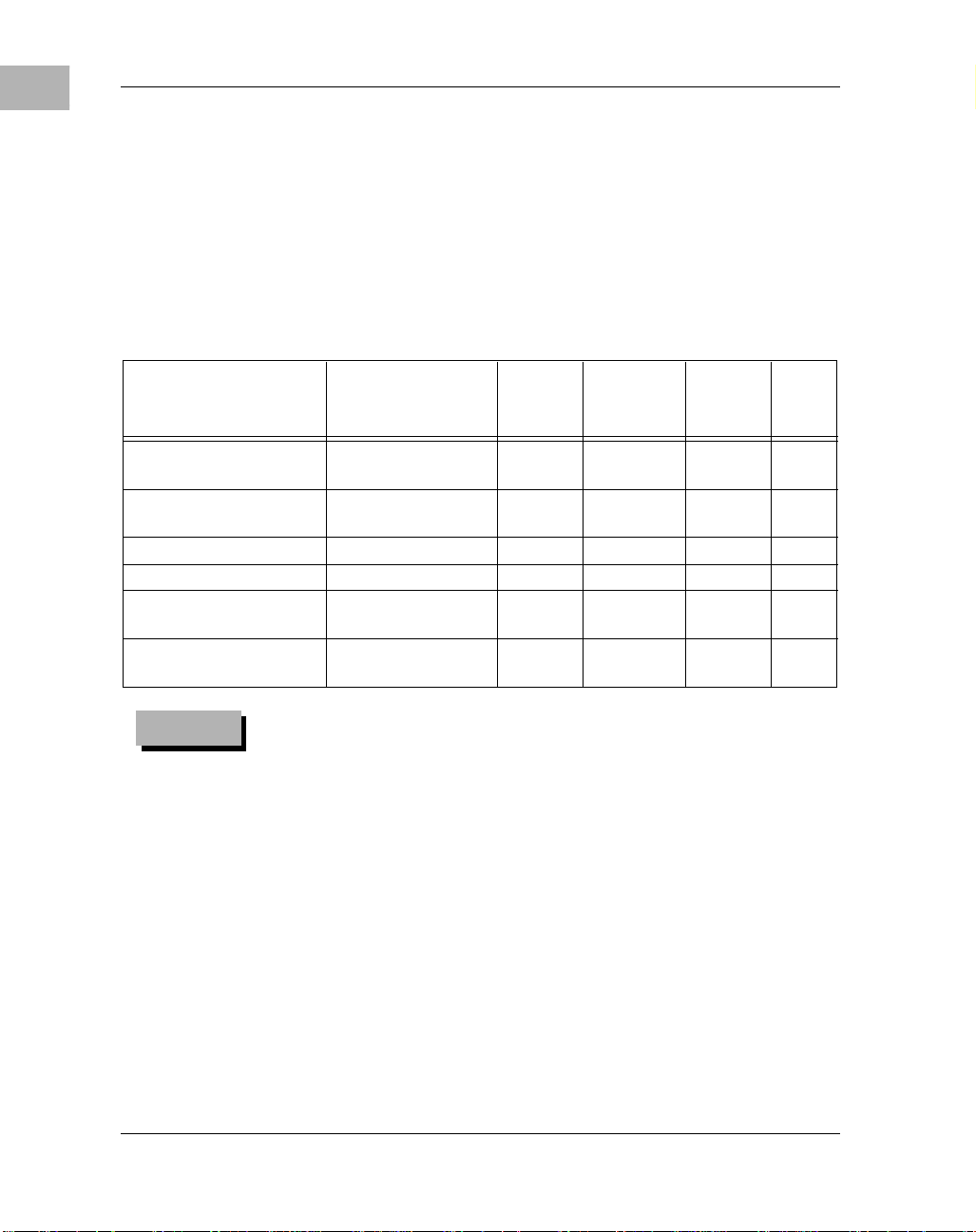
Specifications
The specifications for the MVME197LE are listed in Table 1-1.
Table 1-1. MVME197LE Specifications
Characteristics Specifications
Power requirements
Operating temperature
Storage temperature
Relative humidity
Physical dimensions:
PC board
Height
Width
Thickness
PC board with connectors
and front panel
Height
Width
Thickness
Board connectors:
P1 connector
P2 connector
J1 connector
J2 connector
+5 Vdc (+/- 2.5%), 4 A (typical), 5 A (maximum)
+12 Vdc (+/- 2.5% ), 10 0 m A ( ma ximum)
-12 Vdc (+/- 2.5%), 100 mA (maximum)
0° to 55° C at point of entry of forced air
(approximately 490 LFM)
-40° to 85° C
5% to 90% (non-condensing)
Double-high VMEboard
9.187 inches (233.35 mm)
6.299 inches (160.00 mm)
0.063 inch (1.60 mm )
10.309 inches (261.85 mm)
7.4 inches (188.00 mm)
0.80 inch (20.32 mm)
96-pin connector which provides the interface to the
VMEbus signals.
96-pin connector which provides the interface to the
extended VMEbus signals and other I/O signals.
20-pin connector which provides the interface to the remote
reset, abort, the LEDs, and three general purpose I/O
signals.
249-pin connector which provides the interface to the
MC88110 address, data, and control signals to and from the
mezzanine expansion.
Block Diagram
Figure 1-1 is a general block diagram of the MVME197LE.
1-4 Installation Guide
Page 21

Block Diagram
1
MVME197LEIG/D1 1-5
Page 22
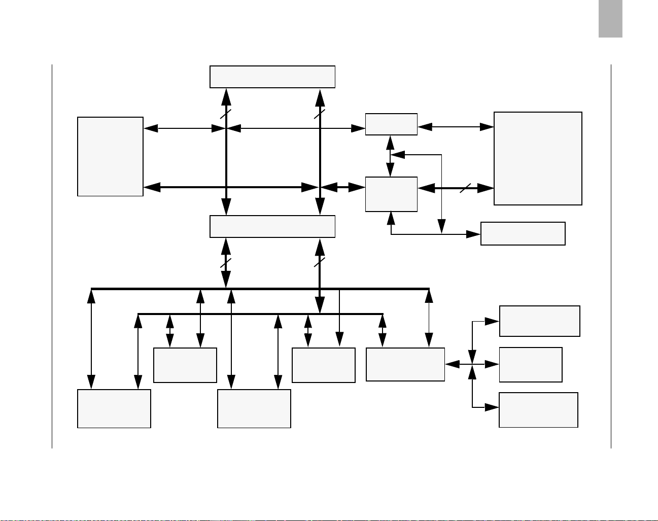
1
1-6 Installation Guide
Mezzanine
Port
Address Bus
Address 32
Address Bus
Data Bus
Address 32
Data Bus
MC88110
Data 64
PROCESSOR
BUS
BusSwitch
Data 32
MUX Address
DCAM
ECDM
(X4)
I2CBus
RAS, CAS
Data
Bus
256
LOCAL PERIPHERAL
BUS
Board Level Hardware Description
Memory Array
32/64 MB
I2C EEPROM
NVRAM/RTC
VMEbus
(VMEchip2)
LAN
82596CA
Flash
Memory
SCSI -II
NCR53710
Figure 1-1. MVME197LE Block Diagram
PCCchip2
BOOT
ROM
4 Serial Ports
CL-CD2401
Page 23

Functional Description
The following sections contain a functional description of the major blocks on
the MVME197LE single board computer.
Front Panel Switches and Indicators
There are two push-button switches and six LEDs on the front panel of the
MVME197LE module. The switches are RESET and ABORT. The RESET
switch (S3) will reset all onboard devices and drive the SYSRESET* signal if the
board is the system controller. The RESET switch (S3) will reset all onboard
devices except the DCAM and ECDM if the board is not th e system controller.
The VMEchip2 generates the SYSREST* signal. The BusSwitch combines the
local reset and the reset switch to generate a loca l board reset. Refer to the Reset
Driver section in the VMEchip2 chapter of the MVME197L E, MVME197DP, and
MVME197SP Singl e Board Computers Programmer’s Refer ence Guide for more
information.
When enabled by software, the ABORT switch (S2) generates an interrupt at a
user-programmable level. It is normally used to abort program execution and
return to the debugger. Refer to the VMEchip2 chapter of the MVME197LE,
MVME197DP, and MVME197S P Single Board Computer s Programmer’s Refe rence
Guide for more information.
Functional Description
1
The six LEDs on the MVME197LE front panel are: FAIL, SCON, RUN, LAN,
VME, and SCSI.
1. The yellow FAIL LED (DS1) is lit when the BRDFAIL signal line is active.
2. The green SCON LED (DS2) is lit when the VMEchip2 is the VMEbus
system controller.
3. The green RUN LED (DS3) is lit when the MC88110 bus MC* pin is low.
4. The green LAN LED (DS4) lights when the LAN chip is the local
peripheral bus master.
5. The green VME LED (DS5) lights when the board is using the VMEbus or
when the board is accessed by the VMEbus.
6. The green SCSI LED (DS6) lights when the SCSI chip is the local peripheral
bus master.
MVME197LEIG/D1 1-7
Page 24

1
Board Level Hardware Description
Data Bus Structure
The data bus structure is arranged to accommodate the various 8-bit, 16-bit,
32-bit, and 64-bit devices that reside on the module. Refer to the MVME197LE,
MVME197DP, and MVME197S P Single Board Computer s Programmer’s Refe rence
Guide and to the user’s guide for each device to determine its port size, data
bus connection, and any restrictions that apply when accessing the device.
MC88110 MPU
The MVME197LE is based on the MC88000 family and uses one MC88110
microprocessor unit. Refer to the MC88110 Second Generation RISC
Microprocessor User’s Manual for more information.
BOOT ROM
A socket for a 32-pin PLCC/CLCC ROM/EPROM referred to as BOOT ROM
or DROM (Download ROM) is provided. It is organized as a 128K x 8 device,
but as viewed from the processor it looks like a 16K x 64 memory. This
memory is mapped starting at location $FFF80000, but after a local reset it is
also mapped at location 0, providing a reset vector and bootstrap code for the
processor. The DR0 bit in the General Control Register (GCR) of the PCCchip2
must be cleared to disable the BOOT ROM memory map at 0.
Flash Memory
Up to 1MB of flash memory is available on the board. Flash memory works like
EPROM, but can be erased and reprogrammed by software. It is organized as
32 bits wide, but to the processor it looks as 64 bits wide. It is mapped at
location $FF800000. Reads can be of any size, including burst transfers, but
writes are always 32 bits wide, regardless of the size specified for the transfer.
For this reason, software should only use 32-bit write transfers. This memory
is controlled by the BusSwitch, and the memory size, access time, and write
enable capability can be programmed via the ROM Control Register (ROMCR)
in the BusSwitch. The flash memory can be accessed from the processor bus
only. It is not accessible from the local peripheral bus or VMEbus.
Onboard DRAM
The MVME197LE onboard DRAM (2 banks of 32MB memory, one optionally
installed) is sized at 32MB using 1M x 4 devices and configured as 256 bits
wide. The DRAM is four-way interleaved to efficiently support cache burst
cycles. The DRAM is controlled by the DCAM and ECDM, and the map
decoders in the DCAM can be programmed through the I2Cbus interface in
the ECDM to accommodate different base address(es) and sizes. The on board
1-8 Installation Guide
Page 25

DRAM is not disabled by a local peripheral bus reset. Refer to the DCAM and
ECDM chapters in the MVME197LE, MVME197DP, and MVME197SP Single
Board Computers Programmer’s Reference Guide for detailed programming
information.
Battery Backup RAM and Clock
The MK48T08 RAM and clock chip is used on the MVME197LE. This chip
provides a time of day clock, oscillator, crystal, power fail detection, memory
write protection, 8KB of RAM, an d a battery in one 28-pin package. The clock
provides seconds, minutes, hours, day, date, month, and year in BCD 24-hour
format. Corrections for 28-, 29-, (leap year) and 30-day months are
automatically made. No interrupts are generated by the clock. The MK48T08
is an 8-bit device; however the interface provided by the PCCchip2 supports
8-, 16-, and 32-bit accesses to the MK48T08. Refer to the PCCchip2 chapter in
the MVME197LE, MVME197DP, and MVME197SP Single Board Computers
Programmer’s Reference Guide and to the MK48T08 data sheet for detailed
programming information.
VMEbus Inte rface
The local peripheral bus to VMEbus interface, the VMEbus to local peripheral
bus interface, and the local-VMEbus DMA controller functions on the
MVME197LE are provided by the VMEchip2. The VMEchip2 can also provide
the VMEbus system controller functions. Refer to the VMEchip2 chapter in the
MVME197LE, MVME197DP, and MVME197SP Single Board Computers
Programmer’s Reference Guide for detailed programming information.
Functional Description
1
I/O Interfaces
The MVME197LE provides onboard I/O for many system applications. The
I/O functions include serial ports, a printer port, an Ethernet transceiver
interface, and a SCSI mass storage interface.
Serial Port Interface
The CD2401 serial controller chip (SCC) is used to implement the four serial
ports. The serial ports support the standard baud rates (110 to 38.4K baud).
Serial port 4 also supports synchronous modes of operation.
The four serial ports are different functionally because of the limited number
of pins on the I/O connector. Serial port 1 is a minimum function
asynchronous port. It uses RXD, CTS, TXD, and RTS. Serial ports 2 and 3 are
full function asynchronous ports. They use RXD, CTS, DCD, TXD, RTS, and
DTR. Serial port 4 is a full function asynchronous or synchronous port. It can
MVME197LEIG/D1 1-9
Page 26

1
Board Level Hardware Description
operate at synchronous bit rates up to 64k bits per second. It uses RXD, CTS,
DCD, RTS, and DTR. It also interfaces to the synchronous clock signal lines.
Refer to the MVME197LE, MVME197DP, and MVME197SP Single Board
Computers Prog rammer’s Refe rence Guide for drawings of the se rial port interface
connections.
All four serial ports use EIA-232-D drivers and receivers located on the main
board, and all the signal lines are routed to the I/O connector. The
configuration headers are located on the MVME712X transition board. An
external I/O transition board such as the MVME712X should be used to
convert the I/O connector pinout to industry-standard connectors.
The interface provided by the PCCchip2 allows the 16-bit CD2401 to appear at
contiguous addresses; however, accesses to the CD2401 must be 8 or 16 bits.
32-bit accesses are not permitted. Refer to the CD2401 data sheet and to the
PCCchip2 chapter in the MVME197L E, MV ME197DP, and MV ME197S P Sing le
Board Computers Programmer’s Reference Guide for detailed programming
information.
The CD2401 supports DMA operations to local memory. Because the CD2401
does not support a retry operation necessary to break VMEbus lo ck conditions,
the CD2401 DMA controllers should not be programmed to access the
VMEbus. The hardware does not restrict the CD2401 to onboard DRAM.
Printer Interface
The MVME197LE has a Centronics-compatible printer interface. The printer
interface is provided by the PCCchip2. Refer to the PCCchip2 chapter in the
MVME197LE, MVME197DP, and MVME197SP Single Board Computers
Programmer’s Reference Guide for detailed programming information and for
drawings of the printer port interface connections.
Ethernet Interface
The 82596CA is used to implement the Ethernet transceiver interface. The
82596CA accesses local RAM using DMA operations to perform its norm al
functions. Because the 82596CA has small internal buffers and the VMEbus
has an undefined latency period, buffer overrun may occur if the DMA is
programmed to access the VMEbus. Therefore, the 82596CA should not be
programmed to access the VMEbus.
Every MVME197LE module is assigned an Ethernet Station Address. This
address is $08003E2XXXXX, where XXXXX is the unique 5-nibble number
assigned to the board (i.e., every MVME197LE has a different value for
XXXXX).
1-10 Installation Guide
Page 27

The Ethernet Station Address is displayed on a label attached to the VMEbus
P2 connector. In addition, the eight bytes including the Ethernet address are
stored in the configuration area of the BBRAM, with the two lower bytes of
those set to 0. That is, 08003E2XXXXX0000 is stored in the BBRAM. At an
address of $FFFC1F2C, the upper four bytes (08003E2X) can be read. At an
address of $FFFC1F30, the lower four bytes (XXXX0000) can be read. Refer to
the BBRAM, TOD Clock memory map description later in this chapter. The
MVME197LE debugger has the capability to retrieve or set the Ethernet
address.
If the data in the BBRAM is lost, the user should use the number on the
VMEbus P2 connector label to restore it. Refer to the MVME197BUG 197Bug
Debugging Package User’s Manual.
The Ethernet transceiver interface is located on the MVME197LE main
module, and the industry standard connector is located on the MVME712X
transition module.
Support functions for the 82596CA are provided by the PCCchip2. Refer to the
82596CA LAN Coprocessor User’s Manual and to the PCCchip2 chapter in the
MVME197LE, MVME197DP, and MVME197SP Single Board Computers
Programmer’s Reference Guide for detailed programming information.
SCSI Interface
Functional Description
1
The MVME197LE provides for mass storage subsystems through the industrystandard SCSI bus. These subsystems may include hard and floppy disk
drives, streaming tape drives, and other mass storage devices. The SCSI
interface is implemented using the NCR 53C710 SCSI I/O controller.
Support functions for the 53C710 are provided by the PCCchip2. Refer to the
NCR 53C710 SCSI I/O Processor Data Manual and to the PCCchip2 chapter in the
MVME197LE, MVME197DP, and MVME197SP Single Board Computers
Programmer’s Reference Guide for detailed programming information.
SCSI Termination
The system configurer must ensure that the SCSI bus is terminated properly.
On the MVME197LE, the terminators are located on the P2 transition board.
The +5V power to the SCSI bus termination resistors is provided by the P2
transition board.
MVME197LEIG/D1 1-11
Page 28

1
Board Level Hardware Description
Peripheral Resources
The MVME197LE includes many resources for the local processor. These
include tick timers, software programmable hardware interrupts, watchdog
timer, and local peripheral bus timeout.
Programmable Tick Timers
Six 32-bit programmable tick timers with 1 µsec resolution are provided, two
in the BusSwitch, two in the VMEchip2, and two in the PCCchip2. The tick
timers can be programmed to generate periodic interrupts to the processor.
Refer to the VMEchip2, PCCchip2, and BusSwitch chapters in the MVM E197LE,
MVME197DP, and MVME197S P Single Board Computer s Programmer’s Refe rence
Guide for detailed programming information.
Watchdog Timer
A watchdog timer function is provided in the VMEchip2. When the watchdog
timer is enabled, it must be reset by software within the programmed time or
it times out. The watchdog can be programmed to generate a SYSRESET*
signal, local reset signal, or board fail if it times out. Refer to the VMEchip2
chapter in the MVME197LE, MVME197DP, and MVME197SP Single Board
Computers Programmer ’s Reference Guide for detailed programming
information.
Software-Programmable Hardware Interrupts
Eight software-programmable hardware interrupts are provided by the
VMEchip2. These interrupts allow software to create a hardware interrupt.
Refer to the VMEchip2 chapter in the MVME197LE, MVME197DP, and
MVME197SP Single Board Computers Programmer’s Reference Guide for detailed
programming information.
Processor Bus Timeout
The BusSwitch provides a bus timeout circuit for the processor bus. When
enabled by the BTIMER register in the BusSwitch, the timer starts counting
when DBB* is asserted, and if the cycle is not terminated (TA*, TEA*, or
TRTRY* asserted) before the programmed timeout period, TEA* is asserted.
This timer is disabled if the access goes to the local peripheral bus.
Local Peripheral Bus Timeout
The MVME197LE provides a timeout function for th e processor bus (MC88110
bus) and for the local peripheral bus (MC68040 compatible bus). When the
timer is enabled and a bus access times out, a Transfer Error Acknowledge
(TEA) signal is generated. The timeout value is selectable by software for 8
1-12 Installation Guide
Page 29

µsec, 64 µsec, 256 µs ec, or infinite for the local peripheral bus. The local
peripheral bus timer does not operate during VMEbus bound cycles. VMEbus
bound cycles are timed by the VMEbus access timer and the VMEbus global
timer.
Interrupt Sources
MVME197LE MPU interrupts are channeled through the BusSwitch. They
may come from internal BusSwitch sources as well as from the PCCchip2 (IPL
inputs to the BusSwitch), the VMEchip2 (XIPL inputs to the BusSwitch), and
other external sources (PALINT and IRQ). The BusSwitch may also generate
the non-maskable interrupt (NMI) signal to the MPU from the ABORT pushbutton switch. Refer to the BusSwitch, PCCchip2, and VMEchip2 chapters in the
MVME197LE, MVME197DP, and MVME197SP Single Board Computers
Programmer’s Reference Guide for more detailed information.
Connectors
The MVME197LE has two 64-position DIN connectors: P1 and P2. Connector
P1 rows A, B, C, and connector P2 row B pro vide the VMEbus interconnection.
Connector P2 rows A and C provide the interconnect to the SCSI bus, the serial
ports, the Ethernet interface, and the Centronics printer. There is a 249-pin
mezzanine connector (J2) with the MC88110 bus interface. This mezzanine
connector is for other MVME197 module expansion. On the MVME197LE
there is also a 20-pin general purpose connector (J1) which provides the
interconnect to the LEDs and the reset and abort signals. This connector is
different for the other modules in the MVME197 series. Refer to the board
specific SIMVME197 Single Board Com puter Support Information manual for
detailed connector signal descriptions.
Memory Maps
1
Memory Maps
There are three points of view for the memory maps: 1) the mapping of all
resources as viewed by the Processor Bus (MC88110 bus), 2) the mapping of
onboard/off-board resources as viewed from the Local Peripheral Bus
(MC68040 compatible bus), and 3) the mapping of onboard resources as
viewed by VMEbus Masters (VMEbus memory map).
Processor Bus Memory Map
Care should be taken, since all three maps are programmable. It is
recommended that direct mapping from the Processor Bus to the Local
Peripheral Bus be used.
MVME197LEIG/D1 1-13
Page 30
1
Board Level Hardware Description
The memory maps of MVME197LE devices are provided in the following
tables. Table 1-2 is the entire map from $00000000 to $FFFFFFFF. Many areas
of the map are user-programmable, and suggested uses are shown in the table.
This is assuming no address translation is used between the processor and
local peripheral bus and between the local peripheral bus and VMEbus. The
cache inhibit function is programmable in the MC88110. The onboard I/O
space must be marked cache inhibit and serialized in its page table. Table 1-3
further defines the map for the local devices.
Table 1-2. Processor Bus Memory Map
Address Devices Port Size Software Notes
Range Accessed Size Cache
Inhibit
$00000000 - DRAM S IZE User Programmable D64 DRAMSIZE N 1
(Onboard DRAM)
DRAMSIZE - $FF7FFFFF User Programmable D32/D16 3GB ? 2,3
(VMEbus)
$FF800000 - $FFBFFFFF Flash Memory D32 4MB N 5
$FFC00000 - $FFEFFFFF reserved --- 3MB --- 4
$FFF00000 - $FFFEFFFF Local Devices D32-D8 1MB Y
(Refer to next table)
$FFFF0000 - $FFFFFFFF User Programmable D32/D16 64KB ? 1,3
(VMEbus A16)
Notes
1-14 Installation Guide
1. This area is user-programmable. The suggested use is
shown in the table. The DRAM decoder i s programmed
in the DCAM through the ECDM I2CBus interface. The
Processor Bus to Local Peripheral Bus and the Local
Peripheral Bus to Processor Bus decoders are
programmed in the BusSwitch. The Local Peripheral to
VMEbus (master) and VMEbus to Local Peripheral Bus
(slave) decoders are programmed in the VMEchip2.
2. Size is approximate.
3. Cache inhibit depends on devices in area mapped.
4. This area is not decoded. If these locations are accessed
and the local peripheral bus timer is enabled, the cycle
times out and is terminated by a TEA signal.
5. This area is user programmable via the BusSwitch.
Default size is 4 megabytes.
Page 31

Memory Maps
The following table focuses on the Local Devices portion of the Memory Map.
Table 1-3. Local Devices Memory Map
Address Range Devices Accessed Port Size Size Notes
$FFF00000 - $FFF00FFF BusSwitch D64-D8 4KB 1
$FFF01000 - $FFF01FFF ECDM (DCAM access) --- 4KB 1
$FFF02000 - $FFF02FFF reserved --- 4KB 4
$FFF03000 - $FFF03FFF reserved --- 4KB 4
$FFF04000 - $FFF04FFF reserved --- 4KB 4
$FFF05000 - $FFF05FFF reserved --- 4KB 4
$FFF06000 - $FFF06FFF reserved --- 4KB 4
$FFF07000 - $FFF07FFF User defined --- 4KB 4
$FFF08000 - $FFF3FFFF reserved --- 224KB 4
$FFF40000 - $FFF400FF VMEchip2 (LCSR) D32 256B 1,2,3
$FFF40100 - $FFF401FF VMEchip2 (GCSR) D32-D8 256B 1,2,3
$FFF40200 - $FFF40FFF reserved --- 3.5KB 4,5
$FFF41000 - $FFF41FFF reserved --- 4KB 4
$FFF42000 - $FFF42FFF PCCchip2 D32-D8 4KB 1,2
$FFF43000 - $FFF43FFF reserved --- 4KB 4
$FFF44000 - $FFF44FFF reserved --- 4KB 3
$FFF45000 - $FFF45FFF CD2401 (Serial Comm. Cont.) D16-D8 4KB 1,2
$FFF46000 - $FFF46FFF 82596CA (LAN) D32 4KB 1,2,6
$FFF47000 - $FFF47FFF 53C710 (SCSI) D32/D8 4KB 1,2
$FFF48000 - $FFF4FFFF reserved --- 32KB 4
$FFF50000 - $FFF6FFFF reserved --- 128KB 4
$FFF70000 - $FFF77FFF reserved --- 32KB 4
$FFF78000 - $FFF7FFFF reserved --- 288KB 4
$FFF80000 - $FFFBFFFF DROM (BOOT ROM) --- 256KB 7
$FFFC0000 - $FFFCFFFF MK48T08 (BBRAM,TOD Clk) D32-D8 64KB 1,2
$FFFD0000- $FFFEFFFF reserved --- 128KB 4
1
Notes
1. For a complete description of the register bits, refer to
the appropriate data sheet for the specific chip. For a
more detailed memory map refer to the detailed
peripheral device memory maps in the MVME197LE,
MVME197DP, and MVME197SP Single Board
Computers Programmer’s Reference Guide.
2. Address is the physical address going to the device. It is
after the BusSwitch translation from the MC88110
address to the device seen address.
MVME197LEIG/D1 1-15
Page 32

1
Board Level Hardware Description
3. Writes to the LCSR in the VM Echip2 must be 32 bits.
LCSR writes of 8 o r 16 bits terminate with a TEA signal.
Writes to the GCSR may be 8, 16, or 32 bits. Reads t o the
LCSR and GCSR may be 8, 16, or 32 bits.
4. This area does not return an acknowledge signal. If the
processor bus timeout timer is enabled, the access times
out and is terminated by a TEA signal.
5. Size is approximate.
6. Port commands to the 82596CA must be written as two
16-bit writes: upper word first and lower word second.
7. DROM (BOOT ROM) appears at $0 following a local
peripheral bus reset. Th e D RO M appears at 0 until the
DR0 bit is cleared in the PCCchip2. The DR0 bit is
located at address 0 bit D15. The DROM must be
disabled at 0 before the DRAM is accessed.
VMEbus Memory Map
This section describes the mapping of local resources as viewed by VMEbus
masters.
VMEbus Accesses to the Local Peripheral Bus
The VMEchip2 includes a user-programmable map decoder for the VMEbus
to local peripheral bus interface. The map decoder allows the user to program
the starting and ending address and the modifiers the MVME197LE responds
to.
VMEbus Short I/O Memory Map
The VMEchip2 includes a user-programmable map decoder for the GCSR
(Global Control and Status Registers). The GCSR map decoder allows the user
to program the starting address of the GCSR in the VMEbus short I/O space.
1-16 Installation Guide
Page 33

HARDWARE PREPARATION
Introduction
This chapter provides unpacking instructions, hardware preparation, and
installation instructions for the MVME197LE VMEmodule. The MVME712X
transition module hardware preparation is provided in separate manuals,
refer to the Related Documentation section of this guide.
Unpacking Instructions
Note
Carefully unpack the equipment from the shipping carton. Refer to the
packing list and verify that all items are present. Save the shipping carton and
packing materials for storing or reshipping of the equipment.
Caution
If shipping carton is damaged upon receipt, request that the
carrier’s agent be present during unpacking and inspection
of equipment.
Avoid touching areas of integrated circuit s. Sta tic discha rge
can damage these components.
AND INSTALLATION
2
Inspect the equipment for any shipping damage. If no damage exists, then the
module can be prepared for operation according to the following sections of
this chapter.
Hardware Preparation
To select the desired configuration and ensure proper operation of the
MVME197LE module, certain modifications may be necessary before
installation. These modifications are made through switch settings as
described in the following sections. Many other modifications are done by
setting bits in control registers after the MVME 197LE has been installed in a
system. (The MVME197LE registers are described in the MVME197LE,
MVME197DP, and MVME197SP S ingle Board Computers Programm er’s Reference
Guide as listed in the Related Documentation section of this guide).
MVME197LEIG/D12-1
Page 34

Hardware Preparation and Installation
2
2-2 Installation Guide
Page 35

MVME197LEIG/D1 2-3
VMEbus CONNECTOR P1
VMEbus CONNECTOR P2
P1 P2
A1
B1
C1
A32
B32
C32
A1
B1
C1
1A17
1A1
1A1
2A17
3A1
A32
B32
C32
3A17
1E1
1E17
1E1
MEZZANINE CONNECTOR J2
S6
S1
12345678
O
N
CONFIGURATION SWITCH S1
GENERAL PURPOSE/SCON
MODULE CONNECTOR J1
REMOTE RESET/ABORT/LEDS
20
9
2
J1
DS2
SCON
1
DS3
RUN
19
DS1
FAIL
DS4
LAN
ABORT
RESET
SWITCH
SWITCH
S2
DS6
DS5
SCSI
VME
S3
S2 S3
CONFIGURATION SWITCH S6
SERIAL PORT 4 CLOCK SELECT
MVME197LE
Figure 2-1. MVME197LE Switches, Connectors, and LED Indicators Location Diagram
O
N
2E17
12
3E1
3E17
Hardware Preparation
2
Page 36

Hardware Preparation and Installation
2
Configuration Switches
The location of the switches, connectors, and LED indicators on the
MVME197LE is illustrated in Figure 2-1. The MVME197LE has been factory
tested and is shipped with factory switch settings that are described in the
following sections. The MVME197LE operates with its required and factoryinstalled Debug Monitor, MVME197Bug (197Bug), with these factory switch
setting.
Configuration Switch S1: General Information
Switch S1 is a bank of nine two-way switch segments. The following
illustration shows the factory configuration of switch S1. The bit values are
read as a one when the switch is OFF (open), and as a zero when the switch is
ON (closed). The default value for switch S1 is shown below.
Switch S1
1
O
N
2 3 4 5 6 7 8 9
CLOSED
OPEN
System Controller (SCON)
General Purpose Input 7 (GPI7)
General Purpose Input 6 (GPI6)
General Purpose Input 5 (GPI5)
General Purpose Input 4 (GPI4)
General Purpose Input 3 (GPI3)
General Purpose Input 2 (GPI2)
General Purpose Input 1 (GPI1)
General Purpose Input 0 (GPI0)
(FACTORY CONFIGURATION)
2-4 Installation Guide
Page 37

Hardware Preparation
Configuration Switch S1: General Purpose Functions (S1-1 to S1-8)
The eight General Purpose Input lines (GPI0-GPI7) on the MVME197LE may
be configured with selectable switch segments S1-1 through S1-8. These
switches can be read as a register (at $FFF40088) in the VMEchip2 LCSR. Refer
to the VMEchip2 chapter in the MVME197LE, MVME197DP, an d MVME197SP
Single Board Computers Programmer’s Reference Guide for the status of lines GPI0
through GPI7. Factory configuration is with the general purposes input lines
disabled (open).
Switch S1
1
O
O
N
N
S1-1 to S1-8: OFF -- All Ones (FACTORY CON FIGU RATION )
Configuration Switch S1: System Controller Enable Function (S1-9)
The MVME197LE can be the system controller. The system controller
function is enabled or disabled by configuring selectable switch segment
S1-9. When the MVME197LE is the system controller, the SCON LED is
turned ON. T he VMEchi p2 may b e configu red as a system controller as
illustrated below. Factory configuration is with the system controller
switch enabled (closed).
2 3 4 5 6 7 8 9
CLOSED
OPEN
2
Switch S1
O
O
N
N
S1-9: ON -- MVME197 IS the System Controller
(FACTORY CONF IG URAT ION )
91 2 3 4 5 6 7 8
CLOSED
OPEN
Switch S1
O
N
S1-9: OFF -- MVME197 IS NOT the System Controller
MVME197LEIG/D1 2-5
91 2 3 4 5 6 7 8
CLOSED
OPEN
Page 38

Hardware Preparation and Installation
2
Configuration Switch S6: Serial Port 4 Clock Select (S6-1, S6-2)
Serial port 4 can be configured to use clock signals provided by the RTXC4 and
TRXC4 signal lines. Switch segments S6-1 and S6-2 on the MVME197LE
configures serial port 4 to drive or receive TRXC4 and RTXC4, respectively.
Factory configuration is with serial port 4 set to receive both signals (open).
The remaining configuration of the clock lines is accomplished by using the
Serial Port 4 Clock Configuration Select header on the MVME712M transition
module. Refer to the MVME712M Transition Module and P2 Adapter Board
User’s Manual for configuration of that header.
Switch S6
1 2
O
N
Receive TRXC4 Receive RTXC4
(FACTORY CONFIGURATION)
Switch S6
1 2
O
N
CLOSED
OPEN
CLOSED
OPEN
Drive TRXC4 Drive RTXCC4
Installation Instructions
The following sections discuss i nsta llation of the MVME197LE into a VME
chassis, and system considerations. Ensure that BOOT ROM device is
installed. Ensure that all switches are configured as desired.
2-6 Installation Guide
Page 39

Installation Instructions
MVME197LE Module Installation
Now that the MVME197LE module is ready for installation, proceed as
follows:
a. Turn all equipment power OFF and disconnect the power cable from the
power source.
Caution
!
WARNING
b. Remove the chassis cover as instructed in the equipment user’s manual.
c. Remove the filler panel(s) from the appropriate card slot(s) at the front and
Inserting or removing modules while power is applied
could result in damage to module components.
DANGEROUS VOLTAGES, CAPABLE OF CAUSING
DEATH, ARE PRESENT IN THIS EQUIPMENT. USE
EXTREME CAUTION WHEN HANDLING, TESTING,
AND ADJUSTING.
rear of the chassis (if the chassis has a rear card cage). The MVME197LE
module requires power from both P1 and P2. It may be installed in any
double-height unused card slot, if it is not configured as the system
controller. If the MVME197LE is configured as the system controller, it
must be installed in the left-most card slot (slot 1) to correctly initiate the
bus-grant daisy-chain and to have proper operation of the IACK-daisychain driver. The MVME197LE is to be installed in the front of the chassis
and the MVME712X trans ition board whi ch has a double- wide front panel
is to be installed in the rear of the chassis.
2
d. Carefully slide the MVME197LE module in to the card slot. Be sure the
module is seated properly into the P1 and P2 connectors on the backplane.
Do not damage or bend connector pins. Fasten the modu le in the chassis
with screws provided, making good contact with the transverse mounting
rails to minimize RFI emiss ions.
e. Remove the IACK and BG jumpers from the header on the chassis
backplane for the card slot in which the MVME197LE is installed.
f. Connect the P2 Adapter Board and specified cable(s) to the MVME197LE
at P2 on the backplane at the MVME197LE slot, to mate with (optional)
terminals or other peripherals at the EIA-232-D serial ports, parallel port,
SCSI ports, and LAN Ethernet port. Refer to the manuals listed in Related
Documentation section for information on installing the P2 Adapter Board
and the MVME712X transition module. (Some connection diagrams are
MVME197LEIG/D1 2-7
Page 40

Hardware Preparation and Installation
2
provided in the MVME197LE, MVME197DP, and MVME197SP Single
Board Computers Prog rammer’s Reference Guide). Some cable(s) are not
provided with the MVME712X module and therefore, are made or
provided by the user. (Motorola recommends using shielded cables for all
connections to peripherals to minimize radiation). Connect the
peripherals to the cable(s).
g. Install any other required VMEmodules in the system.
h. Replace the chassis cover.
i. Connect the power cable to the ac power source and turn the equipment
power ON.
System Considerations
The MVME197LE needs to draw power from both connectors P1 an d P2 of the
VMEbus backplane. Connector P2 is also used for the upper 16 bits of data for
32-bit transfers, and for the upper 8 address lines for the extend ed addr essing
mode. The MVME197LE may not operate properly without its main board
connected to connectors P1 and P2 of the VMEbus backplane.
Whether the MVME197LE operates as a VMEbus master or as a VMEbus slave,
it is configured for 32 bits of address and for 32 bits of data (A32/D32).
However, it handles A16 or A24 devices in ce rtain address ran ges. D8 an d/or
D16 devices in the system must be handled by software. Refer to the memory
maps in the MVME197LE, MVME197DP, and MVME197SP Single Board
Computers Programmer ’s Reference Guide.
The MVME197LE contains shared onboard DRAM whose base address is
software-selectable. Both the onboard processor and off-board VMEbus
devices see this local DRAM at base physical address $00000000, as
programmed by the MVME197Bug firmware. This may be changed, by
software, to any other base address. Refer to the MVME197LE, MVME197DP,
and MVME197SP Single Board Computers Programmer’s Reference Guide for
details.
If the MVME197LE tries to access off-board resources in a non-existent
location, and is not the system controller, and if the system does not have a
global bus timeout, the MVME197LE waits forever for the VMEbus cycle to
complete. This would cause the system to hang up. There is only one situation
in which the system might lack this global bus timeout: when the
MVME197LE is not the system controller and there is no global bus timeout
elsewhere in the system.
2-8 Installation Guide
Page 41

Installation Instructions
Multiple MVME197LE modules may be configured into a single VME card
cage. In general, hardware multiprocessor features are supported.
Other MPUs on the VMEbus can interrupt, disable, communicate with and
determine the operational status of the RISC processor(s). One register of the
GCSR set includes four bits which function as location monitors to allow one
MVME197LE processor to broadcast a signal to other MVME197LE
processors, if any. All eight registers are accessible from any local processor as
well as from the VMEbus.
The MVME197LE provides +12 Vdc power to the Ethernet LAN transceiver
interface through a 1 amp fuse (F2) located on the MVME197LE module. If the
Ethernet transceiver fails to operate, check the fuse. When using the
MVME712M transition module, the yellow LED (DS1) on the MVME712M
front panel lights when LAN power is available, indicating that the fuse is
good.
2
MVME197LEIG/D1 2-9
Page 42

Hardware Preparation and Installation
2
2-10 Installation Guide
Page 43

DEBUGGER GENERAL
Overview of M88000 Firmware
The firmware for the M88000-based (88K) series of board and system level
products has a common genealogy, deriving from the BUG firmware currently
used on all Motorola M68000-based (68K) CPU modules. The M88000
firmware family provides a high degree of functionality and user friendliness,
and yet stresses portability and ease of maintenance. This member of the
M88000 firmware family is implemented on the MVME197LE Single Board
Computer, and is known as the MVME197BUG, or just 197Bug.
Description of 197Bug
The 197Bug package, MVME197BU G, is a powerful evaluation and debu gging
tool for systems built around the MVME197 series of RISC-based
microcomputers. Facilities are available for loading and executing user
programs under complete operator control for system evaluation. 197Bug
includes commands for display and modification of memory, breakpoint and
tracing capabilities, a powerful assembler/dis as sembler useful for patching
programs, and a self-test at power-up feature which verifies the integrity of the
system. Various 197Bug routines that handle I/O, data conversion, and string
functions are available to user programs through the TR AP #496 handler. Th e
TRAP #496 handler is accessible through any of the trap exception commands
TB0, TB1, TBND, and TCND, with trap vector #496.
INFORMATION
3
197Bug consists of three parts:
❏ A command-driven user-interactive software debugger, described in a
later chapter (Using the 197Bug De bugg er) and hereaf ter refe rred to as “the
debugger”.
❏ A command-driven diagnostic package for the MVME197LE hardware,
described in the MVME197BUG 197Bug Diagnostic Firmware User’s Manual
and hereafter referred to as “the diagnostics”.
❏ A user interface which accepts commands from the system console
terminal.
When using 197Bug, the user operates out o f either th e d ebugger directory or
the diagnostic directory. If the user is in the debugger directory, then the
debugger prompt “197-Bug>” is displayed and the user has all of the
debugger commands at his or her disposal. If in the diagnostic directory, then
MVME197LEIG/D13-1
Page 44

Debugger General Information
the diagnostic prompt “197-Diag>” is displayed and the user has all of the
diagnostic commands at his disposal as well as all of the debugger commands.
The user may switch between directories by using the Switch Directories (SD)
3
command, or may examine the commands in the particular directory that the
user is currently in by using the Help (HE) command.
Because 197Bug is command-driven, it performs its various operations in
response to user commands entered at the keyboard. When a command is
entered, 197Bug executes the command and th e pro mpt reappea rs. Ho wever,
if a command is entered which causes execution of user target code (e.g.,
“GO”), then control may or may not return to 197Bug, depending on the
outcome of the user program.
Comparison With M68000-Based Firmware
Those users who have used one or more of Motorola's other debugging
packages will find 197Bug very similar, after making due allowances for the
architectural differences between the M68000 and M88000 CPU arch itectures.
These are primarily reflected in the instruction mnemonics and addressing
modes of the assembler/disassembler, and in the use of registers instead of the
stack for the passing of arguments to or from the TRAP #496 handler. Some
effort has also been made to make the interactive commands more consistent.
For example, delimiters between commands and arguments may now be
commas or spaces interchangeably.
197Bug Implementation
MVME197BUG is written largely in the “C ” programming language,
providing benefits of portability and maintainab ility. Where necessary,
assembler has been used in the form of separately compiled modules
containing only assembler code - no mixed language modules are used.
Physically, 197Bug is contained in the onboard flash memory. The executable
code is checksummed at every power-on or reset firmware entry, and the
result (which includes a pre-calculated checksum contained in the flash
memory), is tested for an expected zero. Thus, users are cautioned against
modification of the flash memory unless re-checksum precautions are taken.
Installation and Start-up
Even though the MVME197Bug flash memory devices are installed on the
MVME197LE module, for 197Bug to operate properly with the MVME 197 LE,
follow this set-up procedure.
3-2 Installation Guide
Page 45

Installation and Start-up
Caution
1. Turn all equipment power OFF. Refer to the Hardware Preparation and
2. Refer to the set-up procedure for the user’ s particular chassis or system for
3. Connect the terminal which is to be used as the 197 Bug system consol e to
Inserting or removing modules while power is applied
could damage module components.
3
Installation chapter in this manual for selecting the configuration switch
settings required for the user’s particular application.
details concerning the installation of the MVME197LE.
the default debug EIA-232-D port at serial port 1 on backplane connector
P2 through an MVME712X transition module. Refer to the MVME197LE,
MVME197DP, and MVME197SP Single Board Computers Programmer’s
Reference Guide for some possible connection diagrams. Set up the terminal
as follows:
– eight bits per char acter
– one stop bit per character
– parity disabled (no parity)
– baud rate 9600 baud (default baud rate of the MVME197LE ports at
power-up)
After power-up, the baud rate of the debug port can be reconfigured by
using the Port Format (PF) command of the 197Bug debugger.
Note
4. If it is desired to connect devices (such as a host computer system and/or
MVME197LEIG/D1 3-3
In order for high-baud rat e serial comm unication betw een
197Bug and the terminal to work, the terminal must d o some
form of handshaking. If the terminal being used does not
do hardware handshaking via the CTS line, then it must do
XON/XOFF handshaking. If the user gets garbled messages
and missing characters, then the user should check the
terminal to make sure XON/XOFF handshaking is enabled.
a serial printer) to the other EIA-232-D port connectors (marked SERIAL
PORTS 2, 3, and 4 on the MVME712X transition module), connect the
appropriate cables and configure the port(s) as detailed in step 3 above.
After power-up, this(these) port(s) can be reconfigured by programming
the MVME197LE CD2401 Serial Controller Chip (SCC), or by using the
197Bug PF command.
Page 46

Debugger General Information
Note that the MVME197LE also contains a parallel port. To use a parallel
device, such as a printer , with the MVME197LE, con nect it to the “printer”
port at P2 through an MVME712X transition module. Refer to the
3
MVME197LE, MVME197DP, and MVME197SP Single Board Computers
Programmer’s Reference Guide for some possible connection diagrams.
However , you could a lso use a module such as the MVME335 for a parallel
port connection.
5. Power up the system. 197Bug executes some self-checks and displays the
debugger prompt “197-Bug>” (if 197Bug is in Board Mode). However, if
the ENV command has put 197Bug in System Mode, the system performs
a self test and tries to autoboot. Refer to the ENV and MENU commands.
They are listed in Table 4-1.
If the confidence test fails, the test is aborted when the first fault is
encountered. If possible, an appropriate message is displayed, and contr ol
then returns to the menu.
Autoboot
Autoboot is a software routine that is contained in the 197Bug to provide an
independent mechanism for booting an operating system. This autoboot
routine automatically scans for controllers and devices in a specified sequence
until a valid bootable device containing a boot media is f ound or the list is
exhausted. If a valid bootable device is found, a boot from that device is
started. The controller scanning sequence goes from the lowest controller
Logical Unit Number (LUN) detected to the highest LUN detected. (Refer to
Appendix B for default LUNs).
At power-up, Autoboot is enabled, and providing the drive and controller
numbers encountered are valid, the following message is displayed upon the
system console:
“Autoboot in progress... To abort hit <BREAK>”
Following this message there is approximately a thirty-second delay while the
debug firmware waits for the various controllers and drives to come up to
speed. Then the actual I/O is begun: the program pointed to within the
volume ID of the media specified is loaded into RAM and control passed to it.
If, however, during this time the user wants to gain control without Autoboot,
the <BREAK> key or the software ABORT or RESET switches can be pressed.
Autoboot is controlled by parameters contained in the ENV command. These
parameters allow the selection of specific boot devices and files, and allow
programming of the Boot delay. Refer to the ENV comman d in Appendix A for
more details.
3-4 Installation Guide
Page 47

ROMboot
Caution
ROMboot
This function is configured/enabled by the Envir onment (ENV) command and
executed at power-up (optionally also at reset) or by the RB command
assuming there is valid code in the flash memories (or optionally elsewhere on
the module or VMEbus) to support it. If ROMboot code is installed, a userwritten routine is given control (if the routine meets the format requirements).
One use of ROMboot might be resetting SYSFAIL* on an unintelligent
controller module. The NORB command disables the function.
For a user’s ROMb oot module to gain control through the ROMboot linkage,
four requirements must be met:
1. Power must have just been applied (but the ENV command can change
this to also respond to any reset).
2. The user’s r outine must be located within the MVME197LE ROM memory
map (but the ENV command can change this to any other portion of the
onboard memory, or even offboard VMEbus memory).
3. The ASCII string “BOOT” must be located within the specified memory
range.
4. The user's routine must pass a checksum test, which ensures that this
routine was really intended to receive control at power-up.
Although streaming tape can be used to autoboot, the same
power supply must be connected to the streaming tape
drive, controller, and the MVME197LE. At power-up, the
tape controller will position the streaming tape to load point
where the volume ID can correctly be read and used.
If, however, the MVME197LE loses power but the controlle r
does not, and the tape happens not to be at load point, the
sequences of commands required (attach and rewind)
cannot be given to the co ntroller and autoboot will not be
successful.
3
For complete details on how to use ROMboot, refer to the MVME197BUG
197Bug Debugging Package User’s Manual.
Network Boot
Network Auto Boot is a software routine contained in the 197Bug that
provides a mechanism for booting an operating system using a network (local
Ethernet interface) as the boot device. The Network Auto Boot routine
MVME197LEIG/D1 3-5
Page 48

Debugger General Information
automatically scans for controllers and devices in a specified sequence until a
valid bootable device containing a boot media is found or the list is exhausted.
If a valid bootable device is found, a boot from that device is started. The
3
controller scanning sequence goes from the lowest controller Logical Unit
Number (LUN) detected to the highest LUN detected. (Refer to Appendix C
for default LUNs).
At power-up, Network Boot is enabled, and providing the drive and controller
numbers encountered are valid, the following message is displayed upon the
system console:
“Network Boot in progress... To abort hit <BREAK>”
Following this message there is approximately a thirty-second delay while the
debug firmware waits for the various controllers and drives to come up to
speed. Then the actual I/O is begun: the program pointed to within the
volume ID of the media specified is loaded into RAM and control passed to it.
If, however, during this time you want to gain control without Network Boot,
you can press the <BREAK> key or the software ABOR T or RES E T switches.
Network Auto Boot is controlled by parameters contained in the NIOT and
ENV commands. These parameters allow the selection of specific boot devices,
systems, and files, and allow programming of the Boot delay. Refer to the ENV
command in Appendix A for more details.
Restarting the System
The user can initialize the system to a known state in three different ways:
reset, abort, and break. Each has characteristics which make it more
appropriate than the others in certain situations.
The debugger has a special feature upon a reset condition. This feature is
activated by depressing the RESET and ABORT switches at the same time.
This feature instructs the debugger to use the default setup/operation
parameters in ROM versus the user’ s setup/operation parameters in NVRAM.
This feature can be used in the event the user’s setup/operation parameters
are corrupted or do not meet a sanity check. Refer to the ENV command
(Appendix A) for the ROM defaults.
Reset
Pressing and releasing the MVME197LE front panel RESET sw itch initiates a
system reset. COLD and WARM reset modes are available and are selected by
using the RESET command. By default, 197Bug is in COLD mode. During
COLD reset, a total system initialization takes place, as if the MVME197LE had
3-6 Installation Guide
Page 49

Abort
Restarting the System
just been powered up. All static variables (including disk device and controller
parameters) are restored to their default states. The breakpoint table and offset
registers are cleared. The target registers are invalidated. Input and output
character queues are cleared. Onboard devices (timer, serial ports, etc.) are
reset, and the first two serial ports are reconfigured to their default state.
During WARM reset, the 197Bug variables and tables are preserved, as well as
the target state registers and breakpoints.
Reset must be used if the processor ever halts, or if the 197Bug environment is
ever lost (vector table is destroyed, stack corrupted, etc.).
Abort is invoked by pressing and releasing the ABORT swi tch on the
MVME197LE front panel. Whenever abort is invoked when executing a user
program (running target code), a “snapshot” of the processor state is captured
and stored in the target registers. (When working in the debugger, abort
captures and stores only the Instruction Pointer (IP), status register, and
format/vector information). For this reason, abort is most appropriate when
terminating a user program that is being debugged. Abort should be used to
regain control if the program gets caught in a loop, etc. The target IP, register
contents, etc., help to pinpoint the malfunction.
3
Pressing and releasing the ABORT switch generates a lo cal board condition
which may interrupt the processor if enabled. The target registers, reflecting
the machine state at the time the ABORT switch was pressed, are displayed on
the screen. Any breakpoints installed in the user code are removed and the
breakpoint table remains intact. Control is returned to the debugger.
Break
A “Break” is generated by pressing and releasing the BREAK key on the
terminal keyboard. Break does not generate an interrupt. The only time break
is recognized is when characters are sent or received by the console port. Break
removes any breakpoints in the user code and keeps the breakpoint table
intact. Break also takes a snapshot of the machine state if the function was
entered using SYSCALL. This machine state is then accessible to the user for
diagnostic purposes.
Many times it is desired to terminate a debugger command prior to its
completion, for example, the display of a large block of memory. Break a llows
the user to terminate the command.
MVME197LEIG/D1 3-7
Page 50

Debugger General Information
SYSFAIL* Assertion/Negation
Upon a reset/power up condition the debugger asserts the VMEbus SYSFAIL*
line (refer to the VMEbus specification). SYSFAIL* stays asserted if any of the
3
following has occurred:
❏ confidence test failure
❏ NVRAM checksum error
❏ NVRAM low battery condition
❏ local memory configuration status
❏ self test (if system mode) has completed with error
❏ MPU clock speed calculation failure
After debugger initialization is done and any of the above situations has not
occurred, the SYSFAIL* line is negated. This indicates to the user or VMEbus
masters the state of the debugger. In a multi-computer configuration, other
VMEbus masters could view the pertinent control and status registers to
determine which CPU is asserting SYSFAIL*. SYSFAIL* assertion/negation is
also affected by the ENV command. Refer to Appendix A.
MPU Clock Speed Calculation
The clock speed of the microprocessor is calculated and checked against a user
definable parameter housed in NVRAM (refer to the ENV command). If the
check fails, a warning message is displayed. The calculated clock speed is also
checked against known clock speeds and tolerances.
Memory Requirements
The program portion of 197Bug is approximately 1 megabyte of code,
consisting of download, debugger, and diagnostic packages and contained
entirely in the flash memory. The flash memory on the MVME197LE is
mapped starting at location $FF800000.
197Bug requires a minimum of 64KB of contiguous read/write memory to
operate.
The ENV command controls where this block of memory is located. Regardless
of where the onboard RAM is located, the first 64KB is used for 197Bug stack
and static variable space and the rest is reserved as user space. Whenever the
MVME197LE is reset, the target IP is initialized to the address corresponding
to the beginning of the user space, and the target stack pointers are initialized
to addresses within the user space, with the target Pseudo Stack Pointer (R31)
set to the top of the user space.
3-8 Installation Guide
Page 51

Terminal Input/Output Control
When entering a command at the prompt, the following control codes may be
entered for limited command line editing.
Note
^X (cancel line) The cursor is backspaced to the beginning of
^H (backspace) The cursor is moved back one position. The
<DEL> (delete or rubout) Performs the same function as ^H.
The presence of the upward caret, “^”, before a character
indicates that the Control (CTRL) key must be held down
while striking the character key.
Memory Requirements
3
the line. If the terminal port is configured
with the hardcopy or TTY option (refer to the
PF command), then a carriage return and
line feed is issued along with another
prompt.
character at the new cursor position is erased.
If the hardcopy option is selected, a “/”
character is typed along with the deleted
character.
^D (redisplay) The entire command line as entered so far is
redisplayed on the following line.
^A (repeat) Repeats the previous line. This happens only
at the command line. The last line entered is
redisplayed but not executed. The cursor is
positioned at the end of the line. You may
enter the line as is or you can add more
characters to it. You can edit the line by
backspacing and typing over old characters.
When observing output from any 197Bug command, the XON and XOFF
characters which are in effect for the terminal port may be entered to control
the output, if the XON/XOFF protocol is enabled (default). These characters
are initialized to ^S and ^Q respectively by 197Bug but may be changed by the
user using the PF command. In the initialized (default) mode, operation is as
follows:
^S (wait) Console output is halted.
^Q (resume) Console output is resumed.
MVME197LEIG/D1 3-9
Page 52

Debugger General Information
Disk I/O Support
197Bug can initiate disk input/output by communicating with intelligent disk
controller modules over the VMEbus. Disk support facilities built into 197Bug
3
Blocks Versus Sectors
consist of command-level disk operations, disk I/O system calls (only via one
of the TRAP #496 instructions) for use by user programs, and defined data
structures for disk parameters.
Parameters such as the address where the module is mapped and the type and
number of devices attached to the controller module are kept in tables by
197Bug. Default values for these parameters are assigned at power-up and
cold-start reset, but may be altered as described in the section on default
parameters, later in this chapter.
Appendix B contains a list of the controllers presently supported, as well as a
list of the default configurations for each controller.
The logical block defines the unit of information for disk devices. A disk is
viewed by 197Bug as a storage area divided into logical blocks. By default, the
logical block size is set to 256 bytes for every block device in the system. The
block size can be changed on a per device basis with the IOT command.
The sector defines the unit of information for the media itself, as viewed by the
controller. The sector size varies for different controllers, and the value for a
specific device can be displayed and changed with the IOT command.
When a disk transfer is requested, the start and size of the transfer is specified
in blocks. 197Bug translates this into an equivalent sector specification, which
is then passed on to the controller to initiate the transfer. If the conversion from
blocks to sectors yields a fractional sector count, an error is returned and no
data is transferred.
Device Probe Function
A device probe with entry into the device descriptor table is done whenever a
specified device is accessed; i.e., when system calls .DSKRD, .DSKWR,
.DSKCFIG, .DSKFMT, and .DSKCTRL, and debugger commands BH, BO,
IOC, IOP, IOT, MAR, and MAW are used.
The device probe mechanism utilizes the SCSI commands “Inquiry” and
“Mode Sense”. If the specified controller is non-SCSI, the pr obe simply returns
a status of “device present and unknown”. The device probe makes an entry
into the device descriptor table with the pertinent data. After an entry has been
3-10 Installation Guide
Page 53

made, the next time a probe is done it simply returns with “device present”
status (pointer to the device descriptor).
Disk I/O via 197Bug Commands
These following 197Bug commands are provided for disk I/O. Detailed
instructions for their use are found in the MVME197BUG 197Bug Debugging
Package User’s Manual. When a command is issued to a particular controller
LUN and device LUN, these LUNs are remembered by 197 Bug so that the next
disk command defaults to use the same controller and device.
IOI (Input/Output Inquiry)
IOI allows the user to probe the system for all possible CLUN/DLUN
combinations and display inquiry data for devices which support it. The
device descriptor table only has space for 16 device descriptors; with the IOI
command, the user can view the table and clear it if necessary.
IOP (Physical Input/Output to Disk)
IOP allows the user to read or write blocks of data, or to format the specified
device in a certain way. IOP creates a command packet from the arguments
specified by the user, and then invokes the proper system call function to carry
out the operation.
Disk I/O Support
3
IOT (Input/Output Teach)
IOT allows the user to change any configurable parameters and attributes of
the device. In addition, it allows the user to see the controllers available in the
system.
IOC (Input/Output Control)
IOC allows the user to send command packets as defined by the particular
controller directly. IOC can also be used to look at the resultant device packet
after using the IOP command.
BO (Bootstrap Operating System)
BO reads an operating system or control program from the specified device
into memory, and then transfers control to it.
BH (Bootstrap and Halt)
BH reads an operating system or control program from a specified device into
memory, and then returns control to 197Bug. It is used as a debugging tool.
MVME197LEIG/D1 3-11
Page 54

Debugger General Information
Disk I/O via 197Bug System Calls
All operations that actually access the disk are done directly or indirectly by
197Bug TRAP #496 system calls. (The command-level disk operations provide
3
a convenient way of using these system calls without writing and executing a
program).
The following system calls are provided to allow user pro gram s to do disk
I/O:
.DSKRD Disk read. System call to read blocks from a disk into
memory.
.DSKWR Disk write. System call to write blocks from memory onto a
disk.
.DSKCFIG Disk configure. This function allows the user to change the
configuration of the specified device.
.DSKFMT Disk format. This function allows the user to send a format
command to the specified device.
.DSKCTRL Disk control. This function is used to implement any special
device control func tions that ca nnot be accommodat ed easily
with any of the other disk functions.
Refer to the MVME197BUG 197Bug Debugging Package User ’s Manual for
information on using these and other system calls.
To perform a disk operation, 197Bug must eventually present a particular disk
controller module with a controller command packet which has been
especially prepared for that type of controller module. (This is accomplished
in the respective controller driver module). A command packet for one type of
controller module usually does not have the same format as a command
packet for a different type of module. The system call facilities which do disk
I/O accept a generalized (controller-independent) packet format as an
argument, and translate it into a controller-specific packet, which is then sent
to the specified device. Refer to the system call descriptions found in the
MVME197BUG 197Bug Debugging Package User’s Manual for details on the
format and construction of these standardized “user” packets.
The packets which a controller module expects to be given vary from
controller to controller. The disk driver module for the particular hardware
module (board) must take the standardized packet given to a trap function
and create a new packet which is specifically tailored for the disk drive
controller it is sent to. Refer to documentation on the particular controller
module for the format of its packets, and for using the IOC command.
3-12 Installation Guide
Page 55

Default 197Bug Controller and Device Parameters
197Bug initializes the parameter tables for a default configuration of
controllers and devices (refer to Appendix B). If the system needs to be
configured differently than this default configuration (for example, to use a
70MB Winchester drive where the default is a 40MB Winchester drive), then
these tables must be changed.
There are three ways to change the parameter tables:
❏ Using BO or BH. When the user invokes one of these commands, the
configuration area of the disk is read and the paramete rs corresponding to
that device are rewritten according to the parameter information
contained in the configuration area. This is a temporary change. If a coldstart reset occurs, then the default parameter information is written back
into the tables.
❏ Using IOT. The user can use this command to manually reconfigure the
parameter table for any controller and/or device that is different fro m the
default. This is also a temporary change and is overwritten if a cold-start
reset occurs.
❏ Obtain the source. The user may change the configuration files and rebuild
197Bug so that it has different defaults. Changes made to the defaults are
permanent until changed again.
Disk I/O Support
3
Disk I/O Error Codes
197Bug returns an error code if an attempted disk operation is unsuccessful.
Network I/O Support
The Network Boot Firmware provides the capability to boot the CPU through
the ROM debugger using a network (local Ethernet interface) as the boot
device.
The booting process is executed in two distinct phases.
❏ The first phase allows the diskless remote node to discover its network
identity and the name of the file to be booted.
❏ The second phase has the diskless remote node reading the boot file across
the network into its memory.
The various modules (capabilities) and the dependencies of these modules
that support the overall network boot function are described in the following
paragraphs.
MVME197LEIG/D1 3-13
Page 56

Debugger General Information
Physical Layer Manager Ethernet Driver
This driver manages/surrounds the Ethernet controller chip or board.
Management is in the scope of the reception of packets, the tra nsmission of
3
UDP/IP Protocol Modules
RARP/ARP Protocol Modules
packets, receive buffer flushing, and interface initialization.
This module ensures that the packaging and unpackaging of Ethernet packets
is done correctly in the Boot PROM.
The Internet Protocol (IP) is designed for use in interconnected systems of
packet-switched computer communication networks. The Internet protocol
provides for transmitting of blocks of data called datagrams (hence User
Datagram Protocol, or UDP) from sources to destinations, where sources and
destinations are hosts identified by fixed length addresses.
The UDP/IP protocols are necessary for the TFTP and BOOTP protocols, TFTP
and BOOTP require a UDP/IP connection.
The Reverse Address Resolution Protocol (RARP) basically consists of an
identity-less node broadcasting a “whoami” packet onto the Ethernet, and
waiting for an answer. The RARP server fills an Ethernet reply packet up with
the target's Internet Address and sends it.
The Address Resolution Protocol (ARP) basically provides a method of
converting protocol addresses (e.g., IP addresses) to local area network
addresses (e.g., Ethernet addresses). The RARP protocol module supports
systems which do not support the BOOTP protocol (next paragraph).
BOOTP Protocol Module
The Bootstrap Protocol (BOOTP) basically allows a diskless client machine to
discover its own IP address, the address of a server host, and the name of a file
to be loaded into memory and executed.
TFTP Protocol Module
The Trivial File Transfer Protocol (TFTP) is a simple protocol to transfer files.
It is implemented on top of the Internet User Datagram Protocol (UDP or
Datagram) so it may be used to move files between machines on different
networks implementing UDP. The only thing it can do is read and write files
from/to a remote server.
3-14 Installation Guide
Page 57

Network Boot Control Module
The “control” capability of the Network Boot Control Module is needed to tie
together all the necessary modules (capabilities) and to sequence the booting
process. The booting sequence consists of two phases: the first phase is labeled
“address determination and bootfile selection” and the second phase is labeled
“file transfer”. The first phase will utilize the RARP/BOOTP capability and the
second phase will utilize the TFTP capability.
Network I/O Error Codes
197Bug returns an error code if an attempted network operation is
unsuccessful.
Multiprocessor Support
The MVME197LE dual-port RAM feature makes the sh ared RAM available to
remote processors as well as to the local pro cessor. This ca n be done by either
of the following two methods. Either method can be enabled/disabled by the
ENV command as its Remote Start Switch Method (refer to Appendix A).
Multiprocessor Control Register (MPCR) Method
A remote processor can initiate program execution in the local MVME197LE
dual-port RAM by issuing a remote GO command using the Multiprocessor
Control Register (MPCR). The MPCR, located at shared RAM location of $3000
offset from the base address the debugger loads it at, contains one of two
words used to control communication between processors. The MPCR
contents are organized as follows:
Multiprocessor Support
3
$3000 * N/A N/A N/A (MPCR)
The status codes stored in the MPCR are of two types:
– Status returned (from the monitor)
– Statu s set ( b y the bus master)
The status codes that may be returned from the monitor are:
HEX 0 (HEX 00) Wait. Initialization not yet comp lete.
ASCII R (HEX 52) Ready. The firmware monitor is watching for
a change.
ASCII E (HEX 45) Code pointed to by the MPAR address is
executing.
MVME197LEIG/D1 3-15
Page 58

Debugger General Information
The status codes that may be set by the bus master are:
ASCII G (HEX 47) Use Go Direct (GD) logic specifying the
MPAR address.
3
ASCII B (HEX 42) Install breakpoints using the Go (G) logic.
The Multiprocessor Address Register (MPAR), located in shared RAM
location of $3004 offset from the base address the debugger loads it at, contains
the second of two words used to control communication between processors.
The MPAR contents specify the address at which execution for the remote
processor is to begin if the MPCR contains a G or B. The MPAR is organized as
follows:
$3004****(MPAR)
At power up, the debug monitor self-test routines initialize RAM, including
the memory locations used for multi-processor support ($3000 through $3007).
The MPCR contains $00 at power-up, indicating that initialization is not yet
complete. As the initialization proceeds, the execution path comes to the
“prompt” routine. Before sending the prompt, this routine places an R in the
MPCR to indicate that initialization is complete. Then the prompt is sent.
If no terminal is connected to the port, the MPCR is still polled to see whether
an external processor requires control to be passed to the dual-port RAM. If a
terminal does respond, the MPCR is polled for the same purpose while the
serial port is being polled for user input.
An ASCII G placed in the MPCR by a remote processor indicates that the Go
Direct type of transfer is requested. An ASCII B in the MPCR indicates that
breakpoints are to be armed before control is transferred (as with the GO
command).
In either sequence, an E is placed in the MPCR to indicate that execution is
underway just before control is passed to RAM. (Any remote processor could
examine the MPCR contents.)
If the code being executed in dual-port RAM is to reenter the debug monitor,
a TRAP #496 call using function $0063 (SYSCALL .RETURN) returns control
to the monitor with a new display prompt. Note that every time the debug
monitor returns to the prompt, an R is moved into the MPCR to indicate that
control can be transferred once again to a specified RAM location.
3-16 Installation Guide
Page 59

GCSR Method
A remote processor can initiate program execution in the local MVME197LE
dual-port RAM by issuing a remote GO command using the VMEchip2 Glob al
Control and Status Register (GCSR). The remote processor places the
MVME197LE execution address in general purpose registers 0 and 1 (GPCSR0
and GPCSR1). The remote processor then sets bit 8 (SIG0) of the VMEchip2
LM/SIG register. This causes the MVME197LE to install breakpoints and
begin execution. The result is identical to the MPCR method (with status code
B) described in the previous section.
The GCSR registers are accessed in the VMEbus short I/O space. Each general
purpose register is two bytes wide, occurring at an even address. The general
purpose register number 0 is at an offset of $8 (local peripheral bus) or $4
(VMEbus) from the start of the GCSR registers. The local peripheral bus base
address for the GCSR is $FFF40100. The VMEbus base address for the GCSR
depends on the group select value and the board select value programmed in
the Local Control and Status Registers (LCSR) of the MVME197LE. The
execution address is formed by reading the GCSR general purpose registers in
the following manner:
GPCSR0 used as the upper 16 bits of the address
Diagnostic Facilities
3
GPCSR1 used as the lower 16 bits of the address
The address appears as:
GPCVSR0 GPCSR1
Diagnostic Facilities
Included in the 197Bug package is a complete set of hardware diagnostics
intended for testing and troubleshooting of the MVME197LE (refer to the
MVME197 Single Board Computer Diagnostic Firmware User’s Manual). In order
to use the diagnostics, the user must switch directories to the diagnostic
directory. If in the debugger directory, the user can switch to the diagnostic
directory by entering the debugger command Switch Directories (SD). The
diagnostic prompt (“197-Diag>”) should appear. Refer to th e MVME197 Single
Board Computer Diagnostic Firmware User’s Manual for complete descriptions of
the diagnostic routines available and instructions on how to invoke them.
Note that some diagnostics depend on restart defaults that are set up o nly in a
particular restart mode. Refer to the documentation on a particular diagnostic
for the correct mode.
MVME197LEIG/D1 3-17
Page 60

Debugger General Information
3
3-18 Installation Guide
Page 61

USING THE 197Bug
DEBUGGER
Entering Debugger Command Lines
197Bug is command-driven and performs its various opera tions in response to
user commands entered at the keyboard. When the debugger prompt (197-
Bug>) appears on the terminal screen, then the debugger is ready to accept
commands.
As the command line is entered, it is stored in an internal buffer. Execution
begins only after the carriage return is entered, thus allowing the user to
correct entry errors, if necessary, using the control characters described in the
Debugger General Information chapter in this guide.
When a command is entered, the debugger executes the command and the
prompt reappears. However, if the command entered causes execution of user
target code, for example GO, then control may or may not return to the
debugger, depending on what the user program does. For example, if a
breakpoint has been specified, then control returns to the debugger when the
breakpoint is encountered during execution of the user program. Alternately,
the user program could return to the debugger by means of the TRAP #496
function “.RETURN”.
4
In general, a debugger command is made up of the following parts:
1. The command identifier (i.e., MD or md for the Memory Display
command). Note that either upper- or lowercase is allowed.
2. A port number if the command is set up to work with more than one port.
3. At least one intervening space before the first argument.
4. Any required arguments, as specified by command.
5. An option field, set off by a semicolon (;) to specify conditions other than
the default conditions of the command.
MVME197LEIG/D14-1
Page 62

Using the 197Bug Debugger
The commands are shown using a modified Backus-Naur form syntax. The
meta symbols used are:
boldface strings A boldface string is a literal such as a command or a program name,
and is to be typed just as it appears.
italic strings An italic string is a “syntactic varia ble” a nd is to be r eplaced by one
4
| A vertical bar separating two or more items indicates that a choice
[ ] Square b rackets enclose an item that is optional. The item may
{ } Braces enclose an optional symbol that may occur zero or more
of a class of items it represents.
is to be made; only one of the items separated by this symbol
should be selected.
appear zero or one time.
times.
Syntactic Variables
The following syntactic variables are encountered in the command
descriptions which follow. In addition, other syntactic variables may be used
and are defined in the particular command description in which they occur.
DEL Delimiter; either a comma or a space.
EXP Expression (described in detail in a following section).
ADDR Address (described in detail in a following section).
COUNT Count; the syntax is the same as for
RANGE A range of memory addresses which may be specified either by ADDR
DEL ADDR or by ADDR : COUNT.
TEXT An ASCII string of up to 255 characters, delimited at each end by the
single quote mark (').
EXP.
Expression as a Parameter
An expression can be one or more numeric values separated by the arithmetic
operators: plus (+), minus (-), multiplied by (*), divided by (/), logical AND
(&), shift left (<<), or shift right (>>)
Numeric values may be expressed in either hexadecimal, decimal, octal, or
binary by immediately preceding them with the proper base identifier.
4-2 Installation Guide
Page 63

Entering Debugger Command Lines
Data Type Base Identifier Examples
Integer Hexadecimal $ $FFFFFFFF
Integer Decimal & &1974, &1 0-&4
Integer Octal @ @456
Integer Binary % %1000110
If no base identifier is specified, then the numeric value is assumed to be
hexadecimal.
A numeric value may also be expressed as a string literal of up to four characters.
The string literal must begin and end with the single quote mark (’). The numeric
value is interpreted as the concatenation of the ASCII values of the characters.
This value is right-justified, as any other numeric value would be.
String Literal Numeric Value (In Hexadecimal)
’A’ 41
’ABC’ 414243
’TEST’ 54455354
4
Evaluation of an expression is always from left to right unless parentheses are
used to group part of the expression. There is no operator precedence.
Subexpressions within parentheses are evaluated first. Nested parenthetical
subexpressions are evaluated from the inside out. Valid expression examples:
Expression Result (In Hexadecimal) Notes
FF0011 FF0011
45+99 DE
&45+&99 90
@35+@67+@10 5C
%10011110+%1001 A7
88<<4 880 shift left
AA&F0 A0 logical AND
The total value of the expression must be between 0 and $FFF FFFFF.
MVME197LEIG/D1 4-3
Page 64

Using the 197Bug Debugger
Address as a Parameter
Many commands use ADDR as a parameter. The syntax accepted by 197Bug is
similar to the one accepted by the one-line assembler. All control addressing
modes are allowed. An “address + offset register” mode is also provided.
Address Formats
4
Note
Offset Registers
Addresses are entered as a hexadecimal number , e.g., 20000 would correspond
to address $00020000. The address, or starting address of a range, can be
qualified by a suffix of the form ^S, ^s, ^U, or ^u, where S or s defines
Supervisor address space, and U or u defines user address space. The default,
when the qualifier is not specified, is Supervisor.
Once a qualifier has been entered, it remains valid for all addresses entered for
that command sequence, until the 197Bug is re-entered or another qualifier is
provided.
An alternate form of Address is Rnn, which tells the bug to use the address
contained in CPU Register Rnn, where nn=00 through 31 (i.e., 00, 01, ..., or 31 ).
Hence ADDR:= Hex Number{[^S]|[^s]|[^U]|[^u]} | Rnn
In commands with RANGE specified as ADDR DEL ADDR,
and with size option H or W chosen, data at the second
(ending) address is acted on only if the second address is a
proper boundary for a half-word or word, respectively.
Otherwise, the range is truncated so that the last byte acted
upon is at an address that is a proper boundary.
Eight pseudo-registers (Z0-Z7) called offset registers are used to simplify the
debugging of relocatable and position-independent modules. The listing files
in these types of programs usually start at an address (normally 0) that is not
the one at which they are loaded, so it is harder to correlate addresses in the
listing with addresses in the loaded program. The offset registers solve this
problem by taking into account this difference and forcing the display of
addresses in a relative address+offset format. Offset registers have adjustable
ranges and may even have overlapping ranges. The range for each offset
register is set by two addresses: base and top. Specifying the base and top
addresses for an offset register sets its range. In the event that an address falls
in two or more offset registers' ranges, the one that yields the least offset is
chosen.
4-4 Installation Guide
Page 65

Entering and Debugging Programs
Note
Relative addresses are limited to 1MB (5 digits), regardless
of the range of the closest offset register.
Port Numbers
Some 197Bug commands give the user the option to choose the port to be used
to input or output. Valid port numbers which may be used for these
commands are:
1. MVME197LE EIA-232-D Debug (Terminal Port 0 or 00) (PORT 1 on the
MVME197LE P2 connector). Sometimes known as the “con sole port”, it is
used for interactive user input/output by default.
2. MVME197LE EIA-232-D (Terminal Port 1 or 01) (PORT 2 on the
MVME197LE P2 connector). Sometimes known as the “host port”, this is
the default for downloading, uploading, concurrent mode, and
transparent modes.
Note
These logical port numbers (0 and 1) are shown in the
pinouts of the MVME197 module as “SERIAL PORT 1” and
“SERIAL PORT 2”, respectively. Physically, they are a ll part
of connector P2.
Entering and Debugging Programs
There are various ways to enter a user program into system memory for
execution. One way is to create the program using the Memory Modify (MM)
command with the assembler/disassembler option. The program is entered by
the user one source line at a time. After each source line is entered, it is
assembled and the object code is loaded to memory. Refer to the
MVME197BUG 197Bug Debugging Package User’s Manual for complete details
of the 197Bug Assembler/Disassembler.
4
Another way to enter a program is to download an object file from a host
system. The program must be in S-record format (described in the
MVME197BUG 197Bug Debuggin g Package Us er’ s Manu a l) and may have been
assembled or compiled on the host system. Alternately, the program may have
been previously created using the 197Bug MM command as outlined above
and stored to the host using the Dump (DU) command. A communication link
must exist between the host system and the MVME19 7 port 1. (Hardware
configuration details are in the Installation and Start-up section in the Debugger
General In formation chapter of this guide). The file is downloaded fro m the host
to MVME197LE memory by the Load (LO) command.
MVME197LEIG/D1 4-5
Page 66

Using the 197Bug Debugger
Other ways are by reading in the program from disk, using one of the disk
commands (BO, BH, IOP), or by reading the program as a file from a remote
computer on a network, using one of the network commands, such as NIOP.
Once the object code has been loaded into memory, the user can set
breakpoints if desired and run the code or trace through it.
Calling System Utilities From User Programs
4
A convenient way of doing character input/output and many other useful
operations has been provided so that the user does not have to write these
routines into the target code. The user has access to various 197Bug routines
via one of the MC88110 TRAP instructions, using vector #496. Refer to the
MVME197BUG 197Bug Debugging Package User’s Manual for details on the
various TRAP #496 utilities available and how to invoke them from within a
user program.
Preserving The Debugger Operating Environment
This section explains how to avoid contaminating the operating environment
of the debugger. 197Bug uses certain of the MVME197LE onboard resources
and also off-board system memory to contain temporary variables, exception
vectors, etc. If the user disturbs resources upon which 197Bug depends, then
the debugger may function unreliably or not at all.
197Bug Vector Table and Workspace
The debugger and diagnostic firmware resides in the FLASH memory. The
first 64KB of RAM is also used by the d ebugger for storage of the Vecto r Table,
executable code, variables, and stack.
Hardware Functions
The only hardware resources used by the debugger are the EIA-232-D ports,
which are initialized to interface to the debug terminal. If these ports are
reprogrammed, the terminal characteristics must be modified to suit, or the
ports should be restored to the debugger-set characteristics prior to reinvoking
the debugger.
Exception Vectors Used by 197Bug
The top 16 MC88110 excepti on vectors (i.e., #496 to 511 i nclusiv e) are reser ved
for use by the debugger.
4-6 Installation Guide
Page 67

CPU/MPU Registers
MPU register CR20 is reserved for usage by the debugger. If CR20 is to be used
by the user program, it must be restored prior to utilizing debugger resources
(system calls).
Floating Point Support
The floating point Special Function Unit (SFU) of the MC88110 microprocessor
chip is supported in this version of 197Bug. For MVME197Bug, the commands
MD, MM, RM, and RS have been extended to allow display and modification
of floating point data in registers and in memory. Floating point instructions
can be assembled/disassembled with the DI option of the MD and MM
commands.
Valid data types that can be used when modifying a floating point data
register or a floating point memo ry location:
12 Byte
1234 Half-Word
123455678 Word
Floating Point Support
4
Integer Da t a T ypes
Floating Point Data Types
1_FF_7FFFFF Single Precision Real Format
1_7FF_FFFFFFFFF FFF F Double Precisio n Real Form a t
-3.12345678901234501_E+ 123 Scientific Notation Format (decimal)
When entering data in single or double precision format, the following rules
must be observed:
1. The sign field is the first field and is a binary field.
2. The exponent field is the second field and is a hexadecimal field.
3. The mantissa field is the last field and is a hexadecimal field.
4. The sign field, the exponent field, and at least the first digit of the mantissa
field must be present (any unspecified digits in the mantissa field are set
to zero).
5. Each field must be separated from adjacent fields by an underscore.
6. All the digit positions in the sign and exponent fields must be present.
MVME197LEIG/D1 4-7
Page 68

Using the 197Bug Debugger
Single Precision Real
This format would appear in memory as:
1-bit sign field (1 binary digit)
8-bit biased exponent field (2 hex digits. Bias = $7F)
4
23-bit fraction field (6 hex digits)
A single precision number takes 4 bytes in memory.
Double Precision Real
This format would appear in memory as:
1-bit sign field (1 binary digit)
11-bit biased exponent field (3 hex digits. Bias = $3FF)
52-bit fraction field (13 hex digits)
A double precision number takes 8 bytes in memory.
Note
The single and double precision formats have an implied
integer bit (always 1).
Scientific Notation
This format provides a convenient way to enter and display a floating point
decimal number. Internally, the number is assembled into a packed decimal
number and then converted into a number of the specified data type.
Entering data in this format requires the following fields:
An optional sign bit (+ or -).
One decimal digit followed by a decimal point.
Up to 17 decimal digits (at least one must be entered).
An optional Exponent field that consists of:
An optional underscore.
The Exponent field identifier, letter “E”.
An optional Exponent sign (+, -).
From 1 to 3 decimal digits.
For more information about the floating point SFU, refer to the MVME197BUG
197Bug Debugging Package User’s Manual .
4-8 Installation Guide
Page 69

197Bug Debugger Command Set
The 197Bug debugger commands are summarized in Table 4-1. The command
syntax is shown using the symbols explained earlier in this chapter. The CNFG
and ENV commands are explained in Appendix A. Controllers, devices, and
their LUNs are listed in Appendix B. All other command details are explained
in the MVME197BUG 197Bug Debugging Package User’s Manual.
Table 4-1. Debugger Commands
197Bug Debugger Command Set
4
Command
Mnemonic
AB
NOAB
AS
BC
BF
BH
BI
BM
BO
BR
NOBR
BR0
BR1
NOBR0
NOBR1
BS
BV
Command
Title
Automatic Bootstrap
Operating System
No Autoboot
One-Line Assembler
Block of Memory
Compare
Block of Memory
Fill
Bootstrap Operating
System and Halt
Block of Memory
Initialize
Block of Memory
Move
Bootstrap Operating
System
Breakpoint Insert
Delete
Data Breakpoint
Register 0-1
No Data
Breakpoint 0-1
Block of Memory
Search
Block of Memory
Verify
Command Line
Syntax
AB [;[V] ]
NOAB
AS ADDR
BC RANGE DEL ADDR [; B|H|W]
BF RANGE DEL data [increment] [; B|H|W]
BH [DEL Controller LUN] [DEL Device LUN]
[DEL String]
BI RANGE [;B|H|W]
BM RANGE DEL ADDR [; B|H|W]
BO [DEL Controller LUN] [DEL Device LUN]
[DEL String]
BR [ADDR[:COUNT] ]
NOBR [ADDR]
BR[0|1] [<ADDR>[:<COUNT>] [<DEL><MASK>]
[;[R|W] [S|U] [V] ] ] [;[E|Z] ]
NOBR[0|1]
BS RANGE DEL TEXT [;B|H|W] or
BS RANGE DEL data DE L [mask] [;B|H|W,N,V]
BV RANGE DEL data [increment] [;B|H|W]
MVME197LEIG/D1 4-9
Page 70

Using the 197Bug Debugger
Table 4-1. Debugger Commands (Continued)
Command
Mnemonic
CM
4
NOCM
CNFG
CS
DC
DMA
DS
DU
ECHO
ENV
FORK
FORKWR
GD
GN
GO
GT
HE
IDLE
IOC
IOI
Command
Title
Concurrent Mode
No Concurrent Mode
Configure Board
Information Block
Checksum
Data Conversion
DMA Block of
Memory Move
One-Line
Disassembler
Dump S-Records
Echo String
Set Environment to
Bug/Operating
System
Fork Idle MPU at
Address
Fork Idle MPU with
Registers
Go Direct (Ignore
Breakpoints)
Go to Next
Instruction
Go Execute User
Program
Go to Temporary
Breakpoint
Help
Idle Master MPU
I/O Control for Disk
I/O Inquiry
Command Line
Syntax
CM [[PORT] [DEL ID-STRING] [DEL BAUD]
[DEL PHONE-NUMBER]|[;[A|H]]]
NOCM
CNFG [;[M] [I]]
CS RANGE [;B|H|W]
DC EXP | ADDR [;[B] [O] [A]]
DMA RANGE DEL ADDR DEL VDIR DEL AM DEL BLK
[;B|H|W]
DS ADDR
DU [PORT]DEL RANGE DEL[TEXT DEL] [ADDR]
[OFFSET] [;B|H|W]
ECHO [PORT]DEL{hexadecimal number} {’string’}
ENV [;[D]]
FORK MPU# DEL ADDR
FORKWR MPU#
GD [ADDR]
GN
GO [ADDR]
GT ADDR
HE [COMMAND]
IDLE
IOC
IOI [;[C|L]]
4-10 Installation Guide
Page 71

197Bug Debugger Command Set
Table 4-1. Debugger Commands (Continued)
Command
Mnemonic
IOP
IOT
IRD
IRM
IRS
IRQM
LO
MA
NOMA
MAE
MAL
NOMAL
MAR
MAW
MD
MENU
MM
MMD
MS
MW
Command
Title
I/O Physical (Direct
Disk Access)
I/O “TEACH” for
Configuring Disk
Controller
Idle MPU Register
Display
Idle MPU Register
Modify
Idle MPU Register
Set
Interrupt Request
Mask
Load S-Records from
Host
Macro
Define/Display
Macro Delete
Macro Edit
Enable Macro
Expansion Listing
Disable Macro
Expansion Listing
Load Macros
Save Macros
Memory Display
System Menu
Memory Modify
Memory Map
Diagnostic
Memory Set
Memory Write
Command Line
Syntax
IOP
IOT [;[H] [A]]
IRD MPU# AR GS
IRM MPU# ARGS
IRS MPU# ARGS
IRQM [MASK]
LO [n] [ADDR] [;X|C|T] [=text]
NAME
MA [
NOMA [
MAE
MAL
NOMAL
MAR [controller LUN] [DEL[device LUN] [DEL block #]
MAW [controller LUN] [DEL[device LUN] [DEL block #]]
MD[S] ADDR[:COUNT|ADDR] [; [B|H|W|S|D|DI] ]
MENU
MM ADDR[;[[B|H|W|S|D][A] [N] ]|[DI] ]
MMD RANGE DEL increment[;B|H|W]
MS ADDR {Hexadecimal number} {’string’}
MW ADDR DATA [;B|H|W]
]
NAME
]
name line# [string
]
4
MVME197LEIG/D1 4-11
Page 72

Using the 197Bug Debugger
Table 4-1. Debugger Commands (Continued)
Command
Mnemonic
NAB
4
NBH
NBO
NIOC
NIOP
NIOT
NPING
OF
PA
NOPA
PF
NOPF
PFLASH
PS
RB
NORB
RD
REMOTE
RESET
Command
Title
Automati c Network
Boot Operating
System
Network Boot
Operating System
and Halt
Network Boot
Operating System
Network I/O
Control
Network I/O
Physical
Network I/O Teach
Network Ping
Offset Registers
Display/Modify
Printer Attach
Printer Detach
Port Format
Port Format/Detach
Program FLASH
Memory
Put RTC Into Power
Save Mode for
Storage
ROMboot Enable
ROMboot Disable
Register Display
Connect the Rem o t e
Modem to CSO
Cold/Warm Reset
Command Line
Syntax
NAB
NBH [Controller LUN] [Device LUN] [Client IP Addres s]
[Server IP Address] [String]
NBO [Controller LUN] [Device LUN] [Client IP Address]
[Server IP Address] [String]
NIOC
NIOP
NIOT [;[H]|[A]]
NPING Controller-LUN Device-LUN Source-IP
Destination-IP[N-Packets]
OF [ Zn[;A] ]
PA [n]
NOPA [n]
PF [PORT]
NOPF [PORT]
PFLASH SSADDR SEADDR DSADDR [IEADDR]
[;[A|R] [X]]
PFLASH SSADDR:COUNT DSADDR [IEADDR]
[;[B|H|W] [A|R] [X]]
PS
RB[;V]
NORB
RD {[+|-|=][DNAME][/]} {[+|-|=][REG1[-REG2]][/]}
REMOTE
RESET
4-12 Installation Guide
Page 73

197Bug Debugger Command Set
Table 4-1. Debugger Commands (Continued)
Command
Mnemonic
RL
RM
RS
RUN
SD
SET
SYM
NOSYM
SYMS
T
TA
TIME
TM
TT
VE
VER
WL
Command
Title
Read Loop
Register Modify
Register Set
MPU
Execution/Status
Switch Directories
Set Time and Date
Symbol Table Attach
Symbol Table Detach
Symbol Table
Display/Search
Trace
Terminal Attach
Display Time and
Date
Transparent Mode
Trace to Temporary
Breakpoint
Verify S-records
Against Memory
Revision/Version
Display
Write Loop
Command Line
Syntax
RL ADDR;[B|H|W]
RM [REG] [;[S|D]]
RS REG [DEL EXP|DEL ADDR][;[S|D]]
RUN [MPU#]
SD
SET mmddyyhhmm
SYM [ADDR]
NOSYM
SYMS [symbol-name]|[;S]
T [COUNT]
TA [port]
TIME [;C|L|O]
TM [n] [ESCAPE]
TT ADDR
VE [n] [ADDR] [;X|C] [=text]
VER
WL ADDR:DATA;[B|H|W]
4
MVME197LEIG/D1 4-13
Page 74

Using the 197Bug Debugger
4
4-14 Installation Guide
Page 75

CONFIGURE AND
ENVIRONMENT COMMANDS
Configure Board Information Block
CNFG [;[M][I]]
This command is used to display and configure the board information block.
This block is resident within the Non-Volatile RAM (NVRAM). Refer to the
MVME197LE Single Board Computer User’s Manual for the actual location. The
board information block contains various elements detailing specific
operation parameters of the hardware. The MVME197LE Single Board
Computer User’s Manual also describes the elements within the board
information block, and lists the size and logical offset of each element. The
CNFG command does not describe the elements and their use. The board
information block contents are checksummed for validation purposes. This
checksum is the last element of the block.
Example: To display the current contents of the board information block.
197-Bug>cnfg
Board (PWB) Serial Number = "0000000xxxxx"
Board Identifier = "MVME197LE "
Artwork (PWA) Identifier = "01-W3869B01A "
MPU Clock Speed = "5000"
Ethernet Address = 08003E21EG7A
Local SCSI Identifier = "07"
197-Bug>
A
Note that the parameters that are quoted are left-justified character (ASCII)
strings padded with space characters, and the quotes (“) are displayed to
indicate the size of the string. Parameters that are not quoted are considered
data strings, and data strings are right-justified. The data strings are padded
with zeros if the length is not met.
In the event of corruption of the board information block, the command
displays a question mark “?” for nondisplayable characters. A warning
message
displayed in the event of a checksum failure.
Using the | option initializes the unused area of the board information block to
zero.
MVME197LEIG/D1A-1
(WARNING: Board Information Block Checksum Error) is also
Page 76

A
Configure and Environment Commands
Modification is permitted by using the M option of the command. At the end
of the modification session, you are prompted for the update to Non-Volatile
RAM (NVRAM). A
response terminates the update (disregards all changes). The update also
recalculates the checksum.
Take caution when modifying parameters. Some of these parameters are set
up by the factory, and correct board operation relies upon these parameters.
Once modification/update is complete, you can now display the current
contents as described earlier.
Y response must be made for the update to occur; any other
Set Environment to Bug/Operating System
ENV [;[D]]
The ENV command allows the user to interactively view/configure all Bug
operational parameters that are kept in Battery Backup RAM (BBRAM), also
known as Non-Volatile RAM (NVRAM). The operational parameters are
saved in NVRAM and used whenever power is lost.
Any time the Bug uses a parameter from NVRAM, the NVRAM contents are
first tested by checksum to ensure the integrity of the NVRAM contents. In the
instance of BBRAM checksum failure, certain default values are assumed as
stated below.
The bug operational parameters (which are kept in NVRAM) are not
initialized automatically on power-up/warm reset. It is up to the Bug user to
invoke the ENV command. Once the ENV command is invoked and executed
without error, Bug default and/or user parameters are loaded into NVRAM
along with checksum data. If any of the operational parameters have been
modified, these new parameters will not be in effect until a reset/power-up
condition.
If the ENV command is invoked with no options on the command line, the user
is prompted to configure all operational parameters. If the ENV command is
invoked with the option D, ROM defaults will be loaded into NVRAM.
The parameters to be configured are listed in the following table.
A-2 Installation Guide
Page 77

Set Environment to Bug/Operating System
Table A-1. ENV Command Parameters
ENV Parameter and Options Default Meaning of Default
A
Bug or System Environment [B/S]
Field Service Menu Enable [Y/N]
Remote Start Method Switch [G/M/B/N]
Probe System for Supported Disk/Tape Controllers
[Y/N]
Negate VMEbus SYSFAIL* Always [Y/N]
Local SCSI Bus Reset on Debugger Setup [Y/N]
B
N
B
Y
N
Y
Bug is the standard
mode of operation.
Do no display the field
service menu.
Use both the Global
Control and Status
Register (GCSR) in the
VMEchip2, and the
Multiprocessor Control
Register (MPCR) in the
shared RAM methods to
pass and start execution
of cross-loaded
program.
Accesses will be made
to the VMEbus to
determine the presence
of supported controllers.
Negate VMEbus
SYSFAIL after the
successful completion or
entrance into the bug
command monitor.
The local SCSI bus is
reset on the debugger
setup.
Local SCSI Bus Negotiations Type [A/S/N]
Ignore CFGA Block on a Hard Disk Boot [Y/N]
Auto Boot Enable [Y/N]
MVME197LEIG/D1 A-3
A
Y
N
Use Asynchronous
negotiations on the local
SCSI bus.
Enable the ignorance of
the Configuration Area
(CFGA) Block (hard
disk only).
The Auto Boot function
is disabled.
Page 78

A
Configure and Environment Commands
Table A-1. ENV Command Parameters (Continued)
ENV Parameter and Options Default Meaning of Default
Auto Boot at power-up only [Y/N]
Auto Boot Controller LUN
Auto Boot Device LUN
Auto Boot Abort Delay
Auto Boot Default String [NULL for an empty
string]
Y
00
00
15
<none>
Auto Boot is attempted
at power-up res et only.
LUN of a disk/tape
controller module
currently supported by
the Bug. The default is
$0.
LUN of a disk/tape
device currently
supported by the Bug.
The default is $0.
This is the time in
seconds that the Auto
Boot sequence will
delay before st arting the
boot. The purpose of the
delay is to allow the
user the option of
stopping the boot by use
of the Break key. The
time value is from 0
through 255 sec onds.
The user may specify a
string (filename) which
is passed on to the code
being booted. The
maximum length of the
string is 16 characters.
The default is the null
string.
ROM Boot Enable [Y/N]
ROM Boot at power-up only [Y/N]
ROM Boot Enable Search of VMEbus [Y/N]
A-4 Installation Guide
N
Y
N
The ROMboot function
is disabled.
ROMboot is attempted
at power-up only.
VMEbus address space
will not be accessed by
ROMboot.
Page 79

Set Environment to Bug/Operating System
Table A-1. ENV Command Parameters (Continued)
ENV Parameter and Options Default Meaning of Default
A
ROM Boot Abort Delay
ROM Boot Direct Starting Address
ROM Boot Direct Ending Address
Network Auto Boot Enable [Y/N]
Network Auto Boot at power-up only [Y/N]
0
FF800000
FFBFFFFC
N
Y
Time in seconds that the
ROMboot sequence will
delay before star tin g.
The purpose is to allow
the user the option of
stopping the boot by use
of the Break key. The
time value is from 0
through 255 sec onds.
First location tested
when the Bug searches
for a ROMboot Module.
This is the start of the
Flash memory space.
Last location tested
when the Bug searches
for a ROMboot Module.
This is the end of the
Flash memory space.
Network Auto Boot
function is disabled.
Network Auto Boot is
attempted at power-up
reset only.
Network Auto Boot Controller LUN
Network Auto Boot Delay
MVME197LEIG/D1 A-5
00
5
LUN of a disk/tape
controller module
currently supported by
the Bug. Default is $0.
The time in seconds that
the Network Boot
sequence will delay
before starting. The
purpose of the delay is
to allow the user the
option of stopping the
boot by use of the Break
key. The time value is
from 0 through 255
seconds.
Page 80

A
Configure and Environment Commands
Table A-1. ENV Command Parameters (Continued)
ENV Parameter and Options Default Meaning of Default
Network Auto Boot Device LUN
Network Auto Boot Configuration Parameter
Pointer (NVRAM)
Memory Search Starting Address
00
00000000
00000000
LUN of a disk/tape
device currently
supported by the Bug.
Default is $0.
This is the address
where the network
interface configuration
parameters are to be
saved/retained in
NVRAM: these
parameters are the
necessary parameters to
perform an unattended
network boot.
This is where the Bug
begins to search for a
work page (a 64KB
block of memory) to use
for vector table, stack,
and variables. This must
be a multiple of the
debugger work page,
modulo $10000 (64K B).
In a multi-197
environment, each
MVME197LE board
could be set to start its
work page at a unique
address so as to allow
multiple debuggers to
operate simultaneously.
Memory Search Ending Address
Memory Search Increment Size
Memory Search Delay Enable [Y/N]
A-6 Installation Guide
02000000
00010000
N
Top limit of the Bug’s
search for a work page.
Must be a multiple of
the debugger work
page, modulo $10000
(64KB).
There will be no delay
before the Bug begins its
search for a work page.
Page 81

Set Environment to Bug/Operating System
Table A-1. ENV Command Parameters (Continued)
ENV Parameter and Options Default Meaning of Default
A
Memory Search Delay Address
FFFFD00F
The default address is
$FFFFD00F. This is the
MVME197LE GCSR
(global control and
status register) GPCSR5
as accessed through the
VMEbus A16 space an d
assumes that the
MVME197LE GRPAD
(group address) and
BDAD (board address
within group) switches
are set to “ON”. This
byte-wide value is
initialized to $FF by the
MVME197LE hardware
after a System or Poweron Reset. In a multi-197
environment, where the
work pages of several
Bugs are to reside in the
memory of the primary
(first) MVME197LE, the
non-primary CPUs will
wait for the data at the
Memory Search Delay
Address to be set to $00,
$01, or $02 (refer to the
Memory Requirements
section in the Debugger
General Information
chapter of this guide for
the definition of these
values) before
attempting to locate
their work page in the
memory of the primary
CPU.
Memory Size Enable [Y/N]
Memory Size Starting Address
MVME197LEIG/D1 A-7
Y
00000000
Memory will be sized
for Self Test diagnostics.
The default Starting
Address is $0.
Page 82

A
Configure and Environment Commands
Table A-1. ENV Command Parameters (Continued)
ENV Parameter and Options Default Meaning of Default
Memory Size Ending Address
Base Address of Local Memory
Size of Local Memory
Slave address decoders setup. The slave address decoders are use to allow another VMEbus
master to access a local resource of the MVME197LE. There are two slave address decoders
set. They are set up as follows.
Slave Enable #1 [Y/N]
02000000
00000000
02000000
Y
The default ending
address is the calculated
size of local memory.
The beginning address
of Local Memory. It
must be a multiple of
the Local Memory board
size, starting with 0. The
Bug will set up the
hardware address
decoders so that the
Local Memory resides
as one contiguous block
at this address. Default
is $0.
The default is the
calculated size of the
local memory.
Setup and Enable the
Slave Address Decoder
#1.
Slave Starting Address #1
Slave Ending Address #1
A-8 Installation Guide
00000000
01FFFFFF
Base address of the local
resource that is
accessible by the
VMEbus. Default is the
base of local memory,
$0.
Ending address of the
local resource that is
accessible by the
VMEbus. Default is the
end of calculated
memory.
Page 83

Set Environment to Bug/Operating System
Table A-1. ENV Command Parameters (Continued)
ENV Parameter and Options Default Meaning of Default
A
Slave Address Translation Address #1
Slave Address Translation Select #1
Slave Control #1
00000000
00000000
01FF
This register will allow
the VMEbus a ddress
and the local address to
be different. The value
in this register is the
base address of the local
resource that is
associated with the
starting and ending
address selections from
the previous questions.
The default is 0.
This register defines
which bits of the
address are significant.
A logical one “1”
indicates significant
address bits, logical zer o
“0” is non-significant.
The default is 0.
This defines the access
restriction for the
address space defined
with this slave address
decoder. The default is
$01FF.
Slave Enable #2 [Y/N]
Slave Starting Address #2
Slave Ending Address #2
MVME197LEIG/D1 A-9
N
00000000
00000000
Do not setup and enable
the Slave Address
Decoder #2.
This is the base address
of the local resource that
is accessible by the
VMEbus.
This is the ending
address of the local
resource that is
accessible by the
VMEbus.
Page 84

A
Configure and Environment Commands
Table A-1. ENV Command Parameters (Continued)
ENV Parameter and Options Default Meaning of Default
Slave Address Translation Address #2
Slave Address Translation Select #2
Slave Control #2
Master Enable #1 [Y/N]
00000000
00000000
0000
Y
This register will allow
the VMEbus a ddress
and the local address to
be different. The value
in this register is the
base address of the local
resource that is
associated with the
starting and ending
address selections from
the previous questions.
The default is 0.
This register defines
which bits of the
address are significant.
A logical one “1”
indicates significant
address bits, logical zer o
“0” is non-significant.
The default is 0.
This defines the access
restriction for the
address space defined
with this slave address
decoder.
Setup and enable the
Master Address
Decoder #1.
Master Starting Address #1
Master Ending Address #1
A-10 Installation Guide
02000000
EFFFFFFF
This is the base address
of the VMEbus resource
that is accessible from
the local peripheral bus.
The default is the end of
calculated local
memory.
This is the ending
address of the VMEbus
resource that is
accessible from the loc al
peripheral bus.
Page 85

Set Environment to Bug/Operating System
Table A-1. ENV Command Parameters (Continued)
ENV Parameter and Options Default Meaning of Default
A
Master Control #1
Master Enable #2 [Y/N]
Master Starting Address #2
Master Ending Address #2
Master Control #2
0D
Y
FF000000
FF7FFFFF
0D
This defines the access
characteristi cs for the
address space defined
with this master address
decoder .
Set up and enable the
Master Address
Decoder #2.
This is the base address
of the VMEbus resource
that is accessible from
the local peripheral bus.
If enabled, the default is
$FF000000, otherwise
$00000000.
This is the ending
address of the VMEbus
resource that is
accessible from the loc al
peripheral bus. If
enabled, the default is
$FF7FFFFF, otherwise
$00000000.
This defines the access
characteristi cs for the
address space defined
with this master address
decoder. If enabled, the
default is $0D,
otherwise $00.
Master Enable #3 [Y/N]
MVME197LEIG/D1 A-11
N
Do not set up and
enable the Master
Address Decoder #3.
Default for boards
containing at least 16MB
of calculated RAM.
Page 86

A
Configure and Environment Commands
Table A-1. ENV Command Parameters (Continued)
ENV Parameter and Options Default Meaning of Default
Master Starting Address #3
Master Ending Address #3
Master Control #3
Master Enable #4 [Y/N]
00000000
00000000
00
N
Base address of the
VMEbus resource that is
accessible from the loc al
peripheral bus. If
enabled, the value is
calculated as 1 less than
the calculated size of
memory. If not enabled,
default is $00000 00 0.
Ending address of the
VMEbus resource that is
accessible from the loc al
peripheral bus. If
enabled, the default is
$00FFFFFF, otherwise
$00000000.
This defines the access
characteristi cs for the
address space defined
with this master address
decoder. If enabled, the
default is $3D,
otherwise $00.
Do not setup and enable
the Master Address
Decoder #4.
Master Starting Address #4
Master Ending Address #4
A-12 Installation Guide
00000000
00000000
This is the base address
of the VMEbus resource
that is accessible from
the local peripheral bus.
The default is $0.
This is the ending
address of the VMEbus
resource that is
accessible from the loc al
peripheral bus. The
default is $0.
Page 87

Set Environment to Bug/Operating System
Table A-1. ENV Command Parameters (Continued)
ENV Parameter and Options Default Meaning of Default
A
Master Address Translation Address #4
Master Address Translation Select #4
Master Control #4
00000000
00000000
00
This register will allow
the VMEbus a ddress
and the local address to
be different. The value
in this register is the
base address of VMEbus
resource that is
associated with the
starting and ending
address selections from
the previous questions.
The default is 0.
This register defines
which bits of the
address are significant.
A logical one “1”
indicates significant
address bits, logical zer o
“0” is non-significant.
The default is 0.
This defines the access
characteristi cs for the
address space defined
with this master address
decoder. The default is
$00.
Short I/O (VMEbus A16) Enable [Y/N]
Short I/O (VMEbus A16) Control
F-Page (VMEbus A24) Enable [Y/N]
MVME197LEIG/D1 A-13
Y
01
Y
Enable the Short I/O
Address Decoder.
This defines the access
characteristi cs for the
address space defined
with the Short I/O
address decoder. The
default is $01.
Enable the F-Page
Address Decoder.
Page 88

A
Configure and Environment Commands
Table A-1. ENV Command Parameters (Continued)
ENV Parameter and Options Default Meaning of Default
F-Page (VMEbus A24) Control
ROM Speed Bank A Code
ROM Speed Bank B Code
PCC2 Vector Base
VMEC2 Vector Base #1
VMEC2 Vector Base #2
VMEC2 GCSR Group Base Address
VMEC2 GCSR Board Base Address
02
03
03
05
06
07
D0
00
This defines the access
characteristi cs for the
address space defined
with the F-Page address
decoder. Default is $02.
These parameters are
used to set up the ROM
speed. Defaul t $0 3 = 165
nsec.
These parameters are
the base interrupt vector
for the component
specified. Default:
PCCchip2 = $0 5,
VMEchip2 Vector 1 =
$06, VMEchip2 Vector 2
= $07.
This parameter specifies
the group address
($FFFFXX00) in Short
I/O for this board. The
default is $D0.
This parameter specifies
the base address
($FFFFCEXX) in Short
I/O for this board. The
default is $00.
VMEbus Global Time Out Code
Local Peripheral Bus Time Out Code
VMEbus Access Time Out Code
A-14 Installation Guide
01
01
02
This controls the
VMEbus timeout when
systems controller.
Default $01 = 64 µsec.
This controls the local
peripheral bus timeou t .
Default $01 =6 4 µsec.
This controls the local
peripheral bus to
VMEbus access tim eout.
Default $02 = 32 mse c .
Page 89

DISK/TAPE
CONTROLLER DATA
Disk/Tape Controller Modules Supported
The following VMEbus disk/tape controller modules are supported by the
197Bug. The default address for each type of controller is the First Address and
the controller can be addressed by the First CLUN during commands BH, BO,
or IOP, or during TRAP #496 calls .DSKRD or .DSKWR. Note that if another
one of the same type of controller is used, the second one must have its address
changed by its onboard jumpers and/or switches, so that it matches the
Second Address and can be called up by the Second CLUN.
Controller Type
MVME197LE - Single Board Computer $00 -- -- -MVME320 - Winchester/Floppy
Controller
MVME323 - ESDI Winchester
Controller
MVME327A - SCSI Controller $02 $FFFFA600 $0 3 $FFFFA700
First
CLUN
$11 $FFFFB000 $12 $FFFFAC00
$08 $FFFFA000 $09 $FFFFA200
First
Address
Second
CLUN
Second
Address
B
MVME328 - SCSI Controller $06 $FFFF9000 $07 $FFFF9800
MVME350 - Streaming Tap e Controller $04 $FFFF5000 $05 $FFFF 5100
MVME197LEIG/D1B-1
Page 90

Disk/Tape Controller Data
B
Disk/Tape Controller Default Configurations
Single Board Computers - 7 Devices
Controller
LUN
0 $XXXXXXXX 00
Controller
LUN
11 $FFFFB000 0
12 $FFFFAC00
Address Device LUN Device Type
SCSI Common Command Set (CCS),
10
20
30
40
50
60
which may be any of these:
- Fixed direct access device
- Removable flexible direct access
(TEAC style)
- CD-ROM
- Sequential access device
MVME320 - 4 Devices
Address Device LUN Device Type
Winchester hard drive
1
2
3
Winchester hard drive
5-1/4” DS/DD 96 TPI floppy drive
5-1/4” DS/DD 96 TPI floppy drive
MVME323 - 4 Devices
Controller
LUN
8 $FFFFA000 0
9 $FFFFA200
B-2 Installation Guide
Address Device LUN Device Type
ESDI Winchester hard drive
1
2
3
ESDI Winchester hard drive
ESDI Winchester hard drive
ESDI Winchester hard drive
Page 91

Disk/Tape Controller Default Configurations
MVME327A - 9 Devices
Controller
LUN
2 $FFFFA600 00
3 $FFFFA700
Controller
LUN
6 $FFFF9000 00
7 $FFFF9800
16 $FFFF4800
Address Device LUN Device Type
Address Device LUN Device Type
SCSI Common Command Set (CCS),
10
20
30
40
50
60
80
81
which may be any of these:
- Fixed direct access device
- Removable flexible direct
- CD-ROM
- Sequential access device
Local Floppy Drive
Local Floppy Drive
MVME328 - 14 Devices
SCSI Common Command Set (CCS),
08
10
18
20
28
30
which may be any of these:
- Removable flexible direct
- CD-ROM
- Sequential access device
B
access (TEAC style)
access (TEAC style)
17 $FFFF5800 40
48
18 $FFFF7000
19 $FFFF7800
MVME197LEIG/D1 B-3
50
58
60
68
70
Same as above, but these will only be
available if the daughter card for the
second SCSI channel is present.
Page 92

Disk/Tape Controller Data
B
MVME350 - 1 Device
Controller
LUN
4 $FFFF5000 0 QIC-02 Streaming Tape Drive
5 $FFFF5100
Address Device LUN Device Type
B-4 Installation Guide
Page 93

IOT Command Parameters for Supported Floppy Types
IOT Command Parameters for Supported Floppy Types
The following table lists the proper IOT command parameters for floppies
used with boards such as the MVME328 and MVME197LE.
IOT Parameter
Sector Size:
0- 128 1- 256 2- 512
3-1024 4-2048 5-4096 =
Block Size:
0- 128 1- 256 2- 512
3-1024 4-2048 5-4096 =
Sectors/Track
Number of Heads =
Number of Cylinders =
Precomp. Cylinder =
Reduced Write Current Cylinder =
Step Rate Code =
Single/Double DATA Density =
Single/Double TRACK Density =
Single/Equal_in_all T r ack Zero Density =
Slow/Fast Data Rate =
Other Char acteristics
Number of Physical Sectors
Number of Logical Blocks (100 in size)
Number of Bytes in Decimal
Media Size/Density
DSDD5 PCXT8 PCXT9 PCXT9_3 PCAT PS2 SHD
1
1
10
2
50
50
50
0
D
D
S
S
0A00
09F8
653312
5.25/DD
327680
5.25/DD
Floppy Types and Formats
2
1
8
2
28
28
28
0
D
D
E
S
0280
0500
2
1
9
2
28
28
28
0
D
D
E
S
02D0
05A0
368460
5.25/DD
2
1
9
2
50
50
50
0
D
D
E
S
05A0
0B40
737280
3.5/DD
2
1
F
2
50
50
50
0
D
D
E
F
0960
12C0
1228800
5.25/HD
2
1
12
2
50
50
50
0
D
D
E
F
0B40
1680
1474560
3.5/HD
24
50
50
50
D
D
E
1680
2D00
2949120
3.5/ED
B
2
1
2
0
F
Notes
1. All numerical parameters are in hexadecimal unless
otherwise noted.
2. The DSDD5 type floppy is the default setting for the
debugger.
MVME197LEIG/D1 B-5
Page 94

B
Disk/Tape Controller Data
B-6 Installation Guide
Page 95

NETWORK
CONTROLLER DATA
Network Controller Modules Supported
The following VMEbus network controller modules are supported by the
MVME197Bug. The default address for each type and position is showed to
indicate where the controller must reside to be supported by the
MVME197Bug. The controllers are accessed via the specified CLUN and
DLUNs listed here. The CLUN and DLUNs are used in conjunction with the
debugger commands NBH, NBO, NIOC, NIOP, NIOT, NPING, and NAB, and
also with the debugger system calls .NETRD, .NETWR, .NETFOPN,
.NETFRD, .NETCFIG, and .NETCTRL.
Controller
Type
MVME197 $00 $00 $FFF46000 Ethernet
MVME376
MVME376
MVME376
MVME376
MVME376
MVME376
First
CLUN
$02
$03
$04
$05
$06
$07
First
DLUN
$00
$00
$00
$00
$00
$00
Address
$FFFF1200
$FFFF1400
$FFFF1600
$FFFF5400
$FFFF5600
$FFFFA400
C
Interface
Type
Ethernet
Ethernet
Ethernet
Ethernet
Ethernet
Ethernet
MVME374
MVME374
MVME374
MVME374
MVME374
MVME374
MVME197LEIG/D1C-1
$10
$11
$12
$13
$14
$15
$00
$00
$00
$00
$00
$00
$FF000000
$FF100000
$FF200000
$FF300000
$FF400000
$FF500000
Ethernet
Ethernet
Ethernet
Ethernet
Ethernet
Ethernet
Page 96

C
Network Controller Data
C-2 Installation Guide
Page 97

Index
When using this index, keep in mind that a page number indicates only where
referenced material begins. It may extend to the page or pages following the page
referenced.
Symbols
“C” programming language 3-2
Numerics
197Bug 2-3, 3-1
197Bug implementation 3-2
197Bug stack 3-8
197Bug vector table and workspace 4-6
197-Bug> 4-1
5-1/4" DS/DD 96 TPI floppy drive B-2
A
Abort 3-7
ABORT switch 1-6, 3-7
address 4-2
address as a parameter 4-4
address formats 4-4
address, ethernet station 1-9
arguments 4-1
arithmetic operators 4-2
ARP/RARP protocol modules 3-14
ASCII string 4-2
assembler/disassembler 4-5
assertion, SYSFAIL* 3-8
Autoboot 3-4
B
Backus-Naur 4-2
base and top addresses 4-4
base identifier 4-2
Battery Backup RAM (BBRAM) A-2
Battery Backup RAM and Clock 1-8
BH (Bootstrap and Halt) 3-11
blocks versus sectors 3-10
BO (Bootstrap Operating System) 3-11
board information block, config ure A-1
Board Mode 3-4
boldface strings 4-2
BOOT ROM 1-7, 2-5
booting the operating system 3-11
BOOTP protocol module 3-14
braces 4-2
Break 3-7
BREAK key 3-7
bus terminators, SCSI 1-10
C
calling system utilities from user
programs 4-6
checksum A-2
Clear To Send (CTS) 3-3
clock speed calculation 3-9
CLUN B-2, B-3, B-4, C-1
CNFG command A-1
command identifier 4-1
command line 4-1
Command Set, Debugger 4-9
commands, debugger 4-9
commands, disk I/O 3-11
Configuration Switch S1 2-3, 2-4
Configuration Switch S6 2-5
configuration switch settings 3-3
configuration,default disk/tape
controller B-2
Configure Board Information Block A-1
Connector P2 2-7
MVME197LEIG/D1IN-1
Page 98

Index
N
D
E
X
connector P2 4-5
connectors, P1 and P2 1-12
console port 4-5
Control (CTRL) key 3-9
controller B-1
controller parameters, default 3-13
controllers supported B-1, C-1
count 4-2
CPU register 4-4
CPU/MPU registers 4-7
D
Data Bus Structure 1-7
debugger commands 4-9
debugger directory 3-17
debugger prompt 3-1, 4-1
debugging programs 4-5
default 197Bug controller and device
parameters 3-13
default baud rate 3-3
delimiter 4-2
description of 197Bug 3-1
device descriptor table 3-10
device parameters, default 3-13
device probe function 3-10
diagnostic directory 3-17
diagnostic facilities 3-17
diagnostic prompt 3-2
diagram(s)
MVME197LE Block 1-5
MVME197LE location 2-2
direct access device B-2, B-3
disk controller default configuration B-2
disk I/O error codes 3-13
disk I/O support 3-10
I
disk I/O via 197Bug commands 3-11
Disk I/O via 197Bug System Calls 3-12
disk IOT command parameters B-5
Disk/Tape Controller Default
Configurations B-2
Disk/Tape Controller Modules
Supported B-1
DLUN B-2, B-3, B-4, C-1
double precision real 4-8
DROM (Downloa d ROM) 1-7
E
EIA-232-D port connectors 3-3
EIA-232-D ports 4-6
entering and debugging programs 4-5
entering debugger command lines 4-1
ENV command A-2
Environment (ENV) command 3-5
environment, preserving 4-6
environment, set A-2
error codes, disk I/O 3-13
error codes, network I/O 3-15
ESDI Winchester hard drive B-2
Ethernet C-1
Ethernet driver 3-14
Ethernet Interface 1-9, 3-13
Ethernet Station Address 1-9
exception vectors used by 197Bug 4-6
exponent field 4-7
expression 4-2
expression as a parameter 4-2
F
Features, MVME197LE 1-3
Flash Memory 1-7
flexible diskette B-2, B-3
floating point instructions 4-7
floating point SFU 4-8
floating point support 4-7
floppy disk command parameters B-5
floppy drive B-2, B-3
Front Panel Switches and Indicators 1-6
Functional Description 1-6
fuse (F2) 2-8
G
GCSR method 3 -1 7
General Information Switch 2-3
IN-2 Installation Guide
Page 99

Global Control a nd Statu s Register (GC-
SR) 3-17
H
handshaking 3-3
hard disk drive B-2
hardware functions 4-6
hardware interrupt, VMEchip2 1-11
Help (HE) command 3-2
host port 4-5
I
I/O control, terminal 3-9
I/O disk - error codes 3-13
I/O error codes, network 3-15
I/O Interfaces 1-8
I/O support, disk 3-10
I/O support, network 3-13
I/O, disk - 197Bug commands 3-11
I/O, disk - system calls 3-12
implementation of 197Bug 3-2
inquiry 3-10
installation 3-2
installation and start-up 3-2
Installation Instructions 2-5
installation, MVME197LE 2-6
Instruction Pointer (IP) 3-7
interfaces
ethernet 1-9
I/O 1-8
printer 1-9
SCSI 1-10
serial port 1-8
VMEbus 1-8
Internet Protocol (IP) 3-14
introduction(s)
Board Level Hardware Description
1-1
Hardware Preparation and
Installation 2- 1
IOC (Input/Output Control) 3-11
IOI (Input/Output Inquiry) 3-11
IOP (Physical Input/Output to Disk)
3-11
IOT (Input/Output Teach) 3-11
IOT Command Parameters for
Supported Floppy Types B-5
italic strings 4-2
L
LAN coprocessor 3-14
LEDs, front panel 1-6
Local Devices Memory Map 1-14
local floppy drive B-3
local peripheral bus (MC68040
compatible bus) 1-2
Local Peripheral Bus Timeout 1-11
logical block 3-10
Logical Unit Number (LUN) 3-11
M
M88000 firmware 3-1
mantissa field 4-7
mapping
Local Peripheral Bus (MC68040
compatible bus) 1-12
Processor Bus (MC88110 bus) 1-12
VMEbus Masters 1-12
MC88110 exception vectors 4-6
MC88110 MPU 1-7
MC88110 RISC microprocessor 1-1
MC88110 Second Generation RISC
Microprocessor User’s Manual
1-7
MC88110 TRAP instructions 4-6
memory map(s)
Local Devices 1-14
Processor Bus 1-13
memory requirements 3-8
meta symbols 4-2
mode sense 3-10
MPU Clock Speed Calculation 3-9
Multiprocessor Address Register
(MPAR) 3-16
I
N
D
E
X
MVME197LEIG/D1 IN-3
Page 100

Index
N
D
E
X
Multiprocessor Control Register (MPCR)
method 3-15
multiprocessor support 3-15
MVME197BUG 3-1
MVME197LE Block Diagram 1-5
MVME197LE Module Installation 2-6
MVME197LE registers 2-1
MVME197LE Specifications 1-4
MVME320 B-2
MVME323 B-2
MVME327A B-3
MVME328 B-3
MVME350 B-4
MVME376 C-1
MVME712M Transition Module and P2
Adapter Board User’s Manual
2-5
MVME712X 1-1
MVME712-XX 1-1
N
negation, SYSFAIL* 3-8
network boot control module 3-15
network controllers supported C-1
network I/O error codes 3-15
network I/O support 3-13
Non- Volatile RAM (NVRAM) A-2
numeric value 4-3
NVRAM A-2
O
object code 4-5
offset registers 4-4
Onboard DRAM 1-7
operating environment 4-6
I
operating environment, preserving 4-6
operating system, booting 3-11
Operating temperature 1-4
operational parameters A-2
option field 4-1
overview of M88000 firmware 3-1
P
P1 and P2 connectors 2-6
parameters, default device 3-13
Peripheral Resources 1-11
Physical dimensions, board 1-4
physical layer manager Ethernet driver
3-14
Port 0 or 00 4-5
Port 1 or 01 4-5
port numbers 4-6
Power requirements 1-4
preserving the debugger operating
environment 4-6
Printer Interface 1-9
processor bus (MC88110 bus) 1-2
Processor Bus Memory Map 1-12, 1-13
Processor Bus Timeout 1-11
Programmable Tick Timers 1-11
Pseudo Stack Pointer (R31) 3-8
pseudo-registers 4-4
Q
QIC-02 Streaming Tape Drive B-4
qualifier 4- 4
R
RAM 4-6
range 4-2
RARP/ARP protocol modules 3-14
relative address+offset 4-4
Relative humidity 1-4
Requirements 1-2
Reset 3-6
RESET switch 1-6, 3-6
resources, hardware 4-6
restarting the system 3-6
ROMboot 3-5
S
scientific notation 4-8
SCSI Common Command Set (CCS) B-2,
B-3
IN-4 Installation Guide
 Loading...