

Page 1

Artisan Technology Group is your source for quality
new and certied-used/pre-owned equipment
• FAST SHIPPING AND
DELIVERY
• TENS OF THOUSANDS OF
IN-STOCK ITEMS
• EQUIPMENT DEMOS
• HUNDREDS OF
MANUFACTURERS
SUPPORTED
• LEASING/MONTHLY
RENTALS
• ITAR CERTIFIED
SECURE ASSET SOLUTIONS
SERVICE CENTER REPAIRS
Experienced engineers and technicians on staff
at our full-service, in-house repair center
Instra
Remotely inspect equipment before purchasing with
our interactive website at www.instraview.com
Contact us: (888) 88-SOURCE | sales@artisantg.com | www.artisantg.com
SM
REMOTE INSPECTION
View
WE BUY USED EQUIPMENT
Sell your excess, underutilized, and idle used equipment
We also offer credit for buy-backs and trade-ins
www.artisantg.com/WeBuyEquipment
LOOKING FOR MORE INFORMATION?
Visit us on the web at www.artisantg.com for more
information on price quotations, drivers, technical
specications, manuals, and documentation
Page 2

®MOTOFlOLA
MVME120/D2
MVME120, MVME121, MVME122, MVME123
VMEbus
Microprocessor
User's
Manual
Module
ICR
QUALITY • PEOPLE • PERFORMANCE
Artisan Technology Group - Quality Instrumentation ... Guaranteed | (888) 88-SOURCE | www.artisantg.com
Page 3

(f!jMOTOROLA
MVME120jD2
MVMEI20,
VMEbus
MVMEI21,
MICROPROCESSOR
USER'S
The
information in
be
entirely
Furthermore, Motorola reserves the
herein to
any
described herein;
or the
VERSAdos
liability
improve
rights
is
reliable.
of
a trademark of Motorola Inc.
this
reliability,
arising
neither
others.
document
However,
out of the
no
function, or design. Motorola does not
does
has
responsibility
application
it
MVMEI22,
MANUAL
been
right
convey
MVME123
MODULE
carefully
to
make
or
use
any
license
checked
is
assumed
of
and
changes
any
product or
under
JUNE
is
believed to
for
inaccuracies.
to
any
its
patent
1985
products
assume
circuit
rights
THIS
FREQUENCY
ACCORDANCE
INTERFERENCE
AND
COMPUTING
RULES,
AGAINST
ENVIRONMENT.
AREA
USER,
WHATEVER
EQUIPMENT
ENERGY
WITH
TO
FOUND
TO
DEVICE
WHICH
ARE
SUCH
INTERFERENCE
OPERATION
IS
LIKELY
AT
HIS
MEASURES
Copyright
First
WARNING
GENERATES,
AND
THE
RADIO
COMPLY
IF
INSTRUCTIONS
COMMUNICATIONS.
WITH
PURSUANT
DESIGNED
TO
OWN
TO
OF
THIS
CAUSE
EXPENSE,
NECESSARY
Second
1985
Edition September
USES,
NOT
AND
CAN
INSTALLED
MANUAL,
IT
HAS
THE
TO
PROVIDE
WHEN
INTERFERENCE
TO
Edition
by
LIMITS
SUBPART J OF
REASONABLE
OPERATED
EQUIPMENT
IN A RESIDENTIAL
IN
WILL
CORRECT
Motorola Inc.
BE
REQUIRED
THE
1984
FOR A CLASS
IN A COMMERCIAL
INTERFERENCE.
RADIATE
AND
MAY
BEEN
PART
RADIO
USED
CAUSE
TESTED
15
OF
PROTECTION
WHICH
CASE
TO
IN
A
FCC
THE
TAKE
MICROSYSTEMS
Artisan Technology Group - Quality Instrumentation ... Guaranteed | (888) 88-SOURCE | www.artisantg.com
Page 4

SAFETY
SUMMARY
The
following
repair
of
in this
Motorola
safety precautions listed
the user
the safe operation
manual
GROUND
To
minimize
ground.
be
plugged
adapter,
power
Commission
DO
Do
equipment
NOT
not
outlet.
operate
KEEP AWAY
Operating
other
qualified
component
connected.
To
avoid
general
this equipment. Failure to
violates safety standards
Inc. assumes no liability for the customer's failure to
of
the product, should follow these warnings
THE
INSTRUMENT.
shock
The
equipment
into
with
the
The
(IEC)
safety precautions must be observed
of
the
hazard,
an
approved
grounding
power
safety
OPERATE IN AN EXPLOSIVE
the
equipment
in
such
an
environment
FROM
personnel
replacement
Under
injuries,
LIVE
must
maintenance
certai n conditions,
always
SAFETY
below
equipment
is
jack
represent warnings
the
equipment
supplied
th
ree-contact
wire
and
standards.
in
CIRCUITS.
not
remove
personnel
or
any
disconnect
DEPENDS
comply
in
with a three-conductor
(green)
mating
the
presence
constitutes a definite
internal
with these
of
design, manufacture,
your
operating environment.
chassis
electrical
firmly
connected
plug
of
the
ATMOSPHERE.
of
flammable
equipment
may
adjustment.
dangerous
power
remove
and
covers.
voltages
discharge
ON
during
precautions
of
certain dangers
and
all
other
and
enclosure
ac
power
outlet
or
used
to
an
electrical
power
cable
gases
safety
Only
Factory
equipment
Do
not
replace
may
exist
circuits
YOU
all phases
or
with specific warnings elsewhere
and
intended use
comply
safety precautions necessary for
must
cable.
with a three-contact
meet
or
fumes.
hazard.
Authorized
covers
even
before
of
operation, service,
of
the equipment.
with these requirements. The
of
which we are aware. You, as
be
connected
The
power
ground
International
Operation
for
internal
components
with
the
power
touching
to
an
cable
to
two-contact
(safety
Service
ground)
Electrotechnical
of
any
Personnel
subassembly
with
power
cable
them.
electrical
must
either
at
electrical
cable
removed.
and
the
or
or
DO
NOT
SERVICE OR
Do
not
attempt
resuscitation,
USE
CAUTION
Breakage
sion).
CRT
DO
Because
unauthorized
service
of
To
prevent
should
NOT
SUBSTITUTE
of
and
the
be
the
repair
DANGEROUS
Warnings,
manual.
safety
environment.
such
Instructions
precautions
Dangerous
caution when handling, testing, and adjusting.
ADJUST
internal
is present.
WHEN
Cathode-Ray
done
EXPOSING
CRT
only
service
implosion,
PARTS OR
danger
modification
to
of
ensure
PROCEDURE
as
the
example
contained
which
voltages, capable of causing death, are present in this equipment. Use
ALONE.
or
adjustment
OR
Tube
avoid
by
qualified
introducing
of
the
equipment.
that
safety
WARNINGS.
below,
in
the
you
deem
HANDLING
(CRT)
causes a
rough
maintenance
MODIFY
additional
features
precede
warnings
necessary
unless
another
THE
high-velocity
handling
personnel
CRT.
or
EQUIPMENT.
hazards,
Contact
WARNING
Motorola
are
maintained.
potentially
must
be
for
the
operation
person,
jarring
using
do
not
install
Microsystems
dangerous
followed.
capable
scattering
of
the
approved
substitute
procedures
You
should
of
the
equipment
of
rendering
of
glass
equipment.
safety
parts
Warranty
also
first
fragments
Handling
mask
and gloves.
or
perform
and
Repair
throughout
employ
in
your
extreme
aid
and
(implo-
of
the
any
for
this
all
other
operating
Artisan Technology Group - Quality Instrumentation ... Guaranteed | (888) 88-SOURCE | www.artisantg.com
Page 5

®
MOTOROLA
PREFACE
Unless otherwise
this
throughout
An
asterisk
significant
An
asterisk
significant
low
to
transition.
manual.
(*)
denotes
(*)
denotes
specified,
following the signal
that
the signal
following the signal
that
the actions
all
address references are in hexadecimal
is
true
initiated
name
or valid
name
for
for
by
signals
when
signals
that
which
the signal
which
signal occur
are level
is
low.
are
edge
on
a high
MICROSYSTEMS
Artisan Technology Group - Quality Instrumentation ... Guaranteed | (888) 88-SOURCE | www.artisantg.com
Page 6

Artisan Technology Group - Quality Instrumentation ... Guaranteed | (888) 88-SOURCE | www.artisantg.com
Page 7

®
MOTOROL.A
CHAPTER
CHAPTER
1
1.1
1.2
1.3
1.4
1.5
1.
6
2
2.1
2.2
2.3
2.3.1
2.3.2
2.3.3
2.3.4
2.3.5
2.3.6
2.3.7
2.3.8
2.3.9
2.3.10
2.3.11
2.3.12
2.3.13
2.3.13.1
2.3.13.2
2.4
2.4.1
2.4.2
TABLE
GENERAL
INTRODUCTION
FEATURES
SPECIFICATIONS.......................................
GENERAL
MVME120
RELATED
HARDWARE
INTRODUCTION
UNPACKING
HARDWARE
ACFAIL*/SYSFAIL*
VMEbus
ABORT
RESET
VMEbus
ROM/EPROM
Cache
MSR
MSR
ROM
Reset Vector
Local
RAM
INSTALLATION
Module
Terminal
INFORMATION
.........................................
.............................................
DESCRIPTION
FAMILY
DOCUMENTATION
PREPARATION
.........................................
INSTRUCTIONS
PREPARATION
Request
Switch
Switch
Interrupt Connection Select
Device
Configuration Select
Bit 1
Bit 0
Access
Dual
.Factory Configured
Changi
Source
Source
Time
Time-out
Port
ng
U28
.........................................
Installation
Connection
OF
CONTENTS
....
,.............................
CONFIGURATIONS
................................
AND
....
.................................
Select
Level
Disable Select
Disable Select
Fetch
Select
Address
.....................................
Select
Configuration Select
Select
Select
Select
Header
Mode
Header
Select
RAM
................................
................................
...................
INSTALLATION
......................
Header
Header
Header
Select
Dual
(J2)
Headers
Header
Header
Headers
(J20)
(J21)
(J22)
Header
(J25)
PAL
Port
(J5)
(J6)
Header
(J9,
.................
(U28)
Base
INSTRUCTIONS
................
(J3, J4)
.......
.......
(J7)
Header
J17)
...............
...............
................
(J24)
.............
Address
.....
.....
..
.....
.....
.....
.....
(J8)
.......
........
....
..
1
1
3
4
4
4
5
5
5
7
8
9
9
10
10
14
15
16
17
17
19
19
19
21
21
21
22
CHAPTER
3
3.1
3.2
3.2.1
3.2.2
3.2.3
3.2.4
3.2.5
3.2.6
3.3
3.3.1
Artisan Technology Group - Quality Instrumentation ... Guaranteed | (888) 88-SOURCE | www.artisantg.com
OPERATING
INTRODUCTION
CONTROLS
RESET
ABORT
MODE
FAIL
HALT
RUN
MPU
MODULE
MPU
INSTRUCTIONS
.........................................
AND
INDICATORS
Swi
tch
.......................................
Swi
tch
.....................
Swi
tch
........................................
Indicator
Indicator
Indicator
MEMORYMAP
Module
Memory
.................•............
"
...
" ~ . . . . . . . . . . . . . .
.....................................
.....................................
........
..............................
................................
Map
as
Viewed
from
the
VMEbus
MICROSYSTEMS
....
23
23
23
23
23
23
24
24
25
28
Page 8

®
MOTOROLA
CHAPTER
4
4.1
4.2
4.3
4.3.1
4.3.2
4.3.3
4.3.3.1
4.3.3.2
4.3.4
4.3.4.1
4.3.4.2
4.3.4.3
4.3.5
4.3.6
4.3.7
4.3.7.1
4.3.7.2
4.3.7.3
4.3.7;4
4.3.7.5
4.3.8
4.3.9
4.3.9.1
4.3.9.2
4.3.9.3
4.3.10
4.3.11
4.3.11.1
4.3.11.2
4.3.11.3
4.3.11.4
4.3.11.5
TABLE
FUNCTIONAL
INTRODUCTION
GENERAL
BLOCK
MPU
MMU
Cache
DESCRIPTION
DIAGRAM
.................................................
.................................................
...............................................
Cache
Cache
RAM
.................•.......••.••........•..•...•...
Refresh
Local
Accesses
OF
CONTENTS
DESCRIPTION
..........................................
DESCRIPTION
Organization................................
Operat
ion
...........................................
Accesses
From
The
Multi-Port Controller
Bus
Requester
Interrupt
VMEbus
ABORT
Switch Interrupts
MC68901
Interrupt
.......................................
Handl
er
Interrupts
Interrupts
Source
Enabling Interrupts
VMEbus
I/O
Module
Module
Timers
ROM
Source
VMEbus
Onboard
Dual
MMU
Local
Interface
and
Control
Status
Control Register
............................................
.................................................
of
Bus
Error
BERR
.......................................
Parity Error
Port
Lock
Faul t .........................................
Bus
Time-out
(cont'd)
...................................
.............................
...................................
....................................
VMEbus
..........................
...............................
...................................
.~
...............................
...........................
................................
and
Vectors
......................
...............................
....................................
.....................................
...... ~ ..............................
...........................
Except
ions
......................
..............................
on
TAS
Error
.......................
......•.........................
29
29
30
30
30
31
31
33
37
38
38
38
38
39
39
39
39
40
40
41
41
42
43
44
45
46
46
46
47
47
47
47
CHAPTER
5
5.1
5.2
5.2.1
5.2.2
5.3
APPENDIX
APPENDIX
A
B
INDEX
Artisan Technology Group - Quality Instrumentation ... Guaranteed | (888) 88-SOURCE | www.artisantg.com
SUPPORT
INTRODUCTION
INTERCONNECT
Connector
Terminal
PARTS
RS-232C
PROGRAMMABLE
INFORMATION
................•.........................
SIGNALS
PI
Interconnect Signals
..................................
Port Connector
LIST
............................................
INTERCONNECTIONS
ARRAY
LOGIC
...................
Jl
Interconnect Signals
.....
.......................................................
i i
MICROSYSTEMS
51
51
51
56
57
95
101
115
Page 9

@MOTOROLA
FIGURE
TABLE
I-I.
2-I.
4-I.
5-I.
5-2.
I-I.
3-I.
4-I.
5-I.
5-2.
5-3.
TABLE
LIST
Typical
MPU
MPU
MPU
MPU
MPU
MPU
Module
Module
Module
Module
Module
Module....................................
Option Locations
Block
Parts Location
Schematic
Specifications
Interpretation
Modul
Connector
Connector
MPU
e Status
Jl
Module
PI
Parts List
OF
CONTENTS
OF
ILLUSTRATIONS
(cont'd)
............
Diagram
..............................
.............................
LIST
Diagram
OF
TABLES
..........................
..............................
of Front
Panel
Indicators
..........................................
Interconnect Signals
Interconnect Signals
......................
......................
..................................
...............
...............
2
6
49
63
65
3
24
43
51
56
57
iii
Artisan Technology Group - Quality Instrumentation ... Guaranteed | (888) 88-SOURCE | www.artisantg.com
MICROSYSTEMS
Page 10

®MOTOROLA
THIS
PAGE
INTENTIONALLY
LEFT
BLANK.
iv
Artisan Technology Group - Quality Instrumentation ... Guaranteed | (888) 88-SOURCE | www.artisantg.com
MICROS
YS
TEMS
Page 11

([!jMOTOROLA
GENERAL
INFORMATION
1.1
This
instructions,
information for the
Microprocessor
module
1.
The
INTRODUCTION
manual
is
2
FEATURES
features
MC68010
MC68451
4Kb
provides general information, preparation for
shown
of
MPU
MMU
logical
operating
Modules
in Figure 1-1.
the
MPU
(optional)
instruction
CHAPTER
GENERAL
instructions,
MVMEI20,
(hereinafter
module
include:
cache (optional)
1
INFORMATION
functional
MVMEI21, MVMEI22,
referred to
description,
as
MPU
module). A typical
use
and
and
installation
and
MVME123
I
support
VMEbus
MPU
Two,
Onboard
Mode
HALT
28-pin
dual-port
Interrupt
Status
Programmable
RS-232C
Bus
requester
A24,
016
Local
Local
switch
FAIL
indicator
handler
and
serial
VMEbus
RESET
software
indicator
ROM/EPROM
RAM
control
timer
switch
registers
debug
ABORT
port
interface
switch
sockets
with byte
parity
RUN
indicator
1
Artisan Technology Group - Quality Instrumentation ... Guaranteed | (888) 88-SOURCE | www.artisantg.com
MICROSYSTEMS
Page 12

®MOTOROLA
GENERAL
INFORMATION
r-
n:l
U
......
I
......
2
Artisan Technology Group - Quality Instrumentation ... Guaranteed | (888) 88-SOURCE | www.artisantg.com
MICROSYSTEMS
Page 13

@MOTOROLA
1.3
SPECIFICATIONS
The
MPU
module
specifications
are
identified
in Table 1-1.
GENERAL
INFORMATION
I
TABLE
=============================================================================
CHARACTERISTICS
=============================================================================
Microprocessor
Clock
Memory
Interrupt
User
Temperature
signal
size
RAM
EPROM/ROM
handler
input/output signals
Operating
1-1.
MPU
Module
SPECIFICATIONS
MC68010
12.5
128Kb/512Kb
Two
8,
All
RS-232C
Specifications
MHz
(or 10.0
sockets for user supplied
16K
x 8,
onboard plus seven
serial
o degrees C to
required)
32K
MHz)
x 8, or
debug
50
degrees C (forced
64K
VMEbus
port (terminal only)
4K
x 8,
x 8 devices
interrupts
air
8K
x
is
Storage
Relative humidity
Physical
Width
Thickness
Power
=============================================================================
characteristics
x height
requirements
-40
degrees
0%
to
90%
7.40 in.
o .
83
in. (
+5
Vdc
120
121
122
123
-12
Vdc @ 12
+12
Vdc @ 17
to
85
degrees C
(noncondensing)
(188
mm)
x 10.20 in.
21
mm)
typical
4.2 A
4.0 A
3.2 A
4.3 A
current
rnA
(typical),
rnA
(typical),
(261
maximum
4.65 A
4.45 A
3.55 A
4.65 A
14
rnA
(maximum)
20
rnA
(maximum)
mm)
current
3
Artisan Technology Group - Quality Instrumentation ... Guaranteed | (888) 88-SOURCE | www.artisantg.com
MICROSYSTEMS
Page 14

I
®MOTOROLA
1.4
GENERAL
The
offers
private
via the
system requirements ranging
MPU,
a solution for
applications.
instruction
(such
applications to
1.5
as
MVME120
DESCRIPTION
module
cache, a
ROM,
VMEbus.
the
FAMILY
is
The
and
MVME050
complex
a
high
high
module
serial
a large
The
CONFIGURATIONS
dynamic
MPU
system
multiprocessor system
performance,
speed data processing,
contains
debug
module,
controller
from
an
terminal
dual port
when
simple, high speed single processor
VMEbus,
MC68010
RAM
used
or the
architectures.
GENERAL
microprocessor
management,
MPU,
port,
that
with a system
MVMEIIO
MC68451
programmable
may
be
CPU
INFORMATION
module
and
MMU,
tick
loaded
controller
module),
that
control
logical
timer,
externally
module
satisfies
Four
Modules.
1.6
The
shipped with
Distribution
(602)
==============================================================================
=============================================================================
configurations are available for the
The
configurations are
MVME120
MVME121
MVMEl22
MVMEl23
RELATED
following publications
994-6561.
DOCUMENT
10
MHz
10
MHz
12.5
12.5
The
DOCUMENTATION
this
Center,
TITLE
MC68010,
MC68010,
MHz
MC68010,
MHz
MC68010,
MC68451
product, they
MMU
may
616
listed
128K
512K
128K
512K
does
provide additional helpful information.
West
24th
MVME120
below:
dynamic
dynamic
dynamic
dynamic
not function
may
RAM,
RAM,
be
Street,
obtained
cache,
cache,
RAM,
RAM,
at
Tempe,
Family
no
cache,
cache,
12.5
from
Arizona
of Microprocessor
MMU
MMU
no
MMU
no
MMU
MHz.
Motorola Literature
85282;
MOTOROLA
PUBLICATION
If
not
telephone
NUMBER
Data
MVMEbus
=============================================================================
Book
Specification
Artisan Technology Group - Quality Instrumentation ... Guaranteed | (888) 88-SOURCE | www.artisantg.com
Manual
4
MC68901
MVMEBS
MICROSYSTEMS
Page 15

@MOTOROLA
HARDWARE
PREPARATION
HARDWARE
2.1
This chapter provides unpacking
2.2
Unpack
all
equipment.
INTRODUCTION
installation
UNPACKING
equipment
items are present.
instructions
INSTRUCTIONS
If
the shipping carton
request
unpacking
PREPARATION
for the
carrier's
and
inspection of equipment.
from
shipping carton. Refer to packing
Save
packing material for storing
CHAPTER
AND
instructions,
MPU
agent
2
INSTALLATION
module.
is
damaged
be
INSTRUCTIONS
hardware preparation,
upon
present during
receipt,
list
and
and
and
verify
reshipping of
that
I
2.3
For
be
degrees centigrade.
To
module,
modifications are
headers. Figure
the
factory-installed
The
necessary to
HARDWARE
reliable
enough
select
MPU
MPU
cond
it
ions:
ACFAIL*/SYSFAIL*
a.
b.
VMEbus
c.
ABORT
d.
PREPARATION
operation, forced
to maintain the temperature
the desired configuration
certain
2-1
module.
module
make
request level
switch disable
RESET
switch disable
air
cooling should
at
modifications
made
The
jumper configurations
is
through
illustrates
MPU
module
operational with the
changes in the
select
select
select
select
may
jumper
the location of the headers
has
(J2)
(J3,J4)
(J5)
(J6)
be
used.
the
back
and
ensure proper operation of the
be
made
or wire-wrap arrangements
been
factory
that
jumper
of the
before
tested
are also
factory-installed
arrangements for the following
The
MC68010
installation.
and
and
is
shown
jumpers.
cooling should
case
below
connectors
shipped with
in Figure 2-1.
MPU
These
on
the
It
80
on
is
5
Artisan Technology Group - Quality Instrumentation ... Guaranteed | (888) 88-SOURCE | www.artisantg.com
MICROSYSTEMS
Page 16

..
P1
zO
J4
Z
"0"
280
1
12
11
00
00
00
J3
J2
5 1
Igg
6 2
z)
88
2
001
10-00)
3
1
J25
J7
~
160015
"~"
0-0
0-0
0-0
20-01
~
0-0
0-0
0-0
~z
00
2
0-01
J20
~~
J21
00
8~~7
00
2
001
J22
@
!
0
a
~
~
3 1
J910
0-0)
~3
LQJ1
J17
FIGURE
Artisan Technology Group - Quality Instrumentation ... Guaranteed | (888) 88-SOURCE | www.artisantg.com
2-1.
MPU
Module
Option locations
J1
Page 17

@MOTOROLA
e.
VMEbus
f.
ROM/EPROM
g.
Cache
interrupt
device configuration
configuration
connection
select
select
select
(J9, Jl7)
(J7)
(J8)
HARDWARE
PREPARATION
h.
SWI
source
i.
SW2
source
j.
ROM
access time
k.
Reset vector fetch
1.
Local
2.3.1
Bit 7
the Alternating Current Failure
the
the jumper
monitored
ACFAIL*/SYSFAIl*
of
System
time-out
the
Failure
when
select
select
Module
(SYSFAIL*)
is
positioned
the
jumper
+-----------+
I 0
+-----------+
321
(J20)
(J21)
select
select
Select
Status Register
J2
0---0
(J22)
mode
select
(J25)
Header
signal
between
is
positioned
I
(J24)
(J2)
(MSR)
(ACFAIL*)
on
can
the
pins 1
between
be
configured to monitor
signal
VMEbus.
on
and 2 on
pins 2
+-----------+
+-----------+
the
ACFAIL*
header J2.
and
J2
0---0
I
3 2 1
VMEbus
is
monitored
3.
0 I
either
or to monitor
when
SYSFAIL*
is
I
ACFAIL*
7
SYSFAIL*
MICROSYSTEMS
Artisan Technology Group - Quality Instrumentation ... Guaranteed | (888) 88-SOURCE | www.artisantg.com
Page 18

®MOTOROLA
HARDWARE
PREPARATION
I
2.3.2
The
four
J3
and
12
10
12
10
VMEbus
MPU
8 0
module
levels.
J4 as
J4
+-------+
0
0
6 0
I I
4 0
2 0
+-------+
J3
+-------+
I 0
I
I 0
I
8
I 0
I
6
I 0
I I
4
I 0
I
2
I 0
+-------+
Request
can
The
desired level
shown
o
III
below:
12
I
9
o I
10
I
7 8
o I
I
5 6
o I
I I I
3
o I
I
1
o I
9
12
10
o
III
I
I
o I
I
7 8
o I
I I
5 6
o I
I
3 4
o I
I
I
1
o I
Level
be
Select
configured
J4
+-------+
I 0
I
I 0 o I
I
I 0
I
I 0
4
I 0
I
2
I 0
+-------+
J3
+-------+
I 0 o
I I
I 0 o I
I
I 0
I I
I 0
I I
I 0
I
I
2
I 0
+-------+
Headers (J3, J4)
to
request
is
selected
+-------+
o
III
12
I 0 o
I I I
9
10
I 0
o I
I
7 8
I I
I 0 o I
I I
5 6
o I
I 0
I I I I
3 4
o I
I 0 o I
I I
1 2
o I
III
I 0
+-------+
+-------+
12
I 0
I I
9
10
I 0
I
o I
7 8
I I
I 0
I I
5 6
o I
o I
o I
I
3
I
1 2
I 0 o I
I
4
I 0 o I
I I
I 0
+-------+
VMEbus
by
jumper configuration
J4
III
mastership
+-------+
12
I 0
I I I
9
o I
10
I 0
I I
7 8
I 0
I I I I
o I
5
6
I 0 o I
I I
3 4
I 0
I I I I
1 2
J3
o I
o
III
I 0
+-------+
+-------+
12
I 0
I I
9
o I
10
I 0 o I
I I
7 8
o I
I 0
I I
I
5 6
I
I I I I I
3
4
I 0
I 0
I I
1 2
o I
I 0
+-------+
J4
J3
on
o
III
I
o I
o I
I
I I
o I
I
o I
o
III
o I
o I
o I
o I
anyone
on
9
7
5
3
1
I
9
7
I
5
3
1
of
headers
LEVEL
Artisan Technology Group - Quality Instrumentation ... Guaranteed | (888) 88-SOURCE | www.artisantg.com
0
LEVEL
1
8
LEVEL
2
LEVEL
3
MICROSYSTEMS
Page 19

®
MOTOROL.A
HARDWARE
PREPARATION
2.3.3
The
switch
is
ABORT
front
Switch Disable Select
panel
is
disabled
software
when
ABORT
the
shipped with the switch enabled
J5
+---+
2 I 0 I
I I I
1 I 0 I
+---+
ABORT
SWITCH
ENABLED
2.3.4
The
disabled
module
RESET
front
is
Switch Disable Select
panel
when
RESET
the
jumper
switch
shipped with the switch enabled.
jumper
on
is
removed
Header
switch
is
as
Header
the
MPU
(JS)
on
the
removed
shown
(J6)
module
from
header J6.
MPU
from
below.
can
module
header J5.
+---+
2
101
I I
1
101
+---+
ABORT
SWITCH
DISABLED
be
disabled.
As
can
J5
shown
be
disabled.
The
The
below,
MPU
switch
the
The
module
is
MPU
2
J6
+---+
2
101
I I I
1
101
+---+
RESET
SWITCH
ENABLED
J6
+---+
2
101
I I
1 I 0 I
+---+
RESET
SWITCH
DISABLED
9
Artisan Technology Group - Quality Instrumentation ... Guaranteed | (888) 88-SOURCE | www.artisantg.com
MICROSYSTEMS
Page 20

@MOTOROLA
HARDWARE
PREPARATION
I
2.3.5
Each
request to the
VMEbus
they drive the corresponding
requests level 1 to the
VMEbus
VMEbus
IRQ*
Interrupt
Interrupt
MPU.
signal
J7
Connection Select
Request
Jumpers
lines
are connected.
MPU,
+-------+ +-------+
14
0---0
I
13
IRQ7*
I I
12
0---0
I
11
IRQ6*
I I
10
0---0
I
9
IRQ5*
I
8
0---0
I
7
IRQ4*
I I
0---0
6
I
5
IRQ3*
I
0---0
4
I
3
IRQ2*
I
0---0
2
I
1
IRQl*
+-------+ +-------+
(IRQ*)
on
interrupt
IRQ2*
requests level 2 to the
Header
signal
header
14
12
10
J7
J7
request levels to the
J7
0 0
I
0 0
I
0 0 9
I
(J7)
can
be
connected
determine which,
connects the
13
11
I
8
6
I
I
0
0
0 0 5
7
I
4
0 0 3
I
I
2
0 0 1
I
MPU,
IRQ7*
IRQ6*
IRQ5*
IRQ4*
IRQ3*
IRQ2*
IRQl*
as
IRQ*
MPU
an
interrupt
if
any, of the
lines
(i.e.,
etc.).
so
IRQl*
that
CONNECTED
2.3.6
There are several types of
and
figures
When
must
into
be
ROM/EPROM
XU52.
below
inserting
be
inserted into
XU52.
used
as
Header
Even
shown
28
Device
show
devices into
below:
27
Configuration Select
J8
must
configurations of J8 for the
XU44
though
XU44
26 25
+--------+-----------------------------------------------+
I I I
I I I
I I I
+--------+-----------------------~-----------------------+
1 2 3 4 5 6 7 8 9
I I
I I
I
I
DISCONNECTED
ROM/EPROM
be
XU44
and
the device containing
and
24
PIN
PIN
devices
configured to
and
XU52,
XU52
23
ONE
ONE
are 28-pin sockets, 24-pin devices
22
21
OF
24-PIN
OF
28-PIN
Header
that
the device containing
20
(J8)
can
match
most
odd
19
18
10
11
DEVICE
DEVICE
be
used
the devices used.
commonly
data
must
17
16
12 13
in sockets
used
devices.
even
be
inserted
15
14
XU44
The
data
may
10
Artisan Technology Group - Quality Instrumentation ... Guaranteed | (888) 88-SOURCE | www.artisantg.com
MICROSYSTEMS
Page 21

®
MOTOROLA
HARDWARE
PREPARATION
Header
shown
Header
shown
configuration
below:
configuration for
below:
for
4K
16
14
12
10
8K
8
6
4
2
x 8
x 8
EPROM
J8
+-------+
I 0
o
I
I 0
o
I I
0---0
I
I
0---0
I
I I
I 0 o I
I I
I 0
o I
I I I
I 0
o I
I I
I 0 o I
+-------+
EPROM
memory
115
I
113
III
I
9
I
7
5
3
1
memory
devices
devices
(AM2732,
(MCM68764,
INT2732)
MCM68766)
is
I
is
+-------+
16
I 0
I
14
I
I I I
12
I
I I I
10
I
I I
8
I
I I
6
I
I
4
I
I I
2
I
+-------+
J8
o
o
0
o
0
0
o I
0 o I
0 o I
I I
0
o I
0 o I
115
I
113
III
9
7
5
3
1
11
Artisan Technology Group - Quality Instrumentation ... Guaranteed | (888) 88-SOURCE | www.artisantg.com
MICROSYSTEMS
Page 22

(f!jMOTOROLA
HARDWARE
PREPARATION
I
Header
shown
Header
shown
configuration
below:
configuration for
below:
for
8K
16
14
12
10
8
6
4
2
16K
+-------+
+-------+
x 8
x 8
I 0
EPROM
J8
o
I
0---0
I
I I
I
0---0
III
I
0---0
I
I I
I 0 o I
I I I
I 0
o I
I I
I 0 o I
I I
I
0---0
EPROM
memory
115
I
113
I
9
I
7
5
3
1
I
memory
devices
devices
(AM2764,
(AM27128,
INT2764)
INT27128)
is
is
+-------+
16
I 0
I I
14
I
I I
12
I
I I
10
I
I I
8
I 0 o I
I I I
6
I 0 o I
I I
4
I 0 o I
I
2
I
+-------+
J8
0---0
0---0
0---0
0---0
o
115
113
III
9
I
7
5
3
I
1
I
12
Artisan Technology Group - Quality Instrumentation ... Guaranteed | (888) 88-SOURCE | www.artisantg.com
MICROSYSTEMS
Page 23

(f!jMOTOROLA
HARDWARE
PREPARATION
Header
below:
Header
below:
configuration for
configuration for
32K
+-------+
16
14
12
10
8
6
4
2
+-------+
64K
x 8
0 0
0---0
0---0
0---0
0---0
0 0 5
0 0 3
0---0
x 8
EPROM
J8
15
13
11
9
7
1
EPROM
memory
memory
devices
devices
(AM27256)
(AM27512)
is
is
shown
I
shown
J8
+-------+
16
0---0
115
I
14
0---0
113
I
0---0
12
111
I
0---0
10
I
9
I
0---0
8
I
7
I
6 o-X-o<---------THE
I
I
4
0 0
3'
I
2
0---0
+-------+
I 1
CIRCUIT
BACK
BE
OF
CUT
TRACK
THE
MODULE
ON
THE
MUST
13
Artisan Technology Group - Quality Instrumentation ... Guaranteed | (888) 88-SOURCE | www.artisantg.com
MICROSYSTEMS
Page 24

®
MOTOROl-A
HARDWARE
PREPARATION
I
2.3.7
The
4Kb.
2Kb
what
Cache
cache
The
supervisor
mode
Configuration Select Headers (J9, J17)
can
modes
is
selected,
be
configured for
are user only, supervisor only,
and
2Kb
user.
as
shown
J9
+-----------+
0---0
I
+-----------+
3 2 1
J9
+-----------+
I
0---0
+-----------+
321
0
ALL
0 I
4KB
Jumper
below:
I
OF
one
of
position
CACHE
four
ARE
USER
modes.
mixed
on
headers
ONLY
The
user
+---+
3
I 0 I
I I
2
I 0 I
I I I
1
I
+---+
+---+
3
I 0 I
I I I
2
I 0 I
I I
1
I 0 I
+---+
cache
and
J9
J17
0
J17
has a total
supervisor,
and
J17
I
of
and
determine
ALL
J9
+-----------+
I
0---0
+-----------+
321
ALL
4KB
OF
4KB
OF
0 I
CACHE
CACHE
ARE
ARE
MIXED
SUPERVISOR
USER
AND
ONLY
SUPERVISOR
J17
+---+
3
101
I I
2
101
I I
1 I 0 I
+---+
14
Artisan Technology Group - Quality Instrumentation ... Guaranteed | (888) 88-SOURCE | www.artisantg.com
MICROSYSTEMS
Page 25

®
MOTOROI.A
HARDWARE
PREPARATION
2.3.8
Bit 1 of the
when
(CACHERR*)
CACHERR*
is
monitored but
switch
MSR
Bit 1 Source Select
section 1
is
disabled.
settings
can
J9
+-----------+
I 0 0---0 I
+-----------+
3 2 1
2KB
OF
CACHE
2KB
OF
CACHE
MSR
is
always
is
open
also
connected through header
When
this
are
be
section 1
is
not a useful configuration.
shown
connected to section 1 of switch
and
connected to
below:
ARE
Header
low
is
when
ARE
USER
ONLY
SUPERVISOR
(J20)
closed.
bit
1 of the
J20
and
section 1
open,
the signal
+---+
3 I 0 I
2 I 0 I
1
+---+
ONLY
The
signal
MSR
Header
J17
I I
I I
101
S3.
line
and
section 1.
is
closed, then
line
CACHERR*
configurations
It
is
Cache
high
Error
When
cache
can
and
I
be
S3
+--------+
111X
I
121
I
131 101
I
141
I N I
+--------+
MSR
BIT
101
FI
I F I
II
PI
I E I
1=0
J20
+---+
2 I 0 I
I I
1
101
+---+
S3
+--------+
111
XIOI
I F I
121
I
131 101
I
141
I
+--------+
MSR
BIT
I F I
II
PI
lEI
NI
1=1
S3
+--------+
111X
I F I
121
I
131 101
I
141
I
+--------+
CACHE
DISABLED
(MSR
BIT 1 IS
ALWAYS
2 I 0 I
1
101
I F I
II
PI
lEI
NI
LOW)
J20
+---+
I I I
101
+---+
S3
+--------+
111
XIOI
I F I
121
I
131
I
141
I
+--------+
CONFIGURATION
RECOMMENDED
I F I
II
101
PI
lEI
NI
THIS
NOT
15
Artisan Technology Group - Quality Instrumentation ... Guaranteed | (888) 88-SOURCE | www.artisantg.com
MICROSYSTEMS
Page 26

@MOTOROLA
HARDWARE
PREPARATION
I
2.3.9
Bit
monitor the signal line
2,
connected to the signal
and
MSR
Bit 0
0 of the
it
is
switch configurations are
high
Source
MSR
can
when
J21
+---+
3
101
I I I
2 I 0 I
I I
1 I 0 I
+---+
SECTION 2 OF
TO
BIT 0 OF
S3
+--------+
III
I
121X
I II
131 101
I
141
I
+--------+
101
FI
I F I
PI
I E I
NI
Select
be
Cache
section 2 is
CACHEHIT*,
Header
configured to monitor section 2 of switch
Hit
shown
(J21)
(CACHEHIT*).
open
it
matches
below:
and
the level of
If
low
it
when
3
is
connected to section
closed.
J21
+---+
101
I I
2
101
I I I
1
101
+---+
S3
CONNECTED
THE
MSR
53
+--------+
III
I
121
I
131
I
I I
I
+--------+
101
FI
XIFI
II
101
PI
lEI
NI
[CACHEHIT*]
TO
BIT 0 OF
CONNECTED
53
If
bit
CACHEHIT*.
THE
MSR
or to
0 is
Header
MSR
BIT
0=0
Artisan Technology Group - Quality Instrumentation ... Guaranteed | (888) 88-SOURCE | www.artisantg.com
MSR
BIT
0=1
16
MICROSYSTEMS
Page 27

@MOTOROLA
HARDWARE
PREPARATION
2.3.10
Header
devices
and
ROM
J22
that
tables
Access
must
below.
valid data or
Note
given
that
ROM
other header configurations
access time.
J22
+-------+
8
I 0 o I
I I
6
I 0 o I
4
2
+-------+
ROM
ACCESS
LESS
I
I 0 o I
I
0---0
I
THAN
EQUAL
I
I I I I
I
TIME
OR
TO
Time
be
are
installed
Access
from
chip enable to valid data
7 8
5 6
3 4
1 2
ROM
LESS
Select
Header
configured to
in sockets
time
is
the longer of the time
J22
+-------+
I
I
I
o I
TIME
OR
TO
7 8
5 6
3 4
1 2
I 0 o I
I
I 0 o I
I
0---0
I
0
I
+-------+
ACCESS
THAN
EQUAL
(J22)
match
XU44
affect
+-------+
+-------+
ROM
ACCESS
LESS
EQUAL
the access time of the
and
XU52
as
shown
from
at
the pins of the
the configuration of
J22
I 0
o I
7
8
I I
0---0
I
I
I 0 o I
5 6
I
I
3 4
I
TIME
OR
TO
1 2
ROM
LESS
I 0 o I
THAN
EPROM/ROM
in
the figures 2
valid address to
ROM
devices.
J22
for
J22
+-------+
I
0---0
7
I
I I
I 0 o I
I
I 0 o I
5
I
3
I I
I 0 o I
+-------+
ACCESS
THAN
EQUAL
1
TIME
OR
TO
any
N/A
200
ns
250
400
2.3.11 Reset Vector Fetch
The
MPU
module
When
modifier
the
code
position of the
shown
below:
MPU
can
fetch the
module
IE
jumper
fetches the
or
16
MVME
ns
ns
Mode
reset
can
on
the header
120, 121,
MVME
Select
vector
be
used.
122
Header
reset
and
123
350
450
from
vectors
The
by
ns
ns
(J24)
onboard
mode
used
section 3
ROM
from
450
500
or
from
the
VMEbus,
is
controlled
and
4 of switch
ns
ns
the
VMEbus.
address
by
the
S3
as
17
Artisan Technology Group - Quality Instrumentation ... Guaranteed | (888) 88-SOURCE | www.artisantg.com
MICROSYSTEMS
Page 28

@MOTOROLA
HARDWARE
PREPARATION
I
3
2
1 I 0 I
FETCH
VECTORS
VMEbus
(SWITCH
HAS
J24
+---+
101
II
101
I I
+--
-+
RESET
NO
I
FROM
EFFECT)
SECTION 4 OF
S3
+--------+
11
101
I F I
121
I
131
I
141
I
+--------+
I F I
II
XIOI
PI
X I E I
NI
J24
+---+
3
101
I I
2
101
I I I
1 I 0 I
+---+
CONTROLS
(SEE
MODE
BELOW)
+--------+
+--------+
S3
S3
III
101
I F I
121
I
131
I
141
I
I F I
XI
XI
II
0 I
PI
E I
NI
+---+
3
101
I I
2
101
I I
1 I 0 I
+---+
NEVER
RESET
FROM
(SWITCH
HAS
J24
FETCH
VECTORS
VMEbus
NO
EFFECT)
FETCH
VECTORS
VMEbus
ADDRESS
MODIFIER=lE
S3
+--------+
III
I F I
121
I
131X
I
141
X I E I
I
+--------+
FETCH
VECTORS
VMEbus
ADDRESS
MODIFIER=16
RESET
FROM
101
I F I
II
101
PI
NI
RESET
FROM
FETCH
VECTORS
RESET
FROM
ONBOARD
S3
+--------+
III
101
I F I
1211
I
131X
I
141
F I
II
101
PI
X I E I
I N I
+--------+
FETCH
VECTORS
RESET
ON
BOARD
FROM
18
Artisan Technology Group - Quality Instrumentation ... Guaranteed | (888) 88-SOURCE | www.artisantg.com
MICROSYSTEMS
Page 29

®
MOTOROI.A
HARDWARE
PREPARATION
2.3.12
The
Local
local
Time-out
bus
time-out
Select
of
Header (J25)
the
times using jumper positioning
system
controller
module
has the global
J25
+-------+
1 I
0---0
I 2
I I
3 I 0 0 I 4
I I
5 I 0 0 I 6
+-------+
LOCAL
THE
THAN
110
TIME-OUT
= 103-137
MICROSECONDS
VMEbus
BUS
MUST
OR
GLOBAL
TIME-OUT
BE
LESS
EQUAL
TO
MICROSECONDS
LOCAL
THE
THAN
170
MPU
module
on
header J25.
bus
can
time-out
J25
+-------+
1 I 0 0 I 2
I I
3 I
0---0
I 4
I I
5 I 0 0 I 6
+-------+
TIME-OUT
=43-77
MICROSECONDS
VMEbus
BUS
TIME-OUT
MUST
OR
MICROSECONDS
GLOBAL
BE
LESS
EQUAL
TO
be
configured
The
user
set
THE
THAN
200
for
one
must
ensure
correctly.
J25
+-------+
1 I 0 0 I 2
I I
3 I 0 0 I 4
I I
5 I
0---0
+-------+
LOCAL
TIME-OUT
=13-47
MICROSECONDS
VMEbus
BUS
TIME
MUST
BE
OR
MICROSECONDS
I 6
GLOBAL
-OUT
LESS
EQUAL
TO
of
that
three
the I
2.3.13
The
ot~er
the
base address
can,
boundary
RAM.
less
2.3.13.1
RAM
Dual
onboard
VMEbus
VMEbus
RAM
masters.
master
is
be
programmed
for
128K
The
PAL
in socket
than or equal to
Factory Configured
configuration of
figures
128Kb
of
below
onboard
show
Port
of
Base
the
The
is
called
controlled
to· place the
of onboard
U28
35
ns.
U28
places the
the source
RAM
and
for
Address
MPU
Select
Module
lower address
the
RAM
dual
by
the
program
RAM
RAM
or
on
is a PAL16L2
RAM
Dual
RAM
code
512Kb
of
onboard
PAL
(U28)
is
accessible
at
which
port
base address.
in the
dual
any
512Kb
port
by
the onboard
the onboard
PAL
in socket
base address
boundary
for
RAM
The
512K
RAM
U28.
on
with a propagation delay time
Port
dual
Base
port
base address
Address.
at
The
000000.
for the factory configuration
RAM.
MPU
and
appears
dual
The
any
128Kb
of
onboard
that
factory
of
U28
by
for
port
PAL
is
The
for
19
Artisan Technology Group - Quality Instrumentation ... Guaranteed | (888) 88-SOURCE | www.artisantg.com
MICROSYSTEMS
Page 30

@MOTOROLA
HARDWARE
PREPARATION
I
PAL16L2
U28-SHEET
PALDP20
A23 A22
AMI
AM3 AM2
DPMATCH = /A23*/A22*/A21*/A20*/AI9*/A18*/A17
DESCRIPTION:
8
A21
A20
AM4
*/IACK*/LWORD*/VMEAV
*AM5*AM4*AM3*AM2*AMI*AMO
+
/A23*/A22*/A21*/A20*/A19*/A18*/A17
*/IACK*/LWORD*/VMEAV
*AM5*AM4*AM3*AM2*/AMI*AMO
+
/A23*/A22*/A21*/A20*/A19*/AI8*/A17
*/IACK*/LWORD*/VMEAV
*AM5*AM4*AM3*/AM2*AM1*/AMO
+
/A23*/A22*/A21*/A20*/AI9*/AI8*/AI7
*/IACK*/LWORD*/VMEAV
*AM5*AM4*AM3*/AM2*/AM1*AMO
MVME120,
A19 A18 A17
15
/DPMATCH
DUAL
SET
PORT
FOR
MVME122
/LWORD
AMO
MAP
DECODER{128KBYTE
VMEBUS
ADDRESSES
/IACK
AM5
GND
VMEAV
VCC
0-lFFFF
ONBOARD
2-17-84
CKSM=
REV
;$OOOOOO-$OIFFFF
;STANDARD
;$OOOOOO-$OlFFFF
;STANDARD
;$OOOOOO-$OlFFFF
;STANDARD
;$OOOOOO-$OlFFFF
;STANDARD
RAM)
PRIV
PRIV
NON-PRIV
NON-PRIV
0744
A
PROG
DATA
PROG
DATA
PAL16L2
U28-SHEET
PALDP21
A23 A22
AMI
AM3
DPMATCH = /A23*/A22*/A21*/A20*/A19
DESCRIPTION:
8
A21
A20 A19
AM2
AM4
*/IACK*/LWORD*/VMEAV
*AM5*AM4*AM3*AM2*AM1*/AMO
+
/A23*/A22*/A21*/A20*/AI9
*/IACK*/LWORD*/VMEAV
*AM5*AM4*AM3*AM2*/AM1*AMO
+
/A23*/A22*/A21*/A20*/A19
*/IACK*/LWORD*/VMEAV
*AM5*AM4*AM3*/AM2*AM1*/AMO
+
/A23*/A22*/A21*/A20*/A19
*/IACK*/LWORD*/VMEAV
*AM5*AM4*AM3*/AM2*/AMI*AMO
MVME121
15
DUAL
SET
PORT
FOR
,MVME123
Al8
A17
/LWORD
/DPMATCH
VMEBUS
AMO
MAP
DECODER(512KBYTE
ADDRESSES
AM5
/IACK
VMEAV
GND
VCC
;$OOOOOO-$07FFFF
;STANDARD
;$OOOOOO-$07FFFF
;STANDARD
;$OOOOOO-$07FFFF
;STANDARD
;$OOOOOO-$07FFFF
;STANDARD
O~7FFFF
PRIV
PRIV
NON-PRIV
NON-PRIV
ONBOARD
7-23-84
CKSM=
REV
PROG
DATA
PROG
DATA
DYNAMIC
RAM)
OlCC
A
20
Artisan Technology Group - Quality Instrumentation ... Guaranteed | (888) 88-SOURCE | www.artisantg.com
MICROSYSTEMS
Page 31

@MOTOROLA
HARDWARE
PREPARATION
2.3.13.2
Changing
U28.
propagation delay time of
firmware in
only the
must
remain
ADDRESS
U28
lines
source
requires a
that
intact
lines
and
affect
for proper operation of the
/A23*/A22*/A2l*/A20*/A19*/A18*
/A23*/A22*/A2l*/A20*/A19*
/A23*/A22*/A2l*/A20*/A19*
SAMPLE
ADDRESS
/A23*/A22*/A21*/A20*
/A23*/A22*/A2l*
/A23*/A22*/A21*
2.4
SAMPLE
INSTALLATION
ADDRESS
The
35
ns.
new
PAL16L2.
the
the
resultant
LINES
A19
A20*/A19
A20*
A19
LINES
device
PAL16L2's
ADDRESS
A18*/A17
A18*
FOR
FOR
used
in
U28
is a PAL16L2
with a
are not reprogrammable
When
changing the source
should
be
changed.
module.
The
Below
base addresses.
A17
;ADDRESS=$20000-$3FFFF
;ADDRESS=$40000-$5FFFF
A17
;ADDRESS=$60000-$7FFFF
l28KBYTES
OF
ON
BOARD
RAM
;ADDRESS=$80000-$FFFFF
;ADDRESS=$lOOOOO-$17FFFF
;ADDRESS=$180000-$lFFFFF
1/2MBYTE
OF
ON
BOARD
RAM
so
code
other
are
maximum
the
new
for
U28
lines
sample
2
The
chassis
following paragraphs discuss
and
the connection of
into the
installed
VMEbus
and
configured
chassis ensure
and
that
configured for desired operation.
2.4.1
Now
that
a.
Module
the
Turn
Installation
module
all
is
equipment
ready for
power
INSERTING/REMOVING
APPLIED
COULD
COMPONENTS.
b.
The
module
has a VMEbus
may
be
backplane
installed
on
installation
an
RS-232C
that
all
cable. Before
the desired
other headers, switches,
installation,
OFF.
CAUTION
MODULES
RESULT
into
IN
any
the connector
of the
proceed
WHILE
.DAMAGE
double
PI
POWER
TO
wide
side.
MPU
module
inserting
EPROM/ROM
as
follows:
IS
MODULE
unused
card
into a
the
module
devices are
and
PAL's
slot
which
VME
are
21
Artisan Technology Group - Quality Instrumentation ... Guaranteed | (888) 88-SOURCE | www.artisantg.com
MICROSYSTEMS
Page 32

@MOTOROLA
HARDWARE
PREPARATION
I
c. Ensure
backplane.
each connector
(shorted) connection or
use
from
module
then
line's
inserted.
With
shorted
(generally shorting jumpers
do
the daisy-chain signal
backplane. Daisy-chain signal
module
module
the
none
at
the
d. Carefully
properly into connectors
with front panel screws provided.
that
a daisy-chain
that
is
it
IN
these
at
not
have a module
should not
connects
IACKIN*-IACKOUT*
of the daisy-chain signal
slot
the
BG*
Each
line's
inserted.
should automatically provide a
pin
However,
modules
that
where
slide
daisy-chain
on
IN
to
the
connector using the
all
it
module
and
the
line
pin to the
If
OUT
some
the daisy-chain signal
inserted into the
lines
be
shorted
the daisy-chain signal
signal
resides.
on
IACK*
line
PI
backplane. This
an
indirect
automatically provide
the
pin
on
modules
on
be
lines
lines
lines
into card
the
daisy-chains are complete
must
OUT
pin
module
the connector into
a header).
shorted using the
on
the backplane
which
PI
backplane. Fasten
be
connected
(gated) connection.
on
the connector into
does
do
means
that
should
slot.
not
direct
not provide
provided
In
PI
connector, require
are
lines
it
connects
be
from
must
either
an
indirect
use
a daisy-chain
connection
which
direct
line
in question
on
addition,
means
indirectly
at
that
indirectly
directly),
shorted
Be
sure
module
on
IN
to
be a direct
Modules
connection
which
from
the
module
connections.
must
the
PI
backplane
any
slots
that
provided
connected
slot.
on
the backplane
module
The
(except for
so
is
in chassis
the
PI
OUT
at
that
the
line,
that
is
be
that
all
on
the
by
MPU
that
seated
a
e.
Make
locations.
address
modules
must
f.
Ensure
VMEbus.
g. Ensure
priority
controller)
h.
Make
system.
i.
Turn
2.4.2
The
operation only. A 25-pin
connector with the other
Table 5-2 for
Terminal Connection
RS-232C
sure
be
sure
equipment
that
More
and
reside
programmed
that
that
slot
.
that
serial
detailed
all
than
address modifier combination.
on
the
differently
only
one
a system
of
the
forced
power
port
information
devices
one
same
module
controller
PI
air
ON.
on
the front panel
RS-232C
end
connected to a compatible terminal. Refer to
on
the
VMEbus
VMEbus
PI
backplane, the
on
responds
backplane (the
cooling
cable
on
signals supported.
one
may
device
module
to
anyone
module
is
in place for the
be
respond to unique address
may
not respond to the
For
example,
RAM
dual port base address
then
it
is
on
the other.
IRQ
signal
is
present
MPU
connected to the
module
is
configured for terminal
line
at
the highest
is
not a system
modules
front
if
same
two
on
in the
panel
MPU
the
22
Artisan Technology Group - Quality Instrumentation ... Guaranteed | (888) 88-SOURCE | www.artisantg.com
MICROSYSTEMS
Page 33

(f!jMOTOROL.A
OPERATING
INSTRUCTIONS
3.1
CHAPTER
OPERATING
INTRODUCTION
3
INSTRUCTIONS
This chapter provides the necessary information to
system configuration.
3.2
The
CONTROLS
MPU
indicator, a
are located
3.2.1
The
level
RESET
reset
reset
operate with the
switch
be
is
completed before entering the
cycling onboard
reset
by
SYSRESET*.
AND
INDICATORS
module
HALT
on
has
indicator,
a
RESET
switch,
and a RUN
the front panel of the
an
ABORT
indicator.
module.
switch, a
All
Switch
performed
is
by
the
performed
MPU
module.
RESET
by
the system
The
switch
MPU
is
a board-level
controller
is
not immediately
depressed, but instead, waits for the current access of the
and
unintentional
reset
VMEbus
state.
accesses.
This sequence prevents short
use
switches
reset
module
The
module
the
MPU
module
mode
switch, a
and
only. A system
that
reset
is
when
is
immediately
in a I
FAIL
indicators
needed
the
to
RESET
MPU
to
3.2.2
A software
aborted with
to
execution of the
3.2.3
The
the
the onboard
Address Modifier
perform
VMEbus
ABORT
be
input to the
Mode
mode
MPU
Switch
switch (section 4 of
to
fetch the
this
accesses of
Switch
ABORT
this
switch
switch. Oepressing
MPU.
STOP
instruction.
reset
ROM/EPROM
(AM)
task.
Section 3 of switch
reset
sockets, or
code
disabled through header J24.
normal
and
or
mode
alternate
mode
switch position
of operation.
is
is
located
"The
ABORT
S3)
stack pointer
IE
or 16.
vector
Header
on
the front panel.
this
switch
switch causes a level 7
does
provides the
and
Program
from a VMEbus
The
MVME050
S3
selects
and
stack pointer.
J24
can
be
configured to force
The
result
not abort the
ability
resource
also readable through the
Programs
may
be
interrupt
MPU
during the
through hardware for
Counter
controller
either
The
that
AM
mode
(PC)
code
from
can
respond to
module
16
or
switch
either
either
can
IE
for
may
be
the
of the header configuration
MSR.
23
Artisan Technology Group - Quality Instrumentation ... Guaranteed | (888) 88-SOURCE | www.artisantg.com
MICROSYSTEMS
Page 34

®
MOTOROLA
OPERATING
INSTRUCTIONS
II
3.2.4
The
driving the
indicator
module
also drives the
condition
3.2.5
The
(usually the
is
momentarily. Refer to Table
3.2.6
The
the
FAIL
red
HALT
red
being
RUN
green
MPU
Indicator
LED
is
fail
lights
Indicator
LED
Indicator
LED
is
true
TABLE
FAIL
result
reset.
indicator
HALT
bit
line
lit
when
of the
SYSFAIL*
the indicator momentarily. Refer to Table 3-1 for
HALT
and
indicator
of a double
The
RUN
indicator
off
3-1. Interpretation of Front
low
the
MCR
dual
when
is
lit
usually the
MPU
is
is
set
line
is
bus
port lock condition
3-1 for
is
lit
it
is
whenever
being
low
false.
reset.
(whenever
on
lit
whenever
fault).
details.
whenever
the
MPU
enters a halted
result
the
The
Refer to Table 3-1 for
of a double
The
indicator
the
FAIL
VMEbus).
the
MPU
indicator
the
Address
Panel
bit
enters a halted
lights
Indicators
bus
fault).
is
lit
is
set,
The
dual
is
lit
when
the indicator
Strobe
(AS*)
details.
state
the
port lock
details.
(MPU
when
module
state
the
pin of
The
the
MPU
=============================================================================
FAIL
=======================================~=====================================
OFF
HALT
OFF
RUN
OFF
DESCRIPTION
No
power
running but
applied to the
is
not the local
module,
bus
master.
or processor
OFF
ON
ON
ON
ON
OFF
ON
OFF
OFF
ON
ON
OFF
ON
OFF
ON
Normal
Module
the
MPU
MCR
software,
was
time
Bit 0
reset
MPU
Frequency
of
operation.
result
is
is
not cleared to 0
the
in
and
is
halt
is
being
of a double
executing
set
module
running
and
such
the
MPU
of
MCR
dual
fail.
to 1. Bit
is
reset
as
was
is
not local
and
port lock determines
or
bus
code
but
self-test
by
reset.
set
to 1
dual
MPU
has
fault).
BRDFAIL
may
have
routine, or the
software since the
either
bus
master.
port locks are occurring.
halted (usually
(bit
0) in the
been
set
to 1
bit
last
by
software or
intensity
by
=============================================================================
NOTE:
All
likely
other combinations are
some
type of
hardware
illegal.
malfunction.
If
they occur, there
is
most
=============================================================================
24
Artisan Technology Group - Quality Instrumentation ... Guaranteed | (888) 88-SOURCE | www.artisantg.com
MICROSYSTEMS
Page 35

®MOTOROLA
3.3
MPU
MODULE
The
MPU
module
MEMORY
memory
MAP
map
as
viewed
from
the
onboard
OPERATING
MPU
is
shown
INSTRUCTIONS
below:
ADDRESS
RANGE
DI5
D08 D07
DOO
+--------------------+-------------------------------------------+
000000
000007
--------------------+-------------------------------------------
000008
01FFFF
(07FFFF)
I
ON
BOARD
I
(IF
OFFBOARD
I
CYCLES
I
THEREAFTER.
I
ONBOARD
I
ROM
(IF
ONBOARD
MODE)
AFTER
RAM -128Kb
RESET.
512Kb
MODE)/VMEbus
FOR
FIRST 4 MEMORY
ONBOARD
(OPTIONAL)
RAM
I
--------------------+-------------------------------------------
020000
EFFFFF
(080000)
I
I
VMEbus
--------------------+-------------------------------------------
FOOOOO
FOFFFF
I
I
ONBOARD
ROM
--------------------+-------------------------------------------
F10000
F1FFFF
I
RESERVED
I
FOR
ONBOARD
ROM
EXPANSION
--------------------+--------------------+----------------------
F20000
--------------------+--------------------+----------------------
F20002
I
I
RESERVED
RESERVED
(1)
(1)
I
I
MFP
MFP
GPIP
AER
--------------------+--------------------+----------------------
F20004
I
RESERVED
(1)
I
MFP
DDR
--------------------+--------------------+----------------------
F20006
I
RESERVED
(1)
I
MFP
IERA
--------------------+--------------------+----------------------
F20008
--------------------+--------------------+------------~---------
F2000A
--------------------+--------------------+----------------------
F2000C
I
I
I
RESERVED
RESERVED
RESERVED
(1)
(1)
(1)
I
I
I
MFP
MFP
MFP
IERB
IPRA
IPRB
--------------------+--------------------+----------------------
F2000E
I
RESERVED
(1)
I
MFP
ISRA
--------------------+--------------------+----------------------
F20010
I
RESERVED
(1)
I
MFP
ISRB
--------------------+--------------------+----------------------
F20012
I
RESERVED
(1)
I
MFP
IMRA
--------------------+--------------------+----------------------
F20014
--------------------+--------------------+----------------------
F20016
I
I
RESERVED
RESERVED
(1) I
(1)
I
MFP
MFP
IMRB
VR
--------------------+--------------------+----------------------
F20018
I
RESERVED
(1)
I
MFP
TACR
--------------------+--------------------+----------------------
F2001A
I
RESERVED
(1)
I
MFP
TBCR
--------------------+--------------------+----------------------
F200
1 C I
RESERVED
(1)
I
MFP
TCDCR
+--------------------+--------------------+----------------------+
25
Artisan Technology Group - Quality Instrumentation ... Guaranteed | (888) 88-SOURCE | www.artisantg.com
MICROSYSTEMS
Page 36

@MOTOROLA
OPERATING
INSTRUCTIONS
I
ADDRESS
+-------------------+---------------------+----------------------+
F2001E
-------------------+---------------------+----------------------1
F20020
-------------------+---------------------+----------------------1
F20022
-------------------+---------------------+----------------------1
F20024
-------------------+---------------------+----------------------1
F20026
-------------------+---------------------+----------------------1
F20028
-------------------+---------------------+----------------------1
F2002A
-------------------+---------------------+----------------------
-------------------+---------------------+----------------------
-------------------+---------------------+----------------------
-------------------+---------------------+----------------------
-------------------+---------------------+----------------------
-------------------+---------------------+----------------------
-------------------+---------------------+----------------------
-------------------+---------------------+----------------------1
-------------------+---------------------+----------------------1
------~------------+---------------------+----------------------
-------------------+---------------------+----------------------
-------------------+---------------------+----------------------
-------------------+---------------------+----------------------
-------------------+---------------------+----------------------
-------------------+---------------------+----------------------
-------------------+---------------------+----------------------
-------------------+---------------------+----------------------1
+-------------------+---------------------+----------------------+
RANGE
F2002C
F2002E
F20030
F3FFFF
F40000
F40002
F5FFFF
F60000
F60002
F60004
F60006
F60008
F6000A
F6000C
F6000E
F60010
F60012
F60014
F60016
DIS
1
1
1
1
1
1
1
1
1
1
1
1
I
1
1
IREPEATS
1
1
I
1
1
1
1
1
1
1
1
1
RESERVED
RESERVED
RESERVED
RESERVED
RESERVED
RESERVED
RESERVED
RESERVED
RESERVED
THE
ABOVE
IN
THIS
VME120
CONTROL
VME120
CONTROL
IN
MMU
MMU
MMU
MMU
MMU
MMU
MMU
MMU
MMU
MMU
MMU
MMU
D08
(1)
(1)
(1)
(1)
(1)
(1)
(1)
(1)
(1)
MFP
REGISTERS
SPACE
REGISTER
REGISTER
THIS
SPACE
AST 0 (2)
AST 1 (2)
AST 2 (2)
AST 3 (2)
AST 4 (2)
AST 5 (2)
AST 6 (2)
AST 7 (2)
AST 8 (2)
AST 9 (2)
AST
10
(2)1
AST
11
(2)1
D07
1
1
1
1
1
1
I
1
1
1
1
1
1
1
1
I
1
1
1
1
1
1
1
1
MFP
TADR
MFP
TBDR
MFP
TCDR
MFP
TDDR
MFP
SCR
MFP
UCR
MFP
RSR
MFP
TSR
MFP
UDR
OCCUR
REPEATEDLY
RESERVED
RESERVED
RESERVED
RESERVED
RESERVED
RESERVED
RESERVED
RESERVED
RESERVED
RESERVED
RESERVED
RESERVED
RESERVED
RESERVED
DOO
1
1
1
1
1
1
1
1
1
26
Artisan Technology Group - Quality Instrumentation ... Guaranteed | (888) 88-SOURCE | www.artisantg.com
MICROSYSTEMS
Page 37

(f!jMOTOROLA
OPERATING
INSTRUCTIONS
ADDRESS
+-------------------+---------------------+----------------------+
1
F60018
1-------------------+---------------------+----------------------1
1
1-------------------+---------------------+----------------------1
1
1-------------------+---------------------+---------------------1
-------------------+---------------------+----------------------
-------------------+---------------------+----------------------
-------------------+---------------------+----------------------
-------------------+---------------------+----------------------
-------------------+---------------------+----------------------
-------------------+---------------------+----------------------
-------------------+---------------------+----------------------
-------------------+---------------------+----------------------
-------------------+---------------------+----------------------
-------------------+---------------------+----------------------
1
-------------------+---------------------+----------------------
-------------------+---------------------+----------------------
-------------------+---------------------+----------------------
-------------------+---------------------+----------------------
-------------------+---------------------+----------------------1
-------------------+---------------------+----------------------1
-------------------+--------------------------------------------1
-------------------+--------------------------------------------1
-------------------+--------------------------------------------1
1
1 1
+-------------------+--------------------------------------------+
RANGE
F6001A
F6001C
F6001E
F60020
F60022
F60024
F60026
F60028
F6002A
F6002C
F6002E
F60030
F60032
F60034
F60036
F60038
F6003A
F6003C
F6003E
F60040
F7FFFF
F80000
F80002
015
1
1
1
1
1
1
1
1
1
1
1
1
1
1
1
1
1
1
1
1 1
1
1
1
1
1
MMU
AST
MMU
AST
MMU
AST
MMU
AST
MMU
ACO
MMU
AC2
MMU
AC4
MMU
AC6
MMU
AC8
RESERVED
RESERVED
RESERVED
RESERVED
RESERVED
RESERVED
RESERVED
RESERVED
RESERVED
RESERVED
RESERVED
THE
ABOVE
REPEATEDLY
BANK 2 CACHE
(READ
008
12
(2)
1
13
(2)1
14
(2)
1
15
(2)1
(2)
1
(2)
1
(2)
1
(2)
1
(2)
1
1
1
1
1
1
1
1
1
1
1
MMU
REGISTERS
IN
RESERVED
OR
WRITE
007
RESERVED
RESERVED
RESERVED
RESERVED
MMU
ACI
MMU
AC3
MMU
AC5
MMU
AC7
MMU
DP
MMU
IVR
MMU
GSR
MMU
LSR
MMU
SSR
RESERVED
RESERVED
RESERVED
MMU
lOP
MMU
RDP
MMU
DIRECT
TRANSLATION
LOAD
DESCRIPTOR
OCCUR
THIS
SPACE
CLEAR
CYCLE)
(2)
(2)
(2)
(2)
(2)
(2)
(2)
(2)
(2)
(2)
(2)
000
1
1
1
I
1
1
1
1
1
1
1
1
1
27
Artisan Technology Group - Quality Instrumentation ... Guaranteed | (888) 88-SOURCE | www.artisantg.com
MICROSYSTEMS
Page 38

®
MOTOROLA
OPERATING
INSTRUCTIONS
I
NOTES:
ADDRESS
RANGE
015
008
007 000
+-------------------+--------------------------------------------+
F80004
1
1
BANK 1 CACHE
(READ
OR
WRITE
CLEAR
CYCLE)
1
1
-------------------+--------------------------------------------1
F80006
1
1
BANKS 1 AND 2 CACHE
(READ
OR
WRITE
CLEAR
CYCLE)
1
1
-------------------+--------------------------------------------1
F80008
F9FFFF
1
1
THE
ABOVE
CACHE
REPEATEDLY
CLEAR
IN
AREAS
THIS
APPEAR
SPACE
1
-------------------+--------------------------------------------1
FAOOOO
FEFFFF
1
1 1
VMEbus
1
-------------------+--------------------------------------------1
FFOOOO
FFFFFF
1
1
(GLOBAL
VMEbus
SHORT
I/O
PAGE)
+-------------------+--------------------------------------------+
Bank
cache
If
be
(1)
1
is
the user half
when
the
the
whole
cache
cache
is
is
supervisory or user or
completely cleared using
Accesses to only the
module
to
hang
up
even
until reset occurs.
and
bank 2 is
configured
as
the supervisory
1/2 user
and
mixed
then cache should
1/2 supervisory.
F80006.
bytes of these locations causes the
half
of the
1
1
1
MPU
(2)
Only
MMU
if
the
MMU
is
present causes the
occurs).
3.3.1
The
The
viewed
MPU
onboard
Module
RAM
Memory
Map
appears to the
factory configuration of
from
the
VMEbus
to
2.3.13.2 for instructions to
now
executes a routine
VMEbus
address
to the
appears
to
(which
DMA
module.
at
fill
a
different
the
is
different
that
onboard
is
present (accesses to these locations
as
Viewed
VMEbus
U28
be
000000.
change
from
at
causes the base address of
U28),
address for the
tells
RAM
from
a Direct
wi
th a
the address
MPU
module
the
VMEbus
the base address
If
U28
is
changed
then the user
VMEbus.
Memory
program,
at
Access
the
which
MPU
to
hang
programmed
(refer
must
For
be
example,
(DMA)
must
it
executes the
gi
when
up
until
into
onboard
RAM
to paragraph
aware
module
ve
that
if
the
on
the correct
program)
no
reset
U28.
as
RAM
MPU
the
28
Artisan Technology Group - Quality Instrumentation ... Guaranteed | (888) 88-SOURCE | www.artisantg.com
MICROS
YS
TEMS
Page 39

@MOTOROLA
FUNCTIONAL
DESCRIPTION
4.1
CHAPTER
FUNCTIONAL
INTRODUCTION
4
DESCRIPTION
This chapter provides the overall block diagram level description for the
module.
by a detailed
block diagram of the
4.2
GENERAL
During
already loaded in the logical
miss
activates
to access
was
cache
accessing a
The
general description provides a overview of the
description of
MPU
module.
DESCRIPTION
normal
(instruction
the
either
operation, the
not in cache, data r/w, or
MMU
causing
onboard
memory
fetching a cachable
is
updated with the
specific
location in the
each
section of the
MPU
fetches
instruction
and
executes
cache
module.
memory.
CPU
it
to generate physical addresses,
and
I/O, or
instruction
new
instruction.
memory
when
VMEbus
memory
the cache miss occurred, then the
The
entire
map,
or
by
module,
Figure
4-1
instructions
If
there
followed
shows
that
is
a cache
cycle), the hardware
which
and
cache
resetting
I/O.
are
If
is
flushed
the
decoded
the
module.
MPU
the
were
MPU
by
To
minimize access time
onboard
lines
MMU
to
column
dynamic
for
its
row
become
valid,
addressing.
memory
nontranslatable with
to a
minimum
Programs
module.
reset
whenever
low), or
module.
because the
size
of
are aborted
Depressing
the
locally
The
RESET
MPU
generates the global
The
test/boot
mode
VMEbus
A
of the
baud
two
its
stack pointer
ROM/EPROM
select
before the
at
locations 0-7 using
serial
MPU
rates
load program. Immediately
switch
module
RS-232C
module.
are software
address.
module
debug
from
begins
and
for a
The
this
mode
1024
bytes.
by
depressing the
this
switch
entire
by
depressing the
switch
reset.
sockets are normally
and
PC
on
the
reset,
terminal port connector
This connector
programmable
normally used for debugging.
the onboard
its
It
then waits for the physical addresses
select
memory
access cycle using the lower nine address
from
the address decoder to complete the
lowest nine address
of operation,
ABORT
system
interrupts
is
reset
the
(SYSTEM
RESET
on
the
MPU
module
is
always
used
with a system
used
after a module
from
the socket
MPU
the
MPU
AM
code
module
fetches
IE
is
for
pair.
is
or
16.
configured for terminal
300
when
lines
and
restricts
switch
MPU
switch
does
not generate a global
to
hold the user-supplied
However,
placed in
its
stack
is
to
9600
a cache miss occurs, the
from
are
always
on
the
at
level 7.
RESET
on
the
memory
line
required to
segmentation
front
panel
The
on
the
front
panel of the
of
module
bus
reset
controller
module
self-
reset,
its
pointer
located
baud.
the
MPU
if
the
front
alternate
and
PC
on
the
front
use
The
serial
fetches
panel
position
from
panel
only.
port
the
be
the
is
goes
that
the
The
is
29
Artisan Technology Group - Quality Instrumentation ... Guaranteed | (888) 88-SOURCE | www.artisantg.com
MICROSYSTEMS
Page 40

I
@MOTOROLA
The
onboard
local bus.
programs
Local
Logic
address
original address decoder.
4.3
The
following functional blocks.
Area
(PAL),
is
BLOCK
block diagram
MPU
MMU
Cache
RAM
Multi-port
Bus
Interrupt
VMEbus
I/O
ROM
RAM
The
to
be
loaded into the
Network
that
required.
DIAGRAM
is
controller
requester
handler
interface
and
control
is
accessible
intention of the
(LAN)
module.
must
For
DESCRIPTION
shown
from
the
VMEbus
VMEbus
onboard
The
address
be
replaced with a user
multiprocessor systems, only
All
others
in
Figure 4-1.
must
port to the local
RAM
have
The
from
is
set
new
MPU
by
DMA
programmed
module
FUNCTIONAL
multi-porting the
type disk
by
the
Programmable
one
decoder.
operates through the
DESCRIPTION
RAM
is
controller
unit,
MPU
can
onboard
to allow
Array
if
another
use
or
the
4.3.1
The
and
25
to
4.3.2
The
translate
onboard
wait cycle
to
On
with a printed
address space with
until
is
MPU
MC68010
its
MHz
oscillator
run
at
MPU
associated
10
MHz
or 12.5
MMU
MMU
1024
versions of the
present.
is
A8-A23
memory,
when
bytes.
reset
an
MC68451
accessing
occurs.
the
circuit
in a pin grid array package
circuitry
divided
MHz
of the processor.
MMU
module
no
Do
are designed to
by a flip-flop.
depending
in a pin grid array package.
However,
translates
onboard
where
jumper
MMU
on
not attempt to access the
A10-A23
memory,
the
block.
module
Although
on
the version of the
but
MMU
is
When
(MVME122/123),
is
the
modules
run
at
12.5
MHz.
the
circuitry
to
improve
only. This
limits
not present, the
the smallest
accesses are
MMU
access time
restriction
the
MPU
address space
engine.
The
module.
The
MMU
MMU
made
hangs
The
clock
is
designed
is
able to
from
saves
segment
is
replaced
to the
up
waiting
if
no
MPU
is
a
the
one
size
MMU
MMU
30
Artisan Technology Group - Quality Instrumentation ... Guaranteed | (888) 88-SOURCE | www.artisantg.com
MICROSYSTEMS
Page 41

@
MOTOROLA
FUNCTIONAL
DESCRIPTION
4.3.3
The
has a total
only.
MMU.
cache
MPU
4.3.3.1
Cache
cache
memory
capacity of
As
shown
in the block diagram, the cache
This placement of cache provides
hit
cycles.
module.
Cache
configurations:
2K
2K
2K
1K
words
words
words
word
a.
b.
c.
d.
Configurations
two
banks
of
lower address
a,b,c).
These
of user
of supervisory
of user
of user space cache
a,b,c
lK
entries
lines
lower address
index value there
information
the figure
fields
below:
is
The
single
2048
following
set-associative
sixteen
Organization.
program
program
each
have
each.
(AI-AID
is
a unique cache entry.
for configuration d or AI-All for configurations
- cache data
with a block
bit
words,
no
wait
is
an
in depth discussion of the cache
The
cache
space cache.
program
space cache.
space/supervisory
and
1K
word
one
bank
of
2K
Each
entry within cache
lines
are called the index.
(16
bits),
and
size
and
is
located
state
is
for
operation
of 1
instruction
between
by
word.
the
the
storage
MPU
MPU
on
has
four
program
jumper
space
controlled
(mixed)
cache.
of supervisory space cache.
entries.
Each
cache tag
Configuration d
is
addressed
For
by
the
every possible
cache entry contains
(15
bits).
Refer to
It
and
on
the
has
MPU
two
CACHE
INDEX
$000
$002
$FFE
ORGANIZATION
CACHE
1<------15 BITS------>I
+-+--+--+-------------+
IFIV11V21
1-+--+--+-------------1
IFIV11V21
1-+--+--+-------------1
FOR
CONFIGURATIONS
TAG
A12-A23
A12-A23
A,B,C
CACHE
1<--16
DATA
BITS-->I
+-------------+
I I
000-015
1-------------1
I I
000-015
1-------------1
I I I I
I I I I
1-+--+--+-------------1
I V I
VII
V21
A12-A23
+-+--+--+-------------+
1-------------1
I I
000-015
+-------------+
I
I
I
31
Artisan Technology Group - Quality Instrumentation ... Guaranteed | (888) 88-SOURCE | www.artisantg.com
MICROSYSTEMS
Page 42

®MOTOROLA
FUNCTIONAL
DESCRIPTION
I
INDEX
$000
$002
$7FE
Cache
consists
data
CACHE
1<--15
CACHE
BANK 1 (FC2=0)
TAG
BITS-->I<-16
ORGANIZATION
CACHE
DATA
BITS->I
+--+--+-------+-----------+
IV11V21A11-A231
000-015
1
1--+--+-------+-----------1
IV11V21A11-A231
000-015
1
1--+--+-------+-----------1
1 1
1 1
1--+--+-------+-----------1
IV11V21A11-A231
000-015
+--+--+-------+-----------+
is
the data
of the following:
that
has
1
FOR
CONFIGURATION
CACHE
INDEX
1<--15
+--+--+-------+-----------+
$000
IV11V21A11-A231
1--+--+-------+-----------1
$002
IV11V21A11-A231
1--+--+-------+-----------1
1 1
1 1
1--+--+-------+-----------1
$7FE
IV11V21A11-A231
+--+--+-------+-----------+
been
cached
0
BANK 2 (FC2=1)
main
CACHE
memory.
TAG
BITS-->I<-16
from
DATA
BITS->I
000-015
000-015
000-015
1
1
1
Cache
tag
Tag
the data in
Tag
them
1,
Tag
copied
user address space).
This organization of cache
entry in cache to align
example, for configurations
of caching
006)
This
location
or 1008-2004,
not necessarily
(index=OOE)
8
(index=OOC)
(index=OOA)
bits
All (or
main
bits
is
it
bit
is
means
VI
0, the cache data for
is
valid.
F matches the value of
from
memory
only capable of of caching
that
0006
or
etc.
may
contains data
contains data
A12)
memory
and
V2
indicate the
main
1006
come
memory
locations 0,
at
any
or
2006
Adjacent cache
from
contain data
from
through
from
is
itself
a,b,c,
given time, cache entry 4
the
from
A23
constitute
where
that
(FC2=1
called single
1000,
or
same
from
memory
the cache data
validity
entry
FC2
for supervisory address space
with
cache entry 1 (index =
3006,
entries
block of
memory
specific
2000,
memory
etc.,
memory
location
of cache data.
is
not valid.
when
set-associative.
3000,
locations
but never
always
memory.
location
location
1000A.
the upper logical address of
the cache data
main
etc.
have
was
copied.
When
When
was
memory
Cache
0006,
can
0000-0004
adjacent indexes but
For
200E
400C
See
locations.
000)
example, cache entry
is
entry 4 (index =
1006,
have
while cache entry 7
and
figure
either
they are
originally
and
It
causes
only capable
2006,
cached
or
0008-1004
cache entry 6
below:
of
both
0 for
each
For
3006.
memory
do
32
Artisan Technology Group - Quality Instrumentation ... Guaranteed | (888) 88-SOURCE | www.artisantg.com
MICROSYSTEMS
Page 43

®
MOTOROL.A
FUNCTIONAL
DESCRIPTION
INDEX
$000
$002
$004
$006
$008
$OOA
$OOC
$OOE
SAMPLE
IFIVI1V21
CACHE
CACHE
STATE
TAG
A23-A12
USING
I
CONFIGURATION
CACHE
DATA
DOO-DI5
+-+--+--+------------+ +-----------+
11 11 11
-+--+--+------------
11
11 11
-+--+--+------------
XI
01 01
-+--+--+------------
01
11 11
-+--+--+------------
01
11 11
-+--+--+------------
01
11
-+--+--+------------
01
11 11
-+--+--+------------
01
11
1-+--+--+------------
11
11
$001
$008
XXXX
$008
$008
$010
$004
$002
I
$4E71
-----------
$60FO
-----------
XXXXX
-----------
$4E71
-----------
$60FC
-----------
$4E71
-----------
$60FE
-----------
$60FA
-----------
I
C
CACHED
I
ADDRESS
$1000
$8002
XXXXX
$8006
$8008
$1000A
$400C
$200E
MEMORY
I I I I
1-+--+--+------------1 1-----------1
$FFE
1111111
$001
I I
+-+--+--+------------+ +-----------+
4.3.3.2
memory
cycle (except for cache flush operations).
function during
At
the beginning of
the
module
in the cache.
entry
results
access cycle
Cache
Cache
Cache
Cache
Cache
access cycles
can
is
compared
of the
hit
validate cycle
invalidate cycle
ignore cycle
Operation.
RAM
be
The
is
classified
cycle
The
by
the
MPU.
refresh cycles, or
each
selected) the
valid
to the
validity
processor
MPU
bits
MPU
for
upper
check
as
one
cache performs
It
operates
VMEbus
memory
lower address
that
address lines
and
of four types:
access cycle (before
entry are
the comparison, the
$4AFB
on
one
The
to
RAM
lines
checked
and
I
$1FFE
its
operations only during
entry per
cache
does
access cycles.
index a
and
to
FC2.
rest
memory
not perform
any
devices
specific
the tag
Depending
of the
access
from
on
memory
any
on
entry
that
the
33
Artisan Technology Group - Quality Instrumentation ... Guaranteed | (888) 88-SOURCE | www.artisantg.com
MICROSYSTEMS
Page 44

®MOTOROLA
FUNCTIONAL
DESCRIPTION
I
Cache
When
following occurs:
Cache
When
cycle, the following occurs:
Hit
Cycle
the cache
a.
All
b.
The
c.
The
in
a wait
Validate
the cache
a.
The
b.
The
c.
The
selected device, into the cache data
has
determined
selects
cache presents the cache data
cache drives
selects
selected device presents
cache latches the data
to non-cache devices are disabled.
[DTACK*]
states.
Cycle
has
determined
to the
rest
that
of the
the current cycle
to the
that
module
its
that
word
MPU
the current cycle
data to the
to the
in time for the cycle to complete
are allowed to
is
being driven onto
word.
is
a cache
MPU.
MPU.
hit
is a cache
happen.
000-015
cycle, the
validate
by
the
d.
The
FC2
The
e.
f.
The
the selected device.
Cache
When
cycle, the following occurs:
Invalidate
the cache
a.
The
b.
The
c.
The
d.
The
the selected device.
cache latches the value
by
the
MPU,
cache
MPU
selects
selected device mayor
cache clears
MPU
sets
finishes the cycle with the
Cycle
finishes the cycle with the
VI
has
to the
into the
and
determined
rest
VI
or
cache
V2
in
of the
V2
that
the cache tag.
that
may
or both.
is
being driven onto All (or
tag.
number
the current cycle
module
not present data to the
are allowed to
number
AI2)
of wait cycles indicated
is
a cache invalidate
happen.
MPU.
of wait cycles indicated
and
by
by
34
Artisan Technology Group - Quality Instrumentation ... Guaranteed | (888) 88-SOURCE | www.artisantg.com
MICROSYSTEMS
Page 45

®MOTOROLA
FUNCTIONAL
DESCRIPTION
Cache
When
Ignore
Cycle
the cache
has
determined
that
the current cycle
is
the following occurs:
The
a.
b.
The
selects
selected device mayor
to the
rest
of the
may
module
are allowed to happen.
not present data to the
drives the data bus.
c.
The
d.
cache does not
The
MPU
finishes the cycle with the
latch
anything.
number
of wait cycles indicated
the selected device.
Memory
Several factors
a.
b.
Access
Read
Read
Cycle
to user data space
Type
affect
Determination
which
of the four types of
always
to supervisory data space
memory
causes a cache ignore cycle.
always
causes a cache ignore cycle.
c. Write to user data space causes a cache invalidate cycle
by
entry addressed
the index
has
all
of the following:
a cache ignore cycle,
MPU
or the
MPU
by
access cycle occur:
if
the cache
1.
Both
VI
and
V2
are
true.
2.
The
cache tag address matches the current upper logical address
from
the
MPU.
3.
The F bit
Otherwise, write
in the tag
'to
user data space causes a cache ignore cycle.
is
o.
d. Write to supervisory data space causes a cache invalidate cycle
cache entry addressed
1.
Both
VI
and
V2
2.
The
cache tag address matches the current upper logical address
from
the
MPU.
3.
The F bit
in the tag
the index
are
true.
is
1.
has
all
of the following:
by
Otherwise, write to supervisory data space causes a cache ignore cycle.
if
the
35
Artisan Technology Group - Quality Instrumentation ... Guaranteed | (888) 88-SOURCE | www.artisantg.com
MICROS
YS
TEMS
Page 46

®MOTOROLA
Software Considerations
The
operation of the cache
However,
there are times
in order to avoid
sources
and
possible solutions:
when
stale
is
transparent to software in
software
must
cache problems.
FUNCTIONAL
most
be
written with the cache in
Below
is a list
of
DESCRIPTION
situations.
mind
stale
cache
Problem
1 -
Code
from
memory
the
MPU
main
is
written with
attempts
memory
to
is
cached in user space, the
new
code
execute the
vice-versa.
is
new
from
cached, a device other than the
that
code.
Solution - Flush cache before executing
Problem
2 -
Code
onboard
from
MPU
main
DMA's
memory
into
attempts to execute the
Solution - Flush cache before executing the
Problem
3 -
Code
are
was
MPU
from
changed
cached
attempts
main
so
memory
that
translates
to
is
cached, the
the logical address
to a
different
execute the
address.
Solution - Flush cache
Problem
4 -
The
software uses
program
space
writes to
PC
relative
have
updated information.
when
that
changing descriptors in the
PC
relative
on
the function
data in another address space,
reads of those
same
same
main
in supervisory space
new
the
new
memory
new
code.
code
space,
in user space or
address space.
and
descriptors
from
where
physical address.
new
code
at
the
and
then the
in the
the
same
logical
then
MPU
MMU
code
The
MMU.
reads of data
code
pins
(that
of
the
and
appears
MPU).
then
it
as
It
uses
logical addresses expecting to
Solution
If
cache
to
be
the cache
4.3.4
The
time
RAM
RAM
dynamic
is
flushed in
hit
array provides eighteen
Avoid
be
altered
operating
some
rate
and
RAMs
with
the use of
in
should only
refreshing requirements.
Parity detection
the hardware
performed
RAM
whether
on
either
Artisan Technology Group - Quality Instrumentation ... Guaranteed | (888) 88-SOURCE | www.artisantg.com
is
software enabled through the
parity
enable jumper
both the lower byte
byte or both bytes are read.
PC
or flush cache
configuration
of the
above
be
64K
either
Odd
128
byte
row
and
relative
d,
instructions
after
altering
then only
situations.
used
where
x 1 or
necessary.
256K
2 millisecond or
parity
is
is
installed.
upper byte
37
for data
that
is
the data.
one
of
its
banks
may
need
Flushing the cache degrades
x 1,
always written to the
module
of a word
150
nanosecond access
256
row
4 millisecond
control
register
Parity check
of onboard
MICROSYSTEMS
RAM's.
is
always
dynamic
to
if
Page 47

@MOTOROLA
FUNCTIONAL
DESCRIPTION
I
4.3.4.1
only refresh cycles.
4.3.4.2
physical address
address
translated
enabled for reading or writing data.
not receive a
that
4.3.4.3
start i ng
contiguous
4.3.5
The
VMEbus,
completes
Multi-Port Controller
bus
prescribed
Refresh.
Local
lines
Accesses
at
Multi-Port Controller
and
time-out
when
addresses
column
when
a base address specifi
starting
the
when
amount
The
During
Accesses.
O.
The
the address strobe
from
address strobe. This
the
From
at
that
onboard
the
of time.
RAM
is
refresh cycles,
The
row
address
the
MMU
MPU
completes
The
onboard
VMEbus.
base address.
(MPC)
RAM
refresh
refreshed every
dynamic
result
ed
resolves accessing
MPU
30
microseconds with
all
onboard processing stops.
RAM
is
accessed
is
strobed into the
from
in
selecting the
If
the
results
its
current access.
The
by
the user confi gurabl e
controller.
cannot
attain
RAM
RAM
the
is
in a
is
conflicts
It
VMEbus
two
RAS-
locally
RAMs
MPU
not selected, the
accessed
also generates the local
goes
RAM,
RAS-only
mastership within the
starting
from
then the
from
PAL.
between
the lower
low.
RAMs
refresh cycle
the
The
the
If
RAM
VMEbus
RAM
MPU,
at
the
is
do
is
When
access request to the
mastership of the
mastership, the
logic or the
highest
The
onboard
attempts
handshake to the
time.
does
up
merely
If
completed within
time required to complete a
obtain
once
driven
mastership to the activation of
exceed
the
MPC
receives a refresh request
onboard
on
board local bus.
MPC
VMEbus.
priority.
MPC
to the software to recover
the
also handles
MPU
If
not rerun the cycle, but executes a
RTE
MPU
VMEbus
VMEbus
true
220
attempts to access the
an
access to the
the instruction the
from
such
attempts to execute a cycle
mastership plus the time required for a
mastership
on
the
microseconds.
gives
In
MPU/VMEbus
MPU.
220
The
a condition.
microseconds, the
has
VMEbus.
RAM,
bus
the event of simultaneous requests, refresh
onboard
MPU
been
Therefore, the
The
from
it
issues a request to the
When
mastership to
lock conditions.
VMEbus
RAM.
gives
MPU
was
from
VMEbus
obtained
DTACK*
MPC
In
up
mastership of the local
executing
bus
this
on
RAM
cycle consists of the time required to
and
or
BERR*
issues a
the
RAM
refresh timer, or a
the
MPU
either
at
the
this
error
instruction.
the
is
not properly refreshed.
the
MPU
total
bus
the
The
same
case, the
is
a Test
exception instead.
VMEbus
VMEbus
module
time
by
the
error
gives
RAM
lock occurs
time a
MPC
and
The
and
the cycle
slave to respond
strobes
from
the requesting of
VMEbus
to the
VME
onboard
up
refresh control
VMEbus
issues a rerun
Set
software should
slave
MPU
MPU
local
has
when
master
bus
at
(TAS) , it
is
have
must
if
the
for
bus
the
the
this
It
not
The
been
not
bus
is
38
Artisan Technology Group - Quality Instrumentation ... Guaranteed | (888) 88-SOURCE | www.artisantg.com
MICROSYSTEMS
Page 48

(f!jMOTOROLA
FUNCTIONAL
DESCRIPTION
mastership
(Tlto).
VMEbus
there
merely
4.3.6
The
is
RTE.
Bus
bus
is
not obtained within the
The
VMEbus
system
controller
slave responds to the
a local
If
a local
bus
timeout or a
bus
time-out occurs
port access occurs, the
system should
not
VMEbus
bus
happen
from
time-out
be
organized
at
the
the
on
module.
the module.)
Requester
requester requests
VMEbus
MPU
MPU
end
of long periods of withholding the
mastership
(user configurable through jumpers),
chain.
requests
module
The
does
bus
requester operates
bus
mastership only
not already
have
if
VMEbus
hardware
must
module
dual
activate
within
port lock
at
the
response
such
that
(Long
period = the selected local
on
and
fully
in
the Release
the
MPU
attempts a
mastership.
selected local time-out period
same
may
dual
BERR*
220
on
be
on
the
VMEbus
microseconds-Tlto.
TAS
the software should
time
that a dual
undefined.
port accesses
The
do
if
no
When
anyone of four request levels
supports the
on
Request
VMEbus
bus
grant daisy-
(ROR)
transfer
mode
and
and
the
4.3.7 Interrupt Handler
The
to
ACFAIL*/SYSFAIL*,
ACFAIL*/SYSFAIL*,
interrupts
requests to the
4.3.7.1
through
selectively
are routed to the
requests level
during
interrupting
4.3.7.2
level seven.
abort. Instead,
interrupt
all
onboard
handler gives the
and
MPU
VMEbus
onboard
ignore individual
one
acknowledgement
VMEbus
ABORT
There
interrupts,
and
the
interrupt
the
ABORT
are disabled
Interrupts.
headers
MPU
interrupt
of
slave.
Switch
Interrupts.
is
VPA
is
onboard
ABORT
the
MPU
switch interrupt the
by
The
to
provide a
VMEbus
at
their
original request
to the
VMEbus
no
vector passed during the
driven
table address for autovector level 7
MPU
all
seven
switch.
indirectly
the
IE*
VMEbus
interrupts.
MPU.
The
interrupts
The
true,
causing the
($7C).
the
ability
VMEbus
All
the
via the
MPU
bit
in the
interrupts
means
whereby
All
vector
is
ABORT
switch
to sense
interrupts,
onboard
MC68901.
directly.
and
respond
VMEbus
interrupts
The
VMEbus
All
interrupt
MCR.
are independently routed
the onboard
seven
level.
that
VMEbus
For
example,
is
passed to the
the vector passed
interrupts
acknowledgement
MPU
to
use
the exception
MPU
interrupts
IRQl*
by
the
MPU
of
and
can
MPU
the
on
an
The
during the execution of a
Artisan Technology Group - Quality Instrumentation ... Guaranteed | (888) 88-SOURCE | www.artisantg.com
ABORT
switch
does
39
not
interrupt
STOP
the
MPU
instruction.
MICROSYSTEMS
Page 49

@MOTOROLA
FUNCTIONAL
DESCRIPTION
I
4.3.7.3
are routed indirectly to the
serial
do
the
vector
and
detail
4.3.7.4 Interrupt
interrupt sources
INTERRUPT
MC68901
I/O
not
come
MC68901
that
partially
s).
Interrupts.
and
timer interrupts are internal interrupts
in
through the
are funneled into
is
passed for
fixed
on
SOURCE I PATH
in
Source
the
All
GPIO
each
the
and
Vectors.
module:
I
the
onboard
MPU
via the
pins.
one
interrupt request level (level 6).
of these interrupts
MC68901
The
VECTOR
PASSED I EXCEPTION
interrupts plus
GPIO
All
the interrupts
(refer
following table
pins of the
from
is
partially
to the
MC68901
ACFAIL*/SYSFAIL*
MC68901.
the
that
Data
summarizes
ADDRESS I LEVEL
On
board
MC68901
come
programmable
Sheet for
and
through
The
all the
-------------------+--------+-------------------+-------------------+--------
VMEbus
IRQ1*
I
DIRECT I FROM
I I
VMEbus
INTERRUPTING
SLAVE
I 4 X
I I
VECTOR
I 1
-------------------+--------+-------------------+-------------------+--------
VMEbus
IRQ2*
I
DIRECT I SAME
AS
ABOVE
I 4 X
VECTOR
I 2
-------------------+--------+-------------------+-------------------+--------
VMEbus
IRQ3*
I
DIRECT I SAME
AS
ABOVE
I 4 X
VECTOR
I 3
-------------------+--------+-------------------+-------------------+--------
VMEbus
IRQ4*
I
DIRECT I SAME
AS
ABOVE
I 4 X
VECTOR
I 4
-------------------+--------+-------------------+-------------------+--------
VMEbus
IRQ5*
I
DIRECT I SAME
AS
ABOVE
I 4 X
VECTOR
I 5
-------------------+--------+-------------------+-------------------+--------
VMEbus
IRQ6*
I
DIRECT I SAME
AS
ABOVE
I 4 X
VECTOR
I 6
-------------------+--------+-------------------+-------------------+--------
SECTION 2 (J21
(NOT
DEBOUNCED)
CACHEHIT*
2-3)
IMC68901 I REFER
/ I
(J21
1-2) I I I I
GPIOO I DATA
TO
MC68901
SHEET
I 4 X
I I
VECTOR
I 6
-------------------+--------+-------------------+-------------------+--------
SECTION
(NOT
1
DEBOUNCED) I GPID1 I DATA
IMC68901 I REFER
SHEET
TO
MC68901
I 4 X
I I
VECTOR
I 6
-------------------+--------+-------------------+-------------------+--------
VMEbus
-------------------+--------+-----------------~-+-------------------+--------
PARITY
BERR
ERROR
IMC68901 I REFER
I
GPI02 I DATA
IMC68901 I REFER
I
GPI03 I DATA
SHEET
SHEET
TO
MC68901
TO
MC68901
I 4 X
I I
I 4 X
I I
VECTOR
VECTOR
I 6
I 6
-------------------+--------+-------------------+-------------------+--------
MC68901
-------------------+--------+-------------------+----~--------------+--------
MC68901
-------------------+--------+-------------------+----------------~--+--------
MODE
DEBOUNCED)
TIMER 0 IMC68901 I REFER
I I
TIMER C IMC68901 I REFER
I I
(NOT
IMC68901 I REFER
I
GPI04 I DATA
DATA
DATA
TO
MC68901
SHEET
TO
MC68901
SHEET
TO
MC68901
SHEET
I 4 X
I I
I 4 X
I I
I 4 X
VECTOR
VECTOR
VECTOR
I I
I 6
I 6
I 6
-------------------+--------+-------------------+-------------------+--------
40
Artisan Technology Group - Quality Instrumentation ... Guaranteed | (888) 88-SOURCE | www.artisantg.com
MICROS
YS
TEMS
Page 50

®MOTOROI.A
FUNCTIONAL
DESCRIPTION
-------------------+--------+-------------------+-------------------+--------
MMU
IRQ*
ENABLED
(MUST
IN
BEIMC68901 I REFER
MMU) I GPI05 I DATA
TO
MC68901
SHEET
I 4 X
I I
VECTOR
I 6
-------------------+--------+-------------------+-------------------+--------
MC68901
TIMER B IMC68901 I REFER
I I
DATA
TO
SHEET
MC68901
I 4 X
I I
VECTOR
I 6
-------------------+--------+-------------------+-------------------+--------
TRANSMIT
(SERIAL)
ERROR
IMC68901 I REFER
I I
DATA
TO
SHEET
MC68901
I 4 X
I I
VECTOR
I 6
-------------------+--------+-------------------+-------------------+--------
TRANSMIT
EMPTY
BUFFER
(SERIAL)
IMC68901 I REFER
I I
DATA
TO
SHEET
MC68901
I 4 X
I I
VECTOR
I 6
-------------------+--------+-------------------+-------------------+--------
RECEIVE
(SERIAL)
ERROR
IMC68901 I REFER
I I
DATA
TO
SHEET
MC68901
I 4 X
I I
VECTOR
I 6
-------------------+--------+-------------------+-------------------+--------
RECEIVE
FULL
BUFFER
(SERIAL)
IMC68901 I REFER
I I
DATA
TO
SHEET
MC68901
I 4 X
I I
VECTOR
I 6
-------------------+--------+-------------------+-------------------+--------
MC68901
TIMER A IMC68901 I REFER
I I
DATA
TO
SHEET
MC68901
I 4 X
I I
VECTOR
I 6
-------------------+--------+-------------------+-------------------+--------
DTR*
IMC68901 I REFER
I
GPI06 I DATA
TO
SHEET
MC68901
I 4 X
I I
VECTOR
I 6
-------------------+--------+-------------------+-------------------+--------
ACFAIL*
SYSFAIL*
(J2
(J2
1-2) /
2-3) I
IMC68901 I REFER
GPI07 I DATA
TO
SHEET
MC68901
I 4 X
I I
VECTOR
I 6
-------------------+--------+-------------------+-------------------+--------
VMEbus
IRQ7*
I
DIRECT I FROM
I I
VMEbus
INTERRUPTING
SLAVE
I 4 X
I I
VECTOR
I 7
-------------------+--------+-------------------+-------------------+--------
ABORT*
I
DIRECT I NONE
I
$7C
I 7
-------------------+--------+-------------------+-------------------+--------
4.3.7.5
jumpers,
come
interrupt sources
MMUIRQ*.
All
interrupts are disabled
4.3.8
The
the address
capable of
VMEbus
Enabling Interrupts.
ABORT
through the
VMEbus
and
initiating
Artisan Technology Group - Quality Instrumentation ... Guaranteed | (888) 88-SOURCE | www.artisantg.com
MC68901
Interface
interface supports
data paths are
VMEbus
is
enabled/disabled using a
are enabled
must
be
enabled
when
the following types of cycles:
at
the
both
A24:D16.
interrupts are enabled/disabled using
in
the
the source
IE*
bit
master
In
41
jumper,
MC68901.
such
in
the
MCR
and
slave
the master
and
all interrupts
In
addition,
as
VMEbus
is
1.
modes.
mode,
the
MICROSYSTEMS
most
interrupts
In
either
MPU
module
that
of the
and
mode,
is
Page 51

®
MOTOROLA
AM
CODE
FUNCTION
FUNCTIONAL
DESCRIPTION
I
XX
3E
3D
3A
39
1
E,
16
20
29
In
the slave
types of cycles:
mode,
Interrupt
Standard supervisory
Standard supervisory data access
Standard non-privileged
Standard non-privileged data access
These
VMEbus
alternate
module
alternate
AM
code
Short supervisory
Short non-privileged
the
interface
Acknowledge
program
program
codes
specification
reset
are in the user-defined category of the
and
are
stack pointer
occurs with the
position. A second switch determines
is
generated.
I/O
is
capable of responding to the following
and
access
I/O
access
access
access
used
program
mode
for fetching
counter
switch in
after
what
an
a
its
AM
CODE
3E
3D
3A
39
4.3.9
The
multifunction peripheral device
the
generating
passing
acknowledged.
When
response
until
I/O
and
serial
MC68901
16
anyone
the
MPU
as
reset
occurs.
Control
port,
can
be
internally
of the
The
interrupt
accesses
either
timers,
found
DTACK*
Do
FUNCTION
Standard supervisory
Standard supervisory data access
Standard non-privileged
Standard non-privileged data access
and
in
the
prioritized
16
level
even
bytes in the
or
not access
module
and
MC68901
unique vectors
BERR*.
status
some
is
even
additional control logic. Details of
data sheet.
interrupts
fixed in hardware to level 6.
MC68901
Consequently, the
bytes in the
program
program
are
implemented
when
address space, the
access
The
on
one
the
MC68901
access
device
interrupt
interrupt
MPU
hangs
address space.
using
is
an
MC68901
capable of
level,
level
MPU
up,
and
sets
waiting
is
no
42
Artisan Technology Group - Quality Instrumentation ... Guaranteed | (888) 88-SOURCE | www.artisantg.com
MICROS
Ys
TEMs
Page 52
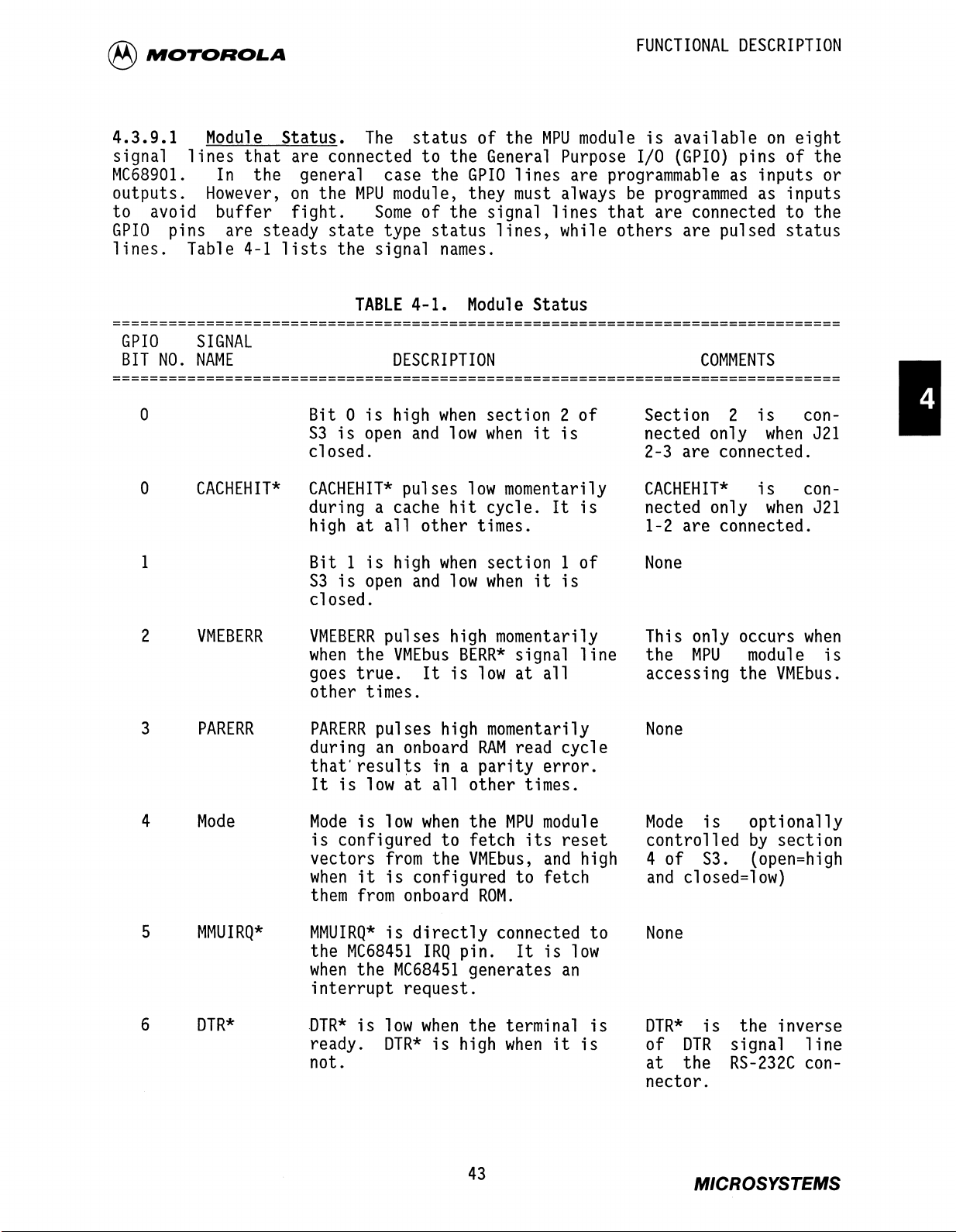
®
MOTOROLA
FUNCTIONAL
DESCRIPTION
4.3.9.1
signal
MC68901.
outputs.
to avoid buffer
GPIO
lines.
==============================================================================
GPIO
BIT
NO.
==============================================================================
o
o
1
Module
lines
In
However,
Status.
that
are connected to the
the general case the
on
fight.
pins are steady
Table
4-1
lists
SIGNAL
NAME
Bit 0
S3
closed.
CACHEHIT*
CACHEHIT*
during a cache
high
Bit 1
S3
The
the
MPU
Some
state
type
the signal
TABLE
is
is
open
at
all
is
is
open
status
GPIO
module,
they
of the signal
status
names.
4-1.
DESCRI
high
and
pulses
Module
PTION
when
low
low
hit
other times.
high
when
and
low
of the
General
MPU
lines
must
Purpose
are
always
lines
lines,
while others are pulsed
Status
section 2 of
when
it
is
momentarily
cycle.
It
section 1 of
when
it
is
module
is
I/O
programmable
be
programmed
that
are connected to the
Section 2
nected only
2-3
CACHEHIT*
is
nected only
1-2
None
available
(GPIO)
pins of the
as
inputs or
as
COMMENTS
is
are connected.
is
are connected.
closed.
on
eight
inputs
status
when
when
con-
J21
con-
J21
2
3
4
5
6
VMEBERR
PARERR
Mode
MMUIRQ*
DTR*
VMEBERR
when
goes
pulses
the
true.
VMEbus
It
other times.
PARERR
during
that'results
It
Mode
is
vectors
when
them
MMUIRQ*
the
when
interrupt
DTR*
ready.
pulses
an
high
onboard
tn
is
low
at
all
is
low
when
configured to fetch
from
the
it
is
configured to fetch
from
onboard
is
directly
MC68451
the
IRQ
MC68451
request.
is
low
when
DTR*
is
not.
high
momentarily
BERR*
is
low
signal
at
momentarily
RAM
read cycle
a parity
other times.
the
MPU
its
VMEbus,
ROM.
connected to
pin.
It
generates
the terminal
high
when
line
all
error.
module
reset
and
high
is
low
an
is
it
is
This only occurs
the
accessing the
MPU
module
VMEbus.
None
Mode
controlled
4 of
and
is
optionally
by
S3.
(open=high
closed=low)
section
None
DTR*
of
at
is
DTR
the
the inverse
signal
RS-232C
nector.
when
is
line
con-
43
Artisan Technology Group - Quality Instrumentation ... Guaranteed | (888) 88-SOURCE | www.artisantg.com
MICROSYSTEMS
Page 53

@MOTOROLA
FUNCTIONAL
DESCRIPTION
II
TABLE
==============================================================================
GPIO
BIT
==============================================================================
7
7
==============================================================================
NOTE:
==============================================================================
4.3.9.2
various functions.
location
SIGNAL
NO.
NAME
ACFAIL:
SYSFAIL:
Only
software monitoring. But, there are
(TAS
treat
and
recovery
VMEBERR,
on
the presence of
MMUBERR
Module
F40000
ACFAIL*
from
SYSFAIL*
from
dual
as
RTE
that
Control Register.
The
and
are defined
4-1.
DESCRIPTION
is
the
VMEbus.
is
the
VMEbus.
PARERR,
port lock
a
"soft
reruns the
control
Module
the
ACFAIL*
the
SYSFAIL*
and
MMUBERR
and
local
BERR
exception
bus
error"
bus
register
as
shown
Status (cont'd)
signal
signal
status
two
bus
time-out).
and
and
should
cycle.
The
MCR
below:
provides software control for
bits
COMMENTS
This
1-2
This
2-3
bits
other sources of
absence of
use
(outputs) are accessed
is
only
are connected.
is
only
are connected.
are available for
The
software should
VMEBERR,
the
normal
when
when
bus
errors
PARERR,
hardware
J2
J2
at
+--------+--------+--------+--------+--------+--------+--------+--------+
I
BIT
7 I
BIT
6 I
BIT
5 I
BIT
4 I
BIT
3 I
BIT
2 I
BIT
1 I
BIT
° I
+--------+--------+--------+--------+--------+--------+--------+--------+
I
Wwp* I ALTCLR*I
FREEZE I CACHEN I PAREN* I IE*
I
CTS*
IBRDFAIL
I
+--------+--------+--------+--------+--------+--------+--------+--------+
BIT
7 -
BIT
BIT
BIT
WWP*,
good
the
when
Correct
6 -
ALTCLR*,
interrupt
interrupt
from
5 -
When
writes to
space).
freezing the cache
from
4 -
When
hits
restrictions
when
onboard
same
1,
parity
starting
FREEZE
occurring.
CACHEN
can
0,
RAM
location
allows correct
when
mode.
mode
the
is
cached
When
FREEZE
is
occur.
imposed
causes faulty parity to
location
is
is
defined
1, allows
When
ALTCLR*
(if
alternate
1, the cache cannot
locations invalidate then
is
does
0,
the cache cannot
When
by
is
written to
read, a
parity
as
bus
in
effect),
0,
not necessarily prevent cache
CACHEN
the
parity
being
error
is
interrupt
cache
can
is
FREEZE
to
0,
be
odd.
to
it
and
be
be
1,
bit.
be
stored
by
error
written
start
stops the
disables
mode.
be
updated (except
updated.
updated
cache
is
when
the
MPU.
occurs.
by
the
the
alternate
alternate
bus
errors
if
in
same
Note
and
no
enabled with
any
When
WWP*,
MPU.
FC2
that
hits
cache
44
Artisan Technology Group - Quality Instrumentation ... Guaranteed | (888) 88-SOURCE | www.artisantg.com
MICROSYSTEMS
Page 54

®MOTOROLA
BIT
BIT
BIT
BIT
3 -
When
because of
0,
2 -
When
When
1 -
When
When
0 -
When
driven
lit.
the
The
at
PAREN*
they can,
IE*
IE*
CTS*
CTS*
BRDFAIL
low
When
MPU
module.
is
parity
if
is
1,
is
0,
interrupt
is
is
1,
is
by
BRDFAIL
1,
errors
parity
no
interrupt
0,
the
the
CTS
1, the
the
MPU
is
bus
is
0,
contents of the control
the
same
address.
FUNCTIONAL
error
in the onboard
exceptions
RAM.
can
not occur
When
enabled in hardware.
requests reach the processor.
requests reach the processor.
CTS
line
to
line
SYSFAIL*
module,
the
register
the terminal
is
to the terminal
line
and
the
SYSFAIL*
is
are readable
on
the
FAIL
not driven
is
is
VMEbus
indicator
DESCRIPTION
it
is
true.
false.
is
is
low
by
4.3.9.3
Timers.
each timer
refer
to
the
Timer
Timer
Timer
Timer
The
XTAL
MHz
baud
input to the
module
rate
Immediately
are
set
Four
is
capable of generating
MC68901
C -
Baud
Data
rate
A - Software
after
to logic 1
reset,
by
hardware.
all
control
timers are provided onboard through the
an
interrupt.
Sheet.
generator for the
tick
timer.
The
timers are assigned as follows:
serial
port.
B - Tick timer overflow/watchdog time-out.
D -
Delay
and
timer are
mode
The
only - unassigned
watchdog
module
MC68901
2.5
MHz
programmable
when
for
time-out
timer B output
is
MPU
clock divided
10
MHz
module).
via
timerC
by
resets
The
as
hardware.
the
is
shown
register
For
detailed
MPU
set.
by
four (3.125
baud
rates
below:
bits
MC68901,
information
MHz
supported
and
for 12.5
by
the
45
Artisan Technology Group - Quality Instrumentation ... Guaranteed | (888) 88-SOURCE | www.artisantg.com
MICROSYSTEMS
Page 55

®
MOTOROLA
FUNCTIONAL
DESCRIPTION
I
I I 12.5
I I
IBAUD
IRATE
THEOR.
16 X CLOCK I SCALE
FREQI
PRE
MHz
MODULE
XTAL
= 3.125
TIMER C ACT
COUNT
FREQ
MHz
ERRORI
PRE
SCALE
10
MHz
MODULE
XTAL
TIMER C ACT
= 2.5
COUNT
MHz
FREQ
I
I
I
ERRORI
+-----------------+----------------------------+----------------------------+
19600
1 I 1
14800
1 1 1
12400
1 1 1
11200
1 1 1
600
1
1 1 1
1
300
1 1 1
110
1
153600
76800
38400
19200
9600
4800
1760
I
10
1 4 5
1 4
1 4
1 4
1 4
1
16
1
10
20
41
81
55
156250
78125
39063
19531
9527.8
4823.5
1775.9
1.7 4 2
1.7 4 4
1.7 4 8
1.7 4
4
4
10
16
33
65
71
156250
78125
39063
19531
9470
4807.2
1760.6
1.7 1
1.7 1
1.7 1
1.7 I
1.4 1
1
.031
+-----------------+----------------------------+----------------------------+
4.3.10
Two
support
64K
positions
ROM
28-pin
x 8 28-pin
ROM
4K
on
x 8
headers.
sockets for user-supplied
and
8K
x 8 24-pin devices,
parts.
Configurations
for
ROM/EPROM
and
the devices
are provided.
8K
x 8,
16K
may
x 8,
be
The
32K
chosen
sockets
x 8,
by
jumper
and
The
However,
position (disabled)
pointer
to
4.3.11 Source
There are several sources of
while others are not.
error
the
are
as
processor rerun.
4.3.11.1
error
a
has
ROM/EPROM
when
and
program
ROM
do
not cause a
of
came
MSR.
no
bus
benign,
exception occurs
VMEbus
attained
from.
The
other sources are not.
error
and
VMEbus
access
VMEbus
is
normally accessed as
the
module
prior
counter
bus
error
Bus
Error Exceptions
The
All
the
status
the
BERR.
by
bits
bus
error
VMEbus
when
the
MPU
mastership.
shown
is
reset,
to the
from
potentially
the
module.
the
exception to occur.
bus
errors.
MSR
can
set
in the
service routine should execute
BERR
VMEbus
if
reset,
first
Some
be
fatal
When a bus
MSR,
is a status
BERR*
This
can
in the
the
the
eight bytes
of the sources are
read to determine
error
then the
signal
only
memory
mode
error
switch
MPU
fetches
of
sources are
error
bit
line
happen
onboard
has
occurred,
in the
is
driven
after
map
in Chapter 3.
is
in the
its
reset
ROM.
fatal
what
should
an
source a
status
RTE
MSR.
true
the
MPU
normal
stack
Writes
errors
bus
bits
in
if
there
be
treated
to cause a
This
bus
during
module
46
Artisan Technology Group - Quality Instrumentation ... Guaranteed | (888) 88-SOURCE | www.artisantg.com
MICROSYSTEMS
Page 56

@MOTOROLA
FUNCTIONAL
DESCRIPTION
4.3.11.2
MSR.
This
On
board
bus
Parity
error
encountered in the onboard
in
RAM
can
be
the
WWP
bit
4.3.11.3
bit.
This
execution
true
Dual
bus
of
caused
in the
Port
a
by
MCR,
Lock
error
TAS
instruction.
with a processor rerun.
4.3.11.4
available
MMU
drives
4.3.11.5
bus
error
alloted
MMU
as
time.
Fault.
status
its
Local
FAULT*
in the
pin
Bus
Time-out.
exception occurs
Local
bus
Error.
Onboard
exception occurs
RAM
while
uninitialized
or
on
lAS
by
a data
Error.
parity
RAM
Dual
exception occurs
MMU
MMU.
This
fault
This
is
is
not a
bus
low.
Local
when
bus
VMEbus
time-out should
parity
when
is
after
failure
when
not a
error
time-out
be
rerun with a processor rerun.
error
is a status
a location with
enabled in the
power-up, a write
in the
port lock
a
fatal
status
RAM.
on
retry
error
bit
exception occurs
is
not a
mastership
is
bad
MCR.
TAS
is
not a
happens during the
and
should rerun
in the
whenever
status
not
attained
bit
parity
Bad
to
RAM
MSR,
bit.
in the
is
parity
with
status
but
is
the
This
in the
If
a local
bus
time-out occurs
port access occurs, the
system should
not
VMEbus
bus
happen
from
timeout
be
at
the
the
on
module.
the module.)
organized
end
at
the
same
MPU
response
such
that
time
may
be
dual port accesses
that
undefined.
a dual
The
of long periods of withholding the
(Long
period = the selected local
do
47
Artisan Technology Group - Quality Instrumentation ... Guaranteed | (888) 88-SOURCE | www.artisantg.com
MICROSYSTEMS
Page 57

II
([!yMOTOROLA
FUNCTIONAL
DESCRIPTION
THIS
PAGE
INTENTIONALLY
LEFT
BLANK.
48
Artisan Technology Group - Quality Instrumentation ... Guaranteed | (888) 88-SOURCE | www.artisantg.com
MICROSYSTEMS
Page 58

7
6
5
4
3
o
c
'-------,---
L-
____
HAL
RUN
RESET
-,
T,F
\~L.
]
L.:u'S
SWITCH
________
MPU
_
LOCAL
CACHE
BUS
ARBITRATION
BUS
MMU
MODE
MAP
SWITCHES
DECODER
r'--
DUAL
PORT
CONTROLLER
RAM
_____
REQUEST
DUAL
~
REFRESH
PORT
REFRESH
REQUEST
DUAL
MAP
DECODER
L-r-------r---.--
TIM~
PORT
PI
r-
o
c
RAM
CONTROL
TRANSLATED
ADDRESS
ADDRESS
DATA
CONTROL
,-_+----_+--~_+----_+--~----~~------~S=E~LE~C~T~B~U~S~~--------~_r_r~~._-L--------
BUS
BUS
BUS
BUS
VME
BUS
INTERFACE
____
ADDRESS
DATA
-r--1~~--------------~'-~C~O~N~T~RO~L~B~U~S~
BUS
BUS
B
A
o
~
..J
«
it:
UJ
(/)
I
JI
-
1--
__
SERIAL
INTERRUPT
-1
STATUS
7
PORT.
HANDLER,
REGISTER
TIMERS
1-
___
-----------------
6
CONTROL
REGISTER
ABORT
SWITCH
5
t
ROM/PROM
IEPROM
SOFTWARE
READABLE
SWITCHES
4
FIGURE
4-1.
VME
BUS
REOUESTOR
IRO
AND
63DW)?Q38
MPU
Module
STATUS
BLOCK
REV
Block
BUS
DIAGRAM
8
SH
Diagram
2
OF 15
49/50
B
A
Artisan Technology Group - Quality Instrumentation ... Guaranteed | (888) 88-SOURCE | www.artisantg.com
Page 59

@MOTOROLA
SUPPORT
INFORMATION
CHAPTER
SUPPORT
5.1
This chapter provides the interconnection
The
INTRODUCTION
location
5.2
MPU
5.2.1
Connector
Motorola
each
connector.
illustration,
INTERCONNECT
module
Connector
VMEbus
pin connection, signal
and
schematic diagram for the
SIGNALS
interconnects with the
PI
Interconnect Signals
PI
is
a standard
specifications
DIN
41612
are
mnemonic,
5
INFORMATION
VMEbus
triple
met
by
and
signals,
through connector Pl.
row,
96
the
MPU
signal
parts
MPU
module.
pin
male
module.
characteristic
list
connector.
Table
with parts
All
5-1
lists
for the
I
TABLE
==============================================================================
PIN
NUMBER
===================================,===========================================
AI-A8
A9
AID
All
A12
A13
A14
SIGNAL
MNEMONIC
000-007
GND
GND
DS1*
DSO*
WRITE*
5-1. Connector
DATA
bidirectional data
path
GROUND
Not
GROUND
DATA
that
008-015.
DATA
that
000-007.
WRITE
specifies
bus
between
used.
STROBE
indicates a data
STROBE
indicates a data
- signal driven
PI
Interconnect Signals
SIGNAL
(bits
the direction of data
NAME
AND
DESCRIPTION
0-7) - eight of
lines
VMEbus
1 - signal driven
0 - signal driven
master
that
and
transfer
transfer
by
VMEbus
16
three-state
provide the data
slave.
by
VMEbus
on
data
by
on
data
transfers.
bus
VMEbus
bus
master
master
lines
master
lines
that
A15
GND
Artisan Technology Group - Quality Instrumentation ... Guaranteed | (888) 88-SOURCE | www.artisantg.com
GROUND
51
MICROSYSTEMS
Page 60

®MOTOROLA
SUPPORT
INFORMATION
I
TABLE
==============================================================================
PIN
NUMBER
==============================================================================
Al6
Al7
Al8
Al9
A20
SIGNAL
MNEMONIC
DTACK*
AS*
5-1. Connector
GND
GND
IACK*
PI
Interconnect Signals (cont'd)
SIGNAL
DATA
VMEbus
available
that
during a write cycle.
GROUND
ADDRESS
signal,driven
address
GROUND
INTERRUPT
VMEbus
acknowledge
interrupted
acknowledging
service routine.
TRANSFER
slave
on
data
has
STROBE
is
present
ACKNOWLEDGE
master
NAME
ACKNOWLEDGE
that
the data
been
- the
by
VMEbus
on
that
cycle. A
on
one
the specific
AND
DESCRIPTION
- signal driven
indicates
bus
during a read cycle, or
accepted
falling
master, indicates a valid
the address bus.
- signal driven
indicates a
of
seven
that
VME
interrupt
valid data
from
master
the data
edge
VME
levels
bus
of
this
by
interrupt
has
and
been
is
with a
by
is
the
now
A21
A22
A23
A24
A25
IACKIN*
IACKOUT*
AM4
A07
A06
A26
A27
A28
INTERRUPT
form
signal
INTERRUPT
form
signal
ADDRESS
lines driven
additional information about the address bus,
as
size,
master
ADDRESS
driven
the
memory
ADDRESS
A05
ADDRESS
A04
ADDRESS
A03
ADDRESS
ACKNOWLEDGE
a daisy-chained
is
connected
ACKNOWLEDGE
a daisy-chained
is
connected
MODIFIER
cycle type, and/or data
identification.
bus
(bit
by
VMEbus
map.
bus
(bit
bus
bus
bus
(bit
by
7) -one
master
6) -
(bit
(bit
(bit
IN -IACKIN*
acknowledge.
directly
OUT -IACKIN*
acknowledge.
directly
4) -one
VMEbus
that
same
5) -same
4) -same
3) -same
to
to
master
of
23
specify
as
A07
as
as
as
and
The
IACKOUT*.
and
The
IACKIN*.
of the
three-state
on
A07
A07
A07
three-state
that
transfer
an
address
pin
A24.
on
pin
on
pin
on
pin
IACKOUT*
IACKIN*
IACKOUT*
IACKOUT*
provide
such
bus
lines
in
A24.
A24.
A24.
A29
Artisan Technology Group - Quality Instrumentation ... Guaranteed | (888) 88-SOURCE | www.artisantg.com
A02
ADDRESS
52
bus
(bit
2) -same
as
A03
on
pin
MICROSYSTEMS
A28.
Page 61

®
ItIIOTOROLA
SUPPORT
INFORMATION
TABLE
==============================================================================
PIN
NUMBER
==============================================================================
A30
A31
A32
Bl
B3
B4
SIGNAL
MNEMONIC
AOI
-12
+5
BBSY*
B2
ACFAIL*
BGOIN*
5-1.
VDC
VDC
Connector
ADDRESS
-12
MPU
+5
MPU
BUS
module
Not
AC
failure
BUS
bus-grant-out a daisy-chained
received
module
three bus-grant-in lines are connected
their
PI
Interconnect Signals (cont'd)
SIGNAL
bus
Vdc
Power -used
module.
Vdc
Power -used
module.
BUSY -this
is
the
used.
FAILURE
has
occurred.
GRANT
at
may
respective bus-grant-out
NAME
AND
(bit
1) -same
by
by
signal
bus
master.
- Input signal
(bit
the
become
0)
jumpered
the
is
bus
DESCRIPTION
as
the logic
the logic
driven
that
IN
level indicates the
master.
A03
on
pin
A28.
circuits
circuits
low
when
indicates a
- bus-grant-in
bus
grant. A grant
The
lines.
the
remaining
directly
on
the
on
the
MPU
power
and
MPU
to
I
B5
B6
B7
B8
B9
BI0
B11
BGOOUT*
BGlIN*
BGlOUT*
BG2IN*
BG20UT*
BG3IN*
BG30UT*
BUS
bus-grant-out
When
level
the bus-grant-out signal
1
BUS
BUS
BUS
BUS
BUS
BUS
evel
GRANT
GRANT
GRANT
GRANT
GRANT
GRANT
GRANT
a bus-grant-in
and
.
the
(bit
(bit
(bit
(bit
(bit
(bit
(bit
form
MPU
IN -same
1)
1)
OUT -same
IN -same
2)
2)
OUT -same
3)
IN -same
3)
OUT -same
0)
a daisy-chained
is
not awaiting
OUT
is
received
is
- bus-grant-in
bus
at
the
bus
mastership,
true
as
as
as
on
BGOIN*
as
BGOOUT*
BGOIN*
as
BGOOUT*
BGOIN*
as
BGOOUT*
the respective
on
on
on
grant.
jumpered
pin
on
pin
pin
on
pin
pin
on
pin
and
B4.
B5.
B4.
B5.
B4.
B5.
53
Artisan Technology Group - Quality Instrumentation ... Guaranteed | (888) 88-SOURCE | www.artisantg.com
MICROSYSTEMS
Page 62

®
MOTOROLA
SUPPORT
INFORMATION
I
TABLE
==============================================================================
PIN
NUMBER
==============================================================================
BI2-BIS
B16-B19
B20
B21,B22
B23
B24-B30
B31
5-1. Connector
SIGNAL
MNEMONIC
BRO*-BR3*
AMO-AM3
GND
GND
IRQ7*IRQl*
PI
Interconnect Signals (cont'd)
SIGNAL
BUS
REQUEST
jumpered level
mastership.
true
ADDRESS
A23.
GROUND
Not
GROUND
in the
used.
INTERRUPT
interrupt
seven
Not
is
used.
When
ROR
MODIFIER
REQUEST
request inputs.
the highest
NAME
(0-3) - the
mode,
AND
DESCRIPTION
is
true
one
(bits
when
or
more
bus
mastership
0-3) -
(7-1) seven
priority.
bus
request
the
MPU
bus
request
same
Jumper
requires
is
released.
as
AM4
prioritized
enabled, level
at
lines
on
the
bus
is
pin
B32
CI-C8
C9
CI0
Cll
C12
+S
VDC
D08-DOIS
GND
SYSFAIL*
BERR*
SYSRESET*
+S
Vdc
Power
DATA
bidirectional data
path
GROUND
SYSTEM
fail
MSR.
BUS
slave
a data
SYSTEM
input signal
the
bus
between
FAIL
bit
ERROR -an
that
transfer
RESET
MPU
module.
-same
(bits
VMEbus
- signal driven
is
true in
active
indicates
cycle.
- the system
that
as
+S
VDC
on
pin
8-1S) - eight of
lines
master
MCR.
an
causes a
that
and
slave.
by
the
Also
low
error
can
signal driven
has
controller
module
provide the data
A32.
16
three-state
MPU
module
be
monitored
occurred during
provides
level
by
VMEbus
reset
when
in
this
on
S4
Artisan Technology Group - Quality Instrumentation ... Guaranteed | (888) 88-SOURCE | www.artisantg.com
MICROSYSTEMS
Page 63

®MOTOROLA
SUPPORT
INFORMATION
TABLE
==============================================================================
PIN
NUMBER
==============================================================================
C13
C14
C15
C16
C17
C18
C19
C20
SIGNAL
MNEMONIC
AM5
A23
A22
A21
A20
A19
AlB
5-1. Connector
LWORD*
PI
Interconnect Signals (cont'd)
SIGNAL
LONGWORD
remains
master.
VMEbus
ADDRESS
ADDRESS
ADDRESS
ADDRESS
ADDRESS
ADDRESS
ADDRESS
- not driven. This terminated signal
at a high
The
accesses
MODIFIER
bus
bus
bus
bus
bus
bus
dual
when
(bit
(bit
(bit
(bit
(bit
(bit
NAME
AND
DESCRIPTION
level
(bit
23) -same
22) -same
21) -same
20) -same
19) -same
18) -same
when
port
LWORD*
5) -same
the
RAM
does
is
true.
as
A07
as
A07
as
A07
as
A07
as
A07
as
A07
MPU
module
not respond to
as
AM4
on
on
pin
on
pin
on
pin
on
pin
on
pin
on
pin
is
pin
A24.
A24.
A24.
A24.
A24.
A24.
bus
A23.
I
C21
C22
C23
C24
C25
C26
C27
C28
C29
C30
C31
==============================================================================
A17
A16
A15
A14
A13
A12
All
AI0
A09
A08
+12
VDC
ADDRESS
ADDRESS
ADDRESS
ADDRESS
ADDRESS
ADDRESS
ADDRESS
ADDRESS
ADDRESS
ADDRESS
+12
MPU
bus
bus
bus
bus
bus
bus
bus
bus
bus
bus
Vdc
module.
(bit
17) -same
(bit
16) -same
(bit
15) -same
(bit
14) -same
(bit
13) -same
(bit
12) -same
(bit
11) -same
(bit
10) -same
(bit
9) -same
(btt
8) -same
Power -used
as
as
by
the logic
as
as
as
as
as
as
as
as
A07
A07
A07
A07
A07
A07
A07
A07
A07
A07
on
pin
on
pin
on
pin
on
pin
on
pin
on
pin
on
pin
on
pin
on
pin
on
pin
circuits
A24.
A24.
A24.
A24.
A24.
A24.
A24.
A24.
A24.
A24.
on
the
55
Artisan Technology Group - Quality Instrumentation ... Guaranteed | (888) 88-SOURCE | www.artisantg.com
MICROSYSTEMS
Page 64

®MOTOROLA
SUPPORT
INFORMATION
I
5.2.2 Terminal Port Connector
A standard
detailed
connection, signal
The
VME120
to connect
Ready
This allows the system to
The
controlled
controlled
sensed
data sheet for
==============================================================================
==============================================================================
(DSR),
VME120
by
PIN
NUMBER
1
RS-232C
information
mnemonic,
has
only a
it
to a
Data
Carrier Detect
also
by
software to
by
bit
can
bit
6 of the
details.
TABLE
SIGNAL
MNEMONIC
cable
on
partial
modem.
tell
detect a
clear
1 of the
IPRA
5-2. Connector
Jl
mates
RS-232C
and
signal
RS-232C
As
(DCD)
the terminal
Data
buffers or
module
in
the
Not
used.
Interconnect Signals
with connector J1. Refer to
interfacing.
characteristic
implementation.
wired,
SIGNAL
it
signals,
Terminal
send
control
MK68901
Jl
Interconnect Signals
NAME
provides permanently
when
peripheral chip. Refer to
Table 5-2
for the connector.
No
facility
and a programmable
it
is
ready to transmit data.
Ready
a message,
register
AND
(DTR)
DESCRIPTION
signal,
if
at
F40000,
Appendix
lists
is
true
CTS
that
desired.
and
A for
each
provided
Data
pin
Set
signal.
can
be
CTS
is
DTR
is
Mostek
2
3
4
5
6
7
8
9-19
20
TxD
RxD
CTS
DSR
SIG-GND
DCD
DTR
TRANSMIT
on
this
RECEIVE
presented to the terminal.
Not
CLEAR
terminal
permissible to begin transmission of a message.
DATA
MVME120
MVME120
SIGNAL
DATA
the terminal to enable
Not
DATA
the
send
to
DATA
line
DATA
used.
TO
SET
is
GROUND -common
CARRIER
used.
TERMINAL
MVME120
or receive data.
- data to
to the
- data
SEND -CTS
by
the
READY -DSR
to the terminal to indicate
ready to transmit data.
DETECT
READY
indicating
be
MVME120.
from
is
a function supplied to the
MVME120,
- a signal
that
is
a function supplied
return for
- furnished
its
that
transmitted
the receive
indicates
all
by
receive
circuits.
from
the terminal
the terminal to
is
furnished
that
that
signals.
the
MVME120
line
by
is
is
it
is
the
the
to
ready
21-25
==============================================================================
Artisan Technology Group - Quality Instrumentation ... Guaranteed | (888) 88-SOURCE | www.artisantg.com
Not
used.
56
MICROSYSTEMS
Page 65

®MOTOROLA
SUPPORT
INFORMATION
5.3
Table 5-3
noted.
printing.
PARTS
illustrated
These
LIST
lists
in Figure 5-1. Parts
the
parts
components
reflect
TABLE
5-3.
the
of the
listed
latest
MPU
Module
MPU
module.
are for
all
issue of hardware
Parts
The
versions unless otherwise
List
parts
locations are
at
the time of
==============================================================================
REFERENCE
DESIGNATION
==============================================================================
CR1
C1,C6,C26,
C28,C67,C71
C2,C4,C5,
C7-C17,C19C22,C24,C25,
C27,C29-C49,
C51-C53,C55C66,C68
MOTOROLA
PART
84-W8293B01
48NW9616A03
23NW9618A71
21NW9632A03
NUMBER
DESCRI
Printed wiring board
Diode,
Capacitor,
Capacitor, fixed, ceramic, 0.1
1N4148/1N914
electrolytic,
PTI
ON
47
uF @ 10
Vdc
uF @ 50
Vdc
I
C23
DLl
DL2
DL3
DS1,DS2
DS3
J1
J2,J9,J17 ,
J21,J24
J3,J4
J5,J6,J20
J7
23NW9704A99
01NW9804C33
01NW9804C12
01NW9804c34
48NW9612A49
48NW9612A59
28NW9802F88
28NW9802D04
28NW9802C63
28NW9802D01
28NW9802C36
Capacitor, tantalum,
Delay
Delay
Delay
Indicator,
Indicator,
Connector, 25-pin
Header, single
Header, double
Header, double
Header, double
module,
module,
module,
LED,
LED,
triple,
triple,
triple,
red
green
row
row
row
row
33
uF @ 15
40
ns
20
ns
70
ns
post, 3-pin
post, 12-pin
post, 2-pin
post, 14-pin
Vdc
57
Artisan Technology Group - Quality Instrumentation ... Guaranteed | (888) 88-SOURCE | www.artisantg.com
MICROSYSTEMS
Page 66

®MOTOROLA
SUPPORT
INFORMATION
I
TABLE
==============================================================================
REFERENCE
DESIGNATION
==============================================================================
J8
J22
J25
PI
R1
R2
R3,R4
R5
R6
R7,R2l,R23,
R25
MOTOROLA
PART
28NW9802B34
28NW9802C43
28NW9802B2I
28NW9802E5I
51NW9626A37
06SW-124A18
06SW-124A23
06SW-124A25
06SW-124A97
5lNW9626A49
5-3.
NUMBER
MPU
Module
Header, double
Header, double
Header,
Connector, 96-pin
Resistor network, 9/10k
Resistor, fixed,
Resistor, fixed, fi
Resistor, fixed, film,
Resistor,
Resistor network,
Parts List (cont'd)
DESCRIPTION
row
post,
row
post, 8-pin
double
fixed, film,
row
film,
post,
1m,
7/10k
I6-pin
6-pin
ohm
ohm,
51
82
ohm,
100
lOOk
ohm
ohm,
ohm,
5%,
5%,
5%,
5%,
1/4 W
1/4 W
1/4 W
1/4 W
R8,R29
R9
RIO
Rll
R12
R13
R14
R15
R16
R17
R18
R19,R20
R22
5lNW9626A22
51NW9626A4l
51NW9626B55
5INW9626B52
51NW9626A63
51NW9626B56
5lNW9626B51
5lNW9626B49
06SW-124A17
29NW9805B44
5lNW9626B50
51NW9626B48
06SW-124A73
Resistor network, 5/10k
Resistor network, 9/4.7k
Resistor network,
Resistor network,
Resistor network,
Resistor network,
Resistor network,
Resistor network,
Resistor, fixed, film,
Jumper, 2-pin
Resistor network,
Resistor network,
Resistor, fixed, film,
male
9/4.7k
5/l0k
5/2.2k
9/l0k
5/lk
9/l5k
3/47
5/47
ohm
47
ohm
ohm
10k
ohm
ohm
ohm
ohm
ohm
ohm
ohm
ohm,
ohm,
5%,
5%,
1/4 W
1/4 W
R24,R26
Artisan Technology Group - Quality Instrumentation ... Guaranteed | (888) 88-SOURCE | www.artisantg.com
06SW-124A4l
Resistor, fixed,
58
fi
1m,
470
ohm,
MICROS
5%,
1/4 W
YS
TEMS
Page 67

([!jMOTOROLA
SUPPORT
INFORMATION
TABLE
==============================================================================
REFERENCE
DESIGNATION
==============================================================================
R27,R28
R30
SI,S2
S3
Ul,U45,U46
U2,U5,UI0,
U19
U3,U8
U4,U9
U6
PART
06SW-124A83
06SW-124A42
40NW9801A54
40NW9801B29
51NW9615K66
51NW9615G07
51NW9615Hll
51NW9615G47
51NW9615F79
5-3.
MOTOROLA
NUMBER
MPU
Module
Resistor, fixed, film,
Resistor, fixed, film,
Switch, push,
Switch, piano, 4
I.C.
I.C.
I.C.
I.C.
I.C.
Parts List (cont'd)
DESCRIPTION
momentary
74F32PC
SN74S244N
SN74LS645N
MC6882L
SN74S240N
27k
510
SPOT
position,
ohm,
ohm,
SPST
5%,
5%,
1/4 W
1/4 W
I
U7
Ull,
U18
U12
U13,U14
U15
U16
U17,U22
U20
U21
U23
U24,U29,U32
U25,U66,UI0l
U26
(NOTE)
51NW9615F85
51NW9615N76
51NW9615K98
51NW9615G38
(NOTE)
51NW9615K18
51NW9615E93
(NOTE)
51NW9615C30
51NW9615R26
51NW9615K73
51NW9615N04
I.C.
programmed
I.C.
SN74S38N
SN74LS652NT
I.C.
I.C.
74F280PC
I.C.
SN74LS38N
I.
C.
programmed
I.C.
74F373PC
I.
C.
SN74LS14N
I.
C.
programmed
I.
C.
SN74LS193N
I.C.
SN74ALS645-1N
I.C.
74FOOPC
I.C.
MC68451RI0
(used
on
120,
121)
U26
U27
01-W3288BOI
51NW9615N03
Artisan Technology Group - Quality Instrumentation ... Guaranteed | (888) 88-SOURCE | www.artisantg.com
MMU
bypass (used
I.C.
MC68010RI0
59
on
(used
122,
on
123)
120,
121)
MICROSYSTEMS
Page 68
@MOTOROLA
MPU
TABLE
==============================================================================
REFERENCE
DESIGNATION
==============================================================================
PART
5-3.
MOTOROLA
NUMBER
Module
Parts List (cont'd)
DESCRIPTION
SUPPORT
INFORMATION
I
U27
U28
U30,U33,U36,
U43,U64,U72,
U76,U77,U81,
U82,U87,U93,
U99,
UlOO,
U106
U31
U34
U3S
U37
U38
U39
U40
51NW9615Rll
(NOTE)
SlNW9615J39
(NOTE)
(NOTE)
SlNW9615N40
51NW9615F30
SlNW961SD93
(NOTE)
(NOTE)
I.
C.
MC68010R12
programmed
I.C.
I.C.
74F74PC
programmed
I.e.
programmed
I.e.
I.C.
MC68901
DM74S05N
I.C.
I.C.
SN74S30N
programmed
I.
C.
programmed
I.
C.
(used
on
122,
123)
U41,U49
U42,U83,U9S,
U107
U47
U48,U59
U50,US1,U53
US4
USS,U70
US6
US7
US8,U88
SlNW9615H79
SlNW9615K70
SlNW961SL74
SlNW961SN32
51NW961SN4S
SlNW961SK6S
SlNW961SK71
(NOTE)
SlNW961SK69
SlNW961SK72
I.C.
TMM2016P-1
74F08PC
I.C.
74Fl63PC
I.
C.
74F164PC
I.
C.
74F257PC
I.C.
I.
C.
74F64PC
I.
C.
74F04PC
programmed
I.
C.
I.
C.
74F10PC
I.
C.
74F92PC
(used
on
120,
121,
123)
60
Artisan Technology Group - Quality Instrumentation ... Guaranteed | (888) 88-SOURCE | www.artisantg.com
MICROS
YS
TEMS
Page 69

®
MOTOROLA
SUPPORT
INFORMATION
TABLE
5-3.
MPU
Module
Parts
List
(cont'd)
==============================================================================
REFERENCE
DESIGNATION
MOTOROLA
PART
NUMBER
DESCRIPTION
==============================================================================
U60,U67,U73,
U78,U84,U90,
U96,U102
U61,U62,U68,
U69,U74,U75,
U79,U80,U85,
U86,U91,U92,
U97,U98,U103,
U104,U109,
UllO
U61,U62,U68,
U69,U74,U75,
U79,U80,U85,
U86,U91,U92,
U97,U98,UI03,
U104,UI09,
UllO
51NW9615N43
51NW9615M09
51NW9615P38
I.C.
TMS2150-5JL
I.C.
MCM6665AP15
I.C.
HM50256-15
(used
(used
(used
on
on
on
120,
120,
121,
121,
122)
123)
123)
I
U63
U65
U7l
U89
U94
U105
U108
VI
VI
51NW9615N47
51NW9615F38
51NW9615K67
51NW9615K68
51NW9615D26
51NW9615B30
(NOTE)
48AW1068B03
48AW1015Bll
09NW9811A78
09NW9811A7l
I.C.
MC3488API
I.C.
SN74LS393N
I.C.
74F20PC
I.C.
74F11PC
I.C.
SN74S113N
I.
C.
MC1489AP
I.
C.
programmed
Crystal
121)
Crystal
123)
Socket,
at
(use
Socket,
at
(use
oscillator,
oscillator,
DIL,
U7,UI6,U21,U28,U31,U40,U56,UI08)
U26,U27)
PGA,
20-pin
68-pin
20.0
25.0
MHz
MHz
(used
(used
on
on
120,
122,
61
Artisan Technology Group - Quality Instrumentation ... Guaranteed | (888) 88-SOURCE | www.artisantg.com
MICROSYSTEMS
Page 70

@MOTOROLA
SUPPORT
INFORMATION
I
TABLE
==============================================================================
REFERENCE
DESIGNATION
==============================================================================
=============================================================================
NOTE:
=============================================================================
When
PART
09NW9811BOI
09-W4659B24
09-W4659BI2
09-W4659BI4
09NW98IIA46
55NW950IAI2
64-W4736BOI
29NW9805BI7
ordering,
5-3.
MOTOROLA
NUMBER
use
MPU
number
Module
Socket,
(use
Socket, 24-pin
(use
Socket, I2-pi n
(use
Socket, I4-pin
(use
Socket,
(use
Handle
Panel, front
Jumper,
JI7,J20,J24,J25)
labeled
Parts List (cont'd)
DESCRIPTION
OIL,
at
U34,U39)
at
U35)
at
U4I,U49)
at
UX44,UX52)
crystal,
at
YI)
24-pin
shorting, insul ated (use
on
part.
4-1ead
at
J2-J9,
62
Artisan Technology Group - Quality Instrumentation ... Guaranteed | (888) 88-SOURCE | www.artisantg.com
MICROSYSTEMS
Page 71

SVtl3.LSA
SOHOIVtl
£9
I
"T1
.....
s:i)
c:::
;:a
IT'I
01
I
......
3:
""C
c:::
3:
0
0-
C
....
Cl)
""C
(l.I
""1
c-t'
(I)
r-
0
()
(l.I
c-t'
......
0
:::l
:'CJCJ
d-
T · U2S
cr-
~
-=--,.
~~
o
iCJ
~CJ
r---I
~f
U2
U7
f U20
l~ulO
~C21
Oll
Ol2
'C,
UII
If
U21
clil
U2I
0 0 f
C20
-
-~UI
c·1
f
UI1
f U22 If
U21 f
C21
U4
zl
f I
CI.'
,
tf=
CI.
UII
c11
U2'
U2.
Uti
UI4
RII
It
I
10m
I
,
a~I~~~~~~~~~~~
D
n
~
- on u U11 c471 f U14
I
~
f-T==F==-{
R21 Ull
CSI
UI1
RU
,..
U1.
~::::::::~~::::::::::~r-----------------hM-----------'-r-----------'
UI2
UII
:=:::=:=:=UIO
~::::::::::::::::~::::::::::~~::::::::::::
r-
~~~
"'I
f
U14
U.O
fC5
fCl'
fm
'"
,,·1 , ..
c·,1
us
U24 ,
A1S
cIO~1
I~~
5
,
I~
U15
L...-...,
NOI1VW~OjNI
l~Oddns
Artisan Technology Group - Quality Instrumentation ... Guaranteed | (888) 88-SOURCE | www.artisantg.com
UI.
UIOO
i
Ul01 UI07
Ul021
If
fcu
Ul01
If
"..,OI:lO.LOW
cill
f
Ul0.
lOS
I
~
GiJ
Page 72

@MOTOROLA
SUPPORT
INFORMATION
I
5.4
SCHEMATIC
FIGURE
5-2
illustrates
DIAGRAMS
the schematic
diagram
for the
MPU
module.
64
Artisan Technology Group - Quality Instrumentation ... Guaranteed | (888) 88-SOURCE | www.artisantg.com
MICROS
YS
TEMS
Page 73

7
6
5
4
3
D
c
8
NOTES:
1.
FOR
REFERENCE DRAWINGS REFER TO
BILL<S)
2.
UNLESS OTHERWISE SPECIFIED:
I.
INTERRUPTED
SAME I_ETTER
ARE
& DEVICE TYPE NUMBER IS FOR REFERENCE
ONL Y. THE NUMBER VARIES WITH THE
MM
'). SPE:::IAL SYMBOL USAGE:
6.
INTDPRET
WITH AMERICAN
INSTITUTE
REVISION.
L~
PART
TilE
FULL
8.
CODE
IS AS FOLLOWS:
OF
MATERIAL
ALL
RESISTORS ARE IN OHMS.
1/4
WATT.
ALL
CAPACITi.'~;S
ALL
VOLTAG~S
LlNES
EL_ECTRICALL Y CONNECTED.
UF
ACTURER.
+ DENOTE:S -
[]
DENOTES -
TYPES
FIELD
PART
FOR
~
------~--
XU52
U110
S3
R30
J25
--
_PL3
CRI
C71
HIGHEST
NUMBER NOT USED
USED
REFERENCE DESIGNATIONS
OR
DI,~GRAM
SPECIFICATIONS. CURRENT
/l.RE
OF
THE DRAWING.
TYPE.
SHEET TO SHEET REFERENCES
Yl
PI
01-
ARE
ARE
CODED
LETTER
ACTIVE
ON
BOARD SIGNAL.
IN ACCORDANCE
NATIONAL
ABBREVIATED
REFER TO
SHEETJ
--
XUI-4345-51
U_4452
CI8,50
546970
W 329.3B01
IN
UFo
DC.
WITH THE
COMBINATIONS
LOW SIGNAL.
STANDARDS
IN
FOR
TABLE
~
ZONE
±5PCT.
1.
&
TABLE
REF
DES
__
J2!.Lr----_4~S
J2L2.
=0.3
UI
_lJ2
~
--U4
U5
~1!6
U7 PAL
~-~=
U10
f---1ilL
UI2
r-JiliL
U14
r--~
~Q
UI7
r-1I-l8
UI9
r-I"J20
f-J.!Z1-
~
__
7"±U2 7
7~'i1.
74LS645
MC6882..S.
74~
74S240
74S244
f--
74S38
71j...~~
74F280
L1.E2.60
_I4LS38
___
PALI6L
74F373
74S38
74~
74LSI4
82S153A
TYPE
~
L6~
r~;;----f:ftl~;
U24
lJ2/i
U26
U26
U26
U27
1,,127
U28
U29
U30
1,,132
U33
U34
U35
1,,137
U38
U39
U40
U41
U42
U43
U45
u'l6..
U47
U48
U49
Us0
U51
U53
74LS645-1
74F00
MC68451
MC68451
MC68451
MC68451
MC68010
MC6S010
PAL
16L2
74:.S645-1
74F74
PiI...L16Ull
74LS64;i-1
74F74
PAL20L8A
MK68901
74F74
7~
74S30
PAL20L3A
PALl6L8B
MCM65116
74F08
74FI1-
74F32
74F32
74F163
74F164
MCM65116
74F2S7
74F257
74F257
J..I.215_
J.Lll
_V::i6
I
&
__
__
8A
GND
+5V
7
_L1.
7 14
7 14 12.13
-.l1...
10
20
10
20
~
20
10
20
10
20
10
2"
::
;:
10
20
-,
14
12
2.4 7
7
__
lL
7
~4
7)4
10_~
10
___
20
7 14 9.11.13
10
20
7 14
10
20
SH
612.13
6.B.l1
3.4.7.8
3.4.12
~
3.8.12~13
4.7
__
JL
3.4.11
4.69.11
~-~T:--~
10
Z0
7 H 4.6.11
AI"
_He 7
J2
C3 7
H3 H9 7
C8 7
E2
_E.I1
09 02
10
20
10
~
7.l.L.
_Hi
20
10
20
7 14 12.15
12
24
36
II
7 14 9
7 14 4.8.11.12
7 14
12
_2~
10
20
12
~46
7 14
7 14
7_J
."1.
8
___
7 14
12
Jl
8
8
14
14
16
24
L6
16
16
47.1112
4.9
3.9.12
4.11
.--l~
?~
12
12
1~
I"
__
11
a
7
11
7
12
4
4
8
12
4
9
i2
7
15
11
15
5
4
12
6
10
HI'
&
TABLE I CON'T
REF
DES
!
U54
U55
1,,156
U57
U58
1,,159
6
r-u
0
1,,161
U62
U63
1,,164
U65
U6B
U67
U68
1,,169
U70
U71
j,a2.
U73
U74
U75
U76
U77
1,,178
U79
~.
1,,181
1.182
U83
4
r-.l.!.f
1,,185
ua6
1,,187
1,,188
U89
1,,190
U..91
un
U93
U94
U95
U96
1,,197
U98
U99
UI00
U101
UI02
r-0~:!
U105
UI06
--.!.!.107
Ul08
U109
UU0
XU44
XU52
YI
TYPE
&
74F64
L~
PALl6R8
74F10
74F02
74F164
TMS2150
M9M3256
MCM6256
.MC..J....488
HEH
~3
74F00
TMS2150
MCM625/i
MQM~2:i6
.B£04
__
~0
74F74
TM~21
:i~
MCM§256
~6
74F74
74F74
IMS2150
MCM6256
MCM6256
74F74
74F74
74F08
TMS2150
MCM6256 . 16
MCM6256
74F74
74F02
74Fll
TMS2150
MCM6256
MCM6256
74F74
74SII~
74F08
TMS2150
MCM6256
MCM6256
74F74
74F74
_71£00_
TMS2150
MCM6256
MCM6256
MCI489
74fH74F08
PAL
16L8A
MCM6256
MCM6256
SOCKET
SOCKET
K
II
00
GND
7
7
10
7
7
7
12
16
16
1.
7
7
7
12
16
16
7
7
7
12-
16
16
7
7
'')
16
16
7
7
7
12
16
7
7
7
12
16
16
7
7
7
12
16
16
7
7
"L
12
16
16
7
L
7
10
16
1Ii
7
t12V
+5V
14
14
20
14
14 7.8.11
14
24
8
8
14
14 8
14
24
-12V
~----
4
UJ.2.LL
89.12
5
8
9.12,1~,I:i
8
8
14
14
14
24
8
8
14
14
24
8
8
14 9
14
14
24
8
8
14
14
14
24
8
8
14
14 8
14 8.13
24
8
8
14
14 8
14
24
8
8
14
1'1.
14
20
8
8
14 4
-
89.13
89
--
69
9JJ
8.13
8,913
II 9
89
3.8,9
SH
I~
L-_
5
10
10
15
11
5
10
10
5
10
10
13
13
5
10
10
13
5
10
10
9
5
10
10
5
10
10
5
10
10
15
8
8,9
6
10
10
14
\4
D
c
B
_.
A
7
6
5
t
Artisan Technology Group - Quality Instrumentation ... Guaranteed | (888) 88-SOURCE | www.artisantg.com
FIGURE
5-2.
MPU
63DW3293B
Module
Schematic
RFV
E SH
Diagram
OF
15
A
65/66
Page 74

7
6
5
4
3
D
c
+
PI
D
~
HAL
RUN
T,F'\IL,
L:::D'S
J
LOCAL
BUS,
ARBITRATION
BUS
MODE
SWITCHES
II
..
r--
__
.L----_._
1
DUAL PORT
CONTROLLER
REFRESH
REQUEST
DUAL PORT REQUEST
REFRESH
TII:'R
l
-.-------L-----
[ESET
JI
r-
SWITCH
-[
MPU
l
-
CACHE
~--+
--+--+--+----+-""'~'-}o---~SE~L~E~C~T~B..;;::U~S=+"'-_-
__
--+_-+---+
__
MMU
TRANSLATED
ADDRESS BUS
ADDRESS BUS
-'.
~I-
__
+-
___
,_-~
___
CONTROL BUS
~~~~~~
DATA
MAP DECODER
BUS
..
·---
rL--
...
:---.:--1----+t---ft-
.....
-\--
....
~~i"----1-L
RAM
______
VME
INTERF
______
--'
RAM CONTROL
BUS
ACE
1-
__
------
-r--.J'---------.-,
r-
I
'-------------------,
DUAL PORT
MAP
DECODE~__
_.+-_....;D;;..;A.;..;T:..:.A.:.....::B;..;;U~S_-1
..
)
,--...:C;.;:O;.;.;N:..:.T..;.;R..;;::O.::.L_...=.BU;;.;S~
.~,
J
ADDRESS BUS
VI
~
ID
lLJ
~
>
c
B
A
o
:::.
~---I
SERIAL
INTERRUPT
STATUS
TIMERS
"'_
7
PORT,
HANDLER,
REGISTER
___________________
1-
___
---------
6
.....;
_____
CONTROL
REGISTER
ABORT
..,...
___________________________
SWITCH
5
t
--
ROM/PROM
!EPROM
-,.
__________
SOFTWARE
READABLE
SWITCHES
FIGURE
5-2.
MPU
REQUESTOR
I:.:.:R~Q
63DW)2~3B
Module
Schematic
VME BUS
. .AND
STATUS
BUS
BLOCK DIAGRAM
REV
8
Diagram
SH
2
OF
15
67/68
B
A
Artisan Technology Group - Quality Instrumentation ... Guaranteed | (888) 88-SOURCE | www.artisantg.com
Page 75

7
6
5
4
3
o
c
_E'.1:..A~
-
.fl::AJ 5
...
fl.=A:Z!O-----.·--j
_fl:.ML-
..
fl::.e.;''--
..
J'L:Ju
_._fL:_QJi
(-
......
Jl:-L-
(-
-El-
(--_n~~.L._.
AlL.
______
~---
-------l
___
r
;JL-_
__
___
___
__
-----1
-12
_
_
t12V
o
IC5
~1
-I
_
_
--rG17
~1
Ic-,}"ii-IC41--Tc4"2-
~1
~1
IC19
~1
IC20
~1
IC43
~1 ~1
TC2I~C22-lc24-IG25
~1
IC44-rc4s--IG4sw
~1
~1 ~1
~1 ~1
~.1
~1
IC27
~1
7
IC48
~1
IC29
~1
IC49
~1
IC7
~1
IC30
~1
IC8
~1
IC31
~1
IC51
~1
IC32
~1
IC52
~1
IC10
~1
IC33
~1
IC53
1'"1
V
V
---Tcs9-Tc61-'Tc62-
~1
~1
'-rC63---IG64I
~1 ~1
~1
C65---Tcs's
IC68
~1 ~1 ~1
I I
3
r r
I I 1
r
ICll
~1
IC34
~1
7 9
r"
Tc12
~1 ~1 ~1
IG35
~1
TC55
~1
~
IC13
IC36 IC37
~1
lCss--IC57
~1
11
12
IC14
IC15
~1
Ic~c39
~1
~1
~1
IC58
~1
IG16-~5V
~916
~1
lC59
~1
C
..
B
".-
A
Jl-15
-
Jl-19
Jl-21
~1~
~-A22~
::~*
T*
I
7
U2E
5244
6
INC
NC
NC
U105A
MC1489
/NC
'2
NC
UllJ58
MC1489
NC
1 R138 1
10K
T T T
3 5 6
NC
R13D 1 R13E
10K
R8A
10K
NC
NC
+ V
2
5
10K
t
NC
1
R14D
1 R15J
lK
T T T T T T
5
NC
10
NC NC NC
15K
5fR17C
47
6
FIGURE
1
3 8
5-2.
R238
10K
1 R25G
10K
NC
MPU
1 R29A 1 R29D
10K
2
NC
63DW
Module
Schematic
10K
5
NC
32938
~~t:!8e,=E;*l
REV
SH
Diagram
4B7.5C7
6C7.7B3
3
OF
..
8
A
15
69/70
Artisan Technology Group - Quality Instrumentation ... Guaranteed | (888) 88-SOURCE | www.artisantg.com
Page 76

7
6 5
4 3
lIB3lPA~EJllil..
o
883
c
..
15C3
B
15B3
1583
15B3
1583
U42B
...
---.-
~;~G)~~_____
_-.----
-~-----.-.
I 1 I
_ .
--
- -
I
~
------------------~~--.-----------.--.-----.
--r
--
l'-----~43A
'---"PR-
D
...
~~R
--
F74
O~
N C
O~----
-----
---
---
R21G
10K
+5v-----
l
"1'1
K1100
L_.a
~1~
OUTI·~'I\.'':'I\--'
LL.-£1-~3-~
8
~----t-~ g~l--v
t--*"-
~~
-~
----CJL~~K
~_L
'-
___
U47
-NC
C
OC~~---l-------------·-------f--+----------------------------
DOD
LD
TCI--L5
PE MCS8010R
NC
CL~_
:=J-
.
~C3CAJ&---_-_----------------------------;-----------------~------------
+ V + V
7C]
CPt)
..
·QL-----'-·--------.,.,U7-::
783
U~.RQ[{lII.L___
E rS!._
,.
U 2
II
4
"J
-L--
B,------,
1
F32,6
./
R4
R8C
10K
4 FAIL HALT
~1~
~~~
)"'---+--
.
82
,.,,@
_L-..
DSI
UIIC
102.~
R3
82
,.,,~~
DS2
,
UIIA
1~
r
U2E
S244
~-fr-..Q~--~,x.!:.SET!-'*"------.Lldll\.')o~:»'-9------jLJ..::I.<
UI5A
L538
l'@IQtt~Q~J
2
19
+ V
~Rl
hN4148
<
R6
;'100K R8E
r-LL.
~IJ
8C3
iliA!"
8D3
Ul!;BB*J
8C3
1I.El...i*J
CIPL1*l
[IEL2*1
lY..P.8*J
_CPT8CK*J
6C3
L~Af1LE*J
383
HJ
'kh~
L~
---
____
ft
._-
~
_
..
"
~
~
~.
________________
~
NC
2
J6
R5
J.
10"
~-'-+--'VV.Ir-L-___,_---1.~~:tn:>-"-~,---'2"-
+ I
C23
++~3
6V
7
~
_______________________________________
U258
4....:...=:..F-....,00
,6
~-----------+-----
+5V'--·1~~~6--,-------~·---~'-----++------------------++-
U20A
L,:>142
l
1/
10K
~-<>-~
D P R 011-",,--5-1-'-
(I>CK
CLR
4
O\r§NC WLI>CK
I
,----
_____
t=
--
-
--,+-+1
U30A U30B
F74
10
112"'-1 D PROW!
O'
CLR
13
.
______________________________
F74
N C
B
~....Jl~
L--------------------+--++-+~~4-~--------~~----------------------+-----
U46D
F32
---
--lbt--
i---
--
-I-----
UF~T--4-:'~1\
-----Ut:)~.L'--;I-A,,'\I'r~2--r--------------------!!IIo-·
R17B
7",7
A'3;--~,...--~--~·--~------------~~'~··------
47
r---
_________
..
_.
_______________________
------- -
U27
----.-.-JO_------
D0~~---~¥
I
+ v
R2
51
____
--.J
_____
,----------------~-li~!T
+rV
2
U37E
IS0~
1 0
U378
__
3_f>~05~.A~=====::::~==:.....j-J
+ V
U37D B 9
r{i;:0>o-5.><..-
8-l.-
+ V
1 RllA I Rl"H
I"K
R13G
10K • 10K
10K
9
I
• RI3H
______
_________________
r-
,---------.p.J.B
r--
____
L-I+_-_1-I-+t---t+-1-+l-t-+I--++-I+_-_-_-_~-_-_-_-_-_-....jtt-_-_-_-.-=----=---=---=---=---=-===========::::'+_
RI0G
+ 5 V'-'1
-,4",7",0,..,0
R10D
00
'U
+5V
l
El
CCK
-*
~
_~HACK
~JJ2H-
H3
lE.l...I'
-.--ll2. m
G2
-
~
NCG,L
NcliL
E
8 A18
1
-1i~i)'f;[(C~K
~8~~
r-%
RLW
r
AS
f-+--------------
8~-'--------1"--)u..)
5
g4
~
g~
ii
DS
A
D~it
Dll R
D12
A
D13
C
D14
R
D15
B
:4
~
A3
1617fl
AS
A 7
(RCA.-
A8 J7
A9 I
A10
fll~1
AI4
J -
A15~
:----
A
16·f-LLL!L.-----"~.u....1
A17
GI0
ft\---
A19
~----h
~2!t
TIT:
A22
CQ
A23
K3
FC0
J3
,FCI
1<2
FC2
U2H
5244
1.7
19~--I--------------II:---~.r~L~D~S*~la:~987
-~.2v
[
[]
~i1;
.....,
~
-lQ
W
~~ifPl
W
-.!
~]
.1
5
/11
~.-------:-
=m,..,
;-..
.8
..
1/1
~
_~il
W~
i~-
~
[All
[AP]
(A
[t2
[A2
[FC0]
1 FCil'\
rFC2N
\
.--.+.
U55E
F04
~
L.
___________
------i_-
.....
I------II
---------+4------------------------
R10E
U25C
.J_ME\J.Q\'Kl
lME'l)ClKlt.1
..
"',.
___
12M1'\,!Gl.Xl
--.lM..P.1i.Q.L.&1l 15C7
_tMf
..
\JQ6.KLel
---W-GJti
[A]
[FC] BUS
lRESI;.I~l
lli.r;~_~.D.
.1QRE.S.Ufl
_____
-----~
[8B/W*J
... " 23
"-
" 3
"
___
_1121
~
~
__
~
__
~li~:
~g
o
,1'2IH
9C7
U~QlllB7
B7
I3
8e
7
8C7
111&
6D~"
7D7
1083,IIC-'
12D7,14C3
15C7
c
}t-lii
~~i
[5C7,6D7
7C7,10D7
BUS
12A7,14C7
15C7
[FC2]
587,6C7
1.E.lL.U
lB'-'fl~l
7C7,IIC7
783
787,887
13B7,15C7
887
887
'187,987
15C7
B
A5)~i:~:J7
-'[J::jAS*J
~7
Cl,15e7
,7C7
7,1587
A
7
+55:1-'-~~I~:A"R"';~0~:~~~67~~~~~~~~~--·~~~~~~~~~~~~~~~~~~~~~~~-
+
,_
6
Artisan Technology Group - Quality Instrumentation ... Guaranteed | (888) 88-SOURCE | www.artisantg.com
5
t
FIGURE
5-2.
___
~,~_-
__
F_0_0_8
~
______
63DW32938
MPU
Module
Schematic
~:~--~-~~~~
_
REV
8
Diagram
:~~,7D7
ruDS*J
787,987
12C7
SH
4
OF
15 A
71/72
Page 77

7 6
5
4
3
D
383
c
..
tdJ~§~\J~S~~~~.~~.----.--------~'~~~~·I~------------~------
[ENA8L~It]
•
---.-----,, 4 ,
"' U78 "' U73
P
~~t~!:'.J~·---l1:L
I~:.J:+-]~--·~-
I~[
~~--~~A3
I'¥.~~--·-
1'¥.'"*t---~rlA5
~A~~-----h-
I'¥.:
A~'t-----I1!!-
I"",Au,.""SLl
"'
S
~
---+'''-'-fA8
..
-----.-------
2TMS215fiJ
AfiJ
------
+-+'7~-i~k
f--::--
A4
A606f..-!.¥.-.-
A 7
------rl!-
1-I--'-iR~E~S~EJ:T~
~AT~PErJI1-
lI<.>L.-
7
OfiJ
8
g4~,~
6S~==-=--=--:+~1~]f/I'-~~[AM"f-!3"*]·-
03~-
04
.+171r------tt1
05
18 AS
07
f..-Lll---
1-'-'-
PO
~A
-&
--
+------T-------------··----+--
21
"
po,
:J.
':A:~
~
13 , 13
,
"'
UI02 US6
~~W_+_--+2~fATi9M.:.::Sc:::2(15)Q0;H~~-~[AAI?,J
~~!-+-+---+2~~r
~~:-+-+--+-'!'-tA2
1~~~+_-H-iA3
'+'?~:-+-+--~~A4
1'¥.~~~---~rlA5
1~~~+_-t-#'lHA6
'+'?~:-+-+---~HA7
'""-CJI..SZ).4+---~YA8
H--+'H;1
"--tYLM
Uf-~PE~
I--L.-~RE~S~EJ:T~
°O~~'+--+_-.!'-:
02HH---I~:~AWI'¥.~'+--·-t-lH.....;4HA2
03
1 A3
04
05
06
07
A T
CH
l1.4-
2!'~~~+--+--+-'2~2~S~~
[[p;A2!";W"1~~!_+_+__+
A
CA
_______
~~2
~t
--
'4J
lit·----+-;~-1A4
I~j
19J
__ r ,-
f--4L
Wt-
t¥-~ __
r-t--,-.-t~:r__
L1f-~PEUL
~--.--------~~------------'~~~~~·I----------~-----------.-~~.-----------~
TMS215fiJ
A0
00
±=:-'-+A~
~k
g4
*
__
A3
03
D4
D5
A6
D6-~--
A 7 D 7
A8 :A"S: A8
WJ,IATC!:J
PE -
.....
2'!:"'5·:3-+~r
+
IS AS
2"
21
I.e
~~~:-+--t-.'t'-FA~.:2~11~:
02.
D3
A4
D4
05
A6
D6
A7
07
A6 A8
YLM
A T
Cl:I
RESET RESET RESET
..:::::-_~a~~:t'r't'r!*--~'-I
- A3
I------!4~
e..-----f~h
-L!l.
___ . __
.~.---
I
W1.-r-.-
-.---,------------+--.----...,
,
21
~
[A?y~~~~--~~2~T~M~S~2~15~fiJ~~~--~~~~~I1]-~~~~T~M~S~2~15~fiJ~~_--~.~
vt'-
~
lAli
: A
"8:
2
I AS
10
Pf-
! RESET "'
~
[,
.2' . A
.2
2
A
I]
22
Ai'¥.:~+--+,,2S"3-+
,,_
1 a
Uf-~PE~
D
"'
U67
AfiJ
00
b I ] 2 A0
~k
g4rl--~~!---.--i~':W",'~~:r~]--+~~k
03
A4
04
05
A6
06
A 7 0 7r-'-"'------":n.J..>!
YLMATCH
QL-
USfiJ
TMS215"
~r
A2
A3
A4
AS
A6
A7
YLMA T CH
14
PE~
[ \21
~~H;+---+-J'-FA~2f/1"~!¥._+_+-+~2~r
02
03
04
I:
05
06.1
07
l1.4-
21
r-.
U6fiJ
00~1
•.
g4~~~====~~A~
:~.
AI
A'.U'
12: [A2:
\2; A2
A
6
A IV AS
: A
18:
:A
IS:
~
3 RESE T
,_
A3
03t--."!!;----'~:A~n
A4
041--!-:!i:----~:A,~I!!_¥1
D5~~--~:A"'"'\1'*7.y
A6
06H'!~-·---~mll
A 7
071--'-'''-----'£lJ'-'U/
A8
10
YLMATCH
~
~
U84
22
TMS215fiJ [A21
14
PE--1.L
~~H!-t--+.'!:
D2H!-t-~[7A\~2;n
A3
03f-:'!!:--+--+-~'i'W"
A4
04HoH-+--":.l:U..l
AS
05~~--~~
A6
06~!f-t--+--+..,
A7
07~<-t-+--.
A8
1"
YLMA T CH
L1f-~PEJL
14
A~
A
~.~
11·
,~~:
"'
4
I'
2n
.v
c
8
A
[RlW7!l*]
12A3
ilAG3WTltJ
6B3
1fC2J
4831.eERR*1
~g~ilAG2WT*1
883~LRa*]
lI..AV.l..W
~g
lIMlli'.lT~*t]
883
[CLRJ*l
T
*]
-=--=--=---::==================-=-========~t================-=-======-=-=====-=--:t============~~------
7
6
.-~+_t-l--~------+-r_------------+-~--~------_++_------------~+_+_-J
·---H---------'
FIGURE
5
t
5-2.
R3"
51fiJ
MPU
63DW32938
Module
..
Schematic
[MAICHI.
[CACHERRIt]
REV 8
Diagram
aus.
SH
687
6C7.J5C7
5
OF
8
15 A
73/74
Artisan Technology Group - Quality Instrumentation ... Guaranteed | (888) 88-SOURCE | www.artisantg.com
Page 78

o
c
7
.1,r.&.1
2 .
4B
~,~~~~--~--------------------~~----------------~--~~~-----+--------+-~----------------------++~
IIUS.
,r.,.,1
B
IIUS
' [FC21
·r~N.&.RiF.1
'-..:lSWfl.
6 5
,II
!'
~~--~HI'&II'
.nl
••
1
..
0,
iH
....
••
H
..
oi
~
IAi.
211m
nl~2.I
~Ir
1=-----'
LDII
.,
,
II
r--
~~¥r--~ii~&"
I]
4
'-
It
"
21 1m
,..a.=lf
I -
:::~
I.."
I~:'
iH
1-..-.
la.
i;~
laa.
IA'.
I~
____
.....
[S"'l(
'"t
1:'1
II
+JV
I
=A
2
fDl
3
IIUlII
T
4C3
D
c
..
B
10'
4BJ
lAS)
ISJ
tlUt/C]
.8,lOP'GHTI
58J
UUTCHJ
l83I:VWEAV7t'J
403 r ....
1I1'1
In
!IUS
[Alit:
J:
U25A
~~~~---+----~----
______ --__________
~
~~3~~
...
~
__
~~
__
-+~1
~----------------------~~--------~IIH-~I
-i-
r
....
_____
-"
B
A
783
4B3~~~~.!l~1~:::3::::::::::::::::::::::::::::::::::::=t:::::::::::::::::::::::::::::::::::::::t::::::::::::::::J
l:~
lIIftlWlt'
~~----.----------------------------t======================================================~
7
6
Artisan Technology Group - Quality Instrumentation ... Guaranteed | (888) 88-SOURCE | www.artisantg.com
5
t
FIGURE
5-2.
MPU
______
63DW3293B RfV E
Module
~~~Hi.7
Schematic
SH 6 OF
Diagram
15
75/76
Page 79

o
C
B
A
7
6B3
[AS2)
l1C3 VMEVECTl+)
SB3
[VECT)
IS83
[VMEVF*)
4C3[D)
4B3~)Su----------,
4D3
13B3
4B3
4B3
BUS
[MPUCLK)
[AS1*)
rASH
~~~-------.------------~~
LAl
BllS
__
~
,,6
-----~'-----------------------------+----------~~--------~'----~----------~~
.,2.,3
JI0
1
2
3
..
)---.
"
~~""!c;;~"'~~i
1'+'[
1'+'[[
1~[A~I~6LJ----2Klll_1AI6
1'+'!~1~~~~---~G~;~-IAI4
4B3
[FCl
BUS
, 3
l'+'A~I-!o'0"1
1
r'-
+5V
I
R10J
10K
10
~
(UDS*J
~~~------_.
483
[
483
4B3
ISC3
4B3
s*
RlW*J
~~~------_.
(MFPOMMU*J
~~~~'~---~+--l--------+4-l~B~Q~QIACK
[RESET*J
~~~~-----.--~r-+-.-~~~--r+1_r+--~
__
[FC2)
[FCll
FC0
__Ir_--------_+--~8713~
__
~~.-----------f__--~B~:S~~
__
~r-+-----------r.--~8~llyR/W
1'+'[A~0~1""")--~C~:2-1RS2
U420
------7
A~2~'''''"J
-----"~,
~~,=------,'!
~[""Ac,<;2~0c-)
-----"J\~4"1-1
';[""A+"9;<;)f__----~
AA?-!I'~78~JJ
----"~3'-l
~'"l*if__----_¥._I
';[7AT:'5~1-----LH.~l:2~i
~[""A+',2~:1f------..,.H~
~AC;;'
~1'-------';.~t;,-1
--~F4.2-1
,;J""M~I!9~
l
~[A:u0""'Su.l
___
[A0S1
[A041
[A031
A02)C
,-,,-!:~'--
/1r-_-,;B~8:--1
'-.I
~
COT
6C3
6C3
12B3
ACK*J
[CACHHIT*l
[SWJ
8US
~
+SV
1 3
MMU
OFF [
'
7
~
AS
~~~I
A
23
'" A 22
K~C'H
~
A
21
A 2 0 PAD 1 2
K3-1 A 19
A 18 PAD
A
17
A 15 P A 0 7
~I'-I
A 13 P
A
12
!:
____
.."F,.,.I_1
A 9 P
--"E'""-i 2 A 8 P A 0
El
RSS
D2
RS4
Dl
I
RS3
____
--'U'--j RSI
F C 3
A9
FC2
87
FCI
A8
EQ.0
82
CS
1<3
LO~
~
FAULT
r"-
IRa
RESET
6
UB
[DIS)
R10B
4700
~[*D-!--,,14!1-
~[~D+,13~)f__+,6~--r-1
-I[lJ21
~[*H~!.--~,~~
J:~9l
J11
... 2
____
-"--_---.
U26
Al
MC68451
CLK
MAS~
P A DIS
f-*iJ6!!;--f--"*~~
P AD14
f-f7KS±---f--~~~
P A DI3r.J1'f7
PAD
P A
PAD8~K~~~-f__~~~
PA06hH~~1~90--f-~~~~
AO
PAD4
~
~!g
AOI
HAD
WIN
~
ANY
ALL
MODE
186
IC9
NC
, 5
----+--,;.;,r;'*~1
~K
=-9
-_1_---';i-£':~~
11
~J
8;r.--f---,*..p,;<~
10
~J*9
----+----,';!;-!'~~I
D9
~"'=---+-~~~VI
f-J~J1~0--_1_~~~+'
S
f-JG~'~
0--+--*~~VI
~F'l'-9
-_1_~~~+'
~
hF;'-;I";;-
0--f--"*,,~~
~E~I;!!-
I!--f__~~~
II
f-.
.£=9"----f__~-T-"~
ED
AS
10
D9
A3
B4
A2
+SV
1
R9C R9G R9E
4700 4700 4700
4
"
La
')----!+-l7
0S
LS~4S
--
I5
l~
.,_1
B A
Uc
19
OE
__
Y
2 [PAD1S)
H3c-,;,;Pfi'
4 [PADI31
5
H~:---;o.[:!,j.
J.!.
r--"9,--,-,-P..r:A!J.!.!!0",-S""
xlYW-
r-------+---+--+----'I
__ ~ ______
r
,
16
r'-
[PADIS)
[PADI41
[PADI31
CPA
[PAOll1
:PA
II!
[PAD09)
[PAD0S1
[PADIl71
IP.AD061
PA )0S.
[PA004l
[PADIl31
PA
02
PA )0
[PA001ll
R9J
4700
0
R90
47011
1
5
R9F
4700
7 1
+5V 1 +5V
1
S 6
21
5V
5V
5V
+5V
1
R98
4700
3
+5V
1 1
R9A R9H
4700
2
"B
A~14~),....
[PADI2)
t~10~
rPAD09J
,[
:),,1
+__+------------------'L-------_1--~~~~~~~~~~S~~[~~~W~*~);*I~~~I
,[P
,000)
,[ P
DII
P
[P
003)
,[P
D041 7
P
,(PADIl6J
[PADIl7]
(PA0081
PAI)09]
,(PADI0)
PA
[PAOI21
,[PAOI3)
PA 141
+SV
9
PA 15
4700
5
________________
U3
)07)
16
[ ) 0 6) 7
[0S)
04)
:
~~
D011
D00) 1
,--1L
)
)112:
)115:
)
______________
I 5 1 0 5 [C T ACKl
'-r---::::~~::::~~.::!t~32;jl
.---------I---'!'-il
__
16 4 P D0S)
1
~
B A
1 Y
__
OE
,
16
"
F373
13
D
8
D
14
0
7
D
D
0
1
D
D
L
F373
l,1
0
8
D
14
D
7
0
17
0
l
0
0
0
~L
,--------+-"*_11
lfC.el
LS~4S
2
[P,
D071
3 : p, D 0 6
P 14)
~~;=~~::
~~D~~p':c;'
~'-t~:)"1
t---l!:--.";:P!;-;'Ap;!\C~)0~"1~J
PAD00)
XI?~
U17
ar-l3Nc
aIJ9
NC
:TA11l1
TAlIl
1
12
15
16
1
TA12l
-A
A14:
[TA151
[TA161
[TA17
9
TA
6
A191
[
A21l1
[TA21)
TA221
TA23
U21
82S153
~~~~~1~7~[~L~0~AgO~C~R*~)~
OE
U22
OE
+-~l
a
a
a
a
a
a
a
a
a
a
a
a
a
a
±l
__
ot
'--
~~
__________________________ ~ ____________
,-+-I-+
',8
,-~---------.-17[~0~)G~,*~~3rll
3)
8J
A
Wo
1~
0 1 :PROG
0
14
0 13
g
~
0.::..1-
__
'----t----~1_74-;I
L-------+-----~,~01
, 8
[READCR*l
[U
ACKl v
I
4
~,..---------+_-....;'...,;oIiiI.----+---
J12
1
[AS2l
2
3~-------~[S~IW~12~D
, 7
"
[MAS*
T
AJ
TA181
TA19 5 1
A2 ) 6 1
T
A2)
T A2 ) S 1
A2 1
[CONTSEL*l
~
7) 3
U34
PAL20L8A
1 0 15
I/O
1/0P+8~------~---+--'
1/0~,9~-----~
1
I/O
I/O~~,-----,
4 I 0
7 1
~
1/01>-~2~±-2---'
1
~~:6
"
[0081
[0091 5 Al
[ 1
III
[o11l
~D121
(13)
[0141
IS1
[
__
~[I~SELA8
~r::u::
LS652
4 All
6 18 [
A2
A3
A4
1 AS
11!~
......L.
~
AB/cl-I
21
CKAB
EN
~~~~~~
~
U12
80
20
Bl
19
82
17
83
16
84f--715~----------+-t-I~+-----t---~R~E~EiTI
85
14
~~
13
....
I
, 3
[FC )
[FC21
[SW4)
[SW81
[SWIll:
"-
[SWI4
1 2
3
5 6
7r
[ROMTIMEl
4
J22
8
R13C
4
IIlK
[ROMEN*J
5V
1
I U5SA
U55A
F04
1 2 2
~"""'.1
V
1
~
20
F02
63DW3293B
~
I
3
.....
[:T'-'·,
[ROMEN*)
[VMEBUSl
[MFPSEL*)
[CACHCLR*l
Pl-Cl1l
SYSFAIL*
[BRDFAILJ
'AREN*l':>
;ACH~
~
[ENABLE*J
[CDT ACKl
[MMUIRa*l
[MMU8ERR*1
~
REV B
.I:
[JAORHIT*l 9
[NOGO*l
o
A:loIU_~BLLJS
~,g
..
\~~77.
14C7
87
SD7,1287
B7
15C7
8B7
c
CPU
Dl
4C7
'I.
/
1587
4C7
[CTSl
15D7
E;+
1"8
7
11B7
87
El
Ul.A_CIO
SH
66
B7
:r~i
487
383
B
6D7
15D7
8D7
6
C7
15
87
B7
9
87
7 OF 15 A
TCLR*l
[WWf>*l
CPU
~PRQGl
7 6
5
Artisan Technology Group - Quality Instrumentation ... Guaranteed | (888) 88-SOURCE | www.artisantg.com
t
FIGURE
5-2.
MPU
Module
Schematic
Diagram
77/78
Page 80
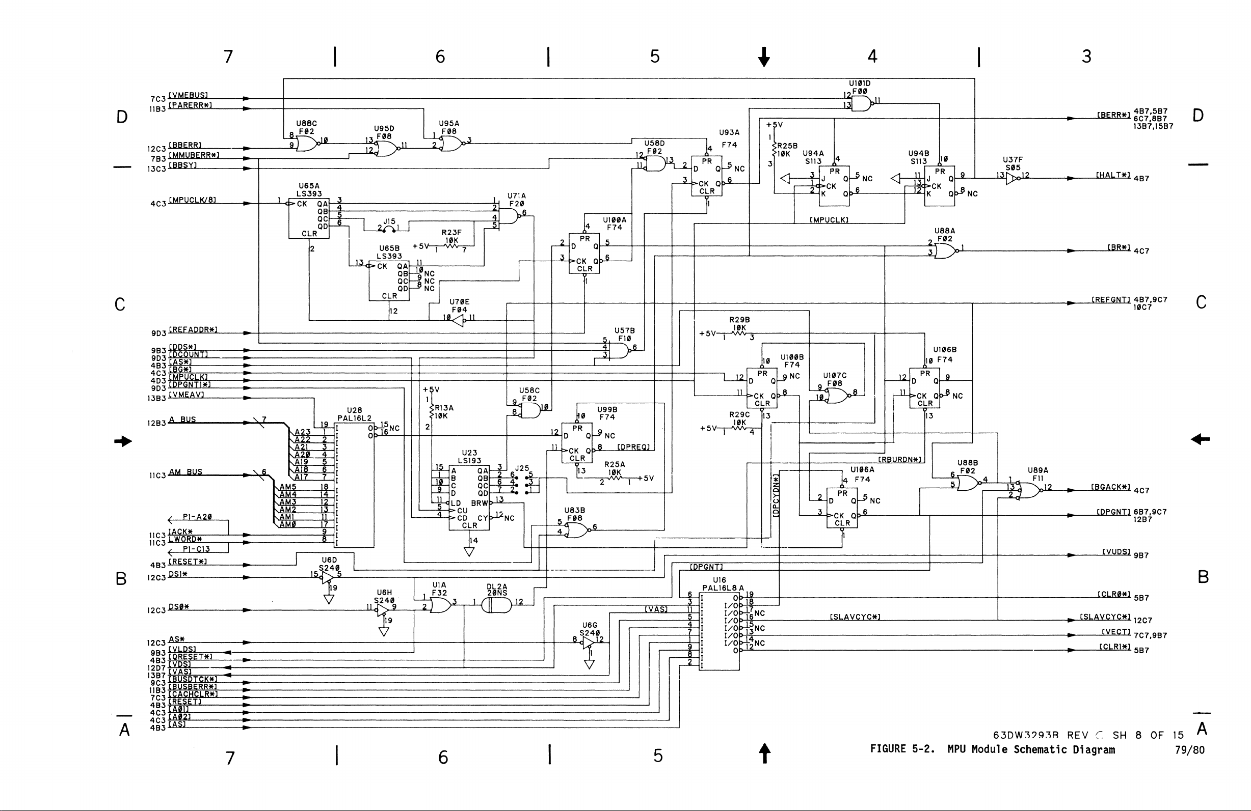
Artisan Technology Group - Quality Instrumentation ... Guaranteed | (888) 88-SOURCE | www.artisantg.com
Page 81

12C3 [OPCOONE*l
o
II
13C3[PU
c
..
13C3
B
7
B3 [UP
A8""E.L!.R'-'-'Rl'---
8C3~.9~-----
Al
6B3
[BOROl
B83
WPGNTl
4D3
[MPUCLK*l
403[MPUCL~-----.--------------+_------_-~----_rI------+-------l---I---------L----+-------j--+_-+------I
t,H:A~,~~~--~--------~~4~-<FI1
4B3[R/W*l
4B3
---
CPU
Cl
4B3ID~Sl--------~~--~------------------+_-------'1~2D
6B3
CPU
Bl
___
~---
..
_.
_______________________________
••
-------------------------------~2YD
- 31
U70F
F04
5 \ 6
~
+ 5 v---:-
U89B
.J}-,<--+-+---+--'-"'-fD
+sV'----j---.~~s~~1
'--
6
r-
_________________________________________________________
,---
______________________________
R25C
10K
4+-
_______
4
,..---"--,
PRQ~
~~CK
1--~_-_-_-_1_I----------------1_I-_j+--+r---++----------------~--------+_---L.---1f--1'
.~
I"
11
R2SE
10K
-'V\1\r-:
I
12
-----1Lp>CK
Qb-' 6"--
CLR
I
'___
____
+
;iV
I
R25D
10K
PR
0
Qr-JI
CK
Qb-8"---+--'--_~2'_Q
CLR
13
:---i
6
10
~~
PR
I 0
Qi->'
Q'
CLR
']13
R230
10K
10
.---:~-,
PRQf-~9__j~
__
K Qt:>-8,,---+-----,
-<J-'--?J
C
CLR
13
-++-+-
UBIA
F74
NC
__
-+--1
-j-++
UBI
B
.-+-+----'"-<~:L.-/
F74
NC
__________
+ V
I U33B
RI4B
IK
3
r---~ll'-?-CK
________________
~
2]
L---';
tL3..!'Ot-_
12
U66A I U45C
)J
,~
US7A
F
,1
0 P R
)12-11
11
_.LL
U93B
F74
NC
8 5 F00'\..6
~~
U101B
r-
I -
r--
__________
U72B
F74
AI
~~A~---~___ll
~~,*--------*--jI
1A-=~:t;L--------~1
~'?_!'_!~---___x____ll
'~LO..Oo.XL----~-=--=--=-tj1
I--
10
(')
PR
O~
Qb-.'L-B---,
CLR
13
[RAS]
F32
10
10
0 Qf->L-
>CK
CLR
13
5
____
-+
__________________
F74
NC
.-_--"2
-r
____
}ll..B-+----+---+------.
U43B
F74
9
--l
8
OP-"'----f---l
'---+
-
U4S0
13.JE
~12~~_
U31
PALl6L8B
I 0
1/0b-+,~--+_----------------+--'
I/OP-+!!----+--------."')=K*----------'
I/Ob--!-l~--+--------''-'''-'-'~-------.,
I
/O~~--+-----;-;-;V"':A
1
I/O
I/g~
9NC~
PR
"
y
LI
~
>CK
CLR
r---'
~---+_--f___f___-W~/~M~MU]
W/MMUI JI4 ~ 0 Qf-><--S-+-+-r+.J..
__________________
.
______________________
UI070
1
U99A
4
F74
Qf-"-S.-+-+-+---
+_....11~3-F0~\
u
1-'-'-------,
______
O~
Y,
--.-----1--1----------,1:,.
I 12.5 3
+ V
I
RI2C
~
2200
L---,--
____
-+-+--+
U36A I
F74
____
-+-+--1-'-+-
I 2. S
2')
3
4
4
'---:P~R::---1
3
CKQ:r2--
CLR
I
'---
-+-+1-
U70C U70A
6
F04
5 2
~---<
F04
I
b-~-+-+-+-------------------'
r+
I
...
S",-;;E=-:N;-::-*-------;----,I
U"IC
4
--,
JIB
2
"'-1-+---']
...
'-
____
11"'-120
Il-P>CKO,8
____
+ S v-----'-I -'\AI
__________
+9
IPs
W/MMU
____
+ 5
V'---7""1
+ S V'--;---"I",I K'Ir-.
1-
_____________________________
-+-
______________________________
Q 6
----'
-,
5
__
__
-+
A
____
-+
____
RI8A
4 7
2 I
RI8C
41
4 UFB/4
~L--,
---'-.1
PR
0 Q
3
CK
CLR
---,
~0
P R F 7 4
CLR
-"-<I3
I 4
U368
Of->L-9-----+--,..J..
l3
~~~~
2 I 5 V
----"'-
__
RI4E
KfIr--=---,
6
_-L-l
U70B
F04
4
RI4A
IK
--'\IV'\r-;:2---'
RI4C
__
UIBC
9 S3B
~
l'...a
~
U4SB
4
F32
..5..J
)p-"'--
10
l2.. D
PR
Q~
111
Y>CK
Q'
CLR
13
-+
_______________
-+----,;---Aw41\171r--;;-
6
____
U878
F74
8
R
18
8
3 4
1
_____
3
.
.--~GNTI*lBC7
.lli.E£8~
BC7,I007
o
PI-AI6
)
OTIl,CK*
[BUSOTCK*l
--l_--"W-"'-""C: I
IIC7
BB7,I207
O"-,LU,,,-,-JIN n BC
7 ,1007
c
WPRI60*l
[RASI60]
Jru!LQl
----
----'[u;:Ru::lA\~Si*~
(RAMROD
[RAMGOl
[UCAS*l
~
[lCA
WOS*l
..
IIB7
8C7,I1B7
687
10B
7,1207
6C7
6C7,I187
8C7
1087
1
1'.'
,I0C 7
B
A
1D3:::~:::E.,
I
~g5
~[L'I_!!0~S;;*+l
4B3~[U~0~S~*+]------_.-------------------------------------_f__--------------~
8B3~p~A~SCO~Sl*~l,---··---------------------------------------f----------------~
6B3~V~D~S:~~--
8B7~lN~O~G~O~*~]------·.--------------------------------------_f__------------------------------
7B3
8B3
7B3
7C3
______
[YUOS] -'>l.,
(VECTl
(IAORHIT*]
[MAS*]
.....
:---=------------=------------------------------------------=----~-----------=------------=--.-----1_---------------------_-_~__.J
.....
•
___
.--
7
':?
------------------------------------------f-------------------''----------
_______________________________
6
Artisan Technology Group - Quality Instrumentation ... Guaranteed | (888) 88-SOURCE | www.artisantg.com
...1-
_________________________________
---;:::::1
U191.
4
~
~J. 6 ~
~
U20C I
~S146
5
'-"
VV"
5
~~_~~
>
----------+-------~I
J
rUSSO
_~
8
I V
---'
t
r-------I.~--U-7-1-B-+--s---6------------f---..L-[~,IJC7
L
~20
1'-
,,8
1111
.r-
9
(MASl
12B7
1~.
81/82
A
FIGURE
5-2.
MPU
63DW
Module
32938
Schematic
REV 8
Diagram
SH
9 OF
Page 82

D
c
7 6 5
903'BS9~~UN~IT~l.---~--------------------------------------------------
903
Lrct:.r:AODR*
483[Al
7D3
9C3
8C3
l1B3
BUS
[TAl
BUS
[R*/C)
[REFGNTl
[WHPAR]
64K
256K
J23
rP
3
I
" 9
[A09]
[TAI71
" 4
I'
" 5
I'
,[A0ll
" 5
, 5
[R3]
, 4 "
"
,[A
15J
[~
IS)
:A
17
l't'A~6~]--t,+4~3A
,['
'A
~[T~A~,*l
1~....,A~If-~rl28
I ,!,:!:,:,
--~18
A~~-+!--f
1'-
2
5.
IA
2A
4A
38
48
SEL
U51
F257
" 4
IY
2Y 9 [RST
3Y
4 Y
OEP-U<-
U53
2
F257
IY
4 [Rial
2Y (R
9 :R2:
3Y
12
4 Y
f-'-'''---''-!.l.>t..<,1
______________________________
4
[R4]
7
[R5]
12
[R7
f-'-'''--~u....1
I
,,,
RI28
22"0
3
,[A09]
1----i,~2A
,[TAI6]
~~~-4--~~IB
~--:~c:-t3A
~---'~4A
~----:i,'!:--f
1-~,~3B
'----'-!'Y4B
II--L.~S~EL=---~O~E~
~
F257
IA
28
U50
lY
2Yt&
3Y 2 NC
4Y
4
R208
-,
U56
PALl6R8
r--!
c-
I
r-';-
4
NC
NC
L
15
I--:
'-
---l;-
---i;-
-,..--1
---If-I
--::-1
I
I
I
1
OE
" 8
19
[R0l
[R8J
47
3 4
R20C
47
6 5
R20E
47
10
R200
47
7 8
R19C
47
7 8
R20A
47
I 2
RI98
47
3
9
4
[RA0l
[RAlJ
~RA21
[RA3]
[RA5l
[RA
7]
[RA8J
3
D
c
..
983
I1C3
B
12C3
9C3
9C3
(UCAS*l
[WLPAR]
[RW*]
lRAS*
:AS*
" 8
~
" 9
"
!J 5
1~~~---7~A0
1~~~--~,4A3
1~~=~--~4A4
1~~~--~~A5
1~~~--~~A6
I
,*,~:'!-+---4--f
12
6
1"\JoJ.).O.!,U-.f.-,--4--..l.......l_~6
I
rW
" 9
"
~I
1~~:A~--t-+-'!!!-1A0
I~~:~~~-+-HAI
~~~~~~=~~~1~2~A2
I'
l~r~~~HI~0A4
1~~~-H~:54A5
r+!~~~f-19~A6
1'!!.~;t--~I-+~A7
5
1
3
4
~
e
r.:--
12
14
01
DO
Al
A 2
A 7
m
~
~
r.:;---
12
14 MCM6256
01
DO
A3
A8
L
Ws
U61
MCM6256
B]
~~~-*7~A0
] 6 Al
~~"----;';;:-i
~~~~~A3
~~~~I~A4
~R~A*]~~I~A5
:RA A6
H:&~tA"'='*ll!---+--11A
IRW*J
i~~~;*l
U62 r::;-- U69 r.:;--
[RA J 5
:RJ
:R,
R
Ie
7 9 A6
IB A7 RA8: I A7 [RA8 A7
,...[=RW,*
.....
fJ--'-13A8
:RAS*
:AS*
r.:--
12
5
01
A 2
7
3
~6
11
m
~
~
12
01
7 A0 [RA 7
6 AI lRA2: 6 AI
12
1 A3
10
13
4 L
15
DO
A2 RA3J
A4
A5
ffi
U68
14 MCM6256
f4
MCM6256
[RAIJ
tA4
tA5:
tA6:1J.
tA
7 9 A6
(RW*]
lRAS*
:AS*
5
12
10
3
4
15
r.:--
12
12
01
A0
A2
A3
A4
A5
~B
fu
CAS
U74
14
MCM6256
DO
tA0]
tA
~t~A:------!:-6--fAl
~t~
A"----;>;;2-1 A 2 1 A 2 1 A 2
f*t~A~~'~
~t~A!---H.~--f_A4
w.lR~Af--~HA5
Hl~
Rt~,
A7
!--l;?:'rl
~~~:~JA8~~~-1A7
I
[RW*J
~[-!H'R,A-i:S,*:L.:----'!'-4-1L
~~~,:H
[
CAS*
~
~
U75
14
MCM6256
DO ( tA
tA
tA
tA.;
tA
~t~A~'1~0A4
tAl3
RA
7 9
[RW*]:5
lRAS*
:AS*
5
3
15
5
7
6
12
4 L
15
~
o
~
r::;-- U 7 9 r.:;-- U
f_. 4 MCM6256
01
DO
A"
A3
A 6 7 A 6 A 6
A6
BAS.
CAS U
r::;-- UBt' r.:;-- UB6
12
01
A0
Al
A2
A3
A5
A6
AB
R n
~%~-*~A0
[RW*J
.tR~*1
~
~
14 MCM6256
DO
~A';"!"~J_~~
~!~A';---k-rlA0
!A2: AI :A 6
~"?A~3!---:,~A2
~7l'*"4--'~A3
~~.~5:-.~A4
t1~~l~B:~=j,~=:A5
r.
~~l*8:--+1rlA7
[RW*]
~
~
\~
3
_~
AS*
5 CAS
7 A6
j-
Hl~R~-¥,AI~:S,*t..-74rlfu
Ws
.CAS*
15
~
~
~
l~
14
Dl
DO
AI 6
A3
A4
A5
A7
A8
L
BAS.
!
e
12
,14
01
DO
~8
CAS
65
MCM6256
RA
11)
tA
tA
'[RW*J
,lRAS.*]4
UCAS*
MCM6256
:RA 5
RA
:A
:A 1
:A
tAe
RA
:RA
tRW*]
:RAS*
:AS*1J5
J'
I
15
12
10
13
~
3
7
9
I
3
4
A0
Al
A3
A4
A5
A7
A6
L
BAS.
CAS
A"
Al
A2
A3
A4
A5
A6
A7
A8
L
~
CAS
~
~
~
r::;-- U
12
..
14 MCM6256
01
DO
tAl]
:A A0
~:~A~---J,---16A
tA
w.lt~Af--~'--j
~:J?-i!-A!--~IH:--f
~:~A~-i,~A5
~:~A!--l;?:'rl
~:~A~~-lA7
fAU~'----'--l
I
[RW*J
llRAS*J
UCAS*
r.:;-- U92
12
14
MCM6256
01
DO
:A01 5
1-*:!:~Af---*--I7
~:~A.---*-I6AI
~:~A~)
~:~A~~,~A3
w.lR~Af--,H.0rl
~[~R:"?,A\~€~~3-lA5
H[~R:~JA!--~'-i
H[~R:~JA~~~A7
I
[RW*J
w.lR~AI~Si*'--"'14~~
:AS*
91
----,,~2c-1A2
r::;-- U 9 7 r.:;--
'4
e.
:
01
1
I
A2
A3
A 4
A 6
A 8
3
4 L
BAS.
15
CAS
r:;-- U98 r::;--
12
OJ
A"
A4
A6 7 9 A6
3 AB
15
CAS
MCM6256L.
DO
~"R'<'----*rl
~RJ?-i!-A:!--~IH:~-1
[RA
[RA' 9 A6
[RAE
(RW*]
[RAS*]
'*'U~:7
14
MCM6256
DO
[RA! 5
[R
A 7
eRA
RA
lB: I A7
tRW*J
RAS*
.CAS*
~
~
~
U103
MCM6256
14
:A
IJ
5
n 5
AI;:CSi*~,c::rl5
01
A"
6
Al
2
A2
1 A3
A 4
13
A5
J A7
3
~8
4 YL-
Ws
DO
tA 7
tA 6 Al
tA,
tA' 1 A3
R
[R,
~l~R,±7!--~--fA
f-"[,,-,=RJI.><.6::
[RW*J
eRAS* 4
U
:AS*
r-:'-:01~0:"-:0-'
12
~.
J 3
1'----'-'4
3
15
"
16
"
UI04
14
MCM6256
[
JJ
~~;---k--lA
~~~-;,~A2
~~"--~,
~r::iff-~IH.-lA
~~~""'1f.!3'-~A5
~~7~~9'-iA6
Hr~\*8---'f-,
[RW*J
lRAS*
.CAS*
r-'---'--,
~
~A3
-lA
3
4 L
15
6
12
10
13
3
4
15
I
12
01
DO
A"
Al
A2
A3
A4
A5
~8
fu
CAS
2 14
A"
A2
A4
A5
A6
"
A 8
iii
W.
CAS
2
01
A"
1
4
7
AB
BAS.
CAS
14
DO
[RHPAR] 1187
Ul"9
MCM6256
[0]
BUS
tRLPARl
UII0
MCM6256
4C3
1187
B
A
7
6
Artisan Technology Group - Quality Instrumentation ... Guaranteed | (888) 88-SOURCE | www.artisantg.com
5
t
FIGURE
5-2.
MPU
63DW32938
Module
REV 8
Schematic
SH
Diagram
10
OF
i~
83/84
A
Page 83

D
c
..
B
A
9831.YECT
1583
70J
4B3
13B3
4C3
7B3
10B3
I"C3
9B3
12C3
7B3
9C3
403
12C3
9C3
403
13C3
*1
.U·\c.l<~L
lTh1..JEi
w;,1
BUS
[VMEAV*]
.....
~,
ill
I3!,JS
[WW~*l
[RLPAR]
[RHPAR]
[RAMGC
[RAMWRTE*l
(P8RJ;;N*]
(RASIS"]
(RC]
(DPC~ONJ;;*l
~~~RI6!1!*l
(MPUCI.KJ
CPU
A]
7
______
~
~
, .
....
--.--
~
~
~
~
~
~
~
------------------.
'\.8
"
'\.
3
\
".
U2"8
3~\
V"
U37C
~S6
.
+SV
I
S
TAIS]
·AI7]
·A
TAl
[TA2"]
TA2
TA22]
TA23]
RI2E
22""
8]
9]
UISO
1i-~8
131
1)11
UISC
1fl)
9
.8
~
6
3
U38
2
I
~"8
11
c----/
~
S
5
+
~V
I
RI0C
4700
4
+
~V
I
RII8
47"0
3
'\
000]
D"ll
8
I'
+ v
R23A
I"K
2
102]
03
04
105:
'06]
07]
)"8]
HI9:
10]
I
1
I
1
S
U2"0
LSI4
9~8
I
I
4
12
4
I
2
"
I
3
1
2
!'-
0
I
2
3
,...----
J24
~I
+5V
UI3
F280
ODD
EVEN
UI4
F280
ODD
EVEN
-"
..
...
1·-
-
U4SA
F32
.r.-,::,,::,
I
2]
RIC
I"K
4
.--
_.
~
~i
+5V
H
5
_.
U42A
F"8
2
.J
~
5
--~.\r------·
~(~C~3--·
R21E
~
+
---
5V~--
I S
10K
-
-
----.-J
r
R21F
10K
I
US88
6,£.!2
U2S0
[FC2.l I
[
C!l....
~:
7
U4SC
9-.
l.ad
2
I
Q.2
J13
ON
PARITY
.4
J
-
:OLL
OL2C
20NS
15
6~
--+
__
'\.
8
EN
U4S8
5~
----/
+5V~4
II
17
I
I
\..6
UI9
S24't
[>
2 0
3
t2
n
R21C
10K
E
E
CK
CLR
0
CK
CLR
9
16
18
3
14
5..
2
19
14
PR
a S
a
r 3 5 8
b"
PR
a 9 4l
a
3
r
U64A
F74
c6
U648
F74
.8
4
AMS
AM3
AM4
AM
AMI
AM"
+5V
2'
2IO
:iT
10K
I 5
'§..
--
U18A
2~
3
ILl)
63DWj2938
3
----.-.
_------!M..Q.lli
·
.....
--~~----'~
--.~
__
..-lY-Mf:VECT*]
PI-CI~
1
~J
~
~._
-
.-
LWORO*
PI-A23
PI-B18
P
PI-BIS
.-~
-
~.
""",,----AM.
[
~"ill.
IACK*
-B17
~
IS07
ISC7
IS07
707
8B7
887
887
D
c
[WI.P';Bl
I
~
~U~8RJ;;RBj
~-
[WHPARl
~
[PARERR*]
~
[PARERRl
U.!Ul:!8~RR*l
~
PI-CII
REV
8 SH
BERR*
10C3
907
1"83
807
407,IS07
887
"-
/
12C7
11
OF 15 A
B
7
6
Artisan Technology Group - Quality Instrumentation ... Guaranteed | (888) 88-SOURCE | www.artisantg.com
5
t
FIGURE
5-2.
MPU
Module
Schematic
Diagram
85/86
Page 84

Artisan Technology Group - Quality Instrumentation ... Guaranteed | (888) 88-SOURCE | www.artisantg.com
Page 85
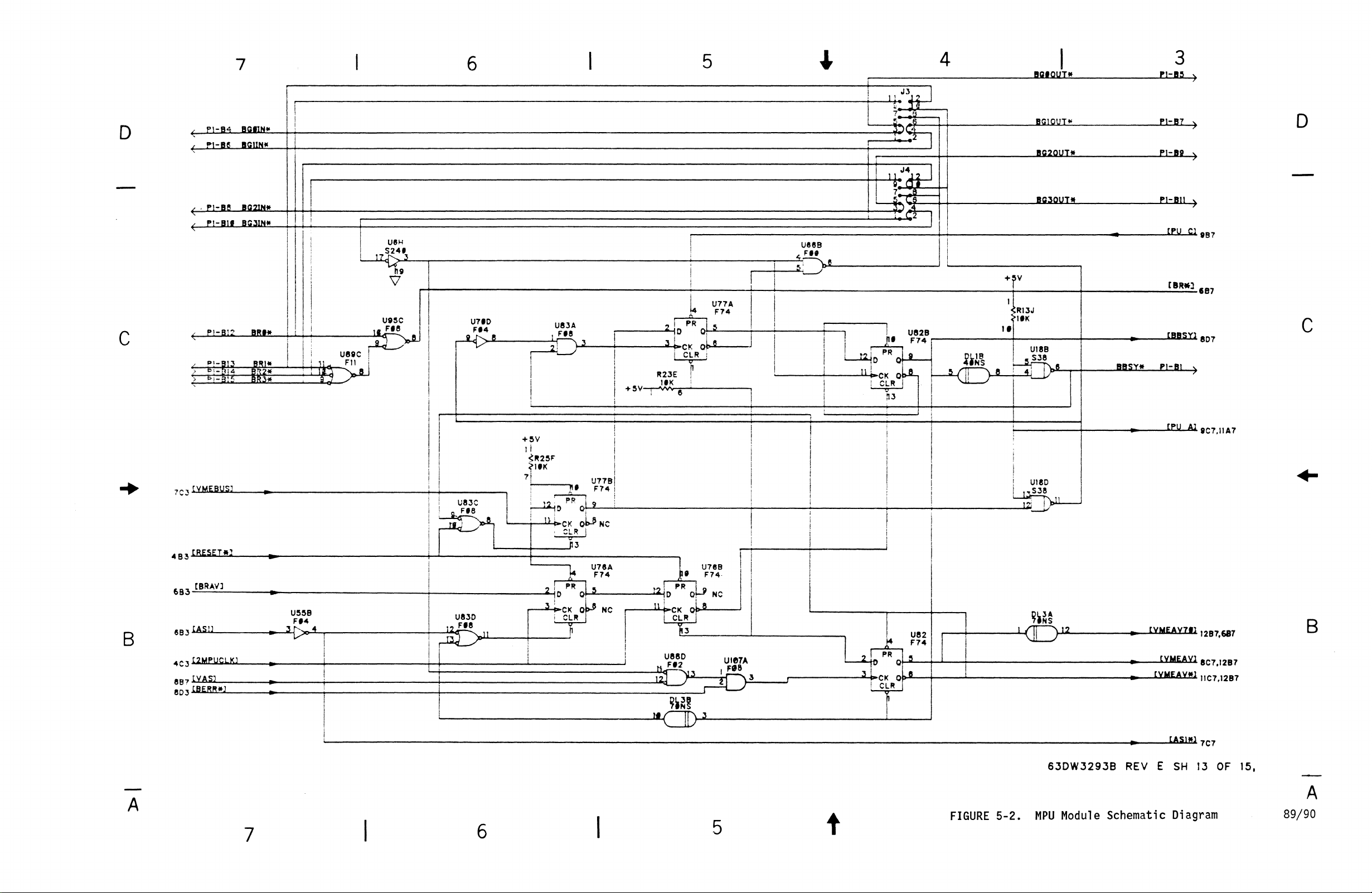
D
c
7
r-
________________________________________________________________
!'l-RA
"'
!>1-1I11
./
,PI-AI!
"-
PI-BI'
~I-BI'"
<i--I~
~~j:I~li
ACl.-tN"
IIGlINII
IICl?TN.
BG:]IN.
1111_.
~t~+;-~:
I
II
I
I
I
I,
I
I
I
i
i '
I
----.....!
i
~I1D-J
I
uaec
UIIH
S24_~
hi
V
uasc
I.
FIe
LJ~
I
I
I
I
!
6
uno
F.4
rv
5
~~J!(J~
7
••
,
• "8
I'~
I
I 11
J4fi]
I
~
~
>
"~2~
I
!
I
,
,
L
U71A
'
F74
U83A
I
e
FIe
n
3
+5V~~e~-------.
2~5
!O
Q,
I '
J
'"
CI<
ob
i
C'~R
I
R2JE r
11K
e
I
i
I
J
,
<,FIt
i
I
I
!
I
______
UIIIIB
5D"
-'-
__
I
,
I
~o
!
nl
~
PR
...L1
~I
~IOo-CK
RI
lCb
~3
o~
o~
4
IlIi'OUn.
'.J
I
I
IIGlotlT"
IIC?OIlT*
~
IIC:50UT*
I
!
I
+fV
'1R13J
ua2B
F74
I
~ . ~
,
£.~\
~JTi'f-'e,,--_'
~'
I
,
I·Ilfl(
8
I",>,
c;
U
B I
'
s
3
e
...-.;
--:L{J)p:e5l..-r-1+
I
..
I
I
__
•
..JBUiBLilS~X*!!.__'fEJ!.::..-
3
rJ-II~
)
PI-In
PI-II11
PI-1I11
tPu
Cl
[DR*)
[BIISYl
B;uly),
o
ee?
IS7
c
807
---------'---_1
!------l---_--..IJ::.!.
[P·UL...&
All
eC7.11 A 7
..
B
A
7C3
..
683
83
rYMEBUSJ
tRESEHtl
[BRAV)
7
...
I j
:
va3e
~
LI
6
5
t
FIGURE
5-2.
63DW3293B
MPU
Module
•
tYMEAY7'1
• tYMEAYI
• tYMEAY*1 ItC7.12B7
•
REV E
Schematic
[AS!*l7C7
SH
Diagram
1287,687
eC7,12B?
13
OF
B
15,
A
89/90
Artisan Technology Group - Quality Instrumentation ... Guaranteed | (888) 88-SOURCE | www.artisantg.com
Page 86

7
6
5
4
I
3
D
c
B
4B3[A1
703
fT
A1
BUS
BUS
, Q
'--
"
D
7
, 3
t--
, 2
f'.
,[T
A 13]
~~~=uAI6~:J
______
~?
fTA14J
~.4t=-=-~~",u.:u_-/]
~
+5V
~_"""\:,~~!:--_1-,,-'T.1..j-'i-Pr!'~~ITf-:J
4-~r
6 V
7 ·AI5:
.~6
____
-+---"
-+
___
~~
(P271
(P261
(PIJ
r-+-------h........,=-------~
[P201
[P23J
+ V
r---r--~-~--~-~--~
1 1 1 1 I 1 1 1
RIH
RIF r,10 <
10K 10K
7
9
:
Ci
~
~
;:;;:;
~--~----~--~----~--~----~--~~--,
+!V
1 1 1
R15E
15K 15K
8 9
"RI5G
5 2
~
~
&
C
;::
RIA
RIJ
10K 10K 10K 10K 10K
R15H
15K 15K
10
~ ~
8 &
e;::;:;
1 1 1 1 1
R15F
?R150
7
5
::
e
RIG
8 6
:0
~ ~ ~
)oR15A
15K 15K 15K
2
;;:,
c
;::
..
---
R1E
< RIB
10K
CD;:;:
_ [A
'---_-'[
, 8
[Pll
.... P
....
2L......J
f'
'>RI5B
R15e
15K
,
18
___
, 8
t--
XU52
1 SOCKET
~[~
AI~6:J!__-----_'!!3~
~~A~7~Jf__-----..:;J:4~
~A~6J!__-----~A6
:A
15J
~:~AI~4-----~~A4
~A*0~3J~-----~A3
~:~
A0'~2J!---------'!!--l
~A~~ll~-------~Al
"""''''"*0-=00.--:-----l:¥-l
r.'(~[D~0~ll..__---____lI~
'8
-+
02
'"
"
......
=c--
_____
'8:
~[~AI~7J~-----~A7
~~~.~6J!-------~A6
"[""A~5"'J
-----~f--<
~~(~A~~-----~A4
,"[~A~J-----~~A3
~~(~A~-----~9~A2
[A0
J
"[;;;:)~
0fJ...--------¥.'-1
/,[~0*9f-J
---------+2:!:-1011
'[0101
1~~L------~~02
"'
16
2 VPP VCCf-! 7 P 7
A
12
PGM:~[§:-l:-------l!l=P~~--+--I
A 7
A5
A2
A0
00 06
01
~~~G~N~0~~0~3r~II~~--~~0~01~3-t-t-t-r-t--t/1
02
XU44
SOCKET
~vpP
10
13
14
VCC~
A
12
PG
A 5 A
Al
A0
01
GNO
+ V
NC~17-5------l;';;A~~-----1
A8·~¥4---~"A~f----+-~4-~
A9~.,;_--""'!O_:!_:!iP"l-!-~--+--~1
"A
, 3
P?
)06
)05
'041
[P27J
'A
P20
9
07
18
17
05
16
04
+5V
7
MH<'7<------J[;-!.P~216Jf--+-+-4--l
NC~~------l[~AI0~9!--+-~
A81~~--~~·A~I~0~-+--~f--J
91H::.;;------"-;~P~2L¥f-3J
2
!0
19
07
18
06
D5
.u.
04
~
03
15
0'
07
--+-+--..../1
, 1
f'.
, 2
"
, 2 , "
f'.
('DI5J
[
14J
013
(1112J
[0111
f'.
f'.
16
,
18
[m
RUe::
4C3
"'
c
B
'-
A
7C3
[ROMEN*J
7
6
Artisan Technology Group - Quality Instrumentation ... Guaranteed | (888) 88-SOURCE | www.artisantg.com
5
t
FIGURE
5-2.
MPU
63DW32938
Module
Schematic
REV 8
Diagram
SH
14
OF
1~
A
91/92
Page 87

Artisan Technology Group - Quality Instrumentation ... Guaranteed | (888) 88-SOURCE | www.artisantg.com
Page 88

@MOTOROLA
APPENDIX
A
RS-232C
The
computers or
the
conform
Many
art
The
terminals via
many
RS-232C
lines
for
standard
modems,
are not
their
is
the
and
yet
clearly
applications.
times designers think only of
is
computer-to-computer or
RS-232C
standard
modems.
was
originally
Therefore, several handshaking
applications these are not needed, but since they permit diagnosis of
problems, they are included in
Table 1
this
information
lists
the standard
correctly
it
connect a terminal to a
without
Because
said
and
Any
and
modems,
one
must
be
configured
computers are normally configured to
to
be
configured
+15
volts
for a high
attempt to connect
is
not allowed
as a modem.
units
by
the
level,
RS-232C
APPENDIX
A
INTERCONNECTIONS
most
widely
it
is
not
defined,
used
fully
and
A system should
their
own
computer-to-modem
developed
many
RS-232C
is
modem.
applications.
interconnections.
necessary to
When
computers are connected to computers
as
a terminal
Also, the signal
and
between
in
parallel
may
specification.
interface
between
understood. This
many
users
easily
do
not see the
connect to
equipment, but the
operation.
by
the Bell
know
-3
and
result
that
work
-15
lines
and
with terminals, they are
levels
in out of range voltages
were
In
order to
RS-232C
the other
must
volts
terminals
is
because
state-of-the-
System
included.
is
intended to
as a modem.
be
for a
and
all
need
any
to
other.
to connect
In
interpret
between
low
+3
level.
TABLE
=============================================================================
PIN
NUMBER
=========================~=========:==================
1
2
3
SIGNAL
MNEMONIC
TxD
RxD
1.
RS-232C
Not
used.
TRANSMIT
on
this
RECEIVE
receive
DATA -Data
line
DATA
line
Interconnections
SIGNAL
NAME
AND
to
to the
modem
-
Data
that
presented to the terminal
is
DESCRIPTION
=======================
be
transmitted
from
the terminal.
is
demodulated
is
modem.
4
RTS
REQUEST
to the
With
RTS
RTS
is
turned
TO
SEND -RTS
modem
off,
on,
when
the
the
is
supplied
by
the terminal
required to transmit a message.
modem
carrier
modem
remains
immediately turns
carrier.
furnished
from
the
by
the
off.
When
on
the
95
Artisan Technology Group - Quality Instrumentation ... Guaranteed | (888) 88-SOURCE | www.artisantg.com
MICROSYSTEMS
Page 89

®MOTOFlOLA
APPENDIX
A
I
TABLE
1.
RS-232C
Interconnections (cont'd)
=============================================================================
PIN
NUMBER
SIGNAL
MNEMONIC
SIGNAL
NAME
AND
DESCRIPTION
=============================================================================
5
6
7
8
9-14
CTS
DSR
SIG-GND
DCD
CLEAR
terminal
permissible to
When
transition
DATA
modem
ready to transmit data.
SIGNAL
at
DATA
terminal to indicate
received.
Not
TO
SEND -CTS
by
the
using a
of
RTS
SET
READY -DSR
to the terminal
GROUND -Common
the
modem
CARRIER
used.
interface.
DETECT
is
modem
begin
modem,
after a time
transmission of a
CTS
is
to
- Sent
that
a function supplied to the
that
a function supplied
indicate
return
indicates
follows the off-to-on
delay.
that
line
by
the
a valid
carrier
for
that
message.
the
modem
all
signals
modem
is
it
by
to the
being
is
the
is
15
16
17
18,19
20
21
22
23
24
TxC
RxC
DTR
RI
TxC
TRANSMIT
modem
the
Not
used.
RECEIVE
terminal to a
Not
used.
DATA
TERMINAL
the
modem
send
or receive data.
Not
used.
RING
terminal. This
an
incoming
modem
the
while
Not
used.
TRANSMIT
CLOCK
from
the terminal.
CLOCK
modem.
READY
indicating
INDICATOR
call
to
RI.
CLOCK -Same
- This
- This
- A signal
line
is
answer
line
line
that
RI
is
indicates to the terminal that
present.
the
as
TxC
clocks output data to
clocks input data
from
the terminal
sent
phone
on
the terminal to
is
by
the
modem
The
terminal causes
by
carrying
pin 15.
from
ready to
to the
DTR
true
a
96
Artisan Technology Group - Quality Instrumentation ... Guaranteed | (888) 88-SOURCE | www.artisantg.com
MICROS YSTEMS
Page 90

®MOTOROLA
APPENDIX
A
TABLE
==============~=======================================
PIN
NUMBER
=============================================================================
25
=============================================================================
NOTES:
=============================================================================
There are several
RS-232C
and
automatic
middle-of-the-road approach
1.
2.
interconnections.
a ground.
SIGNAL
MNEMONIC
BSY
High
dialing,
level =
RS-232C
computers are connected to computers without
computers
terminal.
The
1.
RS-232C
BUSY
causes the
associated
+3
to
is
intended to connect a terminal to a
must
levels
full
automatic answering,
be
of conformance
The
version of
is
Interconnections (cont'd)
SIGNAL
A
phone
+15
volts.
configured
bare
minimum
RS-232C
illustrated
NAME
positive
modem
to
busy.
Low
as
that
requirement
requires
and
in Figure 1.
=======================
AND
DESCRIPTION
EIA
signal applied
go
off-hook
level =
a
synchronous transmission. A
-3
to
-15
modems,
modem
are appropriate for typical
12
and
is
lines
the
to
and
volts.
modem.
the other
two
and
accommpdates
this
make
one
data
pin
the
When
of the
as
lines
I
a
One
set
of handshaking signals frequently
used
modem
microseconds.
202
to
usually necessary to
of
jumpered to
for
purpose of
distant
software
diagnose
properly
must
Figure 1).
signals are
of
in preparation for another automatic
signals to
a
signals are not received
the
connector
with only
in
many
application,
modem
avoid buffer overflow. This
+12
this
be
trouble.
good
needed
systems to
RTS
(half
volts
purpose). Another signal
modem
to
failure
to
provided
used
talk
minimum
can
three
duplex).
such
an
MC1488
this
signal
signal
was
display a
to
use
Many
The
this
by
OTR
to
configuration
be
wires. This
inhibit
RTS
is
as
being received. This signal
by
modems
software to help
all
artificially.
wired to enable a computer to connect
is
turned around
programmable
CTS
is
make
the
gate
communicate.
signal
CTS
resistors
that
was
to
message
signal,
a pullup
expect a
is
possible
from
is
transmission until the signal
in
used
is
high
has
used
tell
like
and
it
resistor
used
modems
that
the
modem,
because
implemented
and
some
systems to
in
some
systems to provide flow control
not possible
by
connecting
shown
its
the system
Obviously,
prompt
sometimes
almost
Figure 2
in Figure 1.
inputs grounded (the gate
in
many
CARRIER
is
not connected to a
DTR
high signal
the operator
call.
(see Figure 1).
the jumpers
most
systems
that
NOT
or gate
to disconnect the
It
is
always
shows
terminals
are
returned
work
if
modems
it
to
the
is
frequently
PRESENT
if
the system
as
and
necessary
works.
can
a
have a DTR
RTS
and
CTS.
is
high.
as
CTS
with the older type
are used.
RTS
or to
It
is
is
DCD.
carrier
to help the user to
modem,
described before (see
issue a
as
to
to
As
shown,
If
be
moved
way
to
a basic terminal
some
also frequently
is
The
tone
used
is
DSR.
possible causes
phone
provide these
Figure 1
the
CTS
that
signal
CTS
is
In
the
after
provided
original
from
designed
the signal
to
an
150
It
is
source
the
by
the
These
circuit
is
and
OCD
provide
RS-232C
that
97
Artisan Technology Group - Quality Instrumentation ... Guaranteed | (888) 88-SOURCE | www.artisantg.com
MICROSYSTEMS
Page 91

I
®MOTOROLA
is
ON,
and
that
can
be
used
to pullup the
these connectors wired back-to-back
the handshaking
occur.
terminal
Also
is
outgoing but the
the
has
Tx
been
and
bypassed
Rx
Tx
line
can
and
lines
on a modem
be
CTS,
used.
DCD,
It
must
and
DSR
signals.
be
realized
possible diagnostic messages
may
have
is
to
be
crossed since
an
incoming
signal.
APPENDIX
Two
that
do
Tx
all
not
from
A
of
a
RXDr-------~-------~---__a
RTS
---------,
CTS
1-------,
DCO~----;'
TXC~---,
RXCf----
6850
TXDI------l------------~
RXDI-----~
RTS
CTS
DCDI-----.
.....
r------,
1------.,
I I
I :
I I LS08 I
I
L-(""--,
: I
t----L_j
I CPTIONAL I I
I
I TRANSPARENT I I
I MODE I I
I I
I LS08 I
L
___
r----t..--/
I I
I I
I I
I I
I I
.
12V-'V\N---.J
~
+12V
~---,
I I
HARDWARE I I
-(""--,
I
39kll
..
...
I
I----t----...J
I
I
I
I
I
I
I
I
I
L
______
,..---,
LOGIC
I - I
.,2V--'Y39"'kl,-I-.....J
,'2V
__
I
I
II
GND--+~"'I
"2V
~l..-4_70_1l
_
-_+_---.,
47011 47011 47011
CTS
DSR
'------I--~
DCD
SIG
G'.o
L CHASSIS GND
·-+------r...=.::=:....=:.:=--Tb-,
. SIG
G'.o
6
< 7
____
~D=-~
__
~~~:~~.:~
~O
RS·232C
CONNECTOR
TO
TERMINAL
(DTE)
RS·232C
CONNECTO
TO
MODEM
OR
EXORciser
OR
EXORmacs
(DCE)
I
I
::~b
'----~~l=:!J~--~~--L--.....c<58J
-12V~
~
~DULE
_______________
FIGURE
Another subject
are
the
it
two
distant
must
pins labeled
device to complete the
be
used
1.
Middle-of-the-Road
that
needs
GND.
with care.
through the green wire in the
to
be
in compliance with the
are connected to
Artisan Technology Group - Quality Instrumentation ... Guaranteed | (888) 88-SOURCE | www.artisantg.com
different
+12V
~V
to
be
considered
Pin 7 is
The
power
electrical
electrical
_~4Z70~1l----+;-_,
39kll
__________
the
SIGNAL
circuit.
chassis
cord
code.
98
RS-232C
is
GROUND
Pin 1 is
is
and
must
outlets,
Configuration
the use
and
connected to the
be
connected to the chassis
The
problem
there
of
must
the
may
~
ground
CHASSIS
pins.
be
connected to
GROUND,
power
is
that
when
be
several
MICROSYSTEMS
There
but
ground
units
volts
Page 92

@MOTOROLA
APPENDIX
A
difference in
with a cable, several
dangerous for the small wires in a typical cable, but could
electrical
shows
the
computer, the logical place for
should not
no
connection for pin 1. Normally, pin 7 should only
CHASSIS
have
ground
noise
that
GROUND
a connection
potential.
amperes
could cause
at
one
point,
between
RS-232C
CONNECTOR
GriD
TXD
RXD
RTS
CTS
DSR
If
pin 1 of the devices are interconnected
of current could
errors.
and
if
that
point
the logic
1 0
2 0
3 0
40
5
6
result.
That
several terminals are
is
is
at
the computer.
ground
This not only
the reason
return
and
be
...
...
that
connected to
used
The
the
may
be
result
Figure 1
with
terminals
chassis.
in
one
I
GNO
OeD
JTR20
FIGURE
7
8
2.
0---.1
Minimum
RS-232C
Connection
99
Artisan Technology Group - Quality Instrumentation ... Guaranteed | (888) 88-SOURCE | www.artisantg.com
MICROSYSTEMS
Page 93

I
®MOTOROLA
APPENDIX
A
THIS
PAGE
INTENTIONALLY
LEFT
BLANK.
100
Artisan Technology Group - Quality Instrumentation ... Guaranteed | (888) 88-SOURCE | www.artisantg.com
MICROSYSTEMS
Page 94

®
MOTOROLA
APPENDIX
B
Programmable
MVME120
page
and
number
PAL16L8A
U40-SHEET 6
PALCAC20
A10
FREEZE
IF
(YCC)
IF
(Yec)
is
is
the
the schematic sheet
order.
/CACHERR
ITAG3wT IwRITE
CACHHIT = AS*PROG*MATCH*/CACHERR*CACHE
DATAWT
Array
listed
PAL
number
PRDG
APPENDIX
PROGRAMMABLE
Logic
(PAL)
source
in the following pages.
(PAL16L8B),
number
MVME12C,MVI~E121
BEOT40
SwX
AS2
ITAG2WT
the device reference designation
(SHEET
lAS
ITAG1wT
= AS*/SEDT40*PROG*/FREEZE*/MATCH
+ AS*/3EDT40*PRDG*/FREEZE*CACHERR*AS2*CACHE
+ AS*/BEDT40*MATCH*AS2*CACHE*WRITE
+
+
ISEOT40*DATAWT
ISWX*AS*DATAwT
B
ARRAY
LOGIC
code
In
6).
BAN~SEL
ICACHHIT
for the various devices
the
The
upper
pages
IMATCH
*AS2*CACHE
left
are arranged in sheet
CACHE
IDATAWT
corner of
(U108
5-31-84
CKSM=
REV
ITAGOWT-
456e
A
GND
on
each
VCC
the
E),
I
IF
(VCC)
IF
(vCC)
IF
(VCC)
IF
(VCC)
DESCRIPTION:
TAGOWT
TAG1wT
TAG2WT
TAG3wT
=
DATA~T*AS*/A10*/8ANKSEL*/SWX
+
DATA~T*AS*/A10*/BANKSEL*/BEDT40
= DATAWT*AS*A10*/BANKSEL*/SWX
+ DATAWT*AS*A1Q*/BANKSEL*/3EDT40
= DATAWT*AS*/A10*6ANKSEL*/Swx
+ DATAWT*AS*/A10*BANKSEL*/BEDT4Q
=
DATAWT*AS*A10*BANKSEL*/S~X
+ OATAWT*AS*A10*8ANKSEL*/S=DT40
CACHE
CONT~~LLER
PAL
101
Artisan Technology Group - Quality Instrumentation ... Guaranteed | (888) 88-SOURCE | www.artisantg.com
MICROSYSTEMS
Page 95

®MOTOROLA
APPENDIX
B
II
PAL16L8B
U40-SHEET 6
PALCAC23
A10
FREEZE
IF
IF
IF
IF
IF
IF
ICACHERR
ITAG3WT
(vec)
(VCC)
(vee)
(vec)
(VCC)
(VCC)
CACHHIT = AS*PRDG*MATCH*ICACHERR*CACHE
DATAWT
TAGOwT
TAG1WT
TAGZWT
TAG3WT
MVME123
PROG
I~RITE
8EDT40
SWX
ITAG2WT
AS2
lAS
ITAG1WT
8ANKSEL
ICACHHIT
IMATCH
IOATAWT
= AS*/BEDT40*PROG*/FREEZE*/MAT(H *AS2*CA(HE
~
AS*/8EDT40*PRDG*/FREEZE*CACHERP.*AS2*CACHE
+
AS*/BEDT4J*MATCH*AS2*CAC~E*WRITE
+
+
IBEDT40*OATAWT
ISWX*AS*OATAwT
= DATAwT*AS*/A10*/BANKSEL*/SwX
+ DATAWT*AS*/A10*/BANKSEL*/5EDT40
=
DATAwT*AS*A10*/SANKSEL*/S~X
+ DATAWT*AS*A10*/SANKSEL*/3EDT40
= CATAwT*AS*/A10*BANKSEL*/SwX
+ DATAwT*AS*/A10*BANKSEL
=
DATAwT*AS*A10*8ANKSEL*/S~X
+ DATAWT*AS*A1J*5ANKSEL*/BEDT40
r
/BEDT40
5-31-84
CKSM=
REV
A
CACHE
ITAGOWT
4566
GND
VCC
DESCRIPTION:
PAL16L8A
U1
DB-SHEET 6
PALMAr
MATCH4L
DPGNT
IF
IF
IF
MATCH2U
BRAV
(VeC)
(VeC)
(VeC) DPCASDIS = ISETUP*DPCASDIS
TAGMATCH
SE
CACHE
MATCHZL
ISETUP
+
+
IA10*
• A10*
TUP = DPGNT*/COLUMN
+ SETUP*OPGNT
+ ICDLUMN*OPCASDIS
+ /OPGNT
CDNTROLLER
VMEAV70
= IA10*IBANKSEL*MATCH1U*MATCH1L
A10*/BAN~SEL*MATCH2U*MATCH2L
IBR
MATCH1U
BANKSEL*MATCH3U*MATCH3L
BANKSEL*MATCH4U*MATCH4L
MATCH3U
MATCH1L
PAL
MATCH3L
COLUMN
MATCH4U
A1C
SANKSEL
/OPCASDIS
11-0-84
CK$M=
R::V
3823
B
GND
/TGGMATCH
VCC
IF
(vee)
DESCRIPTION:
ISRAV = IBR + IVM'=AV70
Artisan Technology Group - Quality Instrumentation ... Guaranteed | (888) 88-SOURCE | www.artisantg.com
CACHE
MATCH
QUALIFIER(BOARO
~AS
102
CACHE)
MICROSYSTEMS
Page 96

®
MOTOROLA
APPENDIX
B
PAL16LdA
U108-SHEET
PALMAT22
MATCH4L
DPGNT
IF
(VCC)
IF
(VCC)
IF
(Vce)
IF
(VCC)
DESCRIPTION:
MATCrlZU
BRAV
TAGMATCH = IVCC
SETUP = DPGNT*/COLUMN
DPCASDIS =
IBRAV = /BR +
b
ISETUP
OUAL
MVME122
MATCH2L
VMEAV70
+ SETUP*JPGNT
+
/COLU~N*OPCASJIS
+
IOPGtH
PORT
IBR
MATCH3U
MATCH1U
IScTJP*DPCASDIS
IV~EAV70
CAS
SETUP
ANO
MATCrl3L
MATCH1L
NO
CACHE
11-16-34
CKSM=
REV
COLUMN
MATCH4~
I~DICATCR(CACHE
A10
BANKS~L
IDPCASCIS
ITAGMATCH
A
GND
NOT
2907
II
VCC
PPESENT)
PAL16L8A
u108-SHEET 6
PALMATZ3
MATCH4L
DpGNT
IF
(VCC)
IF
(VCC)
IF
(VCC)
IF
(VCC)
DESCRIPTION:
MATCH2U
BRAV
TAGMATCH
SETUP
OPCASDIS = IScTUP*DPCASDIS
IBRAV
MVME1Z3
MATCrl2L
ISETuP
CACHE
VMEAV70
= IA10*/BANKSEL*MATCH1U*M4TCH1L
• A10*/BANKSEL*MATCH2U*MATCrl2L
+
IA10*
+ A10*
= DPGNT*/CClUMN
+ SETUP*DPG"'T
• /COlUMN*DpCASDIS
+ /DPGNT
= ISR +
MATCH
tBR
MATCH3U
MATCH1U
aAN~SEL*MATCH3U*MATC~3L
BANKS~L*MATCrl4U*MATCH4l
IVMEAV70
QUAL!FIER(80ARO
MATCH3L
MATCrl1L
COLUMN
MATCH4U
HAS
CACHE)
A10
BANKSEL
/OPCASDIS
11-6-/:i4
CKSM=
ReV
tTAGMATCH
3823
A
GND
VCC
103
MICROS YSTEMS
Artisan Technology Group - Quality Instrumentation ... Guaranteed | (888) 88-SOURCE | www.artisantg.com
Page 97

®
MOTOROLA·
APPENDIX
B
I
82S153
U21-SHEET 7
PAL15320
ILOS
PROG
11 12L 13
IF
IF
IF
IMMUORMFP
1 L
IROMEN
('ICC>
('ICC>
(VCe>
[18.s6]
2L
ROMTIME
LOADCR
17L
1834-1
[-J
READeR
16L
1835 -1
(-]
CDTACK
. 15
1836
-0
MVME120,MVM~121
IRE
SET
FCO
IUDS
3L
UIACK
=
IRQMTIME*CONTSEL*/READ*UO~
13
0+23
(23J
40+5
(51J
=
READ*C~~TSEL*UDS
14
RESET
3L
4
CDTACK
15 16L 17L 18 19 20
SL
0+15
(15J
e H
92+10
[1u2J
ROMEN*RO,'lTIMI:
=
138+21
(159J
12L
92+15
[107J
13
138+22
[16uJ
5L
IREADCR
OR
46+38
[84J
5L
92+9
(101J
135+40
[178J
READ
6
0
0+11
[11J
OR
ICACHCLR
7L
ILOADCR
5L
0+9
[9]
·0+38
ICGNTSEL
8L
~C1
OR
[33]
Fe2
3-06-84
CKS~=
REV
IDTACK
9L
vce
CA17
A
GND
10
IF
IF
(VCC)
( 'ICC)
PROG
11 4
1840-0
[1840J
UIACK
14
1837-0
C
18 37 J
+
MMUCRMF?
2L
184+3
[187J
+
CCNTSEL*ROMTIM:
8L
270+15
[2~1J
+
CACHCLR
7L
322+13
(335J
+
DTACK
9L
368+17
[385J
= IFCD
414+7
[421J
=
FCC*
4
460+6
C466J
1e4+4C
(224J
270+22
(2~SJ
322+40
(362J
*FC1
18
414+32
(446J
Fe1*
18
460+32
(4Y2J
QR
13
OR
OR
368+40
(408J
FC
460+34
[494J
OR
270+40
(316J
*UDS
414+9
(423J
2
19
5L
"'LDS
414+1
[415J
OR
460+41
[501J
1L
*READ
e
414+10
[424J
OR
414+.:.4
(458J
INPUTS
NOTE:
ONLY
(1472-1507J
NUMBERS
Artisan Technology Group - Quality Instrumentation ... Guaranteed | (888) 88-SOURCE | www.artisantg.com
9
=
1472-("+35)
IN
BRACKETS
12
1544-("+35)
[1S44-157~J
INDICATE
13 18 19
1580-("+35)
[1580-1615J
FUSES
TO
1760-("+35)
(1760-1795J
3E
LEFT
1796-("+35>
(17~6-1831J
INTACT.
104
M/CROSYSTEMS
Page 98

®MOTOROLA
APPENDIX
B
82S153A
U21-SHEET 7
PAL15322
ILOS
PROG
11
If
IMMUDRMFP
1L
IROMEN
12L
(VCG)
LOADCR = IROMTIME*CDNTSEL*IREAO*UDS
1834-1
IF
(vCe>
READCR
1835-1
(
IF
(vec)
CO
1830
l1
8
MVME122,MVME123
IRESET
2L
RJMTI~e
3L
UIACK
FCO
IUDS
4
CDTACK
5L
~E~D
0
/READCR
13 14 15 16L 17L
17L
[-J
16L
-J
TACK
15
36
-0
J
13
C+23
[23:
+
RESi:T
3L
40+5
[51
]
=
REAC~CJNTSEL*UDS
o
92+10
[102J
=
RCMEN*ROMTIME
92+15
:1J7]
12L 13
13~+21
[159J
0
...
[1 5 J
8L
1j8T22
[160J
ElL
15
':'0+33
[84J
SL
9Z+9
[101J
13~+40
[17·3)
01'11
[11
0;:;
OR
0
J
ICACHCLR
7L
IL~ACCR
5L
(..1+9
[9J
JR
9
"'2+3
[1
31
]
ICONTSEL
8L
Fe1 Fe2
1~ 1~
OR
0+38
[38J
3-06-84
CKSM=
Rc:V
IOTACK
9L
vce
2D
CA17
A
GNO
10
I
IF
IF
(VCe)
(VCG)
PR
OG
1 1
11:$40-0
[1840
UIACK
14
1837-
[1837J
+
MMUORMF~
2L
184+3
[1t17J
+ CONTSEL*RJMTIME
8L
270+15
[291J
+
CACHCLR
7L
322+13
[335J
+
DTACK
-IL
3bb+17
[385J
= IFCD
4
J
Q
4141'7
[421]
=
FCO*
4 18
460+6
[466J [492J
FC1*
400+32
:JR
1 ~ .. +40
(224)
13
276+22
[2~~J
'JR
322+40
(302J
CR
368+40
[405J
*FC1
H
414+32
(440)
OR
270+40
C31e]
*U:JS
4141'9
[423J
Fe
2
19
400+34
[494J
SL
*LDS
414"'1
[415]
CR
460+41
[501]
1L
*READ
Co
414+10
[424]
OR
414+44
[458]
INPUTS
NOTE:
ONLY
NUM&ERS
= 9
1472-("+35) 1544-("+35) 1580-("+35)
[1472-1507]
IN
BRACKETS
Artisan Technology Group - Quality Instrumentation ... Guaranteed | (888) 88-SOURCE | www.artisantg.com
12
[1544-1579J
INDICATE
13 18
1760-("+35)
[1580-1615J
FUSES
TO
[1760-1795)
3E
LEFT
105
19
1796-("+35)
[1796-1831)
INTACT.
MICROSYSTEMS
Page 99

®
MOTOROLA
APPENDIX
B
I
PAL20L8A
U34-SI1EET 7
PALMAP20
READ
IVMEVECT
ICONTSEL
IF
IF
IF
IF
IF
IMAS
(YCC)
(VCC)
(VCC)
(
VCe>
(VCG)
VECT
ICACHCLR
'NOV~EBUS
MF
CONTSEL
MMuSE:L
ROME
MVME120,MVME122
TA17 TA18 TA19 TA20
PS
EL
IROMEN
INOVMEBUS
./NOGO
=/TA23*/TA22*/T.121*/TA20*/TA19*/TA18*/TA17
*/VMEVECT*/VMEVF
+ TA23*TA22*TA21*TA20*/TA19*/VMEvF
+ IADRHIT*/VMEVF
+
+
+ ISX
+
=
*/IAORHIT*SX*/NOGO*DS
=
*/IAORHIT*SX*/NOGO*DS
yCC
TA23*TA22*TA21*TA20*TA1~*/TA18*/T~17*/VMEVF
NOGO
IOS*NOVMEBUS
MAS*TA23*TA22*TA21*TA20*/TA19*/TA18*TA17
MAS*TA23*TA22*TA21*TA20*/TA19*TA1~*/TA17
= MAS*TA23*TA22*TA21*TA?O*/TA19*TA18*TA17
*/IADRHIT*SX*/NGGO*DS
N
= MAS*TA23*TA22*TA21*TA20*/TA19*/TA18*/TA17
*/IADKHIT*SX*/NOGO
+ MAS*/IAORHIT*SX*VECT*/VMEVECT
TA21
TA22
OS
IIAORHIT IMFPSEL
TA23
7-19-84
CKSM=
REV
IVMEVF
5657
A
SX
GND
IMMUSEL
IF
(VCC)
DESCRIPTION:
CACHCLR
= MAS*TA23*TA22*TA21*TA20*TA19*/TA18*/TA17
*/IAORHIT*SX*/NOGO*DS
BOARD
MAP
DECODER(128K3YTE
ONSOARD
DYNA~IC
RAM)
106
Artisan Technology Group - Quality Instrumentation ... Guaranteed | (888) 88-SOURCE | www.artisantg.com
MICROSYSTEMS
Page 100

®
MOTOROI.A
APPENDIX
B
PAL20LBA
U34-SHEET 7
PALMAP?1
READ
IVMEVECT
ICONTSEL
IF
IF
IF
IF
IF
IMAS
vEeT
leACHCLR
(vec)
(VCC) MfPSEL
(VCO
(VCO
(VCO
NOVM~8uS
CONTSEL
MMUS
ROMEN
TA17 TA18
IROMEN
EL
7-23-84
MVME121,MVME123
TA1~
INOGO
=
ITA23*/TA22*/TA21*/TA20*/TA19
*/VMEVtCT*/VMEVF
+ TA23*TA22*TA21*TA20*/TA19*/VMEVf
+
IAORHIT*/V~,EVF
+ TA23*TA22*TA21*TA20*TA19*/TA18*/TA17*/VMEVF
+
NCC,O
+ ISX
+
IDS*NCVMEBUS
= MAS*TA23*TA22*TA21*TAZO*/TA19*/TA18*TA17
*/IAORrlIT*SX*/NOGO*OS
TA20
INOVMEdUS
VCC
..
TA21
TA22 TA23
OS
IIAORHIT IMFPSEL
CKSM=
REV
IVMEVF
5679
A
SX
GNO
IMMUSEL
= MAS*TA23*TA22*TA21*TA20*/TA19*TA18*/TA17
*/IAORHIT*Sx*/NOGC*DS
= MAS*TA23*TA22*TA21*TA20*/TA19*TA18*TA17
*/IAORHIT*SX*/NOGO*DS
=
MAS*TA23*TA22*TA21*TA20*/TA19*/TA18*/TA17
*/IAOR~IT*SX*/NOGO
+ MASw/IAGRHIT*SX*VECT*/VMEVECT
IF
(Vce)
DESCRIPTIDN:
CACHCLR
=
MAS*TA23*TA22*TA21*TA20*iA19*/TA18*/TA17
*/IAORMIT*SX*/NOGO*OS
BOARJ
~AP
DECODER(S12KBYTc
ON3DARD
DYNAMIC
RAM)
107
Artisan Technology Group - Quality Instrumentation ... Guaranteed | (888) 88-SOURCE | www.artisantg.com
MICROSYSTEMS
 Loading...