

MOTOROLA MSB710-RT1, MSB710-RT2 Datasheet
1
Motorola Small–Signal Transistors, FETs and Diodes Device Data
MAXIMUM RATINGS (T
A
= 25°C)
Rating
Symbol Value Unit
Collector–Base Voltage V
(BR)CBO
–60 Vdc
Collector–Emitter Voltage V
(BR)CEO
–50 Vdc
Emitter–Base Voltage V
(BR)EBO
–7.0 Vdc
Collector Current — Continuous I
C
–500 mAdc
Collector Current — Peak I
C(P)
–1.0 Adc
THERMAL CHARACTERISTICS
Characteristic Symbol Max Unit
Power Dissipation P
D
200 mW
Junction Temperature T
J
150 °C
Storage Temperature T
stg
–55 ~ +150 °C
DEVICE MARKING
CR
X
The “X” represents a smaller alpha digit Date Code. The Date Code indicates the actual month
in which the part was manufactured.
Preferred devices are Motorola recommended choices for future use and best overall value.
Thermal Clad is a trademark of the Bergquist Company
Order this document
by MSB710–RT1/D
SEMICONDUCTOR TECHNICAL DATA
Motorola, Inc. 1997
Motorola Preferred Device
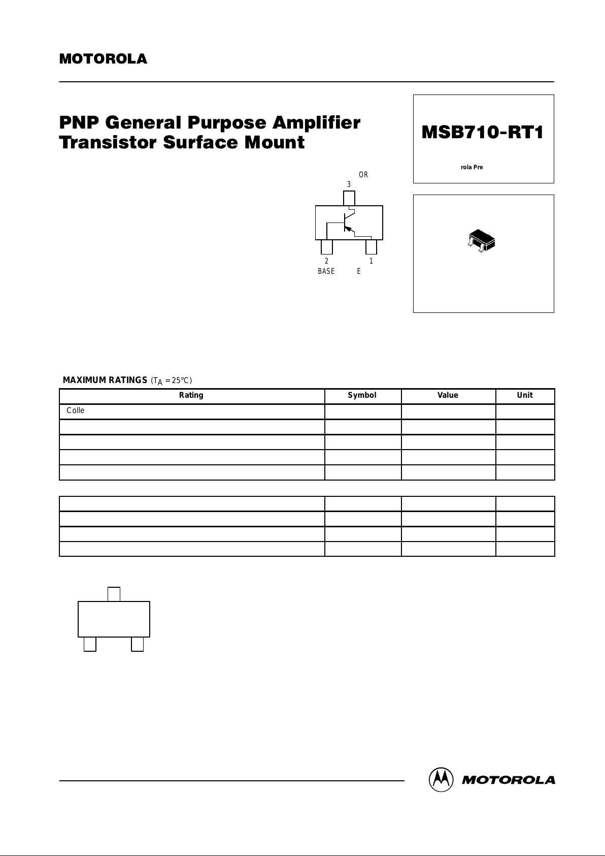
CASE 318D–04, STYLE 1
SC–59
2
1
3
COLLECTOR
3
2
BASE1EMITTER
replaces MSB710–QT1/D

MSB710-RT1
2
Motorola Small–Signal Transistors, FETs and Diodes Device Data
ELECTRICAL CHARACTERISTICS
(T
A
= 25°C)
Characteristic
Symbol Min Max Unit
Collector–Emitter Breakdown Voltage
(IC = –10 mAdc, IB = 0)
V
(BR)CEO
–50 — Vdc
Collector–Base Breakdown Voltage
(IC = –10 µAdc, IE = 0)
V
(BR)CBO
–60 — Vdc
Emitter–Base Breakdown Voltage
(IE = –10 µAdc, IC = 0)
V
(BR)EBO
–7.0 — Vdc
Collector–Base Cutoff Current
(VCB = –20 Vdc, IE = 0)
I
CBO
— –0.1 µAdc
DC Current Gain
(1)
(VCE = –10 Vdc, IC = –150 mAdc)
(VCE = –10 Vdc, IC = 500 mAdc)
h
FE1
h
FE2
120
40
240
—
—
Collector–Emitter Saturation Voltage
(IC = –300 mAdc, IB = –30 mAdc)
V
CE(sat)
— –0.6 Vdc
Collector–Base Saturation Voltage
(IC = –300 mAdc, IB = –30 mAdc)
V
BE(sat)
— –1.5 Vdc
Output Capacitance
(VCB = –10 Vdc, IE = 0, f = 1.0 MHz)
C
ob
— 15 pF
1. Pulse Test: Pulse Width ≤ 300 µs, D.C. ≤ 2%.
 Loading...