Motorola MRFIC2404 Datasheet

SEMICONDUCTOR TECHNICAL DATA
The MRFIC Line
The MRFIC2404 is a single–stage class A GaAs amplifier in a low–cost
8 lead plastic package designed to drive the MRFIC2403 power amplifier for
use in the 2.4 to 2.5 GHz Industrial–Scientific–Medical (ISM) band. The design
is optimized for 5.0 Volt operation at 2.45 GHz but is usable from 2.0 to 3.0 GHz
in applications such as telemetry and Multichannel Multipoint Distribution
System (MMDS) wireless cable TV systems. Performance is suitable for
frequency hopping or direct sequence spread spectrum as well as single–frequency applications.
• High Output Capability = +5.0 dBm Typical
• High Gain = 17 dB Typical
• Low Current Drain = 9.0 mA Typical
• Single Supply Voltage = 5.0 Volts
• Good Noise Figure = 4.3 dB Typical
• Low–Cost, Low Profile Plastic SOIC Package
• Order MRFIC2404R2 for Tape and Reel.
R2 Suffix = 2,500 Units per 12 mm, 13 inch Reel.
• Device Marking = M2404
Order this document
by MRFIC2404/D
2.4 GHz
EXCITER AMPLIFIER
GaAs MONOLITHIC
INTEGRATED CIRCUIT
CASE 751-05
(SO-8)
ABSOLUTE MAXIMUM RATINGS
Supply Voltage V
RF Input Power RF IN +10 dBm
Bias Enable Voltage V
Ambient Operating Temperature T
Storage Temperature T
(TA = 25_C unless otherwise noted)
Parameter Symbol Value Unit
12 Vdc
6.0 Vdc
–30 to +85
–65 to +125
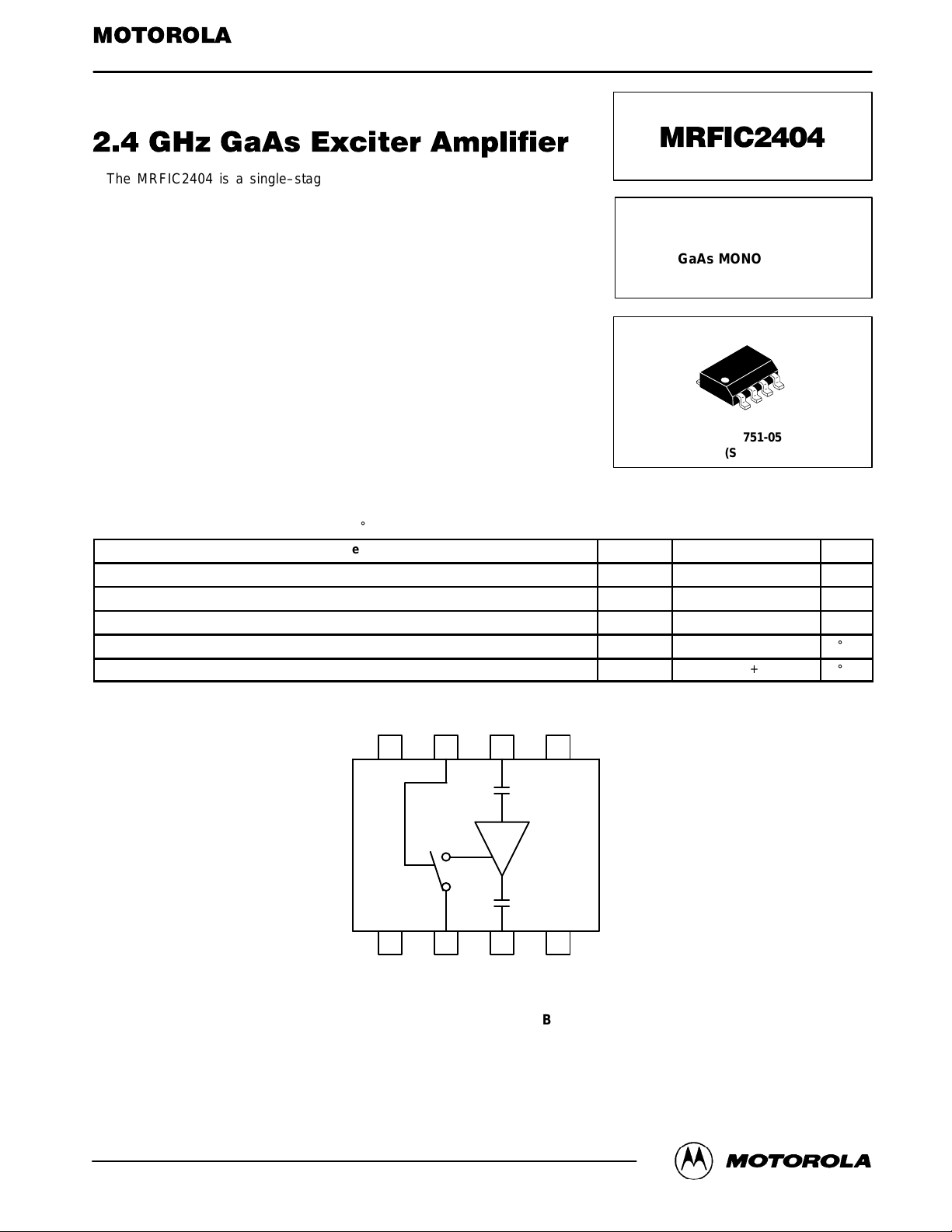
GND GND
8
1
GND GND
BIAS
DD
RF INV
7 6 5
2 3 4
RF OUTV
DD
bias
A
stg
_
C
_
C
REV 2
Motorola, Inc. 1995
Pin Connections and Functional Block Diagram
MRFIC2404MOTOROLA RF DEVICE DATA
1

RECOMMENDED OPERATING CONDITIONS
Parameter Symbol Value Unit
Supply Voltage V
Bias Enable Voltage – ON V
Bias Enable Voltage – OFF V
Operating Frequency Range f
DD
bias
bias
OP
4.75 to 5.25 Vdc
0 Vdc
5.0 Vdc
2000 to 3000 MHz
ELECTRICAL CHARACTERISTICS (V
Characteristic Min Typ Max Unit
Small Signal Gain 16 17 – dB
Power Output, 1.0 dB Compression – +5.0 – dBm
Power Output (Pin = –11 dBm) 4.0 5.0 – dBm
Third Order Intercept Point – +15 – dBm
Noise Figure – 4.3 – dB
Reverse Isolation – 25 – dB
Turn On Time – 1.0 –
Supply Current – 9.0 12 mA
SLEEP Mode Supply Current (V
= 5.0 Vdc) – 800 –
bias
RF IN
V
BIAS
= 5.0 Vdc, TA= 25_C, RF = 2.45 GHz, V
DD
5
6
7
8
4
3
2
1
bias
T1
= 0 Vdc)
C1
V
DD
RF OUT
m
s
m
A
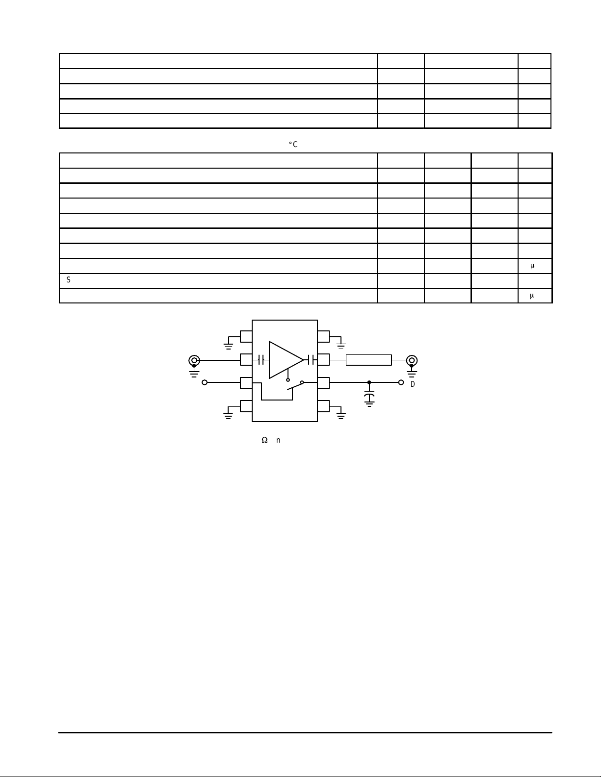
C1 – 15 pF
T1 – 100 W Line, 185 MILs (3.3 nH)
Board Material – 30 MIL FR4
Connectors – SMA Type
Figure 1. Applications Circuit Configuration
MRFIC2404
2
MOTOROLA RF DEVICE DATA
 Loading...