Motorola MRFIC2403 Datasheet

SEMICONDUCTOR TECHNICAL DATA
The MRFIC Line
The MRFIC2403 is a two–stage class B GaAs power amplifier in a low–cost
16 lead plastic package designed for use in the 2.4 to 2.5 GHz Industrial–
Scientific–Medical (ISM) band. The design is optimized for efficiency at 5.0 V olt
operation at 2.5 GHz but is usable from 2.0 to 3.0 GHz in applications such as
telemetry and Multichannel Multipoint Distribution System (MMDS) wireless
cable TV systems. Performance is suitable for frequency hopping or direct
sequence spread spectrum as well as single–frequency applications. Power
control circuitry allows 20 dB dynamic range for setting the output power.
• High Output Power = +23.5 dBm Typical
• High Gain = 23 dB Typical
• Excellent Efficiency = 55% Typical
• Power Control = 20 dB Range
• Low–Cost, Low Profile Plastic SOIC Package
• Available in Tape and Reel by Adding R2 Suffix to Part Number.
R2 Suffix = 2,500 Units per 16 mm, 13 inch Reel.
• Device Marking = M2403
Order this document
by MRFIC2403/D
2.4 GHz
POWER AMPLIFIER
GaAs MONOLITHIC
INTEGRATED CIRCUIT
CASE 751B-05
(SO–16)
ABSOLUTE MAXIMUM RATINGS
Supply Voltage V
Power Control Voltage V
Gate Bias Voltage VG1, V
RF Input Power RF IN +10 dBm
Ambient Operating Temperature T
Storage Temperature T
(TA = 25_C unless otherwise noted)
Parameter Symbol Value Unit
6.0 Vdc
6.0 Vdc
–4.0 Vdc
–30 to +85
–65 to +125
RF OUT
N/C GND GND GND V
16
15 14 13 12 11 10 9
V
D2
G2
DD
CONTRL
G2
A
stg
GND V
G1
_
C
_
C
REV 1
Motorola, Inc. 1995
1
V
DD
2 3 4 5 6 7 8
GND PCNTRL GND GND RF IN GND N/C
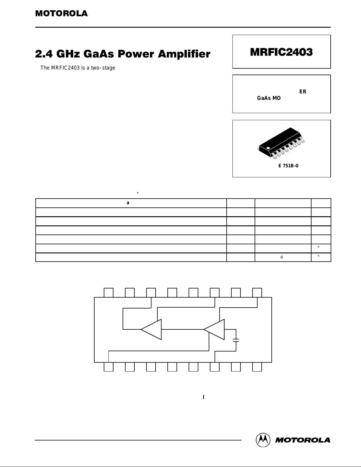
Pin Connections and Functional Block Diagram
MRFIC2403MOTOROLA RF DEVICE DATA
1

RECOMMENDED OPERATING CONDITIONS
Parameter Symbol Value Unit
Supply Voltage V
Gate Bias Voltage, Input Stage V
Gate Bias Voltage, Output Stage V
Quiescent Drain Current, Stage One I
Quiescent Drain Current, Stage Two I
Operating Frequency Range f
DD
G1
G2
DQ1
DQ2
OP
4.75 to 5.25 Vdc
–1.0 Vdc
–2.0 Vdc
12 mA
10 mA
2200 to 2700 MHz
ELECTRICAL CHARACTERISTICS (V
5.0 Vdc)
Characteristic
Small Signal Gain (Pin = –6.0 dBm) – 23 – dB
Power Output (Pin = +4.0 dBm) 23 23.5 – dBm
Power Output, Saturation – 23.5 – dBm
Power Output, 1.0 dB Compression – 19 – dBm
2nd Harmonic Output – –20 – dBc
3rd Harmonic Output – –30 – dBc
Third Order Intermodulation Products (Pin = +4.0 dBm PEP) – –15 – dBc
Reverse Isolation – 32 – dB
Power Control Range, PCNTRL – 20 – dB
Reverse Isolation – 30 – dB
Supply Current – 95 140 mA
SLEEP Mode Supply Current (VG1 = VG2 = –3.0 Vdc, PCNTRL = 0 Vdc) – 150 –
V
G1
= 5.0 V d c , TA = 25_C, RF = 2.45 GHz @ +4.0 dBm, VG1 = –1.0 Vdc, VG2 = –2.0 Vdc, PCNTRL =
DD
Min Typ Max Unit
9
10
8
7
m
A
RF OUT
MRFIC2403
2
V
V
G2
DD2
C3
C6
C5
L1
C4
11
12
13
14
15
16
6
5
4
3
2
1
C2
C1
RF IN
PCNTRL
V
D1
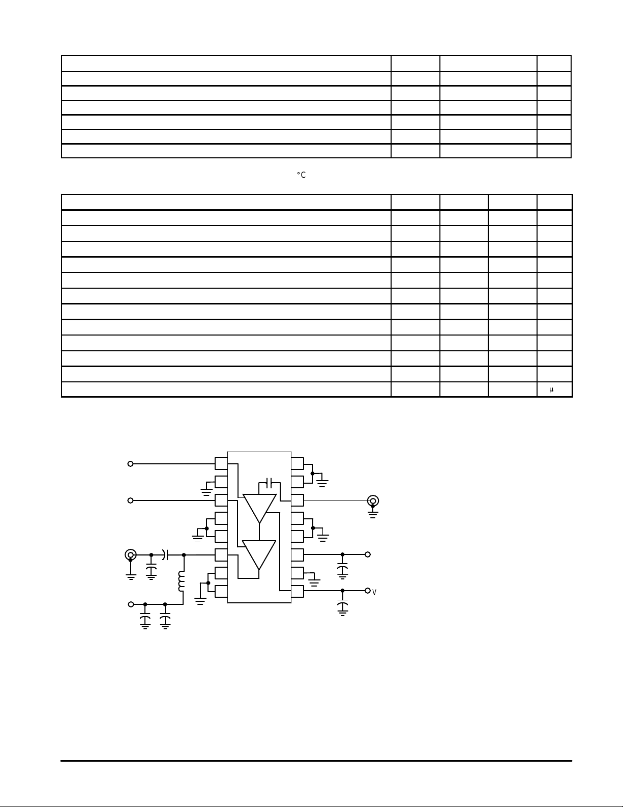
Figure 1. Applications Circuit Configuration
C1, C2, C3 – 0.01 µF
C4 – 5.1 pF
C5 – 15 pF
C6 – 1.0 pF
L1 – 6.8 nH
Board Material – 30 MIL FR4
Connectors – SMA type
MOTOROLA RF DEVICE DATA
 Loading...