SEMICONDUCTOR TECHNICAL DATA
The MRFIC Line
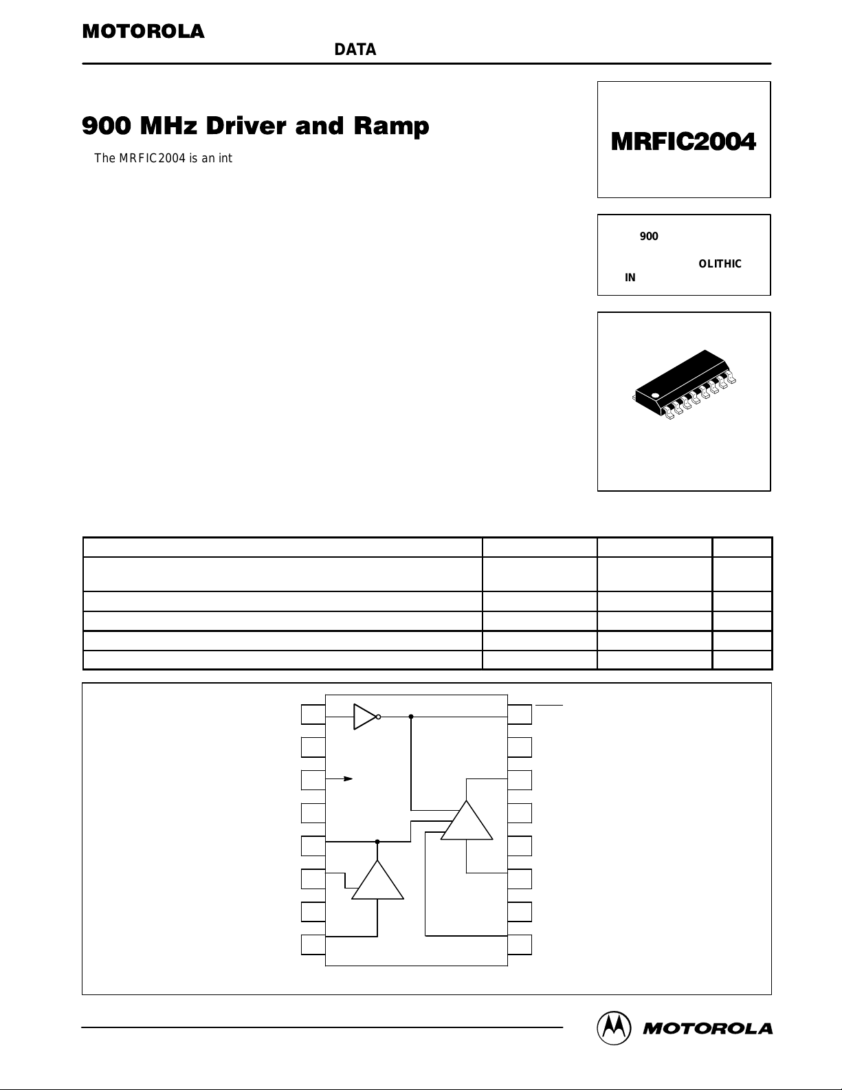
The MRFIC2004 is an integrated Driver and Ramp designed for transmitters
operating in the 800 MHz to 1.0 GHz frequency range. The Ramp is an
integrator which can be used for burst control for TDD/TDMA systems. The
Driver uses a cascode configuration for high gain and reverse isolation. A power
down control is provided to minimize current drain with minimum recovery/turnon time. Also, an on-board inverter is included to provide complementary
control for an antenna switch, such as the MRFIC2003. The design utilizes
Motorola’s advanced MOSAIC 3 silicon bipolar RF process to yield superior
performance in a cost effective monolithic device. Applications for the
MRFIC2004 include CT1 and CT2 cordless telephones, GSM, remote controls,
video and audio short range links, low cost cellular radios, and ISM band
transmitters.
• Small Signal Gain = 21.5 dB (Typ)
• Small Signal Gain Control = 34 dB (Typ)
• Po
• On Board Ramp for Burst Control
• Power Down Supply Current = 0.7 mA (Typ)
• Low Operating Supply Voltage (2.7 to 4.0 Volts)
• Input/Output VSWR Insensitive to Gain Control
• Order MRFIC2004R2 for Tape and Reel.
R2 Suffix = 2,500 Units per 16 mm, 13 inch Reel.
• Device Marking = M2004
= –1.0 dBm (Typ)
1.0 dB
Order this document
by MRFIC2004/D
900 MHz DRIVER
& RAMP
SILICON MONOLITHIC
INTEGRATED CIRCUIT
CASE 751B-05
(SO-16)
ABSOLUTE MAXIMUM RATINGS
Supply Voltages V
Control Voltages RXEN, TXEN, V
Input Power, RF IN Port P
Operating Ambient Temperature T
Storage Temperature T
(TA = 25°C unless otherwise noted)
Rating Symbol Value Unit
CC1
V
CC2
RF
A
stg
GND
V
CC1
GND
V
RAMP
C INT
GND
1RX EN
2
3
4
DRIVER
5
6
RAMP
7
RX EN
16
GND
15
RF OUT/V
14
GND
13
GND
12
RF IN
11
GND
10
cont
CC2
4.5
6.0
6.0 Vdc
+10 dBm
–35 to +85 °C
–65 to +150 °C
Vdc
REV 2
Motorola, Inc. 1997
TX EN
8
9
Pin Connections and Functional Block Diagram
V
cont
(GAIN CONTROL)
MRFIC2004MOTOROLA RF DEVICE DATA
1

RECOMMENDED OPERATING RANGES
Parameter Symbol Value Unit
Supply Voltage Ranges V
Control Voltage Ranges TX EN, RX EN,
Frequency Range f 800 to 1000 MHz
ELECTRICAL CHARACTERISTICS (V
Characteristics (1)
Supply Current, TX EN High, RX EN Low — 11 13 mA
Supply Current, TX EN Low, RX EN High — 0.7 1.5 mA
Driver Characteristics (1)
Gain (Small Signal) 19 21.5 24 dB
Gain Control (Small Signal) — 34 — dB
Power Out @ 1.0 dB Gain Compression –4.0 –1.0 — dBm
Third Order Intercept Point (out) — +7.5 — dBm
Reverse Isolation — 32 — dB
Ramp Characteristics (1)
Ramp Up Delay Time
Rise Time
Total Time
Ramp Down Delay Time
Fall Time
Total Time
LOGIC LEVELS (V
High
Low
High
Low
NOTE:
1. All electrical characteristics measured in test circuit schematic shown in Figure 1 below.
= 2.7 to 4.0 V, TA = 25°C)
CC1
RX EN & TX EN Input Voltage
RX EN Output Voltage
CC1
, V
CC2
= 3.0 V, C
= 2.0 nF, TA = 25°C, f = 900 MHz, V
INT
V
V
, V
CC1
CC2
V
cont
Min Typ Max Unit
—
—
—
—
—
—
Min Typ Max Unit
– 0.8
CC1
—
– 0.2
CC1
—
4.0
18
22
4.0
18
22
—
—
—
—
2.7 to 4.0 Vdc
0 to V
CC1
= 1.3 V)
CONT
—
—
—
—
—
—
—
0.8
—
0.2
Vdc
µs
µs
V
V
MRFIC2004
2
MOTOROLA RF DEVICE DATA

TX EN
f
V
cont
+
V
RAMP
–
C
C6
INT
+
–
D.U.T.
+
–
C9
C5 C7
12345678
161514131211109
L2
+
VCC 1
–
+
RX EN
–
+
RX EN
–
Ω
LINE
RF IN
50
Ω
C1, C7, C9 — 1000 pF Chip Capacitor
C2, C5, C6, C10 — 100 pF Chip Capacitor
C3 — 1.6 pF Chip Capacitor
C
— 2000 pF Chip Capacitor
INT
50
C10C11
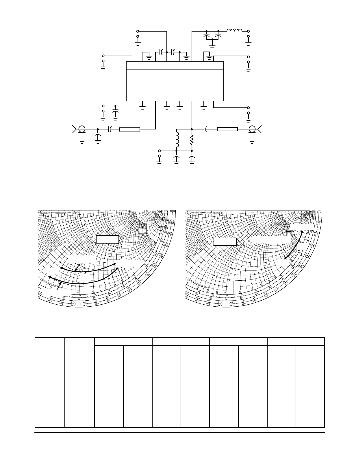
Figure 1. T ypical Biasing Configuration
Zo = 50
Ω
V
= 1.0 V
cont
1000
750
f = 500 MHz
L1 R1
+
VCC 2
–
C11 — 6.2 pF Chip Capacitor
L1 — 4.7 nH Chip Inductor
L2 — 150 nH Chip Inductor
R1 — 330 Ω Chip Resistor
C3
C2C1
Ω
LINE
50
RF Connectors — SMA Type
Board Material — Epoxy/Glass εr= 4.5,
Dielectric Thickness = 0.014″ (0.36 mm)
Zo = 50
Ω
RF OUT
50
V
= 1.0 or 3.0 V
cont
Ω
f = 500 MHz
1000
750
V
= 3.0 V
cont
Figure 2. S11 versus Frequency versus V
S
f
V
cont
1.0 100 0.85 –11.3 10.48 –171.5 0.0002 142.7 0.99 –2.9
(MHz)
300 0.83 –32.8 10.33 –156.3 0.0020 129.0 0.99 –7.3
500 0.79 –56.9 10.15 –140.5 0.0030 130.6 0.98 –15.9
550 0.79 –62.5 10.04 –135.9 0.0030 132.6 0.98 –17.9
600 0.78 –68.5 9.85 –130.2 0.0040 133.3 0.98 –20.0
650 0.77 –74 9.47 –126.9 0.0040 135.9 0.98 –22.3
700 0.76 –79 9.23 –123.6 0.0050 137.2 0.98 –24.7
750 0.76 –84.4 9.02 –119.4 0.0050 138.1 0.97 –27.0
800 0.75 –89.6 8.69 –113.8 0.0060 139.7 0.97 –29.3
850 0.74 –94.5 8.33 –110.8 0.0070 140.3 0.97 –31.4
900 0.73 –99.1 8.13 –108.9 0.0080 141.2 0.96 –33.2
950 0.73 –102 7.98 –105.4 0.0090 138.3 0.96 –36.3
|S11| ∠φ |S21| ∠φ |S12| ∠φ |S22| ∠φ
11
cont
S
21
Figure 3. S22 versus Frequency
S
12
S
22
MRFIC2004MOTOROLA RF DEVICE DATA
3
 Loading...