Motorola MRFIC2002 Datasheet

SEMICONDUCTOR TECHNICAL DATA
The MRFIC Line
The MRFIC2002 is a double-balanced, active mixer designed for transmitters
operating in the 800 MHz to 1.0 GHz frequency range. The design utilizes
Motorola’s advanced MOSAIC 3 silicon bipolar RF process to yield superior
performance in a cost effective monolithic device. Applications for the
MRFIC2002 include CT1 and CT2 cordless telephones, GSM, remote controls,
video and audio short range links, low cost cellular radios, and ISM band
transmitters. A power down control is provided to minimize current drain with
minimum recovery/turn-on time.
• Conversion Gain = 10 dB (Typ)
• Supply Current = 5.5 mA (Typ)
• Power Down Supply Current = 2.0 µA (Max)
• LO-RF Isolation = 25 dB (Typ)
• Low LO Drive Required = –10 dBm (Typ)
• LO Impedance Insensitive to Power Down
• No Matching Required for RF OUT Port
• All Ports are Single Ended
• Order MRFIC2002R2 for Tape and Reel.
R2 Suffix = 2,500 Units per 12 mm, 13 inch Reel.
• Device Marking = M2002
Order this document
by MRFIC2002/D
900 MHz TX-MIXER
SILICON MONOLITHIC
INTEGRATED CIRCUIT
CASE 751-05
(SO-8)
ABSOLUTE MAXIMUM RATINGS
Supply Voltage V
Control Voltages ENABLE, V
Input Power, LO and IF Ports PLO, P
Operating Ambient Temperature T
Storage Temperature T
(TA = 25°C unless otherwise noted)
Rating Symbol Value Unit
IF IN
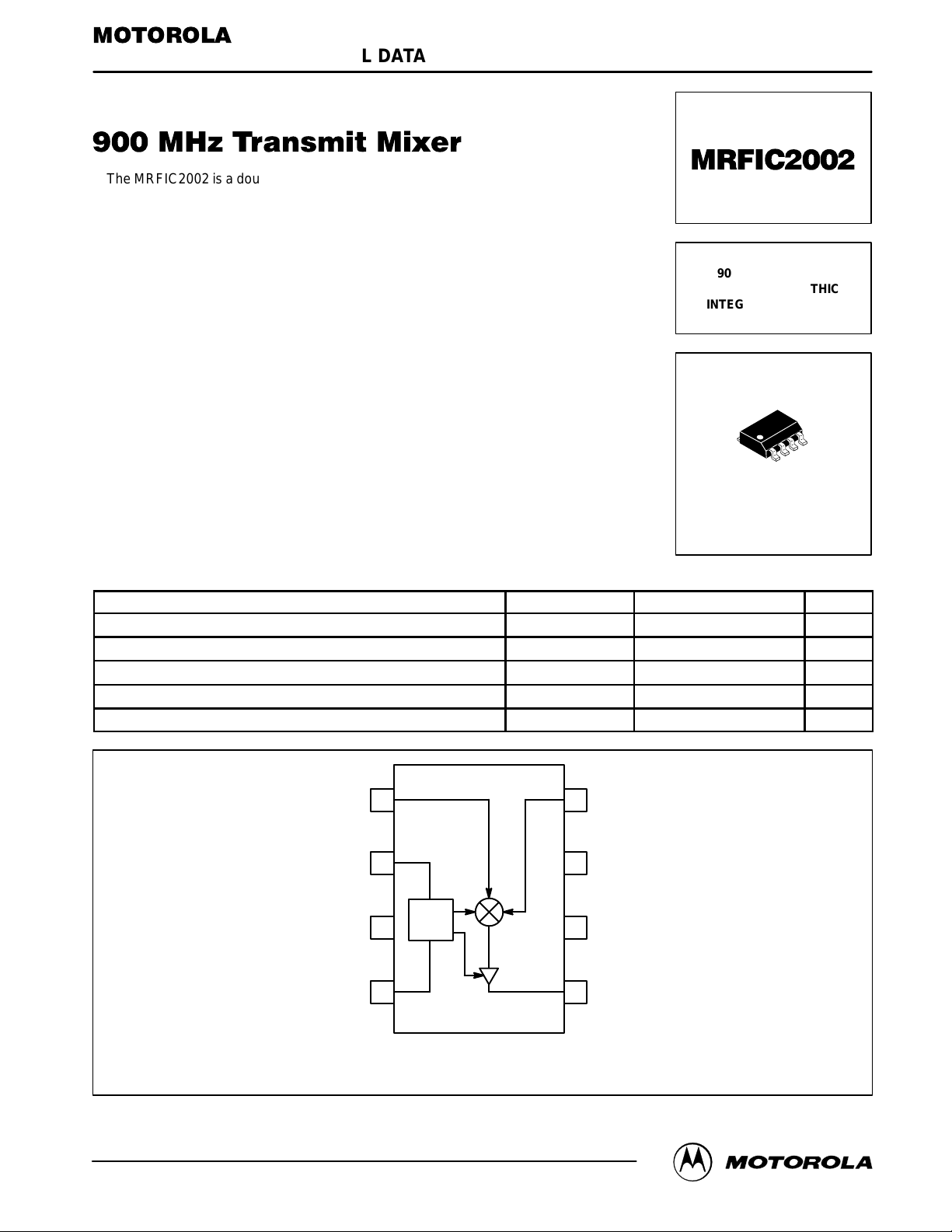
1 8
(1)
V
RAMP
ENABLE
2 7
GND
BIAS
3 6
CNTL
4 5
CC
A
stg
RAMP
IF
LO IN
V
CC
GND
RF OUT
5.5 Vdc
5.0 Vdc
+10 dBm
–35 to +85 °C
–65 to +150 °C
REV 2
Motorola, Inc. 1997
(1) For CT2 applications, apply ramp voltage provided in MRFIC2004. For non-CT2, leave open circuited.
Pin Connections and Functional Block Diagram
MRFIC2002MOTOROLA RF DEVICE DATA
1

RECOMMENDED OPERATING RANGES
Parameter Symbol Value Unit
Supply Voltage Range V
Control Voltage Ranges ENABLE, V
RF Port Frequency Range f
IF Port Frequency Range f
ELECTRICAL CHARACTERISTICS (V
GHz, RF @ 900 MHz, TA = 25°C unless otherwise noted)
Characteristic (2)
Supply Current: On-Mode
Supply Current: Off-Mode (Enable < 1.0 V)
Enable Response Time — 1.0 — µs
Conversion Gain 8.0 10 12 dB
Single Sideband Noise Figure — 10 — dB
Output Power at 1.0 dB Gain Compression — –18 — dBm
Output Power at Saturation –16 –14 — dBm
LO-RF Isolation (1.0 GHz) — 25 — dB
LO-IF Isolation (1.0 GHz) — 65 — dB
IF-RF Isolation (100 MHz) — 18 — dB
IF-LO Isolation (100 MHz) — 50 — dB
NOTES:
1. For CT2 applications, apply ramp voltage provided in MRFIC2004. For non-CT2, leave open circuited.
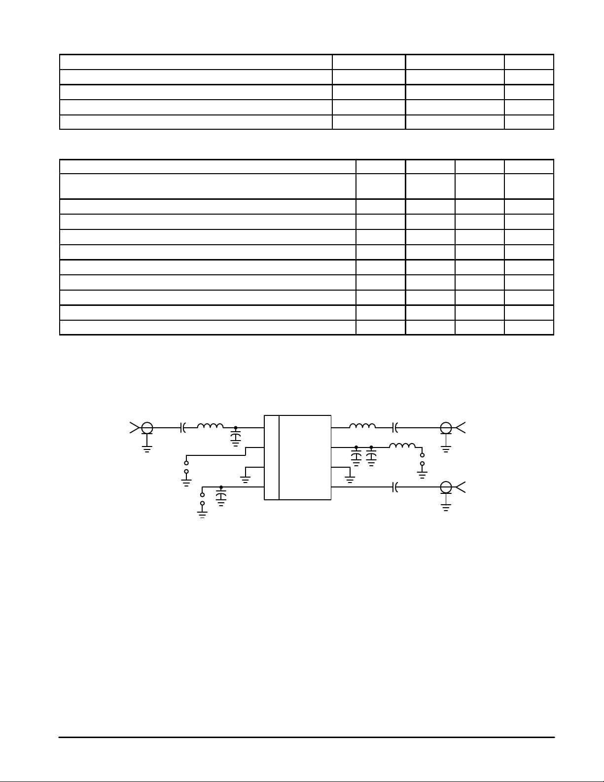
2. All Electrical Characteristics are measured in test circuit schematic as shown in Figure 1.
, Enable = 3.0 V and V
CC
Ramp
(1)
Open Circuited, PLO = –7.0 dBm, IF @ 100 MHz, LO @ 1.0
CC
RAMP
RF
IF
Min Typ Max Unit
—
—
2.7 to 5.0 Vdc
0 to 5.0 Vdc
500 to 1000 MHz
0 (dc) to 250 MHz
5.5
0.1
7.0
2.0
mA
µA
IF IN
Ω
50
C1 L1 L2
C2
V
+
*
RAMP
–
ENABLE
C1, C3, C6 — 1000 pF Chip Capacitor
C2 — 6.8 pF Chip Capacitor
C4 — 3.9 pF Chip Capacitor
C5 — 100 pF Chip Capacitor
C7 — 5.6 pF Chip Capacitor
L1 — 270 nH Chip Inductor
+
–
C3
1
2
3
4
8
7
D.U.T.
6
5
L2 — 10 nH Chip Inductor
L3 — 390 nH Chip Inductor
RF Connectors — SMA Type
Board Material — Glass/Epoxy εr = 4.5,
Dielectric Thickness = 0.014″ (0.36 mm)
Figure 1. T est Circuit
Configuration
C4
L3
C6C5
C7
+
–V
CC
LO IN
50
Ω
RF OUT
50
Ω
MRFIC2002
2
MOTOROLA RF DEVICE DATA
 Loading...