

Motorola MRFIC1818 Datasheet
SEMICONDUCTOR TECHNICAL DATA
The MRFIC Line
Order this document
by MRFIC1818/D
Designed specifically for application in Pan European digital 1.0 watt DCS1800
handheld radios, the MRFIC1818 is specified for 33 dBm output power with power
gain over 30 dB from a 4.8 volt supply . With minor tuning changes, the MRFIC1818
can be used for PCS1900 as well as PCS CDMA. To achieve this superior
performance, Motorola’s planar GaAs MESFET process is employed. The device
is packaged in the PFP–16 Power Flat Package which gives excellent thermal
and electrical performance through a solderable backside contact while allowing
the convenience and cost benefits of reflow soldering.
• Minimum Output Power Capabilities
33 dBm @ 4.8 Volts
32 dBm @ 4.0 Volts
• Specified 4.8 Volt Characteristics
RF Input Power = 3.0 dBm
RF Output Power = 33 dBm
Minimum PAE = 35%
• Low Current required from Negative Supply – 2 mA max
• Guaranteed Stability and Ruggedness
• Order MRFIC1818R2 for Tape and Reel.
R2 Suffix = 1,500 Units per 16 mm, 13 inch Reel.
• Device Marking = M1818
ABSOLUTE MAXIMUM RATINGS
DC Positive Supply Voltage V
DC Negative Supply Voltage V
RF Input Power P
RF Output Power P
Operating Case Temperature Range T
Storage Temperature Range T
Thermal Resistance, Junction to Case R
(TA = 25°C, ZO = 50 Ω, unless otherwise noted)
Rating
Symbol Value Unit
D1, 2, 3
stg
θJC
SS
in
out
C
1700–1900 MHz MMIC
DCS1800/PCS1900
INTEGRATED POWER AMPLIFIER
GaAs MONOLITHIC
INTEGRATED CIRCUIT
CASE 978–02
(PFP–16)
7.5 Vdc
–5 Vdc
10 dBm
36 dBm
–35 to +85 °C
–55 to +150 °C
10 °C/W
REV 2
Motorola, Inc. 1997
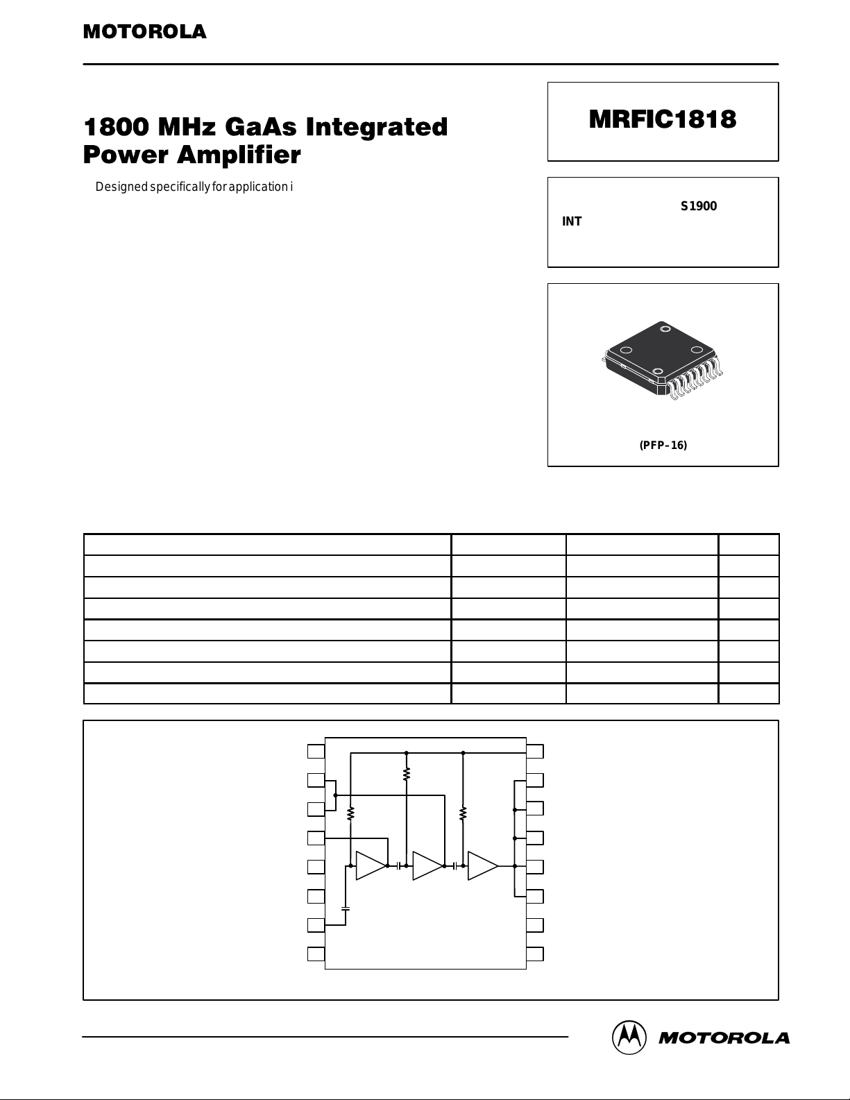
GND
V
D2
V
D2
V
D1
N/C
GND
RF IN
N/C
9
10
11
12
13
14
15
16
8
7
6
5
4
3
2
1
Pin Connections and Functional Block Diagram
V
G
V
D3
RF OUT
RF OUT
RF OUT
RF OUT
N/C
GND
MRFIC1818MOTOROLA RF DEVICE DATA
1
RECOMMENDED OPERATING RANGES
Parameter Symbol Value Unit
Supply Voltage V
Gate Voltage V
RF Frequency Range f
RF Input Power P
D1, 2, 3
SS
RF
RF
2.7 to 6 Vdc
–3.5 to –4.5 Vdc
1700 to 1900 MHz
0 to 6 dBm
ELECTRICAL CHARACTERISTICS (V
= 4.8 V, VSS = –4 V, Pin = 3 dBm, Peak Measurement at 12.5% Duty Cycle, 4.6 ms
D1, 2, 3
Period, TA = 25°C unless otherwise noted. Measured in Reference Circuit Shown in Figure 1.)
Characteristic
Min Typ Max Unit
Frequency Range 1710 — 1785 MHz
Output Power 33 34.5 — dBm
Power Added Efficiency 35 42 — %
Output Power (Tuned for PCS Band, 1850 to 1910 MHz) — 34.5 — dBm
Power Added Efficiency (Tuned for PCS Band, 1850 to 1910 MHz) — 42 — %
Input VSWR — 2:1 — VSWR
Harmonic Output (2nd and 3rd) — –35 –30 dBc
Output Power at Low voltage (VD1, VD2, VD3= 4.0 V) 32 33 — dBm
Output Power, Isolation (VD1, VD2, VD3 = 0 V) — –40 –35 dBm
Noise Power (In 100 kHz, 1805 to 1880 MHz) — –85 –80 dBm
Stability – Spurious Output (Pin = 5 dBm, P
VSWR = 6:1 at any Phase Angle, Source VSWR = 3:1, at any Phase Angle)
Load Mismatch stress (P
any Phase Angle)
= 33 dBm, Load VSWR = 10:1 at
out
(1)
= 0 to 33 dBm, Load
out
(1)
— — –60 dBc
No Degradation in Output Power after Returning to
Standard Conditions
3 dB VDD Bandwidth — 2 — MHz
Negative Supply Current — 0.7 2 mA
(1) Adjust V
(0 to 4.8 V) for specified P
D1, 2, 3
; Duty Cycle = 12.5%, Period = 4.6 ms.
out
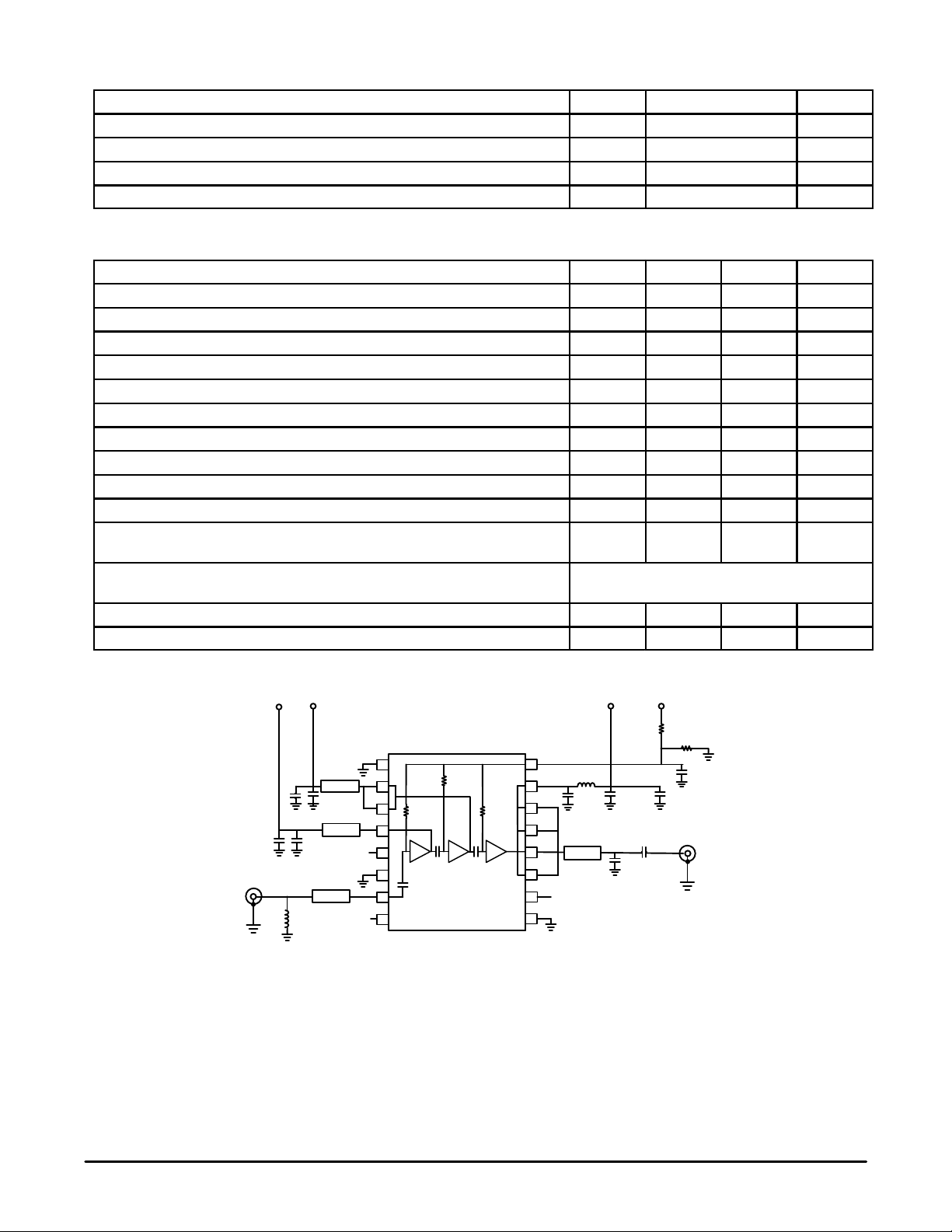
V
V
D2
D1
C9 C8
C7 C6
RF IN
L2
C1 6.8 nF
C2, C6, C8 22 pF, NPO/COG
C3, C7, C9 47 nF
C4 27 pF , NPO/COG
T2
NC
NC
9
10
11
12
13
14
15
16
T4
T3
C5 3.9 pF, NPO/COG
L1 18 nH, Coilcraft
L2 1.8 nH, Toko 2012
R1, R2 = 2.7 KΩ
8
7
6
5
4
3
2
1
C10
C10 0.5 pF
NOTE: For PCS/DCS1900 applications, the following components are used.
C5 = 2.7 pF, 0603 NPO/COG
L2 = 1.5 nH, Toko 2012
T3 = 1 mm 50 Ω Microstrip Line
Figure 1. Reference Circuit Configuration
V
L1
D3
R1
V
SS
R2
C1
C3C2
T1
C4
RF OUT
NC
C5
T1 1.4 mm 25 Ω Microstrip Line
T2 5 mm 50 Ω Microstrip Line
T3 4 mm 50 Ω Microstrip Line
T4 0.5 mm 50 Ω Microstrip Line
Board Material: Glass/Epoxy,
Thickness = 0.5 mm
ε
= 4.45,
r
MRFIC1818
2
MOTOROLA RF DEVICE DATA

0 V
0 V
C13
CR1
C15
C14
3.0 V
3.0 V
1
2
3
4
5
6
7
VRAMP
U2
V
reg
IDLE
R4
RF IN
D
5
6
7
8
R3
V
BAT
C18
14
13
C16
12
C17
11
10
9
8
C12
C19
C10
C9
L2
T2
T4
T3
R5
NC
NC
C11
9
10
11
12
13
14
15
16
IN
G
4
D
S
3
D
S
2
D
1
Q1
–4.0 V
R2R1
VG TUNE
8
L1
7
6
5
4
3
2
1
T1
NC
C1
C3C2
C4
RF
OUT
C6
C1 6.8 nF
C2, C9, C10 22 pF, 0603 NPO/COG
C3, C11 47 nF
C4 27 pF, 0603 NPO/COG
C14, C15 1 µF
C18 1 µF
CR1 MMBD701L T1
L1 18 nH, Coilcraft or 20 mm
C6 3.9 pF, 0603 NPO/COG
C12 220 nF
L2 1.8 nH, Toko 2012
C13, C16, C17, C19 1 µF
Q1 MMSF4N01HD
R1, R2 2.7 kΩ
NOTE: For PCS/DCS1900 applications, the following
component values are changed.
C6 = 2.7 pF, 0603 NPO/COG
L2 = 1.5 nH, Toko 2012
T3 = 1 mm 50 Ω Microstrip Line
Figure 2. DCS1800 Applications Circuit Configuration
50 Ω Microstrip Line
or 5 mm 50 Ω Line
U1
R3, R4 100 Ω
R5 470 Ω
T1 2 mm 25 Ω Microstrip Line
T2 5 mm 50 Ω Microstrip Line
T3 8 mm 40 Ω Microstrip Line
T4 1 mm 40 Ω Microstrip Line
U1 MRFIC1818
U2 MC33169 (–4 V Version)
Board Material: Glass/Epoxy,
Thickness = 0.5 mm
ε
= 4.45,
r
MRFIC1818MOTOROLA RF DEVICE DATA
3
 Loading...