Motorola MRFIC1817 Datasheet

SEMICONDUCTOR TECHNICAL DATA
The MRFIC Line
!
Order this document
by MRFIC1817/D
Designed specifically for application in Pan European digital 1.0 watt
DCS1800/PCS1900 handheld radios, the MRFIC1817 is specified for 32 dBm
output power with power gain over 27 dB from a 3.6 volt supply . To achieve this
superior performance, Motorola’s planar GaAs MESFET process is employed.
The device is packaged in the PFP–16 Power Flat Package which gives
excellent thermal and electrical performance through a solderable backside
contact while allowing the convenience and cost benefits of reflow soldering.
• Minimum Output Power Capabilities
32 dBm @ 3.6 Volts
30 dBm @ 3.0 Volts
• Typical Volt Characteristics
RF Input Power = 5.0 dBm
RF Output Power = 33.5 dBm
Typical PAE = 42%
• Low Current required from Negative Supply – 2 mA max
• Guaranteed Stability and Ruggedness
• Order MRFIC1817R2 for Tape and Reel.
R2 Suffix = 1,500 Units per 16 mm, 13 inch Reel.
• Device Marking = M1817
ABSOLUTE MAXIMUM RATINGS
DC Positive Supply Voltage V
DC Negative Supply Voltage V
RF Input Power P
RF Output Power P
Operating Case Temperature Range T
Storage Temperature Range T
Thermal Resistance, Junction to Case R
(TA = 25°C, ZO = 50 Ω, unless otherwise noted)
Rating
Symbol Value Unit
D1, 2, 3
stg
θJC
SS
in
out
C
1700–1900 MHz MMIC
DCS1800/PCS1900
INTEGRATED POWER AMPLIFIER
GaAs MONOLITHIC
INTEGRATED CIRCUIT
CASE 978–02
(PFP–16)
6 Vdc
–5 Vdc
10 dBm
35 dBm
–35 to +85 °C
–55 to +150 °C
10 °C/W
Motorola, Inc. 1997
GND
V
D2
V
D2
V
D1
N/C
GND
RF IN
N/C
9
10
11
12
13
14
15
16
8
7
6
5
4
3
2
1
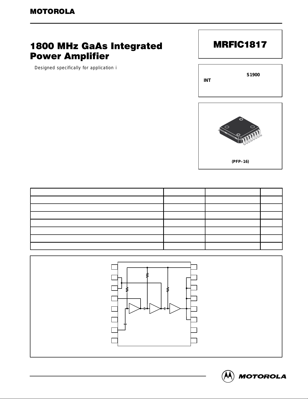
Pin Connections and Functional Block Diagram
V
G
V
D3
RF OUT
RF OUT
RF OUT
RF OUT
N/C
GND
MRFIC1817MOTOROLA RF DEVICE DATA
1

RECOMMENDED OPERATING RANGES
Parameter Symbol Value Unit
Supply Voltage V
Gate Voltage V
RF Frequency Range f
RF Input Power P
D1, 2, 3
SS
RF
RF
2.7 to 5 Vdc
–3.5 to –4.5 Vdc
1700 to 1900 MHz
0 to 6 dBm
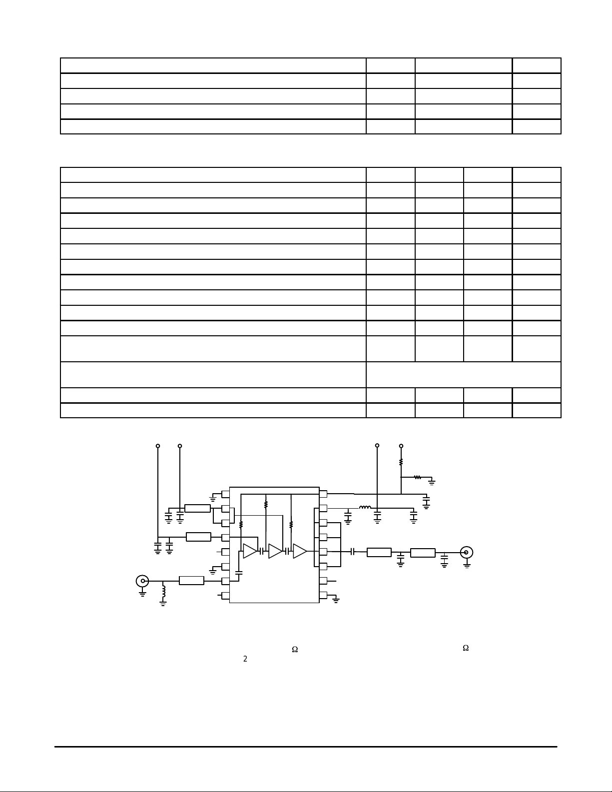
ELECTRICAL CHARACTERISTICS (V
= 3.6 V, VSS = –4 V, Pin = 5 dBm, Peak Measurement at 12.5% Duty Cycle, 4.6 ms
D1, 2, 3
Period, TA = 25°C unless otherwise noted. Measured in Reference Circuit Shown in Figure 1)
Characteristic
Min Typ Max Unit
Frequency Range 1710 — 1785 MHz
Output Power 32 33.5 — dBm
Power Added Efficiency 35 42 — %
Output Power (PCS 1900 Tuning f = 1850 to 1910 MHz) — 33.5 — dBm
Power Added Efficiency (PCS 1900 Tuning f = 1850 to 1910 MHz) — 42 — %
Input VSWR — 2:1 — VSWR
Harmonic Output (2nd and 3rd) — –35 –30 dBc
Output Power at Low voltage (VD1, VD2, VD3 = 3.0 V) 30 32 — dBm
Output Power Isolation (VD1, VD2, VD3 = 0 V) — –40 –30 dBm
Noise Power (In 100 kHz, 1805 to 1880 MHz) — –85 –80 dBm
Stability – Spurious Output (Pin = 5 dBm, P
VSWR = 6:1 at any Phase Angle, Source VSWR = 3:1, at any Phase Angle)
Load Mismatch stress (P
any Phase Angle)
= 33 dBm, Load VSWR = 10:1 at
out
(1)
= 0 to 33 dBm, Load
out
(1)
— — –60 dBc
No Degradation in Output Power after Returning to
Standard Conditions
3 dB VDD Bandwidth — 2 — MHz
Negative Supply Current — 0.7 2 mA
(1) Adjust V
(0 to 3.6 V) for specified P
D1, 2, 3
V
D1
; Duty Cycle = 12.5%, Period = 4.6 ms.
out
V
D2
V
V
D3
SS
9
T4
T3
NC
NC
10
11
12
13
14
15
16
L1 18 nH, Coilcraft or 20 mm
50 Ω Microstrip Line
L2 1.8 nH, Toko 2012
R1 2.7 K
W
R2 2.2 KΩ
T1 2.5 mm 50 Ω Microstrip Line
C9 C8
C7 C6
T2
RF IN
L2
C1 1 nF
C2, C6, C8 22 pF, NPO/COG
C3, C7, C9 47 nF
C4 5.6 pF, AVX0603 ACCUF
C5 3.9 pF, AVX0603 ACCUF
C10, C11 1 pf
NOTE: For PCS 1900 tuning the following values are changed.
C5 = 2.7 pF, AVX0603 ACCUF
L2 = 1.5 nH, Toko 2012
T3 = 1 mm 50 Ω Microstrip Line
Figure 1. Reference Circuit Configuration
R1
R2
8
7
6
5
4
3
2
1
NC
C4
L1
C11
T1
C5
C1
C3C2
T5
RF
OUT
C10
T2 6 mm 50 Ω Microstrip Line
T3 5 mm 40 Ω Microstrip Line
T4 1 mm 40 Ω Microstrip Line
T5 5.5 mm 50 W Microstrip Line
ε
Board Material: Glass/Epoxy,
Thickness = 0.5 mm
= 4.45,
r
MRFIC1817
2
MOTOROLA RF DEVICE DATA

0 V
0 V
C13
CR1
C15
C14
3.0 V
3.0 V
1
2
3
4
5
6
7
V
reg
VRAMP
STANDBY
U2
R4
RF IN
D
V
BAT
R3
14
13
C16
12
C17
11
10
9
8
C10
C12
C9
L2
C19
T2
T4
T3
C18
NC
NC
R5
C11
9
10
11
12
13
14
15
16
5
6
7
8
IN
G
4
D
S
3
D
S
2
D
1
Q1
R2R1
VG TUNE
8
7
6
5
4
3
2
1
C4
NC
C21
L1
T1
T5
C5
C1
C3C2
RF
OUT
C20
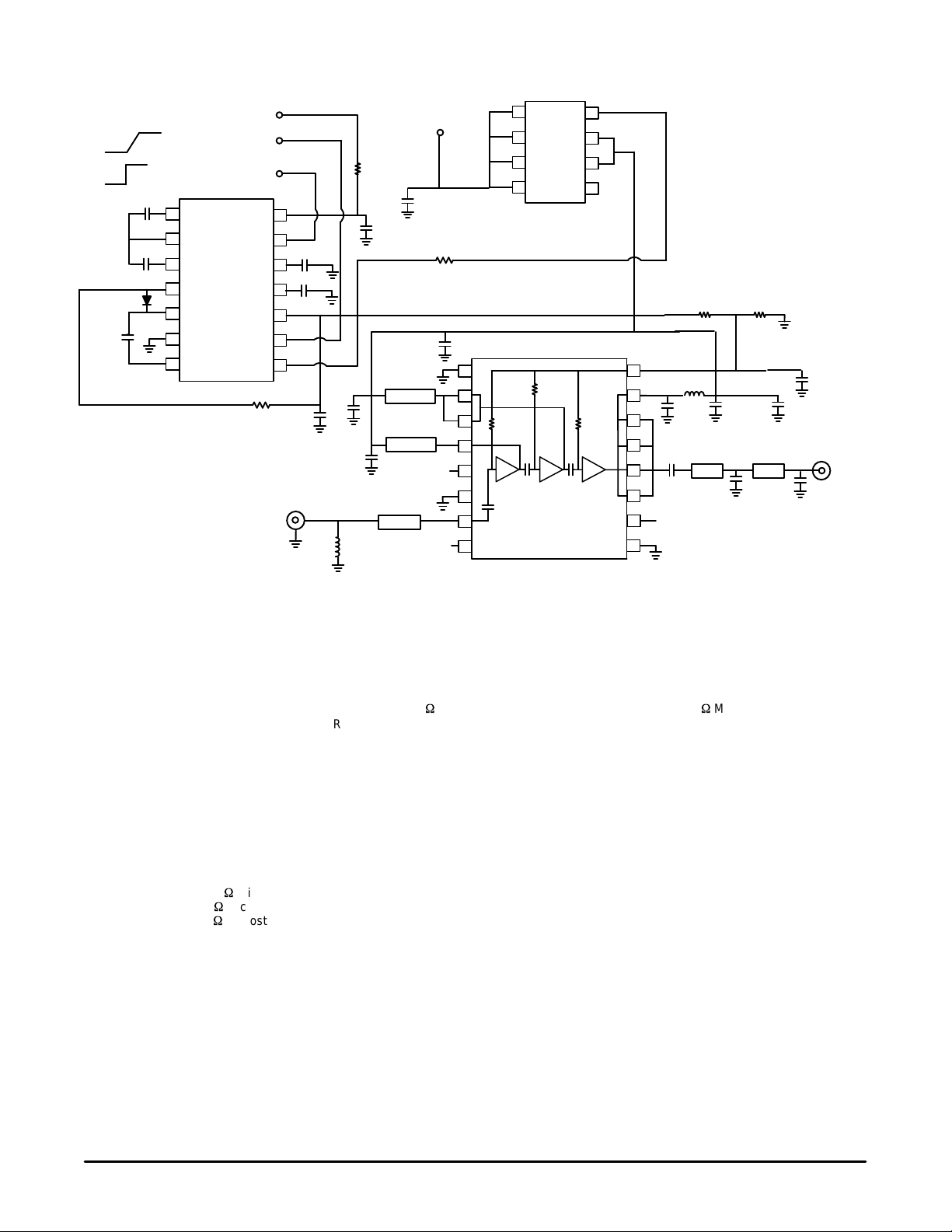
C1 6.8 nF
C2, C9, C10 22 pF, 0603 NPO/COG
C3, C11 47 nF
C20, C21 1 pF
CR1 MMBD701LT1
L1 18 nH, Coilcraft or 20 mm
C4 5.6 pF, AVX0603 ACCUF
C5 3.9 pF, AVX0603 ACCUF
C12 220 nF
C13, C16, C17, C19 1 µF
C14, C15 1 µF
C18 1 µF
L2 1.8 nH, Toko 2012
Q1 MMSF4N01HD
R1 2.7 K
R2 3 KΩ
R3 22 Ω
NOTE: For PCS1900 applications, the following
component values are changed
L2 = 1.5 nH Toko 2012
C4 = 6.8 pF, AVX0603 ACCUF
C5 = 2.7 pF, AVX0603 ACCUF
C20 = Not Used
T1 = 0.5 mm 50 W Microstrip Line
T2 = 5 mm 50 W Microstrip Line
T3 = 1 mm 40
Microstrip Line
Figure 2. DCS1800/PCS1900 Applications Circuit Configuration
50 Ω Microstrip Line
W
U1
R4 100 Ω
R5 470 Ω
T1 0.5 mm 30 Ω Microstrip Line
T2 5 mm 50 Ω Microstrip Line
T3 8 mm 50 Ω Microstrip Line
T4 1 mm 50 Ω Microstrip Line
T5 5.5 mm 50 W Microstrip Line
U1 MRFIC1817
U2 MC33169 (–4 V Version)
Board Material: Glass/Epoxy,
Thickness = 0.5 mm
ε
= 4.45,
r
MRFIC1817MOTOROLA RF DEVICE DATA
3
 Loading...