

Motorola MRFIC1814 Datasheet
SEMICONDUCTOR TECHNICAL DATA
The MRFIC Line
Designed primarily for use in wireless Personal Communication Systems
(PCS) applications such as Digital European Cordless Telephone (DECT),
Japan’s Personal Handy System (PHS), and the emerging North American
systems. The MRFIC1814 includes a low noise amplifier and downmixer in a
low-cost TSSOP–16 package. The integrated circuit requires minimal off-chip
matching while allowing for the maximum in flexibility and efficiency. The mixer
is optimized for low–side injection and offers reasonable intercept point as well
as high efficiency with 9 dB of conversion gain. Image filtering is implemented
off-chip to allow maximum flexibility. CMOS compatible ENABLE pins allow
standby operation where the current drain is less than 0.1 mA.
Together with the rest of the MRFIC180X series, this GaAs IC family offers
the complete transmit and receive functions, less LO and filters, needed for a
typical 1.8 GHz cordless telephone.
• Usable Frequency Range = 1.8 to 2.0 GHz
• 17 dB Typ Gain, 2.5 dB Typ Noise Figure LNA
• 8 dB Typ Gain, 10 dB Typ Noise Figure Mixer
• –5.5 dBm Typ Mixer Input Intercept Point
• Simple LO/IF Off-chip Matching for Maximum Flexibility
• Low Power Consumption = 39 mW (Typ)
• Single Bias Supply = 2.7 to 4.5 Volts
• Low LO Power Requirement = – 5 dBm (Typ)
• Low Cost Surface Mount Plastic Package
• Order MRFIC1814R2 for Tape and Reel.
R2 Suffix = 2,500 Units per 16 mm, 13 inch Reel.
• Device Marking = M1814
Order this document
by MRFIC1814/D
1.8 GHz LOW NOISE
AMPLIFIER AND
DOWNMIXER
CASE 948C–03
(TSSOP–16)
Motorola, Inc. 1997
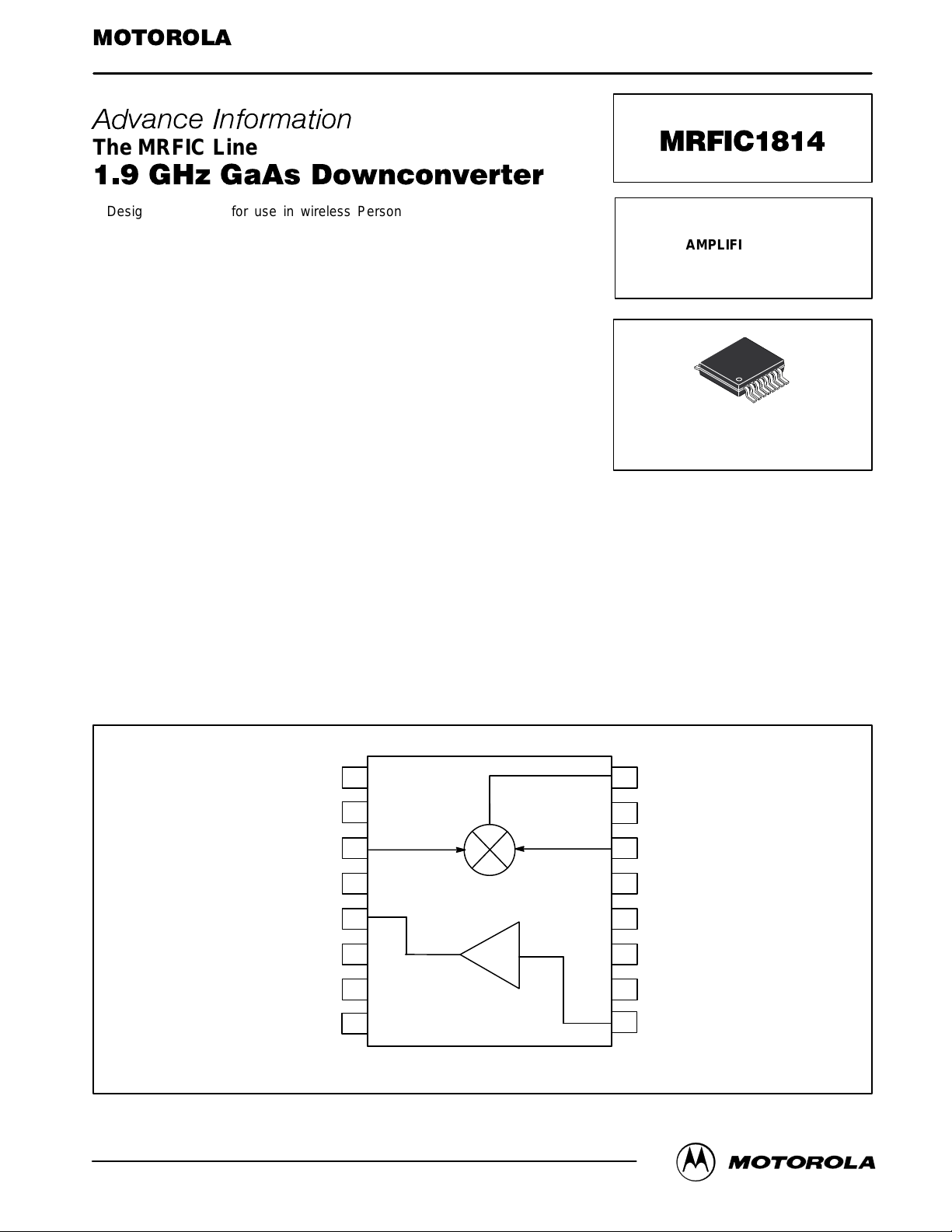
MIXER ENABLE
N/C
LO INPUT
V
DD2
LNA OUT
LNA CAP
N/C
LNA ENABLE
1
2
3
4
5
6
7
8
MIXER
LNA
16
15
14
13
12
11
10
9
Pin Connections and Functional Block Diagram
IF OUT/V
N/C
MIXER IN
GND
V
DD1
GND
GND
LNA IN
DD3
MRFIC1814MOTOROLA RF DEVICE DATA
1

MAXIMUM RATINGS (T
= 25°C unless otherwise noted)
A
Rating Symbol Limit Unit
Supply Voltage V
LNA Input Power LNA
LO Input Power P
Enable Voltage ENABLE 5.5 Vdc
Storage Temperature Range T
Operating Ambient Temperature T
DD
in
LO
stg
A
5.5 Vdc
10 dBm
10 dBm
– 65 to +150 °C
– 30 to +85 °C
RECOMMENDED OPERATING RANGES
Parameter
RF Input Frequency f
Mixer LO Frequency f
IF Output Frequency f
Supply Voltage V
Enable Voltage, ON MIXER, LNA ENABLE 2.7 to V
Enable Voltage, OFF MIXER, LNA ENABLE 0 to 0.2 Vdc
Symbol Value Unit
RF
LO
IF
DD
1.8 to 2.0 GHz
1.5 to 1.8 GHz
70 to 300 MHz
2.7 to 4.5 Vdc
DD
Vdc
ELECTRICAL CHARACTERISTICS (V
ENABLE = 3 V)
Characteristic
LNA Gain (LNA ENABLE = 3 V) 14 17 — dB
LNA Gain (LNA ENABLE = 0 V) — –19 — dB
LNA Noise Figure — 2.5 — dB
LNA Input 3rd Order Intercept — –7 — dBm
LNA Output 1 dB Gain Compression Point –6 –3 — dBm
Mixer Conversion Gain (into 50 Ω) 5 8 — dB
Mixer Noise Figure — 10 — dB
Mixer Input 3rd Order Intercept — –5 — dBm
Mixer Output 1 dB Gain Compression Point –8.5 –5.5 — dBm
Total Supply Current (ENABLE VOLTAGES = 3.0 V, LO off) — 10 17 mA
Total Supply Current (ENABLE VOLTAGES = 3.0 V, LO on) — 13 — mA
Standby Mode Current (ENABLE VOLTAGES = 0 V, LO off) — 0.05 0.25 mA
= 3 V, TA = 25°C, LO = 1.65 GHz @ – 5 dBm, RF = 1.9 GHz @ –30 dBm, MIXER & LNA
DD
Min Typ Max Unit
MRFIC1814
2
MOTOROLA RF DEVICE DATA
 Loading...