SEMICONDUCTOR TECHNICAL DATA
The MRFIC Line
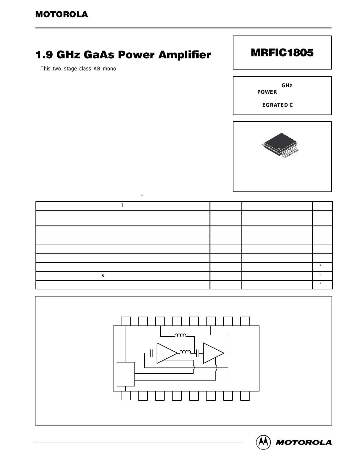
This two–stage class AB monolithic GaAs amplifier in a low–cost 16 lead
plastic package is designed for output or driver applications in 1.9 GHz PCS
handsets and basestations. The design is optimized for 3.0 Volt operation in
systems such as Japan’s PHS, Europe’s DECT and the emerging North
American PCS services. With modifications to the simple off–chip matching, the
device can be used in other applications from 1.5 to 2.5 GHz.
• High Output Capability = 27 dBm Typical P
21.5 dBm Typical with PHS Format
• High Gain = 21 dB Typical Small Signal, 20 dB at P
• Low Current Drain = 170 mA Typical with PHS Format
250 mA Typical with DECT Format
• Low–Cost, Low Profile Plastic TSSOP Package
• Order MRFIC1805R2 for Tape and Reel.
R2 Suffix = 2,500 Units per 16 mm, 13 inch Reel.
• Device Marking = M1805
sat
= 22 dBm
out
Order this document
by MRFIC1805/D
1.9 GHz
POWER AMPLIFIER
GaAs MONOLITHIC
INTEGRATED CIRCUIT
CASE 948C–03
(TSSOP–16)
ABSOLUTE MAXIMUM RATINGS (TA = 25_C unless otherwise noted)
Ratings Symbol Value Unit
Supply Voltage VDD, VD1,
Supply Voltage V
RF Input Power RF
Drain Current I
Thermal Resistance, Junction to Air R
Operating Junction Temperature T
Ambient Operating Temperature T
Storage Temperature T
PCNTRL
16
GND
15
GND
V
D1
RF OUT/
GND N/C
V
D2
V
D2
SS
in
DD
θJA
J
A
stg
RF OUT/
V
D2
6 Vdc
–4 Vdc
+10 dBm
500 mA
240 /W
+175
–30 to +85
–65 to +125
91011121314
_
C
_
C
_
C
REV 1
Motorola, Inc. 1997
MOTOROLA RF DEVICE DATA
GATE
BIAS
1
234
V
GND GND
SS
GND
GND GND N/C
RF IN
Pin Connections and Functional Block Diagram
8765
MRFIC1805
1

RECOMMENDED OPERATING CONDITIONS
Parameter Symbol Value Unit
Supply Voltage VDD, VD1,
Supply Voltage V
PA Control Voltage PCNTRL 0.0 to V
RF Input Power P
Operating Frequency Range f
V
D2
SS
in
OP
2.7 to 5 Vdc
–2.5 Vdc
–20 to +10 dBm
1500 to 2200 MHz
DD
Vdc
ELECTRICAL CHARACTERISTICS (V
IDQ = 125 mA, circuit configuration as shown in Figure 1)
Characteristic
Power Output, Saturation P
RF Output Power P
Adjacent Channel Power Ratio (384 Kbps p/4 DQPSK Signal,
600 kHz Offset, P
RF Output 1 dB Compression P
2nd Harmonic Output – – –40 – dBc
3rd Harmonic Output – – –40 – dBc
Supply Current I
Supply Current I
Supply Current I
Input Return Loss – – 13 – dB
Reverse Isolation – – 31 – dB
Output Third Intercept – – 34 – dBm
Turn On Time – – 1 –
= 21 dBm
out
PCNTRL
= VD2 = 3 Vdc, Vss = –2.5 Vdc, TA= 25_C, f = 1.9 GHz, Pin = +2 dBm, PCNTRL set for
D1
Symbol Min Typ Max Unit
23 25 – dBm
20 21.5 – dBm
– –58 –55 dBc
22 24 – dBm
– 170 210 mA
– 200 300 µA
– 220 300 µA
C5
RF OUT
C3
SAT
out
P
ACP
1dB
DD
SS
PCNTRL
V
DD
C4
T2
R1
C2
m
s
MRFIC1805
2
15
16
GATE
BIAS
1
C6
V
SS
R1 – 22
C1 – 1.2 pF
C2 – 2.2 pF
C3, C6 – 330 pF
34
2
W
C4, C5, – 22 pF
T1 – 100 W Line, 7 mm
T2 – 100 W Line, 20 mm
Board Material – 30 MIL FR4
Connectors – SMA Type
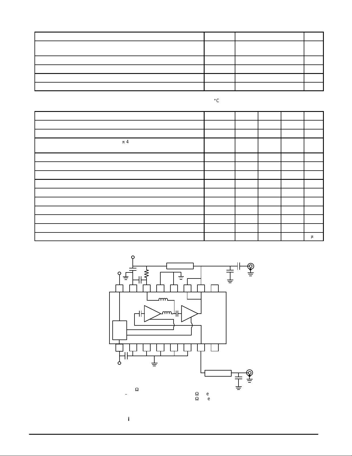
Figure 1. Applications Circuit Configuration
91011121314
8765
T1
C1
RF IN
MOTOROLA RF DEVICE DATA

TYPICAL CHARACTERISTICS
30
25
20
15
10
, OUTPUT POWER (dBm)
5
out
P
0
–5
–15 –5
–10
Pin, INPUT POWER (dBm)
2.5 V
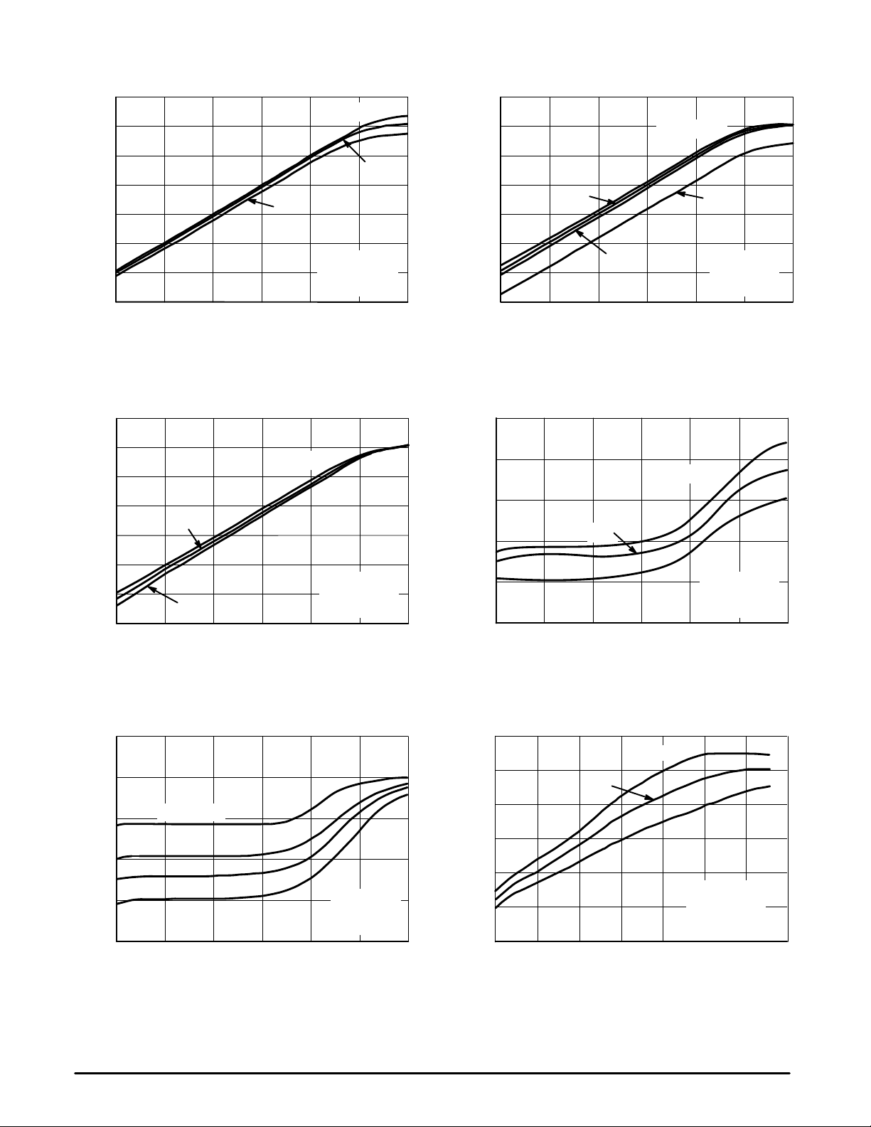
Figure 2. Output Power versus Input Power
30
25
20
15
10
, OUTPUT POWER (dBm)
5
out
P
0
–5
–20
85°C
–35°C
–10 10
Pin, INPUT POWER (dBm)
TA = 25°C
–5–15 5
VDD = 3.5 V
f = 1.9 GHz
I
DDQ
TA = 25
0
f = 1.9 GHz
I
DDQ
VDD = 3.0 V
0
3.0 V
= 125 mA
°
C
= 125 mA
30
25
20
15
10
, OUTPUT POWER (dBm)
5
out
P
0
–5
105
–20 0–20
–15
150 mA
125 mA
–10 –5
Pin, INPUT POWER (dBm)
I
DDQ
= 190 mA
100 mA
f = 1.9 GHz
VDD = 3.0 V
TA = 25
°
C
105
Figure 3. Output Power versus Input Power
300
250
VDD = 3.5 V
200
150
, SUPPLY CURRENT (mA)
DD
I
100
50
–15 –10–20
3.0 V
2.5 V
–5 0 10
Pin, INPUT POWER (dBm)
f = 1.9 GHz
I
= 125 mA
DDQ
TA = 25
°
C
5
Figure 4. Output Power versus Input Power
300
250
I
= 190 mA
200
150
, SUPPLY CURRENT (mA)
DD
I
100
50
–20
DDQ
150 mA
125 mA
100 mA
–10 0
Pin, INPUT POWER (dBm)
–5
Figure 6. Supply Current versus Input Power
MOTOROLA RF DEVICE DATA
f = 1.9 GHz
VDD = 3.0 V
TA = 25
°
C
510
Figure 5. Supply Current versus Input Power
300
VDD = 3.5 V
250
200
150
100
, SUPPLY CURRENT (mA)
DD
I
50
0
0.5–15
3.0 V
1.0
1.5
P
, CONTROL VOLTAGE (V)
CNTRL
2.5 V
f = 1.9 GHz
I
= 125 mA
DDQ
Pin = +10 dBm
TA = 25
°
2.0 2.5 3.0
Figure 7. Supply Current versus Control Voltage
MRFIC1805
C
3.50.0
3
 Loading...