

Freescale Semiconductor, Inc.
Order this document by MRFIC0930/D
nc...
, I
or
查询"MRFIC0930"供应商
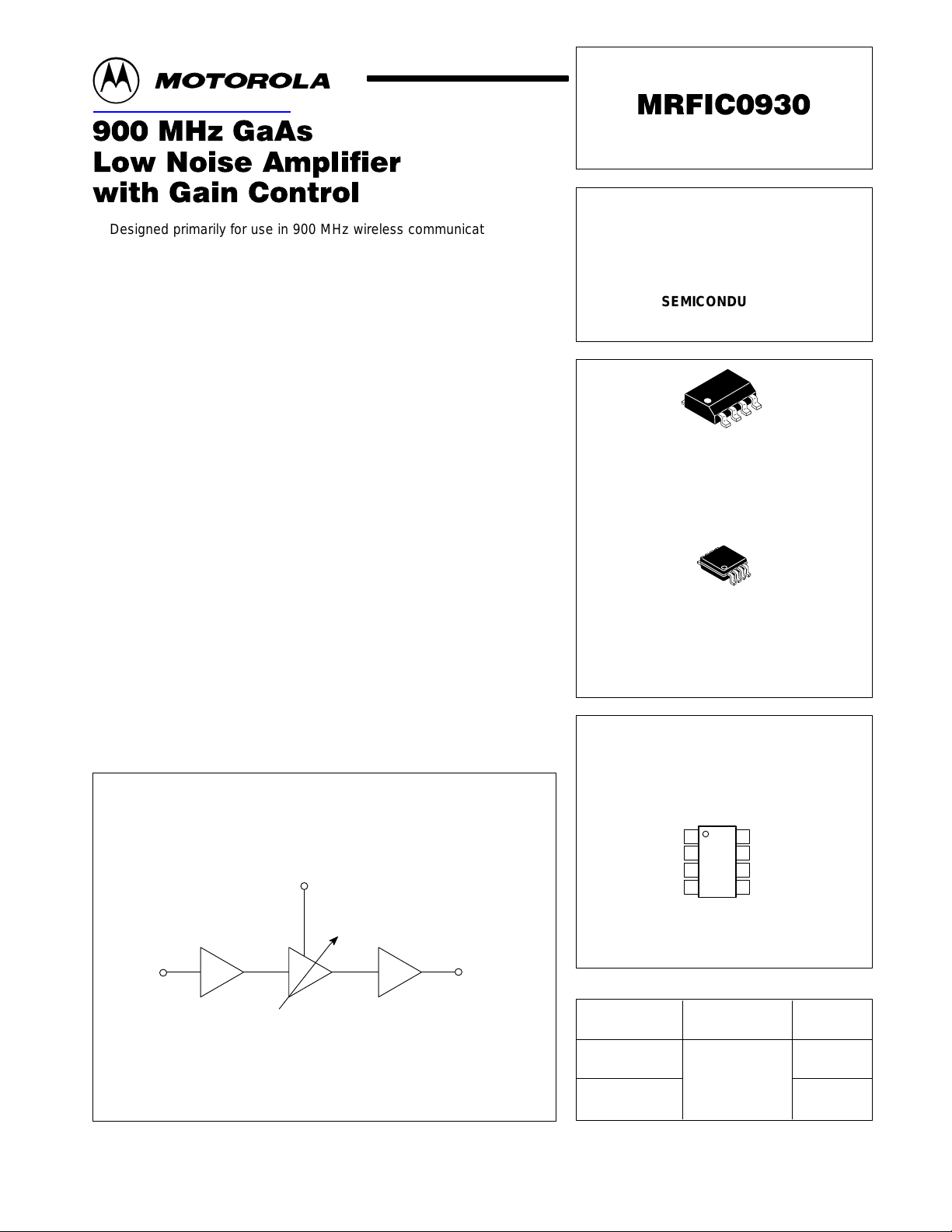
Designed primarily for use in 900 MHz wireless communication systems
such as GSM, AMPS, and Industrial, Scientific, and Medical (ISM) band
applications. The MRFIC0930 is a two–stage low noise amplifier with an
integrated step attenuator and is packaged in a low–cost SO–8 package.
The MRFIC0930DM is packaged in the smaller Micro–8 package. The
attenuator is controlled by a V
transmit mode to save current by using the Rx Enable Pin. The amplifier can
be matched to optimize gain or noise figure with simple off–chip input
matching.
• Usable Frequency Range = 800 to 1000 MHz
• 19 dB Typ Gain
• Gain Attenuation = 18 dB (Typ)
• 1.7 dB Typ Noise Figure
• Simple Off–chip Matching for Maximum Gain/Noise Figure Flexibility
• High Reverse Isolation = 41 dB (Typ)
• Low Power Consumption = 24 mW (Typ)
• Single Bias Supply = 2.7 to 4.5 V
• Low Standby Current = 20 µA (Typ)
• Low Cost Surface Mount Plastic Package
Pin. The LNA can be turned off during
gain
900 MHz GaAs
LOW NOISE AMPLIFIER
WITH GAIN CONTROL
SEMICONDUCTOR
TECHNICAL DATA
8
1
(Scale 2:1)
PLASTIC PACKAGE
CASE 751
(SO–8, Tape & Reel Only)
8
1
(Scale 2:1)
emiconduct
Simplified Block Diagram
eescale S
Fr
DEVICE ON LIFETIME BUY
RF In RF Out/V
This device contains 12 active transistors.
MOTOROLA RF/IF DEVICE DATA
V
gain
D2
For More Information On This Product,
Go to: www.freescale.com
DM SUFFIX
PLASTIC PACKAGE
CASE 846A
(Micro–8, Tape & Reel Only)
PIN CONNECTIONS
1
RF In
2
Gnd
3
V
D1
Rx Enable
ORDERING INFORMATION
Device
MRFIC0930R2
MRFIC0930DMR2
Motorola, Inc. 1999 Rev 2
4
(Top View)
TA = –30 to 70°C
*2,500 Units per 16 mm, 13 inch reel.
**2,500 Units per 12 mm, 13 inch reel.
8
Gnd
7
V
6
Gnd
5
RF Out/V
Operating
Temp Range
gain
D2
Package
SO–8*
Tape & Reel
Micro–8**
Tape & Reel
1
LAST ORDER 28SEP01 LAST SHIP 28SEP02
Freescale Semiconductor, Inc.
MRFIC0930
nc...
, I
or
MAXIMUM RATINGS (T
查询"MRFIC0930"供应商
Supply Voltage VD1, V
RF Input Power P
Gain Control Voltage V
Enable Voltage RX Enable 5.5 Vdc
Storage Temperature Range T
Operating Ambient Temperature T
NOTES: 1. Meets Human Body Model (HBM) ≤750 V and Machine Model (MM) ≤100 V.
2.ESD data available upon request.
RECOMMENDED OPERATING RANGES
RF Frequency f
Supply Voltage VD1, V
V
, High Gain V
gain
V
, Low Gain V
gain
Rx Enable Voltage, On Rx Enable 2.7 – VD1, V
Rx Enable Voltage, Of f Rx Enable 0 – 0.2 Vdc
NOTE: To bias, apply VD1 and VD2 before Rx Enable.
= 25°C, unless otherwise noted)
A
Rating
Parameter Symbol Min Typ Max Unit
Symbol Value Unit
D2
RF
gain
stg
A
5.5 Vdc
3 dBm
5.5 Vdc
–65 to 150 °C
–30 to 70 °C
RF
D2
gain
gain
800 – 1000 MHz
2.7 – 4.5 Vdc
– 3.0 – Vdc
– 0 – Vdc
D2
Vdc
emiconduct
eescale S
Fr
ELECTRICAL CHARACTERISTICS (V
unless otherwise noted. Tested in Circuit Shown in Figure 1.)
Characteristic
RF Gain S
MRFIC0930 17 19 21
MRFIC0930DM 17.5 19 21.5
RF Gain (V
SSB Noise Figure [Note] NF – 1.7 3.0 dB
SSB Noise Figure (V
RF Input 3rd Order Intercept Point [Note] IIP3 –12 –9.0 – dBm
RF Input 3rd Order Intercept Point (V
Input 1.0 dB Gain Compression [Note] P
Input 1.0 dB Gain Compression (V
Reverse Isolation (S12) S
Input Return Loss S
DEVICE ON LIFETIME BUY
Input Return Loss (V
Output Return Loss S
Output Return Loss (V
Supply Current Rx Mode I
Supply Current Standby Mode (Rx Enable = 0 V) I
NOTE: Guaranteed by design.
= 0 V) S
gain
= 0 V) [Note] NF – 10.4 – dB
gain
gain
= 0 V) S
gain
= 0 V) S
gain
D1, VD2
= 0 V) [Note] IIP3 –7.0 –5.7 – dBm
gain
= 0 V) [Note] P
= 2.8 V, TA = 25°C, RF = 940 MHz, Rx Enable = 2.8 V, V Gain = 2.8 V, RF In = –30 dBm,
Symbol Min Typ Max Unit
21
21
1dB
1dB
12
11
11
22
22
D
D
– 0.8 4.0 dB
–21.5 –20.8 – dBm
–16 –11 – dBm
– 41 – dB
– 15 – dB
– 15 – dB
– 15 – dB
– 12 – dB
– 8.5 12 mA
– 20 200
dB
m
A
LAST ORDER 28SEP01 LAST SHIP 28SEP02
2
For More Information On This Product,
Go to: www.freescale.com
MOTOROLA RF/IF DEVICE DATA
Freescale Semiconductor, Inc.
MRFIC0930
nc...
, I
or
查询"MRFIC0930"供应商
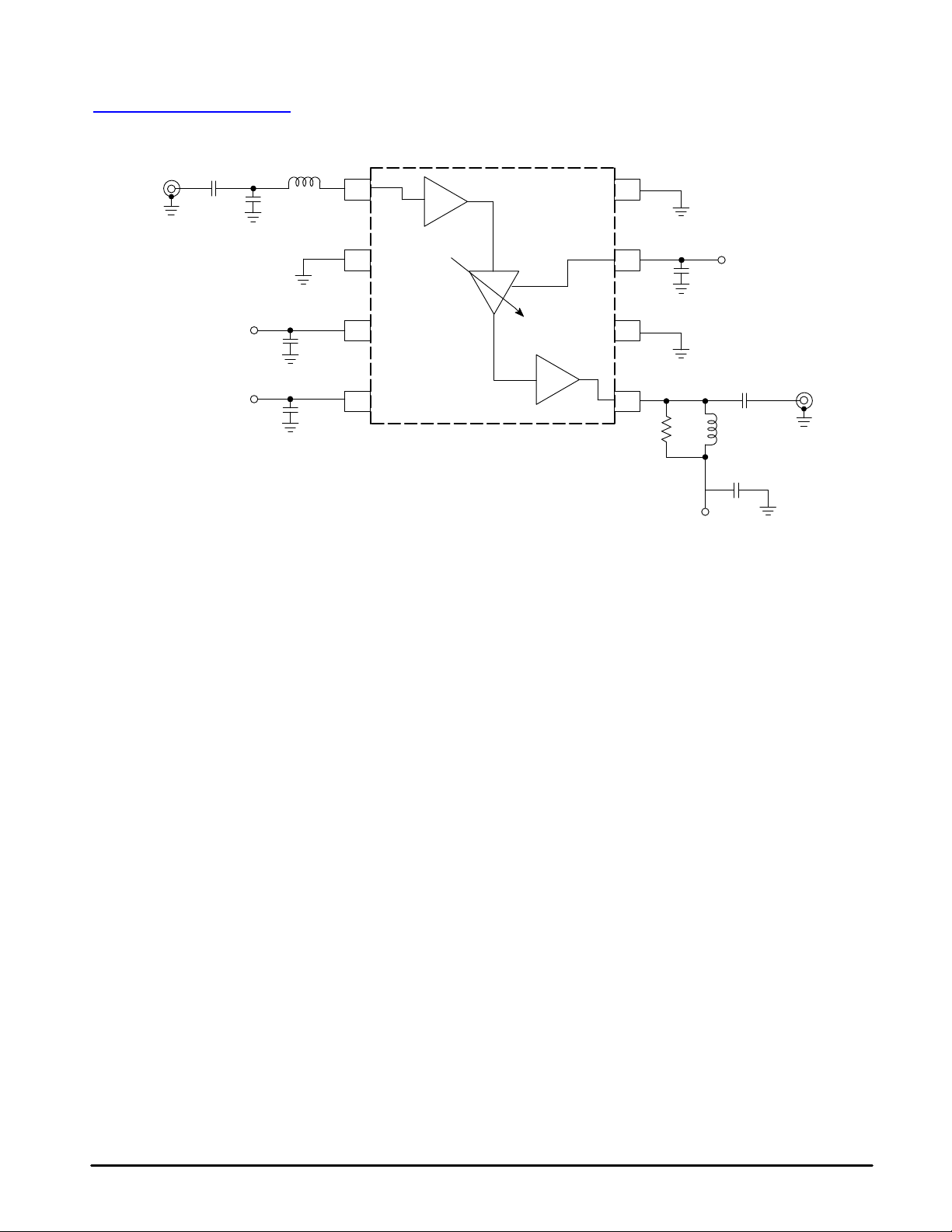
RF In
C3
C1
V
D1
Rx Enable
For MRFIC0930:
C1 = 2.2 pF
C2 = 2.1 pF
C3, C4, C5, C6, C7 = 1,000 pF
L1 = 18 nH
L2 = 10 nH
Ω
R1 = 220
L1
C5
C6
Figure 1. 900 MHz Test Circuit
1
2
3
4
For MRFIC0930DM:
C1 = 1.3 pF
C2 = 2.1 pF
C3, C4, C5, C6, C7 = 1000 pF
L1 = 22 nH
L2 = 8.2 nH
Ω
R1 = 180
8
7
6
5
R1 L2
C7
V Gain
C2
C4
V
D2
RF Out
emiconduct
eescale S
Fr
DEVICE ON LIFETIME BUY
MOTOROLA RF/IF DEVICE DATA
For More Information On This Product,
Go to: www.freescale.com
LAST ORDER 28SEP01 LAST SHIP 28SEP02
3

0
0
0
查询"MRFIC0930"供应商
Freescale Semiconductor, Inc.
MRFIC0930
TYPICAL CHARACTERISTICS
(For SO–8 Packaged MRFIC0930)
nc...
, I
or
emiconduct
Figure 2. Reverse Isolation versus Frequency
–40
–41
–42
–43
–44
REVERSE ISOLATION (dB)
–45
–46
800 820 840 860 880 900 920 940 960 980 1000
22
20
18
GAIN (dB)
16
14
800 820 840 860 880 900 920 940 960 980 1000
TA = –25°C
70°C
25°C
VD = 2.8 V
V
gain
f, FREQUENCY (MHz)
Figure 4. Gain versus Frequency
TA = –25°C
70°C
25°C
f, FREQUENCY (MHz)
VD = 2.8 V
V
gain
Pin = –30 dBm
= 2.8 V
= 0 V
Figure 3. Reverse Isolation versus Frequency
–39
–40
–41
–42
–43
ISOLATION (dB)
–44
–45
–46
800 820 840 860 880 900 920 940 960 980 100
Figure 5. Gain Attenuation versus Frequency
18.8
18.6
18.4
18.2
18
GAIN ATTENUA TION (dB)
17.8
17.6
800 820 840 860 880 900 920 940 960 980 100
TA = –25°C
70°C
f, FREQUENCY (MHz)
TA = –25°C
25°C
f, FREQUENCY (MHz)
25°C
VD = 2.8 V
V
gain
70°C
VD = 2.8 V
V
= 0 V
gain
Pin = –30 dBm
= 2.8 V
eescale S
Figure 6. Gain versus Frequency
Fr
DEVICE ON LIFETIME BUY
22
20
18
16
GAIN (dB)
14
12
10
800
4
820 840 860 880 900 920 940 960 980 1000
VD = 4.5 V
3.0 V
f, FREQUENCY (MHz)
2.8 V
V
= V
gain
D
TA = 25
°
C
Pin = –30 dBm
For More Information On This Product,
Go to: www.freescale.com
19.424
19.2
18.8
18.6
18.4
18.2
GAIN ATTENUA TION (dB)
17.8
17.6
19
18
Figure 7. Gain Attenuation versus Frequency
VD = 4.5 V
3.0 V
2.8 V
800 820 840 860 880 900 920 940 960 980 100
f, FREQUENCY (MHz)
MOTOROLA RF/IF DEVICE DATA
V
= V
gain
D
TA = 25
°
C
Pin = –30 dBm
LAST ORDER 28SEP01 LAST SHIP 28SEP02

0
查询"MRFIC0930"供应商
Freescale Semiconductor, Inc.
MRFIC0930
TYPICAL CHARACTERISTICS
(For SO–8 Packaged MRFIC0930)
nc...
, I
or
emiconduct
Figure 8. Input Power versus Output Power
4.0
VD = 4.5 V
0
–4.0
, OUTPUT POWER (dBm)
–8.0
out
P
–12
–30 –28 –26 –24 –22 –20 –18 –16 –14 –12 –10
Figure 10. Input Power versus Output Power
4.0
2.0
0
–2.0
–4.0
–6.0
–8.0
, OUTPUT POWER (dBm)
–10
out
P
–12
–14
–30 –28 –26 –24 –22 –20 –18 –16 –14 –12 –10
3.0 V
2.8 V
Pin, INPUT POWER (dBm)
TA = –25°C
25°C
Pin, INPUT POWER (dBm)
f = 940 MHz
TA = 25
V
= V
gain
70°C
f = 940 MHz
VD = 2.8 V
V
= 2.8 V
gain
Figure 9. Input Power versus Output Power
–4.0
–8.0
–12
–16
–20
, OUTPUT POWER (dBm)
–24
out
°
C
D
P
–28
–32
–30 –28 –26 –24 –22 –20 –18 –16 –14 –12 –10
Figure 11. Input Power versus Output Power
–10
–15
–20
3.0 V
Pin, INPUT POWER (dBm)
VD = 4.5 V
2.8 V
TA = –25°C
f = 940 MHz
°
C
TA = 25
V
= 0 V
gain
70°C
–25
, OUTPUT POWER (dBm)
–30
out
P
–35
–30 –28 –26 –24 –22 –20 –18 –16 –14 –12 –10
Pin, INPUT POWER (dBm)
25°C
f = 940 MHz
VD = 2.8 V
V
= 0 V
gain
eescale S
Figure 12. Noise Figure versus Frequency Figure 13. Noise Figure versus Frequency
Fr
3.0
DEVICE ON LIFETIME BUY
2.5
2.0
1.5
NF , NOISE FIGURE (dBm)
1.0
0.5
800 820 840 860 880 900 920 940 960 980 1000
MOTOROLA RF/IF DEVICE DATA
70°C
25°C
TA = –25°C
f, FREQUENCY (MHz)
For More Information On This Product,
VD = 2.8 V
V
= 2.8 V
gain
Go to: www.freescale.com
16
15
14
13
12
11
10
NF , NOISE FIGURE (dBm)
9.0
8.0
VD = 2.8 V
V
= 0 V
gain
70°C
25°C
TA = –25°C
800 820 840 860 880 900 920 940 960 980 100
f, FREQUENCY (MHz)
5
LAST ORDER 28SEP01 LAST SHIP 28SEP02

0
0
查询"MRFIC0930"供应商
Freescale Semiconductor, Inc.
MRFIC0930
TYPICAL CHARACTERISTICS
(For Micro–8 Packaged MRFIC0930DM)
nc...
, I
or
emiconduct
Figure 14. Reverse Isolation versus Frequency
–46
25°C
–48
–50
REVERSE ISOLATION (dB)
–52
800 850 950 1000
22
20
18
GAIN (dB)
16
14
800 840 880 920 960 1000
Figure 16. Gain versus Frequency
TA = 70°C
–25°C
VD = 2.8 V
V
900
f, FREQUENCY (MHz)
TA = –25°C
70°C
f, FREQUENCY (MHz)
= 2.8 V
gain
VD = 2.8 V
V
= 2.8 V
gain
Pin = –30 dBm
25°C
Figure 15. Reverse Isolation versus Frequency
–45
TA = 70°C
25°C
–47
–49
REVERSE ISOLATION (dB)
–51
800 850 900 950 100
f, FREQUENCY (MHz)
Figure 17. Gain Attenuation versus Frequency
20
TA = –25°C
19.5
19
GAIN ATTENUA TION (dB)
18.5
800 820 840 860 880 900 920 940 960 980 1000
25°C
f, FREQUENCY (MHz)
–25°C
VD = 2.8 V
V
= 0 V
gain
70°C
VD = 2.8 V
V
= 0 V
gain
Pin = –30 dBm
eescale S
Figure 18. Gain versus Frequency
Fr
DEVICE ON LIFETIME BUY
20
GAIN (dB)
15
10
800
6
850 900 950 1000
f, FREQUENCY (MHz)
4.5 V
3.0 V
2.8 V
V
= V
gain
D
TA = 25
°
C
Pin = –30 dBm
For More Information On This Product,
Go to: www.freescale.com
20.525
19.5
18.5
GAIN ATTENUA TION (dB)
17.5
20
19
18
17
Figure 19. Gain Attenuation versus Frequency
VD = 4.5 V
3.0 V
2.8 V
V
= 0 V
gain
°
C
TA = 25
Pin = –30 dBm
800 820 840 860 880 900 920 940 960 980 100
f, FREQUENCY (MHz)
MOTOROLA RF/IF DEVICE DATA
LAST ORDER 28SEP01 LAST SHIP 28SEP02

0
查询"MRFIC0930"供应商
Freescale Semiconductor, Inc.
MRFIC0930
TYPICAL CHARACTERISTICS
(For Micro–8 Packaged MRFIC0930DM)
nc...
, I
or
Figure 20. Input Power versus Output Power
8.0
4.5 V
4.0
3.0 V
0
–4.0
, OUTPUT POWER (dBm)
out
–8.0
P
–12
–30 –26 –22 –18 –14 –10
Pin, INPUT POWER (dBm)
Figure 22. Input Power versus Output Power
4.0
TA = –25°C
0
f = 940 MHz
TA = 25
V
= V
gain
°
C
70°C
2.8 V
D
Figure 21. Input Power versus Output Power
–5.0
–10
3.0 V
–15
–20
, OUTPUT POWER (dBm)
out
–25
P
–30
–30 –26 –22 –18 –14 –10
Pin, INPUT POWER (dBm)
Figure 23. Input Power versus Output Power
–10
–15
–25°C
4.5 V
2.8 V
f = 940 MHz
TA = 25
V
= 0 V
gain
°
C
70°C
emiconduct
–4.0
, OUTPUT POWER (dBm)
–8.0
out
P
–12
–30 –28 –26 –24 –22 –20 –18 –16 –14 –12 –10
Pin, INPUT POWER (dBm)
25°C
f = 940 MHz
VD = 2.8 V
V
= 2.8 V
gain
–20
, OUTPUT POWER (dBm)
–25
out
P
–35
eescale S
Figure 24. Noise Figure versus Frequency Figure 25. Noise Figure versus Frequency
Fr
4.0
DEVICE ON LIFETIME BUY
3.0
TA = 70°C
2.0
1.0
NF , NOISE FIGURE (dBm)
0
800 820 840 860 880 900 920 940 960 980 1000
f, FREQUENCY (MHz)
25°C
–25°C
VD = 2.8 V
V
= 2.8 V
gain
16
15
10
NF , NOISE FIGURE (dBm)
8.0
25°C
f = 940 MHz
VD = 2.8 V
V
= 0 V
gain
–30 –28 –26 –24 –22 –20 –18 –16 –14 –12 –10
Pin, INPUT POWER (dBm)
VD = 2.8 V
V
= 0 V
gain
TA = 70°C
–25°C
800 820 840 860 880 900 920 940 960 980 100
f, FREQUENCY (MHz)
25°C
LAST ORDER 28SEP01 LAST SHIP 28SEP02
MOTOROLA RF/IF DEVICE DATA
For More Information On This Product,
Go to: www.freescale.com
7

Freescale Semiconductor, Inc.
MRFIC0930
nc...
, I
or
emiconduct
查询"MRFIC0930"供应商
A
E
B
C
A1
PIN 1 ID
SEATING
PLANE
–T–
0.038 (0.0015)
D
58
1
e
K
G
4
B
–A–
H
0.25MB
H
A
SEATING
PLANE
0.10
SS
A0.25MCB
–B–
8 PL
D
0.08 (0.003) A
C
M
J
OUTLINE DIMENSIONS
PLASTIC PACKAGE
CASE 751–06
(SO–8)
ISSUE T
C
M
h
X 45
_
q
L
PLASTIC PACKAGE
CASE 846A–02
(Micro–8)
ISSUE D
S
B
T
S
L
NOTES:
1. DIMENSIONING AND TOLERANCING PER ASME
Y14.5M, 1994.
2. DIMENSIONS ARE IN MILLIMETER.
3. DIMENSION D AND E DO NOT INCLUDE MOLD
PROTRUSION.
4. MAXIMUM MOLD PROTRUSION 0.15 PER SIDE.
5. DIMENSION B DOES NOT INCLUDE DAMBAR
PROTRUSION. ALLOWABLE DAMBAR
PROTRUSION SHALL BE 0.127 TOTAL IN EXCESS
OF THE B DIMENSION AT MAXIMUM MATERIAL
CONDITION.
MILLIMETERS
DIM MIN MAX
A 1.35 1.75
A1 0.10 0.25
B 0.35 0.49
C 0.19 0.25
D 4.80 5.00
E
3.80 4.00
1.27 BSCe
H 5.80 6.20
h
0.25 0.50
L 0.40 1.25
0 7
q
NOTES:
1. DIMENSIONING AND TOLERANCING PER ANSI
Y14.5M, 1982.
2. CONTROLLING DIMENSION: MILLIMETER.
3. DIMENSION A DOES NOT INCLUDE MOLD FLASH,
PROTRUSIONS OR GATE BURRS. MOLD FLASH,
PROTRUSIONS OR GATE BURRS SHALL NOT
EXCEED 0.15 (0.006) PER SIDE.
4. DIMENSION B DOES NOT INCLUDE INTERLEAD
FLASH OR PROTRUSION. INTERLEAD FLASH OR
PROTRUSION SHALL NOT EXCEED 0.25 (0.010)
PER SIDE.
DIM MIN MAX MIN MAX
A 2.90 3.10 0.114 0.122
B 2.90 3.10 0.114 0.122
C ––– 1.10 ––– 0.043
D 0.25 0.40 0.010 0.016
G 0.65 BSC 0.026 BSC
H 0.05 0.15 0.002 0.006
J 0.13 0.23 0.005 0.009
K 4.75 5.05 0.187 0.199
L 0.40 0.70 0.016 0.028
__
INCHESMILLIMETERS
eescale S
Fr
Motorola reserves the right to make changes without further notice to any products herein. Motorola makes no warranty , representation or guarantee regarding
the suitability of its products for any particular purpose, nor does Motorola assume any liability arising out of the application or use of any product or circuit, and
specifically disclaims any and all liability, including without limitation consequential or incidental damages. “T ypical” parameters which may be provided in Motorola
data sheets and/or specifications can and do vary in different applications and actual performance may vary over time. All operating parameters, including “Typicals”
DEVICE ON LIFETIME BUY
must be validated for each customer application by customer’s technical experts. Motorola does not convey any license under its patent rights nor the rights of
others. Motorola products are not designed, intended, or authorized for use as components in systems intended for surgical implant into the body, or other
applications intended to support or sustain life, or for any other application in which the failure of the Motorola product could create a situation where personal injury
or death may occur. Should Buyer purchase or use Motorola products for any such unintended or unauthorized application, Buyer shall indemnify and hold Motorola
and its officers, employees, subsidiaries, affiliates, and distributors harmless against all claims, costs, damages, and expenses, and reasonable attorney fees
arising out of, directly or indirectly, any claim of personal injury or death associated with such unintended or unauthorized use, even if such claim alleges that
Motorola was negligent regarding the design or manufacture of the part. Motorola and are registered trademarks of Motorola, Inc. Motorola, Inc. is an Equal
Opportunity/Affirmative Action Employer.
How to reach us:
USA/EUROPE/Locations Not Listed: Motorola Literature Distribution; JAPAN: Motorola Japan Ltd.; SPD, Strategic Planning Office, 141,
P.O. Box 5405, Denver, Colorado 80217. 1–303–675–2140 or 1–800–441–2447 4–32–1 Nishi–Gotanda, Shinagawa–ku, Tokyo, Japan. 81–3–5487–8488
Customer Focus Center: 1–800–521–6274
Mfax: RMFAX0@email.sps.mot.com – TOUCHTONE 1–602–244–6609 ASIA/PACIFIC: Motorola Semiconductors H.K. Ltd.; Silicon Harbour Centre,
Motorola Fax Back System – US & Canada ONLY 1–800–774–1848 2, Dai King Street, Tai Po Industrial Estate, Tai Po, N.T., Hong Kong.
HOME PAGE: http://motorola.com/sps/
8
– http://sps.motorola.com/mfax/ 852–26629298
◊
For More Information On This Product,
Go to: www.freescale.com
Mfax is a trademark of Motorola, Inc.
MOTOROLA RF/IF DEVICE DATA
MRFIC0930/D
LAST ORDER 28SEP01 LAST SHIP 28SEP02
 Loading...